EP4379822A1 - Conductive layer structure and light-emitting device - Google Patents
Conductive layer structure and light-emitting device Download PDFInfo
- Publication number
- EP4379822A1 EP4379822A1 EP22855695.7A EP22855695A EP4379822A1 EP 4379822 A1 EP4379822 A1 EP 4379822A1 EP 22855695 A EP22855695 A EP 22855695A EP 4379822 A1 EP4379822 A1 EP 4379822A1
- Authority
- EP
- European Patent Office
- Prior art keywords
- conductive layer
- layer
- adhesion
- light emitting
- adhesion layer
- Prior art date
- Legal status (The legal status is an assumption and is not a legal conclusion. Google has not performed a legal analysis and makes no representation as to the accuracy of the status listed.)
- Pending
Links
- 239000012212 insulator Substances 0.000 claims description 22
- 239000000463 material Substances 0.000 claims description 21
- 229910052802 copper Inorganic materials 0.000 claims description 10
- 238000007772 electroless plating Methods 0.000 claims description 10
- 238000009713 electroplating Methods 0.000 claims description 10
- 229910052759 nickel Inorganic materials 0.000 claims description 10
- 229910052763 palladium Inorganic materials 0.000 claims description 10
- 229910052709 silver Inorganic materials 0.000 claims description 10
- 229910052782 aluminium Inorganic materials 0.000 claims description 8
- 229910052737 gold Inorganic materials 0.000 claims description 7
- 229910052750 molybdenum Inorganic materials 0.000 claims description 4
- 229910052697 platinum Inorganic materials 0.000 claims description 4
- 229910052703 rhodium Inorganic materials 0.000 claims description 4
- 229910052721 tungsten Inorganic materials 0.000 claims description 4
- 229910008599 TiW Inorganic materials 0.000 claims description 3
- 229910052745 lead Inorganic materials 0.000 claims description 3
- 229910052749 magnesium Inorganic materials 0.000 claims description 3
- 229910052710 silicon Inorganic materials 0.000 claims description 3
- 229910052718 tin Inorganic materials 0.000 claims description 3
- 229910052719 titanium Inorganic materials 0.000 claims description 3
- 229910052725 zinc Inorganic materials 0.000 claims description 3
- 238000010030 laminating Methods 0.000 claims description 2
- 239000010410 layer Substances 0.000 description 825
- 238000000034 method Methods 0.000 description 59
- 230000008569 process Effects 0.000 description 34
- 238000004519 manufacturing process Methods 0.000 description 21
- 239000000758 substrate Substances 0.000 description 13
- 239000004065 semiconductor Substances 0.000 description 12
- 230000006866 deterioration Effects 0.000 description 9
- QVGXLLKOCUKJST-UHFFFAOYSA-N atomic oxygen Chemical compound [O] QVGXLLKOCUKJST-UHFFFAOYSA-N 0.000 description 8
- 229910052760 oxygen Inorganic materials 0.000 description 8
- 239000001301 oxygen Substances 0.000 description 8
- 238000007747 plating Methods 0.000 description 8
- 230000000694 effects Effects 0.000 description 7
- 238000005516 engineering process Methods 0.000 description 7
- 230000003245 working effect Effects 0.000 description 7
- 238000000206 photolithography Methods 0.000 description 5
- 238000005530 etching Methods 0.000 description 4
- 238000004544 sputter deposition Methods 0.000 description 4
- 229910001218 Gallium arsenide Inorganic materials 0.000 description 3
- 238000001704 evaporation Methods 0.000 description 3
- 230000008020 evaporation Effects 0.000 description 3
- 238000004020 luminiscence type Methods 0.000 description 3
- 229910000980 Aluminium gallium arsenide Inorganic materials 0.000 description 2
- 230000004888 barrier function Effects 0.000 description 2
- 239000007769 metal material Substances 0.000 description 2
- 239000000203 mixture Substances 0.000 description 2
- 238000012986 modification Methods 0.000 description 2
- 230000004048 modification Effects 0.000 description 2
- VYPSYNLAJGMNEJ-UHFFFAOYSA-N Silicium dioxide Chemical compound O=[Si]=O VYPSYNLAJGMNEJ-UHFFFAOYSA-N 0.000 description 1
- 239000012790 adhesive layer Substances 0.000 description 1
- 239000000956 alloy Substances 0.000 description 1
- 230000004075 alteration Effects 0.000 description 1
- 229910052785 arsenic Inorganic materials 0.000 description 1
- 230000015572 biosynthetic process Effects 0.000 description 1
- 230000008878 coupling Effects 0.000 description 1
- 238000010168 coupling process Methods 0.000 description 1
- 238000005859 coupling reaction Methods 0.000 description 1
- 229910052733 gallium Inorganic materials 0.000 description 1
- 229910021478 group 5 element Inorganic materials 0.000 description 1
- 238000003384 imaging method Methods 0.000 description 1
- 239000012535 impurity Substances 0.000 description 1
- 229910052738 indium Inorganic materials 0.000 description 1
- 239000004973 liquid crystal related substance Substances 0.000 description 1
- 229910052751 metal Inorganic materials 0.000 description 1
- 239000002184 metal Substances 0.000 description 1
- 229910052757 nitrogen Inorganic materials 0.000 description 1
- 238000000059 patterning Methods 0.000 description 1
- 229910052698 phosphorus Inorganic materials 0.000 description 1
- 239000002096 quantum dot Substances 0.000 description 1
- 229910052814 silicon oxide Inorganic materials 0.000 description 1
- 239000002356 single layer Substances 0.000 description 1
Images




Classifications
-
- H—ELECTRICITY
- H01—ELECTRIC ELEMENTS
- H01S—DEVICES USING THE PROCESS OF LIGHT AMPLIFICATION BY STIMULATED EMISSION OF RADIATION [LASER] TO AMPLIFY OR GENERATE LIGHT; DEVICES USING STIMULATED EMISSION OF ELECTROMAGNETIC RADIATION IN WAVE RANGES OTHER THAN OPTICAL
- H01S5/00—Semiconductor lasers
- H01S5/04—Processes or apparatus for excitation, e.g. pumping, e.g. by electron beams
- H01S5/042—Electrical excitation ; Circuits therefor
- H01S5/0425—Electrodes, e.g. characterised by the structure
-
- H—ELECTRICITY
- H01—ELECTRIC ELEMENTS
- H01S—DEVICES USING THE PROCESS OF LIGHT AMPLIFICATION BY STIMULATED EMISSION OF RADIATION [LASER] TO AMPLIFY OR GENERATE LIGHT; DEVICES USING STIMULATED EMISSION OF ELECTROMAGNETIC RADIATION IN WAVE RANGES OTHER THAN OPTICAL
- H01S5/00—Semiconductor lasers
- H01S5/04—Processes or apparatus for excitation, e.g. pumping, e.g. by electron beams
- H01S5/042—Electrical excitation ; Circuits therefor
- H01S5/0425—Electrodes, e.g. characterised by the structure
- H01S5/04256—Electrodes, e.g. characterised by the structure characterised by the configuration
-
- H—ELECTRICITY
- H10—SEMICONDUCTOR DEVICES; ELECTRIC SOLID-STATE DEVICES NOT OTHERWISE PROVIDED FOR
- H10H—INORGANIC LIGHT-EMITTING SEMICONDUCTOR DEVICES HAVING POTENTIAL BARRIERS
- H10H20/00—Individual inorganic light-emitting semiconductor devices having potential barriers, e.g. light-emitting diodes [LED]
- H10H20/80—Constructional details
- H10H20/83—Electrodes
- H10H20/831—Electrodes characterised by their shape
- H10H20/8316—Multi-layer electrodes comprising at least one discontinuous layer
-
- H—ELECTRICITY
- H10—SEMICONDUCTOR DEVICES; ELECTRIC SOLID-STATE DEVICES NOT OTHERWISE PROVIDED FOR
- H10H—INORGANIC LIGHT-EMITTING SEMICONDUCTOR DEVICES HAVING POTENTIAL BARRIERS
- H10H20/00—Individual inorganic light-emitting semiconductor devices having potential barriers, e.g. light-emitting diodes [LED]
- H10H20/80—Constructional details
- H10H20/83—Electrodes
- H10H20/831—Electrodes characterised by their shape
-
- H—ELECTRICITY
- H10—SEMICONDUCTOR DEVICES; ELECTRIC SOLID-STATE DEVICES NOT OTHERWISE PROVIDED FOR
- H10H—INORGANIC LIGHT-EMITTING SEMICONDUCTOR DEVICES HAVING POTENTIAL BARRIERS
- H10H20/00—Individual inorganic light-emitting semiconductor devices having potential barriers, e.g. light-emitting diodes [LED]
- H10H20/80—Constructional details
- H10H20/83—Electrodes
- H10H20/832—Electrodes characterised by their material
-
- H—ELECTRICITY
- H01—ELECTRIC ELEMENTS
- H01S—DEVICES USING THE PROCESS OF LIGHT AMPLIFICATION BY STIMULATED EMISSION OF RADIATION [LASER] TO AMPLIFY OR GENERATE LIGHT; DEVICES USING STIMULATED EMISSION OF ELECTROMAGNETIC RADIATION IN WAVE RANGES OTHER THAN OPTICAL
- H01S5/00—Semiconductor lasers
- H01S5/04—Processes or apparatus for excitation, e.g. pumping, e.g. by electron beams
- H01S5/042—Electrical excitation ; Circuits therefor
- H01S5/0425—Electrodes, e.g. characterised by the structure
- H01S5/04252—Electrodes, e.g. characterised by the structure characterised by the material
-
- H—ELECTRICITY
- H01—ELECTRIC ELEMENTS
- H01S—DEVICES USING THE PROCESS OF LIGHT AMPLIFICATION BY STIMULATED EMISSION OF RADIATION [LASER] TO AMPLIFY OR GENERATE LIGHT; DEVICES USING STIMULATED EMISSION OF ELECTROMAGNETIC RADIATION IN WAVE RANGES OTHER THAN OPTICAL
- H01S5/00—Semiconductor lasers
- H01S5/10—Construction or shape of the optical resonator, e.g. extended or external cavity, coupled cavities, bent-guide, varying width, thickness or composition of the active region
- H01S5/18—Surface-emitting [SE] lasers, e.g. having both horizontal and vertical cavities
- H01S5/183—Surface-emitting [SE] lasers, e.g. having both horizontal and vertical cavities having only vertical cavities, e.g. vertical cavity surface-emitting lasers [VCSEL]
-
- H—ELECTRICITY
- H10—SEMICONDUCTOR DEVICES; ELECTRIC SOLID-STATE DEVICES NOT OTHERWISE PROVIDED FOR
- H10H—INORGANIC LIGHT-EMITTING SEMICONDUCTOR DEVICES HAVING POTENTIAL BARRIERS
- H10H20/00—Individual inorganic light-emitting semiconductor devices having potential barriers, e.g. light-emitting diodes [LED]
- H10H20/80—Constructional details
- H10H20/83—Electrodes
- H10H20/831—Electrodes characterised by their shape
- H10H20/8312—Electrodes characterised by their shape extending at least partially through the bodies
Definitions
- the present disclosure relates to a conductive layer structure, and to a light emitting device.
- PTL 1 discloses a semiconductor device including a capacitance element.
- the capacitance element includes a lower electrode, a dielectric film on the lower electrode, and an upper electrode on the dielectric film.
- An insulating film is formed on the upper electrode with an adhesion layer interposed, and a contact hole is formed to penetrate through the adhesion layer and the insulating film in a thickness direction.
- the insulating film for example, a silicon oxide film is used, and the adhesion layer includes Ti, for example.
- metal wiring is coupled via the contact hole.
- Ti included in the adhesion layer deteriorates and becomes for example, oxidized.
- a Ti oxide is a high-resistance material, increasing resistance of a current path.
- an increase in resistance is likely to cause an increase in drive voltage or a luminescence failure.
- a conductive layer structure includes a first conductive layer, a third conductive layer that is electrically coupled to the first conductive layer with an adhesion layer interposed, and a second conductive layer that is electrically coupled to the third conductive layer.
- the adhesion layer has conductivity and has a higher adhesiveness to each of the first conductive layer and the third conductive layer than adhesiveness between the first conductive layer and the third conductive layer.
- the second conductive layer is less likely to deteriorate than the adhesion layer, covers an end and an upper surface of the adhesion layer while covering a portion of the first conductive layer.
- a conductive layer structure includes a first conductive layer, a fourth conductive layer that is formed on the first conductive layer with an insulator interposed, and a second conductive layer having one end coupled to the first conductive layer with an adhesion layer interposed, a middle portion laminated on an insulator, and another end coupled to the fourth conductive layer with the adhesion layer interposed in between.
- the adhesion layer has conductivity, and has a higher adhesiveness to each of the first, the second, and the fourth conductive layers than adhesiveness between the first conductive layer and the second conductive layer or adhesiveness between the fourth conductive layer and the second conductive layer.
- the second conductive layer is less likely to deteriorate than the adhesion layer, and covers an end surface and an upper surface of the adhesion layer while covering a portion of the first conductive layer and a portion of the fourth conductive layer.
- a first embodiment is a first example in which the present technique is applied to a conductive layer structure and a light emitting device including the conductive layer structure.
- the light emitting device is a vertical cavity surface emitting laser (VCSEL: Vertical Cavity Surface Emitting Laser) as an example.
- VCSEL Vertical Cavity Surface Emitting Laser
- a method of manufacturing the conductive layer structure will also be described in particular.
- a second embodiment describes a second example in which a configuration of the conductive layer structure is changed in the conductive layer structure and the light emitting device according to the first embodiment.
- a third embodiment describes a third example in which a configuration of the conductive layer structure is changed in the conductive layer structure and the light emitting device according to the first embodiment.
- a fourth embodiment is a fourth example in which the present technique is applied to a conductive layer structure and a light emitting device including the conductive layer structure.
- the light emitting device is a light emitting diode (LED: Light Emitting Diode) as an example.
- a conductive layer structure 3 and a light emitting device 1 according to a first embodiment of the present disclosure will be described with reference to FIG. 1 , FIGs. 2A to 2C , FIGs. 3A to 3C , and FIGs. 4A to 4C .
- an arrow X direction which is illustrated in figures as appropriate, indicates one planar direction of the conductive layer structure 3 and the light emitting device 1 that are disposed on a planar surface for a descriptive purpose.
- An arrow Y direction indicates another planar direction orthogonal to the arrow X direction.
- an arrow Z direction indicates an upper direction orthogonal to the arrow X direction and the arrow Y direction.
- the arrow X, Y, and Z directions just correspond to X, Y, and Z axes of a three-dimensional coordinate system, respectively.
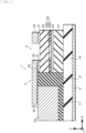
- FIG. 1 illustrates a longitudinal sectional configuration of an example of the conductive layer structure 3 and the light emitting device 1 according to the first embodiment of the present disclosure.
- the light emitting device 1 includes a light emitting element 2. Furthermore, the light emitting device 1 includes the conductive layer structure 3.
- the light emitting element 2 is laminated on a substrate 10 as a base in a region a lateral surface of which is surrounded by an insulator 11.
- the light emitting element 2 is a VCSEL as a surface emitting laser.
- the light emitting element 2 includes a first reflection layer 21, an emission layer 22, a current constriction layer 23, and a second reflection layer 24, each as a major component.
- a plurality of light emitting elements 2 is arranged in each of the arrow X direction and the arrow Y direction with the insulator 11 interposed.
- the conductive layer structure 3 includes a first conductive layer 31 and a second conductive layer 32 that is electrically coupled to the first conductive layer 31 with an adhesion layer 35 interposed.
- the conductive layer structure 3 further includes a fourth conductive layer 34 that is formed with the insulator 11 interposed in the first conductive layer 31.
- the second conductive layer 32 has one end coupled to the first conductive layer 31 and has another end coupled to the fourth conductive layer 34 with the adhesion layer 35 interposed.
- a middle portion of the second conductive layer 32 is laminated on the insulator 11 with the adhesion layer 35 interposed.
- the substrate 10 is used as an epitaxial growth substrate.
- n-type GaAs is used for example.
- the "first conductivity type" is described as "n-type.”
- S is used as an n-type impurity.
- a buffer layer may be laminated on the substrate 10.
- the buffer layer is laminated, it is possible to configure a terrace and step structure having high smoothness.
- a contact layer 4 is provided on an opposite (back surface) side of the substrate 10 to a side on which the light emitting element is laminated.
- the contact layer 4 supplies an electric current to the light emitting elements 2.
- the first reflection layer 21 is laminated directly on the substrate 10, or laminated on the substrate 10 with a buffer layer interposed, an illustration of which is omitted.
- the first reflection layer 21 is a semiconductor DBR (Distributed Bragg Reflector).
- the first reflection layer 21 has a configuration in which a plurality of semiconductor layers having two or more types with different refractive indices is alternately laminated.
- a plurality of semiconductor layers each including n-type AlGaAs or n-type GaAs is alternately laminated.
- the first reflection layer 21 may include a dielectric DBR, for example.
- the light emitting layer 22 is laminated on the first reflection layer 21.
- the light emitting layer 22 has a configuration in which a plurality of layers including a barrier layer and a quantum well layer is alternately laminated.
- barrier layer for example, non-doped AlGaInAs is used.
- the quantum well layer includes at least one element selected from Al, Ga, and In among group III elements, and at least one element selected from As, P, and N among group V elements.
- the quantum well layer includes non-doped AlGaInAs as a main component.
- the light emitting layer 22 may be configured as a strain-compensation quantum well.
- a current constriction layer 23 is laminated on the light emitting layer 22.
- the current constriction layer 23 includes a current passage region 23A that is formed in a middle portion and a current constriction region 23B that is formed in a periphery of the current passage region 23A.
- the current passage region 23A has a circular shape when viewed from the arrow Z direction (hereinafter simply referred to as "in planar view").
- the current constriction region 23B includes an oxide or an ion-implanted region.
- a second reflection layer 24 is laminated on the current constriction layer 23.
- the second reflection layer 24 is a semiconductor DBR.
- the second reflection layer 24 has a configuration in which a plurality of semiconductor layers having two or more types with different refractive indices is alternately laminated.
- the second reflection layer 24 has a configuration in which a plurality of semiconductor layers each including p-type AlGaAs or p-type GaAs as the second conductivity type is alternately laminated.
- the second reflection layer 24 may include a dielectric DBR, for example.
- the first conductive layer 31 is laminated on the second reflection layer 24 of the light emitting element 2 and formed along a periphery of the second reflection layer 24.
- the first conductive layer 31 is formed in a shape of a ring with a missing portion.
- the first conductive layer 31 is formed as an electrode of the light emitting element 2 or a contact layer.
- the first conductive layer 31 includes a multilayer film in which Au, Pt, and Ti are each sequentially laminated.
- Au is formed to have a thickness of 50 nm or more and 500 nm or less.
- Pt is formed to have a thickness of 10 nm or more and 100 nm or less.
- Ti is formed to have a thickness of 10 nm or more and 100 nm or less.
- the first conductive layer 31 it is possible to include at least one material selected from Au, Al, Cu, Ag, Rh, W, Mo, Ni, Pd, ITO, ITiO, ZnO, and AuGe.
- Au, Al, Cu, Ag, Rh, W, Mo, Ni, and Pd are each a metal material.
- ITO, ITiO, and ZnO are each a transparent metal material.
- AuGe is an alloy material. It is possible to use these materials as a monolayer film or as a multilayer film.
- the fourth conductive layer 34 is formed on the substrate 10 in an outer periphery of the light emitting element 2 with the insulator 11 interposed.
- the fourth conductive layer 34 is configured as wiring that supplies an electric current to the light emitting element 2.
- the fourth conductive layer 34 includes Au, for example.
- Au is formed to have a thickness of 0.5 ⁇ m or more and 5 ⁇ m or less.
- the fourth conductive layer 34 may include a material similar to the material given as an example in the first conductive layer 31.
- the adhesion layer 35 is formed from the first conductive layer 31 to the fourth conductive layer 34.
- the adhesion layer 35 has one end laminated on the first conductive layer 31, and has another end laminated on the fourth conductive layer 34.
- a middle portion of the adhesion layer 35 is formed on the insulator 11.
- a position of an end surface of the adhesion layer 35 excluding a connection point between the first conductive layer 31 and the fourth conductive layer 34, is set inside a position of an end surface of the first conductive layer 31.
- the position of the end surface of the adhesion layer 35 is set inside a position of an end surface of the fourth conductive layer 34.
- the adhesion layer 35 has a higher adhesiveness (or adhesion) to each of the first conductive layer 31, the second conductive layer 32, and the fourth conductive layer 34 than adhesiveness between the first conductive layer and the second conductive layer 32 and adhesiveness between the fourth conductive layer 34 and the second conductive layer 32.
- Ti is used, for example.
- Ti is formed to have a thickness of 10 nm or more and 100 nm or less.
- adhesion layer 35 it is possible to include, other than Ti as described above, at least one material selected from Ni, Al, Pd, Mg, Si, Cu, Ag, and TiW.
- the second conductive layer 32 is configured as an electrode on each of the first conductive layer 31 and the fourth conductive layer 34. Furthermore, the second conductive layer 32 is configured as bridge wiring that electrically couples two layers from the first conductive layer 31 to the fourth conductive layer 34.
- the second conductive layer 32 is formed in a state of covering an end surface and an upper surface of the adhesion layer 35. Compared to the adhesion layer 35, the second conductive layer 32 includes a material that is less likely to deteriorate even when exposed to a high temperature and high humidity environment. For example, the second conductive layer 32 includes a material that is less likely to be oxidated or nitrided than the adhesion layer 35.
- the second conductive layer 32 also covers the first conductive layer 31 and is also electrically coupled to the first conductive layer 31. Then, another portion of the second conductive layer 32 covers the fourth conductive layer 34 likewise and is also electrically coupled to the fourth conductive layer 34.
- the second conductive layer 32 is configured to cover the adhesion layer 35 while covering a portion from the adhesion layer 35 to each of the first conductive layer 31 and the fourth conductive layer 34. As a result, an entry route to an interface between the adhesion layer 35 and the first conductive layer 31 and an entry route to an interface between the adhesion layer 35 and the fourth conductive layer 34 are each blocked by the second conductive layer 32.
- the second conductive layer 32 includes Au.
- Au is formed using an electrolytic plating method or an electroless plating method.
- the second conductive layer 32 is formed to have a greater thickness than the adhesion layer 35, for example, to a thickness of 0.5 ⁇ m or more and 3.0 ⁇ m or less.
- the second conductive layer 32 it is possible to include, other than Au as described above, at least one material selected from Cu, Ni, Co, Sn, Pt, Ag, Pb, Zn, and Pd. It is possible to include all of these materials by a plating method.
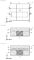
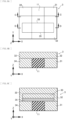
- FIGs. 2A , 3A , and 4A each illustrate a planar surface in each process, which describes the method of manufacturing the conductive layer structure 3.
- FIG. 2B illustrates a process cross section of the conductive layer structure 3 taken along section line A-A illustrated in FIG. 2A
- FIG. 2C illustrates a process cross section of the conductive layer structure 3 taken along section line B-B illustrated in FIG. 2A
- FIG. 3B illustrates a process cross section of the conductive layer structure 3 taken along section line A-A illustrated in FIG. 3A
- FIG. 3C illustrates a process cross section of the conductive layer structure 3 take along section line B-B illustrated in FIG. 3A .
- FIG. 3C illustrates a process cross section of the conductive layer structure 3 take along section line B-B illustrated in FIG. 3A .
- FIG. 4B illustrates a process cross section of the conductive layer structure 3 taken along section line A-A illustrated in FIG. 4A
- FIG. 4C illustrates a process cross section of the conductive layer structure 3 taken along section line B-B illustrated in FIG. 4A .
- each of the first conductive layer 31 and the fourth conductive layer 34 is formed as illustrated in FIGs. 2A to 2C .
- the first conductive layer 31 is formed on the second reflection layer 24 of the light emitting element 2.
- the first conductive layer 31 is formed by evaporation, sputtering, plating, or the like.
- the fourth conductive layer 34 is formed at a position separated from the light emitting element 2 with the insulator 11 interposed with respect to the first conductive layer 31.
- the fourth conductive layer 34 is formed by evaporation, sputtering, plating, or the like.
- the adhesion layer 35 is formed on a portion from the first conductive layer 31 to the fourth conductive layer 34.
- the adhesion layer 35 is formed using sputtering or the like.
- the second conductive layer 32 is formed in a state of covering the adhesion layer 35 including the end surface and upper surface of the adhesion layer 35.
- a portion of the second conductive layer 32 is also formed on the first conductive layer 31, and the second conductive layer 32 is electrically coupled to the first conductive layer 31.
- another portion of the second conductive layer 32 is also formed on the fourth conductive layer 34, and the second conductive layer 32 is electrically coupled to the fourth conductive layer 34.
- the second conductive layer 32 is formed as bridge wiring that couples the first conductive layer 31 and the fourth conductive layer 34.
- the second conductive layer 32 is formed using an electrolytic plating method or an electroless plating method. This forms the second conductive layer 32 selectively on an exposed surface of each of the first conductive layer 31, the fourth conductive layer 34, and the adhesion layer 35. Accordingly, in forming the second conductive layer 32, it is not necessary to use photolithography and etching technologies.
- the conductive layer structure 3 includes the first conductive layer 31 and the second conductive layer 32.
- the second conductive layer 32 is electrically coupled to the first conductive layer 31 with the adhesion layer 35 interposed.
- the adhesion layer 35 has conductivity and has a higher adhesiveness to each of the first conductive layer 31 and the second conductive layer 32 than adhesiveness between the first conductive layer 31 and the second conductive layer 32.
- the second conductive layer 32 is less likely to deteriorate than the adhesion layer 35, and couples a portion of the adhesion layer 35 to the first conductive layer 31 in a state of covering the adhesion layer 35 including an end surface thereof.
- the adhesion layer 35 is covered by the second conductive layer 32 in a state where the adhesiveness between the first conductive layer 31 and the second conductive layer 32 is increased by the adhesion layer 35. In other words, even when exposed to a high temperature and high humidity environment, a route for oxygen or the like to enter the adhesion layer 35 is blocked. This makes it possible to effectively suppress or prevent an increase in resistance of a current path due to a deterioration of the adhesion layer 35.
- a portion of the second conductive layer 32 is directly and electrically coupled to the first conductive layer 31, thus making it possible to further reduce the resistance of the current path from the first conductive layer 31 to the second conductive layer 32.
- the second conductive layer 32 has a greater thickness than the adhesion layer 35. This increases an overall thickness of the conductive layer structure 3, making it possible to further reduce the resistance of the current path.
- the second conductive layer 32 is a plating layer formed by an electrolytic plating method or an electroless plating method, as illustrated in FIG. 1 , FIGs. 2A to 2C , and FIGs. 3A to 3C .
- the second conductive layer 32 covers the adhesion layer 35 including the end and upper surfaces thereof, and is further formed on a surface of the first conductive layer 31 exposed from the adhesion layer 35, to be formed from the adhesion layer 35 to the first conductive layer 31.
- a portion of the second conductive layer 32 is directly and electrically coupled to the first conductive layer 31, thus making it possible to further reduce the resistance of the current path from the first conductive layer 31 to the second conductive layer 32.
- the conductive layer structure 3 includes the first conductive layer 31, the fourth conductive layer 34, and the second conductive layer 32.
- the fourth conductive layer 34 is formed with the insulator 11 interposed in the first conductive layer 31.
- the second conductive layer 32 has one end coupled to the first conductive layer 31 with the adhesion layer 35 interposed, has a middle portion formed at the insulator 11, and has another end coupled to the fourth conductive layer 34 with the adhesion layer 35 interposed.
- the adhesion layer 35 has conductivity and has a higher adhesiveness to each of the first conductive layer 31, the second conductive layer 32, and the fourth conductive layer 34 than adhesiveness between the first conductive layer 31 and the second conductive layer 32 or adhesiveness between the fourth conductive layer 34 and the second conductive layer 32. Then, the second conductive layer 32 is less likely to deteriorate than the adhesion layer 35, and couples a portion of the adhesion layer 35 to the first conductive layer 31 while coupling another portion of the adhesion layer 35 to the fourth conductive layer 34 in a state of covering the adhesion layer 35 including an end surface and an upper surface thereof.
- the adhesion layer 35 is covered by the second conductive layer 32 in a state where the adhesiveness between the first conductive layer 31 and the second conductive layer 32 and the adhesiveness between the fourth conductive layer 34 and the second conductive layer 32 are increased by the adhesion layer 35.
- a route for oxygen or the like to enter the adhesion layer 35 is blocked. This makes it possible to effectively suppress or prevent an increase in resistance of a current path due to a deterioration of the adhesion layer 35.
- a portion of the second conductive layer 32 is directly and electrically coupled to each of the first conductive layer 31 and the fourth conductive layer 34, thus making it possible to further reduce the resistance of the current path from the first conductive layer 31 to the fourth conductive layer 34 through the second conductive layer 32.
- the light emitting device 1 includes the light emitting element 2 and the conductive layer structure 3.
- the conductive layer structure 3 is coupled to the light emitting element 2 and supplies an electric current to the light emitting element 2.
- the conductive layer structure 3 includes the first conductive layer 31 and the second conductive layer 32.
- the second conductive layer 32 is electrically coupled to the first conductive layer 31 with the adhesion layer 35 interposed.
- the adhesion layer 35 has conductivity and has a higher adhesiveness to each of the first conductive layer 31 and the second conductive layer 32 than adhesiveness between the first conductive layer 31 and the second conductive layer 32.
- the second conductive layer 32 is less likely to deteriorate than the adhesion layer 35, and couples a portion of the adhesion layer 35 to the first conductive layer 31 in a state of covering the adhesion layer 35 including an end surface and an upper surface thereof.
- the adhesion layer 35 is covered by the second conductive layer 32 in a state where the adhesiveness between the first conductive layer 31 and the second conductive layer 32 is increased by the adhesion layer 35. In other words, even when exposed to a high temperature and high humidity environment, a route for oxygen or the like to enter the adhesion layer 35 is blocked. This makes it possible to effectively suppress or prevent an increase in resistance of a current path due to a deterioration of the adhesion layer 35.
- a portion of the second conductive layer 32 is directly and electrically coupled to the first conductive layer 31, thus making it possible to further reduce the resistance of the current path from the first conductive layer 31 to the second conductive layer 32.
- the current path in the conductive layer structure 3 has a small resistance, thus making it possible to effectively suppress or prevent an increase in drive voltage and a luminescence failure.
- a conductive layer structure 3 and a light emitting device 1 according to a second embodiment of the present disclosure will be described with reference to FIG. 5 . It is to be noted that in the second and subsequent embodiments, the same reference numerals will be given to the same components or substantially the same components as those of the conductive layer structure 3 and the light emitting device 1 according to the first embodiment, and the overlapping description thereof will be omitted.
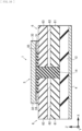
- FIG. 5 illustrates a longitudinal sectional configuration of an example of the conductive layer structure 3 and the light emitting device 1 according to the second embodiment.
- the light emitting device 1 according to the second embodiment includes the conductive layer structure 3.
- the conductive layer structure 3 includes a first conductive layer 31 that is formed on a second reflection layer 24 of the light emitting element 2, and a second conductive layer 32 that is electrically coupled to the first conductive layer 31 with an adhesion layer 35 interposed in the first conductive later 31.
- a fourth conductive layer 34 is formed around an outer periphery of the light emitting element 2.
- the conductive layer structure 3 electrically couples the second conductive layer 32 and the fourth conductive layer 34 by wire 5.
- the wire 5 is formed using an ultrasonic bonding method in combination with ultrasonic vibration.
- Au wire is used for the wire 5.
- the wire 5 is not limited to Au wire.
- the wire 5 it is possible to use Al wire, Cu wire, or the like.
- Components other than the above are the same as those of the conductive layer structure 3 and the light emitting device 1 according to the first embodiment.
- a conductive layer structure 3 and a light emitting device 1 according to a third embodiment of the present disclosure will be described with reference to FIG. 6 , FIGs. 7A to 7C , FIGs. 8A to 8C , and FIGs. 9A to 9C .
- FIG. 6 illustrates a longitudinal sectional configuration of an example of the conductive layer structure 3 and the light emitting device 1 according to the third embodiment.
- the light emitting device 1 according to the third embodiment includes the conductive layer structure 3.
- the conductive layer structure 3 includes a first conductive layer 31 that is formed on a second reflective layer 24 of the light emitting element 2, a third conductive layer 33 that is electrically coupled to the first conductive layer 31 with an adhesion layer 35 interposed, and a second conductive layer 32 that is electrically coupled to the third conductive layer 33.
- a fourth conductive layer 34 is formed around an outer periphery of the light emitting element 2.
- the fourth conductive layer 34 includes the third conductive layer 33 that is electrically coupled to the fourth conductive layer 34 with the adhesion layer 35 interposed, and the second conductive layer 32 that is electrically coupled to the third conductive layer 33.
- the adhesion layer 35, the third conductive layer 33, and the second conductive layer 32 are formed from the first conductive layer 31 to the fourth conductive layer 34, to be included in bridge wiring.
- the third conductive layer 33 is formed in the same planar shape as a planar shape of the adhesion layer 35.
- the adhesion layer 35 is patterned using the same mask formed by photolithography technology to pattern the third conductive layer 33.
- the third conductive layer 33 includes Au.
- the third conductive layer 33 is formed to have a thickness of 10 nm or more and 100 nm or less.
- the third conductive layer 33 other than Au, it is possible to use a material given as an example in the first conductive layer 31 described earlier.
- the second conductive layer 32 is formed on a surface of the third conductive layer 33, and is also formed on the surface of each of the adhesion layer 35, the first conductive layer 31, and the fourth conductive layer 34 that are exposed from the third conductive layer 33.
- Components other than the above are the same as those of the conductive layer structure 3 and the light emitting device 1 according to the first embodiment.
- FIGs. 7A to 9A illustrate a planar surface in each process, which describes the method of manufacturing the conductive layer structure 3.
- FIG. 7B illustrates a process cross section of the conductive layer structure 3 taken along section line C-C illustrated in FIG. 7A
- FIG. 7C illustrates a process cross section of the conductive layer structure 3 taken along section line D-D illustrated in FIG. 7A
- FIG. 8B illustrates a process cross section of the conductive layer structure 3 taken along section line C-C illustrated in FIG. 8A
- FIG. 8C illustrates a process cross section of the conductive layer structure 3 taken along section line D-D illustrated in FIG. 8A
- FIG. 9B illustrates a process cross section of the conductive layer structure 3 taken along section line C-C illustrated in FIG. 9A
- FIG. 9C illustrates a process cross section of the conductive layer structure 3 taken along section line D-D illustrated in FIG. 9A .
- each of the first conductive layer 31 and the fourth conductive layer 34 is formed as illustrated in FIGs 7A to 7C .
- the first conductive layer 31 is formed on the second reflective layer 24 of the light emitting element 2.
- the fourth conductive layer 34 is formed at a position separated from the light emitting element 2 with the insulator 11 interposed with respect to the first conductive layer 31.
- the adhesion layer 35 and the third conductive layer 33 are formed on a portion from the first conductive layer 31 to the fourth conductive layer 34.
- the third conductive layer 33 is formed to be laminated on the adhesion layer 35.
- the third conductive layer 33 is formed using evaporation, sputtering, or the like.
- the third conductive layer 33 and the adhesion layer 35 are patterned by etching technology, using the same mask formed by photolithography technology.
- the second conductive layer 32 is formed in a state of covering the adhesion layer 35 and the third conductive layer 33, including an end surface of the adhesion layer 35.
- a portion of the second conductive layer 32 is also formed on the first conductive layer 31, and the second conductive layer 32 is electrically coupled to the first conductive layer 31.
- another portion of the second conductive layer 32 is also formed on the fourth conductive layer 34, and the second conductive layer 32 is electrically coupled to the fourth conductive layer 34.
- the second conductive layer 32 is formed as bridge wiring that couples the first conductive layer 31 and the fourth conductive layer 34.
- the second conductive layer 32 is formed by an electrolytic plating method or an electroless plating method. This forms the second conductive layer 32 selectively on an exposed surface of each of the first conductive layer 31, the fourth conductive layer 34, and the third conductive layer 33. Accordingly, in forming the second conductive layer 32, it is not necessary to use photolithography and etching technologies.
- the conductive layer structure 3 and the light emitting device 1 according to the third embodiment it is possible to obtain the same workings and effects as those obtained by the conductive layer structure 3 and the light emitting device 1 according to the first embodiment.
- a conductive layer structure 3 and a light emitting device 1 according to a fourth embodiment of the present disclosure will be described with reference to FIG. 10 .
- FIG. 10 illustrates a longitudinal sectional configuration of an example of the conductive layer structure 3 and the light emitting device 1 according to a fourth embodiment of the present disclosure.
- the light emitting device 1 includes a light emitting element 6. Furthermore, the light emitting device 1 includes the conductive layer structure 3.
- the light emitting element 6 is laminated on a substrate 12 as a base in a region a lateral surface of which is surrounded by an insulator 14.
- the light emitting element 6 is a light emitting diode (LED).
- the light emitting element 6 includes a first semiconductor layer 61 of a first conductivity type, a light emitting layer 62, and a second semiconductor layer 63 of a second conductivity type each of which is sequentially laminated.
- a plurality of light emitting elements 6 is arranged in each of the arrow X direction and the arrow Y direction with the insulator 14 interposed.
- the conductive layer structure 3 includes a first conductive layer 31, a fourth conductive layer 34 that is formed with the insulator 14 interposed in the first conductive layer 31, and a second conductive layer 32 that is electrically coupled to each of the first conductive layer 31 and the fourth conductive layer 34 with the adhesion layer 35 interposed.
- the first conductive layer 31, the adhesion layer 35, and the second conductive layer 32 are used as an electrode formed on the second semiconductor layer 63 of the light emitting element 6 on the right in the figure.
- the fourth conductive layer 34, the adhesion layer 35, and the second conductive layer 32 are used as an electrode formed on the second semiconductor layer 63 of the light emitting element 6 on the left in the figure.
- the fourth conductive layer 34 is formed into the same electrode layer using the same material as the first conductive layer 31.
- the second conductive layer 32 is also configured as bridge wiring that couples the first conductive layer 31 and the fourth conductive layer 34.
- Components other than the above are the same as those of the conductive layer structure 3 and the light emitting device 1 according to the first embodiment.
- the conductive layer structure 3 and the light emitting device 1 according to the fourth embodiment it is possible to obtain the same workings and effects as those obtained by the conductive layer structure 3 and the light emitting device 1 according to the first embodiment.
- the conductive layer structure 3 and the light emitting device 1 according to the fourth embodiment may be employed.
- the present technique is applied to the conductive layer structure of a light emitting device, but the present technique is not limited to the light emitting device and is widely applicable to a semiconductor device such as an imaging device and a memory, a liquid crystal display, a wiring board or the like, and the conductive layer structure employed therein.
- a conductive layer structure includes a first conductive layer and a second conductive layer.
- the second conductive layer is electrically coupled to the first conductive layer with an adhesion layer interposed.
- the adhesion layer has conductivity and has a higher adhesiveness to each of the first conductive layer and the second conductive layer than adhesiveness between the first conductive layer and the second conductive layer.
- the second conductive layer is less likely to deteriorate than the adhesion layer, and covers an end surface and an upper surface of the adhesion layer while covering a portion of the first conductive layer.
- the adhesion layer is covered by the second conductive layer in a state where the adhesiveness between the first conductive layer and the second conductive layer is increased by the adhesion layer.
- a route for oxygen or the like to enter the adhesion layer is blocked. This makes it possible to effectively suppress or prevent an increase in resistance of the current path due to a deterioration of the adhesion layer.
- a conductive layer structure includes a first conductive layer, a second conductive layer, and a third conductive layer.
- the third conductive layer is electrically coupled to the first conductive layer with an adhesion layer interposed.
- the second conductive layer is electrically coupled to the third conductive layer.
- the adhesion layer has conductivity and has a higher adhesiveness to each of the first conductive layer and the third conductive layer than adhesiveness between the first conductive layer and the third conductive layer.
- the second conductive layer is less likely to deteriorate than the adhesion layer, and covers an end surface and an upper surface of the adhesion layer while covering a portion of the first conductive layer.
- the adhesion layer is covered by the second conductive layer in a state where the adhesiveness between the first conductive layer and the third conductive layer is increased by the adhesion layer.
- a route for oxygen or the like to enter the adhesion layer is blocked. This makes it possible to effectively suppress or prevent an increase in resistance of a current path due to a deterioration of the adhesion layer.
- a conductive layer structure includes a first conductive layer, a fourth conductive layer, and a second conductive layer.
- the fourth conductive layer is formed on the first conductive layer with an insulator interposed.
- the second conductive layer has one end coupled to the first conductive layer with an adhesion layer interposed, has a middle portion formed on the insulator, and has another end coupled to the fourth conductive layer with the adhesion layer interposed.
- the adhesion layer has conductivity and has a higher adhesiveness to each of the first conductive layer, the second conductive layer, and the fourth conductive layer than adhesiveness between the first conductive layer and the second conductive layer or adhesiveness between the fourth conductive layer and the second conductive layer. Then, the second conductive layer is less likely to deteriorate than the adhesion layer, and covers an end surface and an upper surface of the adhesion layer while covering a portion of the first conductive layer and a portion of the fourth conductive layer.
- the adhesion layer is covered by the second conductive layer in a state where the adhesiveness between the first conductive layer and the second conductive layer and the adhesiveness between the fourth conductive layer and the second conductive layer are increased by the adhesion layer.
- a route for oxygen or the like to enter the adhesion layer is blocked. This makes it possible to effectively suppress or prevent an increase in resistance of a current path due to a deterioration of the adhesion layer.
- a light emitting device includes a light emitting element and a conductive layer structure that is formed in the light emitting element and supplies an electric current to the light emitting element.
- the conductive layer structure includes a first conductive layer and a second conductive layer.
- the second conductive layer is electrically coupled to the first conductive layer with an adhesion layer interposed.
- the adhesion layer has conductivity and has a higher adhesiveness to each of the first conductive layer and the second conductive layer than adhesiveness between the first conductive layer and the second conductive layer.
- the second conductive layer is less likely to deteriorate than the adhesion layer, and covers an end surface and an upper surface of the adhesion layer while covering a portion of the first conductive layer.
- the adhesion layer is covered by the second conductive layer in a state where the adhesiveness between the first conductive layer and the second conductive layer is increased by the adhesion layer.
- a route for oxygen or the like to enter the adhesion layer is blocked. This makes it possible to effectively suppress or prevent an increase in resistance of a current path due to a deterioration of the adhesion layer.
- the conductive layer structure has a small resistance, thus making it possible to effectively suppress or prevent an increase in drive voltage and a luminescence failure.
- the present technique includes the following configuration. According to the present technique having the following configuration, it is possible to provide a conductive layer structure and a light emitting device that make it possible to effectively suppress or prevent an increase in resistance of a current path due to an employment of an adhesion layer.
- the second conductive layer is formed by plating, thus resulting in a selective formation of the second conductive layer on a surface of the first conductive layer, the adhesion layer, and the like. This allows eliminating a process of forming a mask by photolithography technology and a patterning process by etching technology, thus making it possible to reduce the number of manufacturing processes in the method of manufacturing the conductive layer structure.
Landscapes
- Physics & Mathematics (AREA)
- Condensed Matter Physics & Semiconductors (AREA)
- General Physics & Mathematics (AREA)
- Electromagnetism (AREA)
- Optics & Photonics (AREA)
- Led Devices (AREA)
- Led Device Packages (AREA)
Abstract
Description
- The present disclosure relates to a conductive layer structure, and to a light emitting device.
- PTL 1 discloses a semiconductor device including a capacitance element. The capacitance element includes a lower electrode, a dielectric film on the lower electrode, and an upper electrode on the dielectric film. An insulating film is formed on the upper electrode with an adhesion layer interposed, and a contact hole is formed to penetrate through the adhesion layer and the insulating film in a thickness direction. As the insulating film, for example, a silicon oxide film is used, and the adhesion layer includes Ti, for example. To the upper electrode, metal wiring is coupled via the contact hole.
- PTL 1:
Japanese Unexamined Patent Application Publication No. 2003-324157 - Meanwhile, when exposed to a high temperature and high humidity environment, Ti included in the adhesion layer deteriorates and becomes for example, oxidized. A Ti oxide is a high-resistance material, increasing resistance of a current path. For example, in an electrode configuration or wiring configuration that supplies an electric current to a light emitting device, an increase in resistance is likely to cause an increase in drive voltage or a luminescence failure. For this reason, it is desired to effectively suppress or prevent the increase in the resistance of the current path due to an employment of the adhesion layer in a conductive layer structure including an electrode configuration and a wiring configuration.
- A conductive layer structure according to a first embodiment of the present disclosure includes a first conductive layer and a second conductive layer that is electrically coupled to the first conductive layer with an adhesion layer interposed. The adhesion layer has conductivity and has a higher adhesiveness to each of the first conductive layer and the second conductive layer than adhesiveness between the first conductive layer and the second conductive layer. The second conductive layer is less likely to deteriorate than the adhesion layer, and covers an end surface and an upper surface of the adhesion layer while covering a portion of the first conductive layer.
- A conductive layer structure according to a second embodiment of the present disclosure includes a first conductive layer, a third conductive layer that is electrically coupled to the first conductive layer with an adhesion layer interposed, and a second conductive layer that is electrically coupled to the third conductive layer. The adhesion layer has conductivity and has a higher adhesiveness to each of the first conductive layer and the third conductive layer than adhesiveness between the first conductive layer and the third conductive layer. The second conductive layer is less likely to deteriorate than the adhesion layer, covers an end and an upper surface of the adhesion layer while covering a portion of the first conductive layer.
- A conductive layer structure according to a third embodiment of the present disclosure includes a first conductive layer, a fourth conductive layer that is formed on the first conductive layer with an insulator interposed, and a second conductive layer having one end coupled to the first conductive layer with an adhesion layer interposed, a middle portion laminated on an insulator, and another end coupled to the fourth conductive layer with the adhesion layer interposed in between. The adhesion layer has conductivity, and has a higher adhesiveness to each of the first, the second, and the fourth conductive layers than adhesiveness between the first conductive layer and the second conductive layer or adhesiveness between the fourth conductive layer and the second conductive layer. The second conductive layer is less likely to deteriorate than the adhesion layer, and covers an end surface and an upper surface of the adhesion layer while covering a portion of the first conductive layer and a portion of the fourth conductive layer.
- A light emitting device according to a fourth embodiment of the present disclosure includes a light emitting element and a conductive layer structure that is formed in the light emitting element and supplies an electric current to the light emitting element. The conductive layer structure has a first conductive layer and a second conductive layer that is electrically coupled to the first conductive layer with an adhesion layer interposed. The adhesion layer has conductivity, and has a higher adhesiveness to each of the first conductive layer and the second conductive layer than adhesiveness between the first conductive layer and the second conductive layer. The second conductive layer is less likely to deteriorate than the adhesion layer, and covers an end surface and an upper surface of the adhesion layer while covering a portion of the first conductive layer.
-
- [
FIG. 1] FIG. 1 is a longitudinal sectional view of a conductive layer structure and a light emitting device including the conductive layer structure according to a first embodiment of the present disclosure. - [
FIG. 2A] FIG. 2A is a first process planar view describing a method of manufacturing the conductive layer structure according to the first embodiment. - [
FIG. 2B] FIG. 2B is a first process cross-sectional view taken along section line A-A illustrated inFIG. 2A . - [
FIG. 2C] FIG. 2C is a first process cross-sectional view taken along section line B-B illustrated inFIG. 2A . - [
FIG. 3A] FIG. 3A is a second process planar view describing a method of manufacturing the conductive layer structure according to the first embodiment. - [
FIG. 3B] FIG. 3B a second process cross-sectional view taken along section line A-A illustrated inFIG. 3A . - [
FIG. 3C] FIG. 3C is a second process cross-sectional view taken along section line B-B illustrated inFIG. 3A . - [
FIG. 4A] FIG. 4A is a third process planar view describing a method of manufacturing the conductive layer structure according to the first embodiment. - [
FIG. 4B] FIG. 4B is a third process cross-sectional view taken along section line A-A illustrated inFIG. 4A . - [
FIG. 4C] FIG. 4C is a third process cross-sectional view taken along section line B-B illustrated inFIG. 4A . - [
FIG. 5] FIG. 5 is a longitudinal sectional view of a conductive layer structure and a light emitting device including the conductive layer structure according to a second embodiment of the present disclosure. - [
FIG. 6] FIG. 6 is a longitudinal sectional view of a conductive layer structure and a light emitting device including the conductive layer structure according to a third embodiment of the present disclosure. - [
FIG. 7A] FIG. 7A is a first process planar view describing a method of manufacturing the conductive layer structure according to the third embodiment. - [
FIG. 7B] FIG. 7B is a first process cross-sectional view taken along section line C-C illustrated inFIG. 7A . - [
FIG. 7C] FIG. 7C is a first process cross-sectional view taken along section line D-D illustrated inFIG. 7A . - [
FIG. 8A] FIG. 8A is a second process planar view describing a method of manufacturing the conductive layer structure according to the third embodiment. - [
FIG. 8B] FIG. 8B is a second process cross-sectional view taken along section line C-C illustrated inFIG. 8A . - [
FIG. 8C] FIG. 8 C is a second process cross-sectional view taken along section line D-D illustrated inFIG. 8A . - [
FIG. 9A] FIG. 9A is a third process planar view describing the method of manufacturing the conductive layer structure according to the third embodiment. - [
FIG. 9B] FIG. 9B is a third process cross-sectional view taken along section line C-C illustrated inFIG. 9A . - [
FIG. 9C] FIG. 9C is a third process cross-sectional view taken along section line D-D illustrated inFIG. 9A . - [
FIG. 10] FIG. 10 is a longitudinal sectional view of a conductive layer structure and a light emitting device including the conductive layer structure according to a fourth embodiment of the present disclosure. - In the following, embodiments of the present disclosure will be described in detail with reference to the drawings. It is to be noted that the description will be given in the following order.
- A first embodiment is a first example in which the present technique is applied to a conductive layer structure and a light emitting device including the conductive layer structure. Here, the light emitting device is a vertical cavity surface emitting laser (VCSEL: Vertical Cavity Surface Emitting Laser) as an example. In addition, in the first example, a method of manufacturing the conductive layer structure will also be described in particular.
- A second embodiment describes a second example in which a configuration of the conductive layer structure is changed in the conductive layer structure and the light emitting device according to the first embodiment.
- A third embodiment describes a third example in which a configuration of the conductive layer structure is changed in the conductive layer structure and the light emitting device according to the first embodiment.
- A fourth embodiment is a fourth example in which the present technique is applied to a conductive layer structure and a light emitting device including the conductive layer structure. Here, the light emitting device is a light emitting diode (LED: Light Emitting Diode) as an example.
- A
conductive layer structure 3 and a light emitting device 1 according to a first embodiment of the present disclosure will be described with reference toFIG. 1 ,FIGs. 2A to 2C ,FIGs. 3A to 3C , andFIGs. 4A to 4C . - Here, an arrow X direction, which is illustrated in figures as appropriate, indicates one planar direction of the
conductive layer structure 3 and the light emitting device 1 that are disposed on a planar surface for a descriptive purpose. An arrow Y direction indicates another planar direction orthogonal to the arrow X direction. In addition, an arrow Z direction indicates an upper direction orthogonal to the arrow X direction and the arrow Y direction. In other words, the arrow X, Y, and Z directions just correspond to X, Y, and Z axes of a three-dimensional coordinate system, respectively. - It is to be noted that these directions are each illustrated to help understanding of the description, and do not limit a direction in the present technique.
-
FIG. 1 illustrates a longitudinal sectional configuration of an example of theconductive layer structure 3 and the light emitting device 1 according to the first embodiment of the present disclosure. - The light emitting device 1 according to the first embodiment includes a
light emitting element 2. Furthermore, the light emitting device 1 includes theconductive layer structure 3. - The
light emitting element 2 is laminated on asubstrate 10 as a base in a region a lateral surface of which is surrounded by aninsulator 11. In the first embodiment, thelight emitting element 2 is a VCSEL as a surface emitting laser. Thelight emitting element 2 includes afirst reflection layer 21, anemission layer 22, acurrent constriction layer 23, and asecond reflection layer 24, each as a major component. - For the
light emitting element 2, a plurality oflight emitting elements 2 is arranged in each of the arrow X direction and the arrow Y direction with theinsulator 11 interposed. - On the other hand, the
conductive layer structure 3 includes a firstconductive layer 31 and a secondconductive layer 32 that is electrically coupled to the firstconductive layer 31 with anadhesion layer 35 interposed. Theconductive layer structure 3 further includes a fourthconductive layer 34 that is formed with theinsulator 11 interposed in the firstconductive layer 31. The secondconductive layer 32 has one end coupled to the firstconductive layer 31 and has another end coupled to the fourthconductive layer 34 with theadhesion layer 35 interposed. A middle portion of the secondconductive layer 32 is laminated on theinsulator 11 with theadhesion layer 35 interposed. - In the following, components of each of the
conductive layer structure 3 and the light emitting device 1 will be described in detail. - The
substrate 10 is used as an epitaxial growth substrate. For thesubstrate 10, for example, n-type GaAs is used. In the first embodiment, the "first conductivity type" is described as "n-type." As an n-type impurity, S is used. - It is to be noted that a buffer layer may be laminated on the
substrate 10. When the buffer layer is laminated, it is possible to configure a terrace and step structure having high smoothness. - On an opposite (back surface) side of the
substrate 10 to a side on which the light emitting element is laminated, acontact layer 4 is provided. Thecontact layer 4 supplies an electric current to thelight emitting elements 2. - The
first reflection layer 21 is laminated directly on thesubstrate 10, or laminated on thesubstrate 10 with a buffer layer interposed, an illustration of which is omitted. Here, thefirst reflection layer 21 is a semiconductor DBR (Distributed Bragg Reflector). In other words, thefirst reflection layer 21 has a configuration in which a plurality of semiconductor layers having two or more types with different refractive indices is alternately laminated. For example, in thefirst reflection layer 21, a plurality of semiconductor layers each including n-type AlGaAs or n-type GaAs is alternately laminated. - It is to be noted that the
first reflection layer 21 may include a dielectric DBR, for example. - The
light emitting layer 22 is laminated on thefirst reflection layer 21. Thelight emitting layer 22 has a configuration in which a plurality of layers including a barrier layer and a quantum well layer is alternately laminated. - For the barrier layer, for example, non-doped AlGaInAs is used.
- The quantum well layer includes at least one element selected from Al, Ga, and In among group III elements, and at least one element selected from As, P, and N among group V elements. Here, for example, the quantum well layer includes non-doped AlGaInAs as a main component.
- In addition, a quantum wire or quantum dot may be used instead of the quantum well layer. Furthermore, in the first embodiment, the
light emitting layer 22 may be configured as a strain-compensation quantum well. - A
current constriction layer 23 is laminated on thelight emitting layer 22. Thecurrent constriction layer 23 includes acurrent passage region 23A that is formed in a middle portion and acurrent constriction region 23B that is formed in a periphery of thecurrent passage region 23A. For example, thecurrent passage region 23A has a circular shape when viewed from the arrow Z direction (hereinafter simply referred to as "in planar view"). For example, thecurrent constriction region 23B includes an oxide or an ion-implanted region. - A
second reflection layer 24 is laminated on thecurrent constriction layer 23. Here, thesecond reflection layer 24 is a semiconductor DBR. In other words, as with thefirst reflection layer 21, thesecond reflection layer 24 has a configuration in which a plurality of semiconductor layers having two or more types with different refractive indices is alternately laminated. For example, thesecond reflection layer 24 has a configuration in which a plurality of semiconductor layers each including p-type AlGaAs or p-type GaAs as the second conductivity type is alternately laminated. - It is to be noted that the
second reflection layer 24 may include a dielectric DBR, for example. - The first
conductive layer 31 is laminated on thesecond reflection layer 24 of thelight emitting element 2 and formed along a periphery of thesecond reflection layer 24. Here, in planar view, the firstconductive layer 31 is formed in a shape of a ring with a missing portion. The firstconductive layer 31 is formed as an electrode of thelight emitting element 2 or a contact layer. - For example, the first
conductive layer 31 includes a multilayer film in which Au, Pt, and Ti are each sequentially laminated. For example, Au is formed to have a thickness of 50 nm or more and 500 nm or less. For example, Pt is formed to have a thickness of 10 nm or more and 100 nm or less. For example, Ti is formed to have a thickness of 10 nm or more and 100 nm or less. - It is to be noted that for the first
conductive layer 31, it is possible to include at least one material selected from Au, Al, Cu, Ag, Rh, W, Mo, Ni, Pd, ITO, ITiO, ZnO, and AuGe. Au, Al, Cu, Ag, Rh, W, Mo, Ni, and Pd are each a metal material. ITO, ITiO, and ZnO are each a transparent metal material. AuGe is an alloy material. It is possible to use these materials as a monolayer film or as a multilayer film. - The fourth
conductive layer 34 is formed on thesubstrate 10 in an outer periphery of thelight emitting element 2 with theinsulator 11 interposed. The fourthconductive layer 34 is configured as wiring that supplies an electric current to thelight emitting element 2. - The fourth
conductive layer 34 includes Au, for example. For example, Au is formed to have a thickness of 0.5 µm or more and 5 µm or less. - In addition, the fourth
conductive layer 34 may include a material similar to the material given as an example in the firstconductive layer 31. - The
adhesion layer 35 is formed from the firstconductive layer 31 to the fourthconductive layer 34. In other words, theadhesion layer 35 has one end laminated on the firstconductive layer 31, and has another end laminated on the fourthconductive layer 34. A middle portion of theadhesion layer 35 is formed on theinsulator 11. - Here, in planar view, a position of an end surface of the
adhesion layer 35, excluding a connection point between the firstconductive layer 31 and the fourthconductive layer 34, is set inside a position of an end surface of the firstconductive layer 31. Similarly, the position of the end surface of theadhesion layer 35 is set inside a position of an end surface of the fourthconductive layer 34. - The
adhesion layer 35 has a higher adhesiveness (or adhesion) to each of the firstconductive layer 31, the secondconductive layer 32, and the fourthconductive layer 34 than adhesiveness between the first conductive layer and the secondconductive layer 32 and adhesiveness between the fourthconductive layer 34 and the secondconductive layer 32. For theadhesion layer 35, Ti is used, for example. For example, Ti is formed to have a thickness of 10 nm or more and 100 nm or less. - It is to be noted that for the
adhesion layer 35, it is possible to include, other than Ti as described above, at least one material selected from Ni, Al, Pd, Mg, Si, Cu, Ag, and TiW. - The second
conductive layer 32 is configured as an electrode on each of the firstconductive layer 31 and the fourthconductive layer 34. Furthermore, the secondconductive layer 32 is configured as bridge wiring that electrically couples two layers from the firstconductive layer 31 to the fourthconductive layer 34. The secondconductive layer 32 is formed in a state of covering an end surface and an upper surface of theadhesion layer 35. Compared to theadhesion layer 35, the secondconductive layer 32 includes a material that is less likely to deteriorate even when exposed to a high temperature and high humidity environment. For example, the secondconductive layer 32 includes a material that is less likely to be oxidated or nitrided than theadhesion layer 35. Furthermore, a portion of the secondconductive layer 32 also covers the firstconductive layer 31 and is also electrically coupled to the firstconductive layer 31. Then, another portion of the secondconductive layer 32 covers the fourthconductive layer 34 likewise and is also electrically coupled to the fourthconductive layer 34. The secondconductive layer 32 is configured to cover theadhesion layer 35 while covering a portion from theadhesion layer 35 to each of the firstconductive layer 31 and the fourthconductive layer 34. As a result, an entry route to an interface between theadhesion layer 35 and the firstconductive layer 31 and an entry route to an interface between theadhesion layer 35 and the fourthconductive layer 34 are each blocked by the secondconductive layer 32. - For example, the second
conductive layer 32 includes Au. Au is formed using an electrolytic plating method or an electroless plating method. The secondconductive layer 32 is formed to have a greater thickness than theadhesion layer 35, for example, to a thickness of 0.5 µm or more and 3.0 µm or less. - For the second
conductive layer 32, it is possible to include, other than Au as described above, at least one material selected from Cu, Ni, Co, Sn, Pt, Ag, Pb, Zn, and Pd. It is possible to include all of these materials by a plating method. - Here, a description of a method of manufacturing the
light emitting element 2 will be omitted, and only the method of manufacturing theconductive layer structure 3 will be briefly described. -
FIGs. 2A ,3A , and4A each illustrate a planar surface in each process, which describes the method of manufacturing theconductive layer structure 3.FIG. 2B illustrates a process cross section of theconductive layer structure 3 taken along section line A-A illustrated inFIG. 2A, and FIG. 2C illustrates a process cross section of theconductive layer structure 3 taken along section line B-B illustrated inFIG. 2A .FIG. 3B illustrates a process cross section of theconductive layer structure 3 taken along section line A-A illustrated inFIG. 3A, and FIG. 3C illustrates a process cross section of theconductive layer structure 3 take along section line B-B illustrated inFIG. 3A . Then,FIG. 4B illustrates a process cross section of theconductive layer structure 3 taken along section line A-A illustrated inFIG. 4A, and FIG. 4C illustrates a process cross section of theconductive layer structure 3 taken along section line B-B illustrated inFIG. 4A . - After the
light emitting element 2 is formed on the substrate 10 (seeFIG. 1 ), each of the firstconductive layer 31 and the fourthconductive layer 34 is formed as illustrated inFIGs. 2A to 2C . The firstconductive layer 31 is formed on thesecond reflection layer 24 of thelight emitting element 2. For example, the firstconductive layer 31 is formed by evaporation, sputtering, plating, or the like. The fourthconductive layer 34 is formed at a position separated from thelight emitting element 2 with theinsulator 11 interposed with respect to the firstconductive layer 31. For example, the fourthconductive layer 34 is formed by evaporation, sputtering, plating, or the like. - Next, as illustrated in
FIGs. 3A to 3C , theadhesion layer 35 is formed on a portion from the firstconductive layer 31 to the fourthconductive layer 34. For example, theadhesion layer 35 is formed using sputtering or the like. - Next, as illustrated in
FIG. 1 andFIGs. 4A to 4C described earlier, the secondconductive layer 32 is formed in a state of covering theadhesion layer 35 including the end surface and upper surface of theadhesion layer 35. A portion of the secondconductive layer 32 is also formed on the firstconductive layer 31, and the secondconductive layer 32 is electrically coupled to the firstconductive layer 31. Likewise, another portion of the secondconductive layer 32 is also formed on the fourthconductive layer 34, and the secondconductive layer 32 is electrically coupled to the fourthconductive layer 34. In other words, the secondconductive layer 32 is formed as bridge wiring that couples the firstconductive layer 31 and the fourthconductive layer 34. - The second
conductive layer 32 is formed using an electrolytic plating method or an electroless plating method. This forms the secondconductive layer 32 selectively on an exposed surface of each of the firstconductive layer 31, the fourthconductive layer 34, and theadhesion layer 35. Accordingly, in forming the secondconductive layer 32, it is not necessary to use photolithography and etching technologies. - As illustrated in
FIG. 1 , theconductive layer structure 3 according to the first embodiment includes the firstconductive layer 31 and the secondconductive layer 32. The secondconductive layer 32 is electrically coupled to the firstconductive layer 31 with theadhesion layer 35 interposed. Theadhesion layer 35 has conductivity and has a higher adhesiveness to each of the firstconductive layer 31 and the secondconductive layer 32 than adhesiveness between the firstconductive layer 31 and the secondconductive layer 32. The secondconductive layer 32 is less likely to deteriorate than theadhesion layer 35, and couples a portion of theadhesion layer 35 to the firstconductive layer 31 in a state of covering theadhesion layer 35 including an end surface thereof. - Here, the
adhesion layer 35 is covered by the secondconductive layer 32 in a state where the adhesiveness between the firstconductive layer 31 and the secondconductive layer 32 is increased by theadhesion layer 35. In other words, even when exposed to a high temperature and high humidity environment, a route for oxygen or the like to enter theadhesion layer 35 is blocked. This makes it possible to effectively suppress or prevent an increase in resistance of a current path due to a deterioration of theadhesion layer 35. - In addition, a portion of the second
conductive layer 32 is directly and electrically coupled to the firstconductive layer 31, thus making it possible to further reduce the resistance of the current path from the firstconductive layer 31 to the secondconductive layer 32. - In addition, in the
conductive layer structure 3 as illustrated inFIG. 1 , the secondconductive layer 32 has a greater thickness than theadhesion layer 35. This increases an overall thickness of theconductive layer structure 3, making it possible to further reduce the resistance of the current path. - Furthermore, in the
conductive layer structure 3 and the method of manufacturing theconductive layer structure 3, the secondconductive layer 32 is a plating layer formed by an electrolytic plating method or an electroless plating method, as illustrated inFIG. 1 ,FIGs. 2A to 2C , andFIGs. 3A to 3C . The secondconductive layer 32 covers theadhesion layer 35 including the end and upper surfaces thereof, and is further formed on a surface of the firstconductive layer 31 exposed from theadhesion layer 35, to be formed from theadhesion layer 35 to the firstconductive layer 31. - This removes an entry route for oxygen or the like not only from the exposed surface of the
adhesion layer 35 but also from the interface between the firstconductive layer 31 and theadhesion layer 35. Accordingly, it is possible to effectively suppress or prevent a deterioration of theadhesion layer 35, making it possible to suppress or prevent more effectively an increase in resistance of the current path caused by the deterioration of theadhesion layer 35. - In addition, a portion of the second
conductive layer 32 is directly and electrically coupled to the firstconductive layer 31, thus making it possible to further reduce the resistance of the current path from the firstconductive layer 31 to the secondconductive layer 32. - As illustrated in
FIG. 1 , theconductive layer structure 3 according to the first embodiment includes the firstconductive layer 31, the fourthconductive layer 34, and the secondconductive layer 32. The fourthconductive layer 34 is formed with theinsulator 11 interposed in the firstconductive layer 31. The secondconductive layer 32 has one end coupled to the firstconductive layer 31 with theadhesion layer 35 interposed, has a middle portion formed at theinsulator 11, and has another end coupled to the fourthconductive layer 34 with theadhesion layer 35 interposed. Theadhesion layer 35 has conductivity and has a higher adhesiveness to each of the firstconductive layer 31, the secondconductive layer 32, and the fourthconductive layer 34 than adhesiveness between the firstconductive layer 31 and the secondconductive layer 32 or adhesiveness between the fourthconductive layer 34 and the secondconductive layer 32. Then, the secondconductive layer 32 is less likely to deteriorate than theadhesion layer 35, and couples a portion of theadhesion layer 35 to the firstconductive layer 31 while coupling another portion of theadhesion layer 35 to the fourthconductive layer 34 in a state of covering theadhesion layer 35 including an end surface and an upper surface thereof. - Here, the
adhesion layer 35 is covered by the secondconductive layer 32 in a state where the adhesiveness between the firstconductive layer 31 and the secondconductive layer 32 and the adhesiveness between the fourthconductive layer 34 and the secondconductive layer 32 are increased by theadhesion layer 35. In other words, even when exposed to a high temperature and high humidity environment, a route for oxygen or the like to enter theadhesion layer 35 is blocked. This makes it possible to effectively suppress or prevent an increase in resistance of a current path due to a deterioration of theadhesion layer 35. - In addition, a portion of the second
conductive layer 32 is directly and electrically coupled to each of the firstconductive layer 31 and the fourthconductive layer 34, thus making it possible to further reduce the resistance of the current path from the firstconductive layer 31 to the fourthconductive layer 34 through the secondconductive layer 32. - As illustrated in
FIG. 1 , the light emitting device 1 according to the first embodiment includes thelight emitting element 2 and theconductive layer structure 3. Theconductive layer structure 3 is coupled to thelight emitting element 2 and supplies an electric current to thelight emitting element 2. Then, theconductive layer structure 3 includes the firstconductive layer 31 and the secondconductive layer 32. The secondconductive layer 32 is electrically coupled to the firstconductive layer 31 with theadhesion layer 35 interposed. Theadhesion layer 35 has conductivity and has a higher adhesiveness to each of the firstconductive layer 31 and the secondconductive layer 32 than adhesiveness between the firstconductive layer 31 and the secondconductive layer 32. The secondconductive layer 32 is less likely to deteriorate than theadhesion layer 35, and couples a portion of theadhesion layer 35 to the firstconductive layer 31 in a state of covering theadhesion layer 35 including an end surface and an upper surface thereof. - Here, the
adhesion layer 35 is covered by the secondconductive layer 32 in a state where the adhesiveness between the firstconductive layer 31 and the secondconductive layer 32 is increased by theadhesion layer 35. In other words, even when exposed to a high temperature and high humidity environment, a route for oxygen or the like to enter theadhesion layer 35 is blocked. This makes it possible to effectively suppress or prevent an increase in resistance of a current path due to a deterioration of theadhesion layer 35. - In addition, a portion of the second
conductive layer 32 is directly and electrically coupled to the firstconductive layer 31, thus making it possible to further reduce the resistance of the current path from the firstconductive layer 31 to the secondconductive layer 32. - In the light emitting device 1 configured in this manner, the current path in the
conductive layer structure 3 has a small resistance, thus making it possible to effectively suppress or prevent an increase in drive voltage and a luminescence failure. - A
conductive layer structure 3 and a light emitting device 1 according to a second embodiment of the present disclosure will be described with reference toFIG. 5 . It is to be noted that in the second and subsequent embodiments, the same reference numerals will be given to the same components or substantially the same components as those of theconductive layer structure 3 and the light emitting device 1 according to the first embodiment, and the overlapping description thereof will be omitted. -
FIG. 5 illustrates a longitudinal sectional configuration of an example of theconductive layer structure 3 and the light emitting device 1 according to the second embodiment. - The light emitting device 1 according to the second embodiment, as with the light emitting device 1 according to the first embodiment, includes the
conductive layer structure 3. Theconductive layer structure 3 includes a firstconductive layer 31 that is formed on asecond reflection layer 24 of thelight emitting element 2, and a secondconductive layer 32 that is electrically coupled to the firstconductive layer 31 with anadhesion layer 35 interposed in the first conductive later 31. In theconductive layer structure 3, a fourthconductive layer 34 is formed around an outer periphery of thelight emitting element 2. - Then, the
conductive layer structure 3 electrically couples the secondconductive layer 32 and the fourthconductive layer 34 by wire 5. For example, the wire 5 is formed using an ultrasonic bonding method in combination with ultrasonic vibration. For example, Au wire is used for the wire 5. - It is to be noted that the wire 5 is not limited to Au wire. For example, for the wire 5, it is possible to use Al wire, Cu wire, or the like.
- Components other than the above are the same as those of the
conductive layer structure 3 and the light emitting device 1 according to the first embodiment. - In the
conductive layer structure 3 and the light emitting device 1 according to the second embodiment, it is possible to obtain the same workings and effects as those obtained by theconductive layer structure 3 and the light emitting device 1 according to the first embodiments. - A
conductive layer structure 3 and a light emitting device 1 according to a third embodiment of the present disclosure will be described with reference toFIG. 6 ,FIGs. 7A to 7C ,FIGs. 8A to 8C , andFIGs. 9A to 9C . -
FIG. 6 illustrates a longitudinal sectional configuration of an example of theconductive layer structure 3 and the light emitting device 1 according to the third embodiment. - The light emitting device 1 according to the third embodiment, as with the light emitting device 1 according to the first embodiment, includes the
conductive layer structure 3. - The
conductive layer structure 3 includes a firstconductive layer 31 that is formed on a secondreflective layer 24 of thelight emitting element 2, a thirdconductive layer 33 that is electrically coupled to the firstconductive layer 31 with anadhesion layer 35 interposed, and a secondconductive layer 32 that is electrically coupled to the thirdconductive layer 33. In theconductive layer structure 3, a fourthconductive layer 34 is formed around an outer periphery of thelight emitting element 2. The fourthconductive layer 34 includes the thirdconductive layer 33 that is electrically coupled to the fourthconductive layer 34 with theadhesion layer 35 interposed, and the secondconductive layer 32 that is electrically coupled to the thirdconductive layer 33. - In other words, the
adhesion layer 35, the thirdconductive layer 33, and the secondconductive layer 32 are formed from the firstconductive layer 31 to the fourthconductive layer 34, to be included in bridge wiring. - In planar view, the third
conductive layer 33 is formed in the same planar shape as a planar shape of theadhesion layer 35. In the manufacturing method, theadhesion layer 35 is patterned using the same mask formed by photolithography technology to pattern the thirdconductive layer 33. - For example, the third
conductive layer 33 includes Au. For example, the thirdconductive layer 33 is formed to have a thickness of 10 nm or more and 100 nm or less. For the thirdconductive layer 33, other than Au, it is possible to use a material given as an example in the firstconductive layer 31 described earlier. - The second
conductive layer 32 is formed on a surface of the thirdconductive layer 33, and is also formed on the surface of each of theadhesion layer 35, the firstconductive layer 31, and the fourthconductive layer 34 that are exposed from the thirdconductive layer 33. - Components other than the above are the same as those of the
conductive layer structure 3 and the light emitting device 1 according to the first embodiment. - Next, a method of manufacturing the
conductive layer structure 3 according to the third embodiment will be briefly described. -
FIGs. 7A to 9A illustrate a planar surface in each process, which describes the method of manufacturing theconductive layer structure 3.FIG. 7B illustrates a process cross section of theconductive layer structure 3 taken along section line C-C illustrated inFIG. 7A, and FIG. 7C illustrates a process cross section of theconductive layer structure 3 taken along section line D-D illustrated inFIG. 7A .FIG. 8B illustrates a process cross section of theconductive layer structure 3 taken along section line C-C illustrated inFIG. 8A, and FIG. 8C illustrates a process cross section of theconductive layer structure 3 taken along section line D-D illustrated inFIG. 8A .FIG. 9B illustrates a process cross section of theconductive layer structure 3 taken along section line C-C illustrated inFIG. 9A, and FIG. 9C illustrates a process cross section of theconductive layer structure 3 taken along section line D-D illustrated inFIG. 9A . - After the
light emitting element 2 is formed on the substrate 10 (seeFIG. 6 ), each of the firstconductive layer 31 and the fourthconductive layer 34 is formed as illustrated inFIGs 7A to 7C . The firstconductive layer 31 is formed on the secondreflective layer 24 of thelight emitting element 2. The fourthconductive layer 34 is formed at a position separated from thelight emitting element 2 with theinsulator 11 interposed with respect to the firstconductive layer 31. - Next, as illustrated in
FIGs. 8A to 8C , theadhesion layer 35 and the thirdconductive layer 33 are formed on a portion from the firstconductive layer 31 to the fourthconductive layer 34. The thirdconductive layer 33 is formed to be laminated on theadhesion layer 35. For example, the thirdconductive layer 33 is formed using evaporation, sputtering, or the like. The thirdconductive layer 33 and theadhesion layer 35 are patterned by etching technology, using the same mask formed by photolithography technology. - Next, as illustrated in
FIG. 1 andFIGs. 9A to 9C described earlier, the secondconductive layer 32 is formed in a state of covering theadhesion layer 35 and the thirdconductive layer 33, including an end surface of theadhesion layer 35. A portion of the secondconductive layer 32 is also formed on the firstconductive layer 31, and the secondconductive layer 32 is electrically coupled to the firstconductive layer 31. Likewise, another portion of the secondconductive layer 32 is also formed on the fourthconductive layer 34, and the secondconductive layer 32 is electrically coupled to the fourthconductive layer 34. In other words, the secondconductive layer 32 is formed as bridge wiring that couples the firstconductive layer 31 and the fourthconductive layer 34. - The second
conductive layer 32 is formed by an electrolytic plating method or an electroless plating method. This forms the secondconductive layer 32 selectively on an exposed surface of each of the firstconductive layer 31, the fourthconductive layer 34, and the thirdconductive layer 33. Accordingly, in forming the secondconductive layer 32, it is not necessary to use photolithography and etching technologies. - For the
conductive layer structure 3 and the light emitting device 1 according to the third embodiment, it is possible to obtain the same workings and effects as those obtained by theconductive layer structure 3 and the light emitting device 1 according to the first embodiment. - A
conductive layer structure 3 and a light emitting device 1 according to a fourth embodiment of the present disclosure will be described with reference toFIG. 10 . -
FIG. 10 illustrates a longitudinal sectional configuration of an example of theconductive layer structure 3 and the light emitting device 1 according to a fourth embodiment of the present disclosure. - The light emitting device 1 according to the fourth embodiment includes a
light emitting element 6. Furthermore, the light emitting device 1 includes theconductive layer structure 3. - The
light emitting element 6 is laminated on asubstrate 12 as a base in a region a lateral surface of which is surrounded by aninsulator 14. In the fourth embodiment, thelight emitting element 6 is a light emitting diode (LED). Thelight emitting element 6 includes afirst semiconductor layer 61 of a first conductivity type, alight emitting layer 62, and asecond semiconductor layer 63 of a second conductivity type each of which is sequentially laminated. - For the
light emitting element 6, a plurality oflight emitting elements 6 is arranged in each of the arrow X direction and the arrow Y direction with theinsulator 14 interposed. - On the other hand, the
conductive layer structure 3 includes a firstconductive layer 31, a fourthconductive layer 34 that is formed with theinsulator 14 interposed in the firstconductive layer 31, and a secondconductive layer 32 that is electrically coupled to each of the firstconductive layer 31 and the fourthconductive layer 34 with theadhesion layer 35 interposed. - The first
conductive layer 31, theadhesion layer 35, and the secondconductive layer 32 are used as an electrode formed on thesecond semiconductor layer 63 of thelight emitting element 6 on the right in the figure. The fourthconductive layer 34, theadhesion layer 35, and the secondconductive layer 32 are used as an electrode formed on thesecond semiconductor layer 63 of thelight emitting element 6 on the left in the figure. Here, the fourthconductive layer 34 is formed into the same electrode layer using the same material as the firstconductive layer 31. - Then, the second
conductive layer 32 is also configured as bridge wiring that couples the firstconductive layer 31 and the fourthconductive layer 34. - Components other than the above are the same as those of the
conductive layer structure 3 and the light emitting device 1 according to the first embodiment. - In the
conductive layer structure 3 and the light emitting device 1 according to the fourth embodiment, it is possible to obtain the same workings and effects as those obtained by theconductive layer structure 3 and the light emitting device 1 according to the first embodiment. - It is to be noted that in the
conductive layer structure 3 and the light emitting device 1 according to the fourth embodiment, theconductive layer structure 3 according to the second embodiment or the third embodiment may be employed. - The present technique is not limited to the above embodiments, and various modifications are possible within the scope not departing from the gist thereof.
- For example, the above embodiments have described examples in which the present technique is applied to the conductive layer structure of a light emitting device, but the present technique is not limited to the light emitting device and is widely applicable to a semiconductor device such as an imaging device and a memory, a liquid crystal display, a wiring board or the like, and the conductive layer structure employed therein.
- A conductive layer structure according to the first embodiment of the present disclosure includes a first conductive layer and a second conductive layer. The second conductive layer is electrically coupled to the first conductive layer with an adhesion layer interposed. The adhesion layer has conductivity and has a higher adhesiveness to each of the first conductive layer and the second conductive layer than adhesiveness between the first conductive layer and the second conductive layer. The second conductive layer is less likely to deteriorate than the adhesion layer, and covers an end surface and an upper surface of the adhesion layer while covering a portion of the first conductive layer.
- Here, the adhesion layer is covered by the second conductive layer in a state where the adhesiveness between the first conductive layer and the second conductive layer is increased by the adhesion layer. In other words, even when exposed to a high temperature and high humidity environment, a route for oxygen or the like to enter the adhesion layer is blocked. This makes it possible to effectively suppress or prevent an increase in resistance of the current path due to a deterioration of the adhesion layer.
- A conductive layer structure according to the second embodiment of the present disclosure includes a first conductive layer, a second conductive layer, and a third conductive layer. The third conductive layer is electrically coupled to the first conductive layer with an adhesion layer interposed. The second conductive layer is electrically coupled to the third conductive layer. The adhesion layer has conductivity and has a higher adhesiveness to each of the first conductive layer and the third conductive layer than adhesiveness between the first conductive layer and the third conductive layer. The second conductive layer is less likely to deteriorate than the adhesion layer, and covers an end surface and an upper surface of the adhesion layer while covering a portion of the first conductive layer.
- Here, the adhesion layer is covered by the second conductive layer in a state where the adhesiveness between the first conductive layer and the third conductive layer is increased by the adhesion layer. In other words, even when exposed to a high temperature and high humidity environment, a route for oxygen or the like to enter the adhesion layer is blocked. This makes it possible to effectively suppress or prevent an increase in resistance of a current path due to a deterioration of the adhesion layer.
- A conductive layer structure according to the third embodiment of the present disclosure includes a first conductive layer, a fourth conductive layer, and a second conductive layer. The fourth conductive layer is formed on the first conductive layer with an insulator interposed. The second conductive layer has one end coupled to the first conductive layer with an adhesion layer interposed, has a middle portion formed on the insulator, and has another end coupled to the fourth conductive layer with the adhesion layer interposed. The adhesion layer has conductivity and has a higher adhesiveness to each of the first conductive layer, the second conductive layer, and the fourth conductive layer than adhesiveness between the first conductive layer and the second conductive layer or adhesiveness between the fourth conductive layer and the second conductive layer. Then, the second conductive layer is less likely to deteriorate than the adhesion layer, and covers an end surface and an upper surface of the adhesion layer while covering a portion of the first conductive layer and a portion of the fourth conductive layer.
- Here, the adhesion layer is covered by the second conductive layer in a state where the adhesiveness between the first conductive layer and the second conductive layer and the adhesiveness between the fourth conductive layer and the second conductive layer are increased by the adhesion layer. In other words, even when exposed to a high temperature and high humidity environment, a route for oxygen or the like to enter the adhesion layer is blocked. This makes it possible to effectively suppress or prevent an increase in resistance of a current path due to a deterioration of the adhesion layer.
- A light emitting device according to the fourth embodiment of the present disclosure includes a light emitting element and a conductive layer structure that is formed in the light emitting element and supplies an electric current to the light emitting element. The conductive layer structure includes a first conductive layer and a second conductive layer. The second conductive layer is electrically coupled to the first conductive layer with an adhesion layer interposed. The adhesion layer has conductivity and has a higher adhesiveness to each of the first conductive layer and the second conductive layer than adhesiveness between the first conductive layer and the second conductive layer. The second conductive layer is less likely to deteriorate than the adhesion layer, and covers an end surface and an upper surface of the adhesion layer while covering a portion of the first conductive layer.
- Here, the adhesion layer is covered by the second conductive layer in a state where the adhesiveness between the first conductive layer and the second conductive layer is increased by the adhesion layer. In other words, even when exposed to a high temperature and humidity environment, a route for oxygen or the like to enter the adhesion layer is blocked. This makes it possible to effectively suppress or prevent an increase in resistance of a current path due to a deterioration of the adhesion layer. Accordingly, in the light emitting device, the conductive layer structure has a small resistance, thus making it possible to effectively suppress or prevent an increase in drive voltage and a luminescence failure.
- The present technique includes the following configuration. According to the present technique having the following configuration, it is possible to provide a conductive layer structure and a light emitting device that make it possible to effectively suppress or prevent an increase in resistance of a current path due to an employment of an adhesion layer.
- (1) A conductive layer structure, including:
- a first conductive layer; and
- a second conductive layer, the second conductive layer being electrically coupled to the first conductive layer with an adhesion layer interposed, in which
- the adhesion layer has conductivity, the adhesion layer having a higher adhesiveness to each of the first conductive layer and the second conductive layer than adhesiveness between the first conductive layer and the second conductive layer, and
- the second conductive layer is less likely to deteriorate than the adhesion layer, the second conductive layer covering an end surface and an upper surface of the adhesion layer while covering a portion of the first conductive layer.
- (2) The conductive layer structure according to (1), in which the second conductive layer has a greater thickness than the adhesion layer.
- (3) The conductive layer structure according to (1) or (2), in which
the adhesion layer includes one or more materials selected from Ti, Ni, Al, Pd, Mg, Si, Cu, Ag, and TiW. - (4) The conductive layer structure according to any one of (1) to (3), in which
the first conductive layer includes one or more materials selected from Au, Al, Cu, Ag, Rh, W, Mo, Ni, Pd, ITO, ITiO, ZnO, and AuGe. - (5) The conductive layer structure according to any one of (1) to (4), in which
the second conductive layer is formed by electrolytic plating or electroless plating. - (6) The conductive layer structure according to any one of (1) to (5), in which
the second conductive layer includes one or more materials selected from Au, Cu, Ni, Co, Sn, Pt, Ag, Pb, Zn, and Pd. - (7) The conductive layer structure according to any one of (1) to (6), in which
the first conductive layer, the adhesion layer, and the second conductive layer configure a light emitting element. - (8) A conductive layer structure, including:
- a first conductive layer;
- a third conductive layer, the third conductive layer being electrically coupled to the first conductive layer with an adhesion layer interposed; and
- a second conductive layer, the second conductive layer being electrically coupled to the third conductive layer, in which
- the adhesion layer has conductivity, the adhesion layer having a higher adhesiveness to each of the first conductive layer and the third conductive layer than adhesiveness between the first conductive layer and the third conductive layer, and
- the second conductive layer is less likely to deteriorate than the adhesion layer, the second conductive layer covering an end surface and an upper surface of the adhesion layer while covering a portion of the first conductive layer.
- (9) The conductive layer structure according to (8), in which
the adhesion layer and the third conductive layer are formed in a same shape when viewed from a laminating direction thereof. - (10) The conductive layer structure according to (8) or (9), in which
the second conductive layer is formed by electrolytic plating or electroless plating. - (11) A conductive layer structure, including:
- a first conductive layer;
- a fourth conductive layer, the fourth conductive layer being formed on the first conductive layer with an insulator interposed; and
- a second conductive layer, the second conductive layer having one end coupled to the first conductive layer with an adhesion layer interposed, a middle portion formed on the insulator, and another end formed with the adhesion layer interposed in the fourth conductive layer, in which
- the adhesion layer has conductivity, the adhesion layer having a higher adhesiveness to each of the first conductive layer, the second conductive layer, and the fourth conductive layer than adhesiveness between the first conductive layer and the second conductive layer or adhesiveness between the fourth conductive layer and the second conductive layer, and
- the second conductive layer is less likely to deteriorate than the adhesion layer, the second conductive layer covering an end surface and an upper surface of the adhesion layer while covering a portion of the first conductive layer and a portion of the fourth conductive layer.
- (12) The conductive layer structure according to (11), in which
the second conductive layer is formed by electrolytic plating or electroless plating. - (13) A light emitting device, including:
- a light emitting element; and
- a conductive layer structure, the conductive layer structure being coupled to the light emitting element and supplying an electric current to the light emitting element, in which the conductive layer structure includes
- a first conductive layer and
- a second conductive layer, the second conductive layer being electrically coupled to the first conductive layer with an adhesion layer interposed,
- the adhesion layer has conductivity, the adhesion layer having a higher adhesiveness to each of the first conductive layer and the second conductive layer than adhesiveness between the first conductive layer and the second conductive layer, and
- the second conductive layer is less likely to deteriorate than the adhesion layer, the second conductive layer covering an end surface and an upper surface of the adhesion layer while covering a portion of the first conductive layer.
- (14) The light emitting device according to (13), in which
the light emitting element includes a surface emitting laser or a light emitting diode. - (15) A method of forming a conductive layer structure, the method including:
- forming a first conductive layer;
- forming an adhesion layer on the first conductive layer; and
- forming a second conductive layer, the second conductive layer being electrically coupled to the first conductive layer with the adhesion layer interposed, in which
- the adhesion layer has conductivity, the adhesion layer having a higher adhesiveness to each of the first conductive layer and the second conductive layer than adhesiveness between the first conductive layer and the second conductive layer, and
- the second conductive layer includes a material less likely to deteriorate than the adhesion layer, the second conductive layer being formed by plating on an exposed surface of each of the first conductive layer and the adhesion layer.
- (16) A method of forming a conductive layer structure, the method including:
- forming a first conductive layer;
- forming an adhesion layer on the first conductive layer;
- forming a second conductive layer, the second conductive layer being electrically coupled to the first conductive layer with the adhesion layer interposed; and
- forming a third conductive layer, the third conductive layer being electrically coupled to the second conductive layer, in which
- the adhesion layer has conductivity, the adhesion layer having a higher adhesiveness to each of the first conductive layer and the third conductive layer than adhesiveness between the first conductive layer and the third conductive layer, and
- the second conductive layer includes a material less likely to deteriorate than the adhesion layer, the second conductive layer being formed by plating on an exposed surface of each of the first conductive layer, the third conductive layer, and the adhesion layer.
- (17) A method of forming a conductive layer structure, the method including:
- forming a first conductive layer;
- forming a fourth conductive layer, the fourth conductive layer being formed on the first conductive layer with an insulator interposed;
- forming an adhesion layer, the adhesion layer being formed on each of the first conductive layer and the fourth conductive layer; and
- forming a second conductive layer, the second conductive layer having one end electrically coupled to the first conductive layer with the adhesion layer interposed and having another end electrically coupled to the fourth conductive layer with the adhesion layer interposed, in which
- the adhesion layer has conductivity, the adhesion layer having a higher adhesiveness to each of the first conductive layer, the second conductive layer, and the fourth conductive layer than adhesiveness between the first conductive layer and the second conductive layer or adhesiveness between the fourth conductive layer and the second conductive layer, and
- the second conductive layer includes a material less likely to deteriorate than the adhesion layer, the second conductive layer being formed by plating on an exposed surface of the first conductive layer, the fourth conductive layer, and the adhesion layer.
- In the method of manufacturing the conductive layer structure described in (15) to (17) above, the second conductive layer is formed by plating, thus resulting in a selective formation of the second conductive layer on a surface of the first conductive layer, the adhesion layer, and the like. This allows eliminating a process of forming a mask by photolithography technology and a patterning process by etching technology, thus making it possible to reduce the number of manufacturing processes in the method of manufacturing the conductive layer structure.
- In addition, this allows reducing the number of manufacturing processes, thus making it possible to improve a manufacturing yield.
- This application claims priority based on
Japanese Patent Application No. 2021-130944 filed on August 10, 2021 - It should be understood by those skilled in the art that various modifications, combinations, sub-combinations and alterations may occur depending on design requirements and other factors insofar as they are within the scope of the appended claims or the equivalents thereof.
Claims (14)
- A conductive layer structure, comprising:a first conductive layer; anda second conductive layer, the second conductive layer being electrically coupled to the first conductive layer with an adhesion layer interposed, whereinthe adhesion layer has conductivity, the adhesion layer having a higher adhesiveness to each of the first conductive layer and the second conductive layer than adhesiveness between the first conductive layer and the second conductive layer, andthe second conductive layer is less likely to deteriorate than the adhesion layer, the second conductive layer covering an end surface and an upper surface of the adhesion layer while covering a portion of the first conductive layer.
- The conductive layer structure according to claim 1, wherein
the second conductive layer has a greater thickness than the adhesion layer. - The conductive layer structure according to claim 1, wherein
the adhesion layer includes one or more materials selected from Ti, Ni, Al, Pd, Mg, Si, Cu, Ag, and TiW. - The conductive layer structure according to claim 1, wherein
the first conductive layer includes one or more materials selected from Au, Al, Cu, Ag, Rh, W, Mo, Ni, Pd, ITO, ITiO, ZnO, and AuGe. - The conductive layer structure according to claim 1, wherein
the second conductive layer is formed by electrolytic plating or electroless plating. - The conductive layer structure according to claim 5, wherein
the second conductive layer includes one or more materials selected from Au, Cu, Ni, Co, Sn, Pt, Ag, Pb, Zn, and Pd. - The conductive layer structure according to claim 1, wherein
the first conductive layer, the adhesion layer, and the second conductive layer configure a light emitting element. - A conductive layer structure, comprising:a first conductive layer;a third conductive layer, the third conductive layer being electrically coupled to the first conductive layer with an adhesion layer interposed; anda second conductive layer, the second conductive layer being electrically coupled to the third conductive layer, whereinthe adhesion layer has conductivity, the adhesion layer having a higher adhesiveness to each of the first conductive layer and the third conductive layer than adhesiveness between the first conductive layer and the third conductive layer, andthe second conductive layer is less likely to deteriorate than the adhesion layer, the second conductive layer covering an end surface and an upper surface of the adhesion layer while covering a portion of the first conductive layer.
- The conductive layer structure according to claim 8, wherein
the adhesion layer and the third conductive layer are formed in a same shape when viewed from a laminating direction thereof. - The conductive layer structure according to claim 8, wherein
the second conductive layer is formed by electrolytic plating or electroless plating. - A conductive layer structure, comprising:a first conductive layer;a fourth conductive layer, the fourth conductive layer being formed on the first conductive layer with an insulator interposed; anda second conductive layer, the second conductive layer having one end coupled to the first conductive layer with an adhesion layer interposed, a middle portion formed on the insulator, and another end formed with the adhesion layer interposed in the fourth conductive layer, whereinthe adhesion layer has conductivity, the adhesion layer having a higher adhesiveness to each of the first conductive layer, the second conductive layer, and the fourth conductive layer than adhesiveness between the first conductive layer and the second conductive layer or adhesiveness between the fourth conductive layer and the second conductive layer, andthe second conductive layer is less likely to deteriorate than the adhesion layer, the second conductive layer covering an end surface and an upper surface of the adhesion layer while covering a portion of the first conductive layer and a portion of the fourth conductive layer.
- The conductive layer structure according to claim 11, wherein
the second conductive layer is formed by electrolytic plating or electroless plating. - A light emitting device, comprising:a light emitting element; anda conductive layer structure, the conductive layer structure being coupled to the light emitting element and supplying an electric current to the light emitting element, whereinthe conductive layer structure includesa first conductive layer anda second conductive layer, the second conductive layer being electrically coupled to the first conductive layer with an adhesion layer interposed,the adhesion layer has conductivity, the adhesion layer having a higher adhesiveness to each of the first conductive layer and the second conductive layer than adhesiveness between the first conductive layer and the second conductive layer, andthe second conductive layer is less likely to deteriorate than the adhesion layer, the second conductive layer covering an end surface and an upper surface of the adhesion layer while covering a portion of the first conductive layer.
- The light emitting device according to claim 13, wherein
the light emitting element comprises a surface emitting laser or a light emitting diode.
Applications Claiming Priority (2)
| Application Number | Priority Date | Filing Date | Title |
|---|---|---|---|
| JP2021130944 | 2021-08-10 | ||
| PCT/JP2022/009158 WO2023017629A1 (en) | 2021-08-10 | 2022-03-03 | Conductive layer structure and light-emitting device |
Publications (2)
| Publication Number | Publication Date |
|---|---|
| EP4379822A1 true EP4379822A1 (en) | 2024-06-05 |
| EP4379822A4 EP4379822A4 (en) | 2024-10-30 |
Family
ID=85200075
Family Applications (1)
| Application Number | Title | Priority Date | Filing Date |
|---|---|---|---|
| EP22855695.7A Pending EP4379822A4 (en) | 2021-08-10 | 2022-03-03 | CONDUCTIVE LAYER STRUCTURE AND LIGHT-EMITTING DEVICE |
Country Status (6)
| Country | Link |
|---|---|
| US (1) | US20240348009A1 (en) |
| EP (1) | EP4379822A4 (en) |
| JP (1) | JP7846123B2 (en) |
| KR (1) | KR20240039117A (en) |
| CN (1) | CN117795792A (en) |
| WO (1) | WO2023017629A1 (en) |
Families Citing this family (1)
| Publication number | Priority date | Publication date | Assignee | Title |
|---|---|---|---|---|
| US20250202191A1 (en) * | 2023-12-19 | 2025-06-19 | Ii-Vi Delaware, Inc. | Monolithic Integrated Circuit Laser Multiplexer |
Family Cites Families (11)
| Publication number | Priority date | Publication date | Assignee | Title |
|---|---|---|---|---|
| US20030062551A1 (en) * | 2001-10-02 | 2003-04-03 | Jds Uniphase Corporation | Electrode structure including encapsulated adhesion layer |
| JP4011391B2 (en) | 2002-05-01 | 2007-11-21 | 三菱電機株式会社 | Semiconductor device and manufacturing method thereof |
| JP5098135B2 (en) * | 2004-05-12 | 2012-12-12 | 日亜化学工業株式会社 | Semiconductor laser element |
| JP2006294885A (en) * | 2005-04-12 | 2006-10-26 | Ricoh Co Ltd | Surface emitting semiconductor laser, method of manufacturing the same, and surface emitting semiconductor laser array |
| JP5148647B2 (en) * | 2010-03-05 | 2013-02-20 | 株式会社東芝 | Semiconductor light emitting device, semiconductor light emitting device, and method for manufacturing semiconductor light emitting device |
| JP5725927B2 (en) * | 2010-05-18 | 2015-05-27 | ソウル バイオシス カンパニー リミテッドSeoul Viosys Co.,Ltd. | High efficiency light emitting diode and method for manufacturing the same |
| JP6550889B2 (en) * | 2015-04-22 | 2019-07-31 | 日亜化学工業株式会社 | Light emitting device and manufacturing method thereof |
| JP6319371B2 (en) * | 2016-07-21 | 2018-05-09 | 日亜化学工業株式会社 | Semiconductor light emitting device |
| KR102656815B1 (en) * | 2017-12-27 | 2024-04-15 | 쑤저우 레킨 세미컨덕터 컴퍼니 리미티드 | Smeiconductor device |
| JP7281976B2 (en) * | 2019-06-21 | 2023-05-26 | ローム株式会社 | semiconductor light emitting device |
| JP6755449B1 (en) | 2020-02-19 | 2020-09-16 | アビエンジニアリング株式会社 | Avalanche prevention fence |
-
2022
- 2022-03-03 WO PCT/JP2022/009158 patent/WO2023017629A1/en not_active Ceased
- 2022-03-03 EP EP22855695.7A patent/EP4379822A4/en active Pending
- 2022-03-03 KR KR1020247001398A patent/KR20240039117A/en not_active Withdrawn
- 2022-03-03 US US18/681,928 patent/US20240348009A1/en active Pending
- 2022-03-03 JP JP2023541208A patent/JP7846123B2/en active Active
- 2022-03-03 CN CN202280054373.XA patent/CN117795792A/en active Pending
Also Published As
| Publication number | Publication date |
|---|---|
| US20240348009A1 (en) | 2024-10-17 |
| EP4379822A4 (en) | 2024-10-30 |
| WO2023017629A1 (en) | 2023-02-16 |
| JP7846123B2 (en) | 2026-04-14 |
| KR20240039117A (en) | 2024-03-26 |
| JPWO2023017629A1 (en) | 2023-02-16 |
| CN117795792A (en) | 2024-03-29 |
Similar Documents
| Publication | Publication Date | Title |
|---|---|---|
| KR100876737B1 (en) | Semiconductor light emitting device and manufacturing method thereof | |
| US5990500A (en) | Nitride compound semiconductor light emitting element and its manufacturing method | |
| US7679097B2 (en) | Semiconductor light emitting device and method for manufacturing the same | |
| CN103283042B (en) | Light-emitting component and its manufacture method | |
| CN115172561B (en) | Light emitting diode and method for preparing the same | |
| US8592837B2 (en) | Semiconductor light emitting element, electronic apparatus, and light emitting device | |
| US10910536B2 (en) | Light emitting element | |
| US7811842B2 (en) | LED array | |
| JP2006203160A (en) | Gallium nitride-based light emitting device having ESD protection capability and manufacturing method thereof | |
| US9024342B2 (en) | Semiconductor light emitting element | |
| US10164153B2 (en) | Light-emitting element | |
| JP2008218878A (en) | GaN-based LED element and light emitting device | |
| JP2005123489A (en) | Nitride semiconductor light emitting device and manufacturing method thereof | |
| US8686442B2 (en) | Nitride semiconductor light emitting device and method of manufacturing the same | |
| US20240348009A1 (en) | Conductive layer structure and light emitting device | |
| US20230335699A1 (en) | Light-emitting element, method for manufacturing light-emitting element, and light-emitting device | |
| US8000364B2 (en) | Nitride semiconductor light emitting device and method of manufacturing the same | |
| US12457825B2 (en) | Semiconductor light-emitting element | |
| US10128413B2 (en) | Light emitting diode | |
| EP1734623A1 (en) | Surface emitting laser integrated with rectification element | |
| US20250151471A1 (en) | Method of manufacturing light emitting device | |
| JP2013243241A (en) | Semiconductor light-emitting element | |
| JP2025130490A (en) | Light-emitting element | |
| JP5334642B2 (en) | Light emitting device | |
| KR101928328B1 (en) | Semiconductor light emitting device |
Legal Events
| Date | Code | Title | Description |
|---|---|---|---|
| STAA | Information on the status of an ep patent application or granted ep patent |
Free format text: STATUS: THE INTERNATIONAL PUBLICATION HAS BEEN MADE |
|
| PUAI | Public reference made under article 153(3) epc to a published international application that has entered the european phase |
Free format text: ORIGINAL CODE: 0009012 |
|
| STAA | Information on the status of an ep patent application or granted ep patent |
Free format text: STATUS: REQUEST FOR EXAMINATION WAS MADE |
|
| 17P | Request for examination filed |
Effective date: 20240228 |
|
| AK | Designated contracting states |
Kind code of ref document: A1 Designated state(s): AL AT BE BG CH CY CZ DE DK EE ES FI FR GB GR HR HU IE IS IT LI LT LU LV MC MK MT NL NO PL PT RO RS SE SI SK SM TR |
|
| REG | Reference to a national code |
Ref country code: DE Ref legal event code: R079 Free format text: PREVIOUS MAIN CLASS: H01L0033380000 Ipc: H01L0033400000 |
|
| A4 | Supplementary search report drawn up and despatched |
Effective date: 20241002 |
|
| RIC1 | Information provided on ipc code assigned before grant |
Ipc: H01S 5/183 20060101ALI20240926BHEP Ipc: H01S 5/042 20060101ALI20240926BHEP Ipc: H01L 33/38 20100101ALI20240926BHEP Ipc: H01L 33/40 20100101AFI20240926BHEP |
|
| DAV | Request for validation of the european patent (deleted) | ||
| DAX | Request for extension of the european patent (deleted) |