JP7281976B2 - semiconductor light emitting device - Google Patents

semiconductor light emitting device Download PDF

Info

Publication number
JP7281976B2
JP7281976B2 JP2019115716A JP2019115716A JP7281976B2 JP 7281976 B2 JP7281976 B2 JP 7281976B2 JP 2019115716 A JP2019115716 A JP 2019115716A JP 2019115716 A JP2019115716 A JP 2019115716A JP 7281976 B2 JP7281976 B2 JP 7281976B2
Authority
JP
Japan
Prior art keywords
layer
thickness
less
electrode
mqw structure
Prior art date
Legal status (The legal status is an assumption and is not a legal conclusion. Google has not performed a legal analysis and makes no representation as to the accuracy of the status listed.)
Active
Application number
JP2019115716A
Other languages
Japanese (ja)
Other versions
JP2021002595A (en
Inventor
一陽 堤
啓誉 小渕
康夫 中西
敬雄 藤盛
Current Assignee (The listed assignees may be inaccurate. Google has not performed a legal analysis and makes no representation or warranty as to the accuracy of the list.)
Rohm Co Ltd
Original Assignee
Rohm Co Ltd
Priority date (The priority date is an assumption and is not a legal conclusion. Google has not performed a legal analysis and makes no representation as to the accuracy of the date listed.)
Filing date
Publication date
Application filed by Rohm Co Ltd filed Critical Rohm Co Ltd
Priority to JP2019115716A priority Critical patent/JP7281976B2/en
Publication of JP2021002595A publication Critical patent/JP2021002595A/en
Application granted granted Critical
Publication of JP7281976B2 publication Critical patent/JP7281976B2/en
Active legal-status Critical Current
Anticipated expiration legal-status Critical

Links

Images

Landscapes

  • Led Devices (AREA)

Description

本発明は、半導体発光装置に関する。 The present invention relates to a semiconductor light emitting device.

特許文献1は、半導体発光装置の一例としての半導体発光素子を開示している。この半導体発光素子は、サファイア基板、サファイア基板の上に形成された下部GaNクラッド層、下部GaNクラッド層の上に形成されたGaN/InGaN-MQW層、および、GaN/InGaN-MQW層の上に形成された上部GaNクラッド層を含む。 Patent Document 1 discloses a semiconductor light emitting element as an example of a semiconductor light emitting device. This semiconductor light emitting device includes a sapphire substrate, a lower GaN clad layer formed on the sapphire substrate, a GaN/InGaN-MQW layer formed on the lower GaN clad layer, and a GaN/InGaN-MQW layer formed on the GaN/InGaN-MQW layer. including a formed upper GaN cladding layer.

特開2001-257379号公報JP-A-2001-257379

本発明の一実施形態は、電流の変動に起因する発光波長の変動を抑制できる半導体発光装置を提供する。 One embodiment of the present invention provides a semiconductor light emitting device capable of suppressing fluctuations in emission wavelength caused by fluctuations in current.

本発明の一実施形態は、第1導電型の第1半導体層と、In組成比X(0<X<1)を有するInGa(1-X)Nを含む第1井戸層、および、第1導電型不純物が添加されたGaNを含む第1障壁層が交互に積層され、対を成す前記第1井戸層および前記第1障壁層が第1総厚さを有する積層構造を有し、前記第1半導体層の上に形成された第1MQW構造と、前記In組成比Xを超えるIn組成比Y(X<Y≦1)を有するInGa(1-Y)Nを含む第2井戸層、および、不純物無添加のGaNを含む第2障壁層が交互に積層され、対を成す前記第2井戸層および前記第2障壁層が前記第1総厚さ未満の第2総厚さを有する積層構造を有し、前記第1MQW構造の上に形成された第2MQW構造と、前記第2MQW構造の上に形成された第2導電型の第2半導体層と、を含む、半導体発光装置を提供する。 An embodiment of the present invention includes a first semiconductor layer of a first conductivity type, a first well layer containing In X Ga (1−X) N having an In composition ratio X (0<X<1), and first barrier layers containing GaN doped with first conductivity type impurities are alternately stacked, and the pair of first well layers and first barrier layers have a stacked structure having a first total thickness; a first MQW structure formed on the first semiconductor layer; and a second well including In Y Ga (1−Y) N having an In composition ratio Y exceeding the In composition ratio X (X<Y≦1). and a second barrier layer comprising undoped GaN are alternately stacked, and the paired second well layer and the second barrier layer have a second total thickness less than the first total thickness. a second MQW structure formed on the first MQW structure; and a second conductivity type second semiconductor layer formed on the second MQW structure. offer.

この半導体発光装置によれば、電流の変動に起因する発光波長の変動を抑制できる。 According to this semiconductor light-emitting device, it is possible to suppress fluctuations in emission wavelength caused by fluctuations in current.

図1は、本発明の第1実施形態に係る半導体発光装置を示す平面図である。FIG. 1 is a plan view showing a semiconductor light emitting device according to a first embodiment of the invention. 図2は、図1に示すII-II線に沿う断面図である。FIG. 2 is a cross-sectional view taken along line II-II shown in FIG. 図3は、図1に示すIII-III線に沿う断面図である。FIG. 3 is a cross-sectional view taken along line III-III shown in FIG. 図4は、活性層の構造を模式的に示す断面図である。FIG. 4 is a cross-sectional view schematically showing the structure of the active layer. 図5は、第2MQW構造の主面に形成されたリセスの拡大図である。FIG. 5 is an enlarged view of a recess formed on the main surface of the second MQW structure. 図6は、第2MQW構造の主面に形成されたリセスを説明するための模式的な斜視図である。FIG. 6 is a schematic perspective view for explaining recesses formed on the main surface of the second MQW structure. 図7は、図1に示すn側電極のバリア電極の拡大平面図である。7 is an enlarged plan view of the barrier electrode of the n-side electrode shown in FIG. 1. FIG. 図8は、図1に示すp側電極のバリア電極の拡大平面図である。8 is an enlarged plan view of the barrier electrode of the p-side electrode shown in FIG. 1. FIG. 図9は、発光波長および順方向電流の関係を実測によって求めたグラフである。FIG. 9 is a graph obtained by actual measurement of the relationship between the emission wavelength and the forward current. 図10は、発光波長の最大変化量および第2障壁層の厚さの関係を実測によって求めたグラフである。FIG. 10 is a graph obtained by actual measurement of the relationship between the maximum amount of change in emission wavelength and the thickness of the second barrier layer. 図11は、図5に対応する領域の拡大図であって、本発明の第2実施形態に係る半導体発光装置を部分的に示す拡大図である。FIG. 11 is an enlarged view of a region corresponding to FIG. 5, and is an enlarged view partially showing the semiconductor light emitting device according to the second embodiment of the present invention. 図12は、図5に対応する領域の拡大図であって、本発明の第3実施形態に係る半導体発光装置を部分的に示す拡大図である。FIG. 12 is an enlarged view of a region corresponding to FIG. 5, and is an enlarged view partially showing the semiconductor light emitting device according to the third embodiment of the present invention. 図13は、図3に対応する領域の断面図であって、本発明の第4実施形態に係る半導体発光装置を示す断面図である。FIG. 13 is a cross-sectional view of a region corresponding to FIG. 3, showing a semiconductor light-emitting device according to a fourth embodiment of the present invention. 図14は、図3に対応する領域の断面図であって、本発明の第5実施形態に係る半導体発光装置を示す断面図である。FIG. 14 is a sectional view of a region corresponding to FIG. 3, showing a semiconductor light emitting device according to a fifth embodiment of the present invention.

以下では、添付図面を参照して、本発明の実施形態を詳細に説明する。
図1は、本発明の第1実施形態に係る半導体発光装置1を示す平面図である。図2は、図1に示すII-II線に沿う断面図である。図3は、図1に示すIII-III線に沿う断面図である。図4は、発光層23の構造を模式的に示す断面図である。
図5は、第2MQW構造32の主面42に形成されたリセス41の拡大図である。図6は、第2MQW構造32の主面42に形成されたリセス41を説明するための模式的な斜視図である。図7は、図1に示すn側電極61のバリア電極75の拡大平面図である。図8は、図1に示すp側電極81のバリア電極95の拡大平面図である。
Embodiments of the present invention will now be described in detail with reference to the accompanying drawings.
FIG. 1 is a plan view showing a semiconductor light emitting device 1 according to a first embodiment of the invention. FIG. 2 is a cross-sectional view taken along line II-II shown in FIG. FIG. 3 is a cross-sectional view taken along line III-III shown in FIG. FIG. 4 is a cross-sectional view schematically showing the structure of the light emitting layer 23. As shown in FIG.
FIG. 5 is an enlarged view of the recess 41 formed in the major surface 42 of the second MQW structure 32. As shown in FIG. FIG. 6 is a schematic perspective view for explaining the recess 41 formed in the main surface 42 of the second MQW structure 32. FIG. FIG. 7 is an enlarged plan view of the barrier electrode 75 of the n-side electrode 61 shown in FIG. FIG. 8 is an enlarged plan view of the barrier electrode 95 of the p-side electrode 81 shown in FIG.

図1~図3を参照して、半導体発光装置1は、チップ本体2を含む。チップ本体2は、一方側の第1チップ主面3、他方側の第2チップ主面4、ならびに、第1チップ主面3および第2チップ主面4を接続するチップ側面5A,5B,5C,5Dを含む。チップ側面5A~5Dは、より具体的には、第1チップ側面5A、第2チップ側面5B、第3チップ側面5Cおよび第4チップ側面5Dを含む。第1チップ主面3および第2チップ主面4は、それらの法線方向Nから見た平面視(以下、単に「平面視」という。)において四角形状に形成されている。 1 to 3, a semiconductor light emitting device 1 includes a chip body 2. As shown in FIG. The chip body 2 has a first chip main surface 3 on one side, a second chip main surface 4 on the other side, and chip side surfaces 5A, 5B, 5C connecting the first chip main surface 3 and the second chip main surface 4. , 5D. Chip side surfaces 5A to 5D more specifically include a first chip side surface 5A, a second chip side surface 5B, a third chip side surface 5C and a fourth chip side surface 5D. The first chip main surface 3 and the second chip main surface 4 are formed in a quadrangular shape when viewed from above in the normal direction N (hereinafter simply referred to as "plan view").

第1チップ側面5Aおよび第2チップ側面5Bは、平面視において第1方向Aに沿って延び、第1方向Aに交差する第2方向Bに互いに対向している。第3チップ側面5Cおよび第4チップ側面5Dは、平面視において第2方向Bに沿って延び、第1方向Aに互いに対向している。第2方向Bは、より具体的には、第1方向Aに直交している。チップ側面5A~5Dは、法線方向Nに沿って平面的に延びている。 The first chip side surface 5A and the second chip side surface 5B extend along the first direction A in plan view and face each other in a second direction B intersecting the first direction A. As shown in FIG. The third chip side surface 5C and the fourth chip side surface 5D extend along the second direction B and face each other in the first direction A in plan view. The second direction B is, more specifically, orthogonal to the first direction A. The chip side surfaces 5A to 5D extend two-dimensionally along the normal direction N. As shown in FIG.

チップ本体2は、より具体的には、基板6および半導体発光層7を含む積層構造を有している。基板6は、チップ本体2の第2チップ主面4およびチップ側面5A~5Dの一部を形成している。半導体発光層7は、チップ本体2の第1チップ主面3およびチップ側面5A~5Dの一部を形成している。
基板6は、一方側の第1基板主面8、他方側の第2基板主面9、ならびに、第1基板主面8および第2基板主面9を接続する基板側面10A,10B,10C,10Dを含む。基板側面10A~10Dは、より具体的には、第1基板側面10A、第2基板側面10B、第3基板側面10Cおよび第4基板側面10Dを含む。
More specifically, chip body 2 has a laminated structure including substrate 6 and semiconductor light emitting layer 7 . The substrate 6 forms part of the second chip main surface 4 of the chip body 2 and chip side surfaces 5A to 5D. The semiconductor light emitting layer 7 forms part of the first chip main surface 3 and chip side surfaces 5A to 5D of the chip body 2 .
The substrate 6 has a first substrate main surface 8 on one side, a second substrate main surface 9 on the other side, and substrate side surfaces 10A, 10B, 10C connecting the first substrate main surface 8 and the second substrate main surface 9, respectively. including 10D. The substrate side surfaces 10A-10D more specifically include a first substrate side surface 10A, a second substrate side surface 10B, a third substrate side surface 10C and a fourth substrate side surface 10D.

第1基板主面8および第2基板主面9は、平面視において四角形状に形成されている。第2基板主面9は、第2チップ主面4を形成している。基板側面10A~10Dは、チップ本体2のチップ側面5A~5Dの一部をそれぞれ形成している。
基板6は、光透過性基板からなる。基板6は、この形態では、光透過性基板の一例としての不純物無添加の六方晶基板からなる。六方晶基板は、サファイア基板、GaN基板、ZnO基板、AlN基板またはSiC基板であってもよい。基板6は、この形態では、サファイア基板からなる。
The first substrate main surface 8 and the second substrate main surface 9 are formed in a square shape in plan view. The second substrate main surface 9 forms the second chip main surface 4 . The substrate side surfaces 10A to 10D form part of the chip side surfaces 5A to 5D of the chip body 2, respectively.
The substrate 6 consists of a light transmissive substrate. In this embodiment, the substrate 6 is made of an impurity-free hexagonal crystal substrate as an example of a light-transmissive substrate. The hexagonal substrate may be a sapphire substrate, GaN substrate, ZnO substrate, AlN substrate or SiC substrate. The substrate 6 consists of a sapphire substrate in this embodiment.

基板6の第1基板主面8は、六方晶のc面に対してm軸方向に0.1°以上1°以下の角度で傾斜したオフ角を有していてもよい。m軸方向のオフ角は、第1基板主面8の法線方向Nおよび六方晶のc軸の間の角度でもある。m軸方向のオフ角は、0.1°以上0.2°以下、0.2°以上0.4°以下、0.4°以上0.6°以下、0.6°以上0.8°以下、または、0.8°以上1°以下であってもよい。 The first substrate main surface 8 of the substrate 6 may have an off-angle inclined at an angle of 0.1° or more and 1° or less in the m-axis direction with respect to the c-plane of the hexagonal crystal. The off angle in the m-axis direction is also the angle between the normal direction N of the first substrate main surface 8 and the c-axis of the hexagonal crystal. The off angle in the m-axis direction is 0.1° or more and 0.2° or less, 0.2° or more and 0.4° or less, 0.4° or more and 0.6° or less, 0.6° or more and 0.8°. or less, or 0.8° or more and 1° or less.

m軸方向のオフ角は、0.2°以上0.5°以下であることが好ましい。m軸方向のオフ角は、0.3°以上0.4°以下であることがさらに好ましい。第1基板主面8におけるc面に対するa軸方向のオフ角は0°であることが好ましい。
基板6の厚さは、50μm以上350μm以下であってもよい。基板6の厚さは、50μm以上100μm以下、100μm以上150μm以下、150μm以上200μm以下、200μm以上250μm以下、250μm以上300μm以下、または、300μm以上350μm以下であってもよい。
The off angle in the m-axis direction is preferably 0.2° or more and 0.5° or less. More preferably, the off angle in the m-axis direction is 0.3° or more and 0.4° or less. The off angle of the a-axis direction with respect to the c-plane on the first substrate main surface 8 is preferably 0°.
The thickness of the substrate 6 may be 50 μm or more and 350 μm or less. The thickness of the substrate 6 may be 50 μm to 100 μm, 100 μm to 150 μm, 150 μm to 200 μm, 200 μm to 250 μm, 250 μm to 300 μm, or 300 μm to 350 μm.

基板6の第1基板主面8には、この形態では、凹凸構造(an uneven structure)11が形成されている。凹凸構造11は、半導体発光層7で生成された光をチップ本体2の第1チップ主面3に向けて乱反射させる。これにより、半導体発光層7で生成された光の取り出し効率が高められる。
凹凸構造11は、この形態では、基板6の第1基板主面8との間で凹凸を形成する複数の突出部12を含む。複数の突出部12は、互いに間隔を空けて第1基板主面8の上に配置されている。複数の突出部12は、平面視において行列状または千鳥状に配置されていてもよい。複数の突出部12は、錐台形状、ドーム形状または半球形状に形成されている。複数の突出部12は、錐台形状の一例として、円錐台形状またはn(n≧3)角錐台形状に形成されていてもよい。
On the first substrate main surface 8 of the substrate 6, in this embodiment, an uneven structure 11 is formed. The uneven structure 11 diffusely reflects the light generated in the semiconductor light emitting layer 7 toward the first chip main surface 3 of the chip body 2 . As a result, the extraction efficiency of light generated in the semiconductor light emitting layer 7 is enhanced.
The uneven structure 11 includes a plurality of protrusions 12 that form unevenness with respect to the first substrate main surface 8 of the substrate 6 in this embodiment. The plurality of protruding portions 12 are arranged on the first substrate main surface 8 at intervals. The plurality of protrusions 12 may be arranged in a matrix or in a zigzag pattern in plan view. The plurality of protrusions 12 are formed in a frustum shape, a dome shape, or a hemispherical shape. The plurality of protrusions 12 may be formed in a truncated cone shape or n (n≧3) truncated pyramid shape as an example of the truncated pyramid shape.

複数の突出部12は、この形態では、絶縁体をそれぞれ含む。複数の突出部12は、絶縁体の一例としての酸化シリコンまたは窒化シリコンをそれぞれ含んでいてもよい。複数の突出部12は、この形態では、窒化シリコンからなる。
半導体発光層7は、基板6の第1基板主面8の上に積層されている。半導体発光層7は、この形態では、480nm以上550nm以下の範囲にドミナント波長WL(発光波長)を有する光を生成する。半導体発光層7のドミナント波長WLは、より具体的には、480nm以上510nm以下である。つまり、半導体発光層7は、青緑色領域の光を生成する。ターコイズブルーやシアンブルー等が、青緑色領域の光色として例示される。半導体発光層7で生成された光は、チップ本体2の第1チップ主面3から取り出される。
The multiple protrusions 12 each include an insulator in this embodiment. The plurality of protrusions 12 may each contain silicon oxide or silicon nitride as an example of an insulator. The multiple protrusions 12 are made of silicon nitride in this embodiment.
The semiconductor light emitting layer 7 is laminated on the first substrate main surface 8 of the substrate 6 . In this embodiment, the semiconductor light emitting layer 7 generates light having a dominant wavelength WL (emission wavelength) in the range of 480 nm to 550 nm. More specifically, the dominant wavelength WL of the semiconductor light emitting layer 7 is 480 nm or more and 510 nm or less. That is, the semiconductor light emitting layer 7 generates light in the blue-green region. Turquoise blue, cyan blue, and the like are examples of light colors in the blue-green region. Light generated by the semiconductor light emitting layer 7 is extracted from the first chip main surface 3 of the chip body 2 .

半導体発光層7は、半導体主面13および半導体側面14A,14B,14C,14Dを含む。半導体側面14A~14Dは、より具体的には、第1半導体側面14A、第2半導体側面14B、第3半導体側面14Cおよび第4半導体側面14Dを含む。
半導体主面13は、平面視において四角形状に形成されている。半導体主面13は、光取り出し面である。半導体主面13は、第1チップ主面3を形成している。半導体側面14A~14Dは、基板側面10A~10Dに連なっている。半導体側面14A~14Dは、基板側面10A~10Dに対して面一に形成されている。半導体側面14A~14Dは、チップ本体2のチップ側面5A~5Dの一部をそれぞれ形成している。
The semiconductor light emitting layer 7 includes a semiconductor main surface 13 and semiconductor side surfaces 14A, 14B, 14C and 14D. Semiconductor sides 14A-14D more specifically include first semiconductor side 14A, second semiconductor side 14B, third semiconductor side 14C and fourth semiconductor side 14D.
The semiconductor main surface 13 is formed in a square shape in plan view. The semiconductor main surface 13 is a light extraction surface. The semiconductor main surface 13 forms the first chip main surface 3 . The semiconductor side surfaces 14A-14D are continuous with the substrate side surfaces 10A-10D. The semiconductor side surfaces 14A-14D are formed flush with the substrate side surfaces 10A-10D. The semiconductor side surfaces 14A to 14D form part of the chip side surfaces 5A to 5D of the chip body 2, respectively.

半導体発光層7は、III族窒化物半導体層からなる。半導体発光層7は、エピタキシャル成長法によって基板6の第1基板主面8の上に形成されている。したがって、半導体発光層7の結晶面(半導体主面13)は、第1基板主面8の結晶面に一致している。
半導体発光層7は、基板6の第1基板主面8側からこの順に積層されたバッファ層21、n型半導体層22、発光層23、p型半導体層24を含む積層構造を有している。発光層23は、n型半導体層22に対してヘテロ接合されている。p型半導体層24は、発光層23に対してヘテロ接合されている。これにより、n型半導体層22、発光層23、p型半導体層24を含むダブルヘテロ構造が形成されている。
The semiconductor light emitting layer 7 consists of a group III nitride semiconductor layer. The semiconductor light emitting layer 7 is formed on the first substrate main surface 8 of the substrate 6 by epitaxial growth. Therefore, the crystal plane (semiconductor main surface 13 ) of the semiconductor light emitting layer 7 matches the crystal plane of the first substrate main surface 8 .
The semiconductor light-emitting layer 7 has a laminated structure including a buffer layer 21, an n-type semiconductor layer 22, a light-emitting layer 23, and a p-type semiconductor layer 24 which are laminated in this order from the first substrate main surface 8 side of the substrate 6. . The light emitting layer 23 is heterojunction with the n-type semiconductor layer 22 . The p-type semiconductor layer 24 is heterojunction with the light emitting layer 23 . Thus, a double heterostructure including the n-type semiconductor layer 22, the light emitting layer 23, and the p-type semiconductor layer 24 is formed.

n型半導体層22およびp型半導体層24の間に順方向電圧VFが印加されると、n型半導体層22から発光層23に電子が供給され、p型半導体層24から発光層23に正孔が供給される。発光層23に供給された電子および正孔は、発光層23において結合する。これにより、発光層23において光が生成される。
バッファ層21は、不純物無添加のGaNを含む。基板6の第1基板主面8の上において、複数の突出部12を被覆している。バッファ層21の厚さは、0.1μm以上5μm以下であってもよい。バッファ層21の厚さは、0.1μm以上0.5μm以下、0.5μm以上1μm以下、1μm以上1.5μm以下、1.5μm以上2μm以下、2μm以上3μm以下、3μm以上4μm以下、または、4μm以上5μm以下であってもよい。
When a forward voltage VF is applied between the n-type semiconductor layer 22 and the p-type semiconductor layer 24 , electrons are supplied from the n-type semiconductor layer 22 to the light-emitting layer 23 and forward from the p-type semiconductor layer 24 to the light-emitting layer 23 . A hole is provided. The electrons and holes supplied to the light emitting layer 23 combine in the light emitting layer 23 . Thereby, light is generated in the light emitting layer 23 .
The buffer layer 21 contains undoped GaN. A plurality of protrusions 12 are covered on the first substrate main surface 8 of the substrate 6 . The thickness of the buffer layer 21 may be 0.1 μm or more and 5 μm or less. The thickness of the buffer layer 21 is 0.1 μm or more and 0.5 μm or less, 0.5 μm or more and 1 μm or less, 1 μm or more and 1.5 μm or less, 1.5 μm or more and 2 μm or less, 2 μm or more and 3 μm or less, 3 μm or more and 4 μm or less, or It may be 4 μm or more and 5 μm or less.

バッファ層21は、この形態では、複数の空孔25を含む。複数の空孔25は、複数の突出部12の頂部の上にそれぞれ形成されている。複数の空孔25は、複数の突出部12を起点にそれぞれ形成され、複数の突出部12の頂部に対して、1対1対応の関係で形成されている。複数の空孔25は、断面視において複数の突出部12の頂部から半導体主面13に向けて法線方向Nに沿って延びるライン状に形成されている。 The buffer layer 21 contains a plurality of holes 25 in this form. A plurality of holes 25 are formed on the tops of the plurality of protrusions 12, respectively. The plurality of holes 25 are formed starting from the plurality of protrusions 12 , and are formed in a one-to-one correspondence with the tops of the plurality of protrusions 12 . The plurality of holes 25 are formed in a line shape extending along the normal direction N from the tops of the plurality of projecting portions 12 toward the semiconductor main surface 13 in a cross-sectional view.

バッファ層21は、この形態では、基板6の第1基板主面8の上に積層された複数(2以上)のバッファ層を含む。バッファ層の積層数は任意であり、特定の積層数に限定されない。バッファ層21は、この形態では、第1基板主面8側からこの順に積層された第1バッファ層26、第2バッファ層27および第3バッファ層28を含む。第1バッファ層26、第2バッファ層27および第3バッファ層28は、不純物無添加のGaNをそれぞれ含む。 Buffer layer 21 includes a plurality of (two or more) buffer layers laminated on first substrate main surface 8 of substrate 6 in this embodiment. The number of laminations of the buffer layer is arbitrary, and is not limited to a specific number of laminations. In this embodiment, the buffer layer 21 includes a first buffer layer 26, a second buffer layer 27 and a third buffer layer 28 laminated in this order from the first substrate main surface 8 side. The first buffer layer 26, the second buffer layer 27 and the third buffer layer 28 each contain undoped GaN.

第1バッファ層26は、基板6の第1基板主面8を被覆している。第1バッファ層26は、第1基板主面8の上に膜状に結晶成長されたGaNを含む。第1バッファ層26は、複数の突出部12の頂部に対して基板6の第1基板主面8側の領域に形成されている。
第2バッファ層27は、第1バッファ層26の上に形成されている。第2バッファ層27は、第1バッファ層26の上に3次元的に結晶成長されたGaNを含む。第2バッファ層27は、第1バッファ層26から半導体主面13に向かう先細り形状に形成されている。第2バッファ層27は、基部および頂部を有している。
The first buffer layer 26 covers the first substrate major surface 8 of the substrate 6 . The first buffer layer 26 contains GaN crystal-grown in the form of a film on the first substrate main surface 8 . The first buffer layer 26 is formed in a region on the first substrate main surface 8 side of the substrate 6 with respect to the tops of the plurality of protrusions 12 .
A second buffer layer 27 is formed on the first buffer layer 26 . The second buffer layer 27 contains GaN crystal-grown three-dimensionally on the first buffer layer 26 . The second buffer layer 27 is tapered from the first buffer layer 26 toward the semiconductor main surface 13 . The second buffer layer 27 has a base and a top.

第2バッファ層27の基部は、複数の突出部12の頂部に対して基板6の第1基板主面8側に位している。第2バッファ層27の頂部は、複数の突出部12の頂部に対して半導体主面13側に突出している。第2バッファ層27は、少なくとも複数の突出部12の頂部を露出させるように形成されている。第2バッファ層27は、この形態では、複数の突出部12の頂部および側壁の一部を露出させている。 The base of the second buffer layer 27 is positioned on the first substrate main surface 8 side of the substrate 6 with respect to the tops of the plurality of protrusions 12 . The top of the second buffer layer 27 protrudes toward the semiconductor main surface 13 with respect to the tops of the protrusions 12 . The second buffer layer 27 is formed so as to expose at least the tops of the plurality of protrusions 12 . The second buffer layer 27 exposes a portion of the tops and sidewalls of the plurality of protrusions 12 in this form.

第3バッファ層28は、第2バッファ層27の上に形成されている。第3バッファ層28は、第2バッファ層27の上に2次元的に結晶成長されたGaNを含む。第3バッファ層28は、第2バッファ層27および複数の突出部12を被覆している。第3バッファ層28は、複数の突出部12の頂部との間で複数の空孔25を区画している。
n型半導体層22は、バッファ層21の上に形成されている。n型半導体層22は、この形態では、n型コンタクト層29およびn型クラッド層30を含む積層構造を有している。
A third buffer layer 28 is formed on the second buffer layer 27 . The third buffer layer 28 contains GaN crystal-grown two-dimensionally on the second buffer layer 27 . A third buffer layer 28 covers the second buffer layer 27 and the plurality of protrusions 12 . The third buffer layer 28 partitions a plurality of holes 25 with the tops of the plurality of protrusions 12 .
The n-type semiconductor layer 22 is formed on the buffer layer 21 . The n-type semiconductor layer 22 has a laminated structure including an n-type contact layer 29 and an n-type clad layer 30 in this embodiment.

n型コンタクト層29は、この形態では、n型不純物が添加されたGaNを含む。n型コンタクト層29は、n型不純物の一例としてのシリコンを含んでいてもよい。n型コンタクト層29のn型不純物濃度は、5×1017cm-3以上5×1019cm-3以下であってもよい。n型コンタクト層29のn型不純物濃度は、この形態では、5×1018cm-3程度である。 The n-type contact layer 29 comprises, in this form, GaN doped with n-type impurities. The n-type contact layer 29 may contain silicon as an example of n-type impurities. The n-type impurity concentration of the n-type contact layer 29 may be 5×10 17 cm −3 or more and 5×10 19 cm −3 or less. The n-type impurity concentration of the n-type contact layer 29 is approximately 5×10 18 cm −3 in this embodiment.

n型コンタクト層29の厚さは、0.1μm以上10μm以下であってもよい。n型コンタクト層29の厚さは、0.1μm以上1μm以下、1μm以上2μm以下、2μm以上4μm以下、4μm以上6μm以下、6μm以上8μm以下、または、8μm以上10μm以下であってもよい。
n型クラッド層30は、この形態では、n型不純物が添加されたGaNを含む。n型クラッド層30は、n型不純物の一例としてのシリコンを含んでいてもよい。n型クラッド層30のn型不純物濃度は、n型コンタクト層29のn型不純物濃度以下であってもよい。n型クラッド層30のn型不純物濃度は、n型コンタクト層29のn型不純物濃度未満であることが好ましい。n型クラッド層30のn型不純物濃度は、5×1017cm-3以上5×1019cm-3以下であってもよい。n型クラッド層30のn型不純物濃度は、この形態では、3×1018cm-3程度である。
The thickness of the n-type contact layer 29 may be 0.1 μm or more and 10 μm or less. The thickness of the n-type contact layer 29 may be 0.1 μm to 1 μm, 1 μm to 2 μm, 2 μm to 4 μm, 4 μm to 6 μm, 6 μm to 8 μm, or 8 μm to 10 μm.
The n-type cladding layer 30 includes GaN doped with n-type impurities in this form. The n-type cladding layer 30 may contain silicon as an example of n-type impurities. The n-type impurity concentration of the n-type cladding layer 30 may be equal to or lower than the n-type impurity concentration of the n-type contact layer 29 . The n-type impurity concentration of the n-type cladding layer 30 is preferably less than the n-type impurity concentration of the n-type contact layer 29 . The n-type impurity concentration of the n-type cladding layer 30 may be 5×10 17 cm −3 or more and 5×10 19 cm −3 or less. The n-type impurity concentration of the n-type cladding layer 30 is approximately 3×10 18 cm −3 in this embodiment.

n型クラッド層30の厚さは、50nm以上500nm以下であってもよい。n型クラッド層30の厚さは、50nm以上100nm以下、100nm以上150nm以下、150nm以上200nm以下、200nm以上250nm以下、250nm以上300nm以下、300nm以上350nm以下、350nm以上400nm以下、400nm以上450nm以下、または、450nm以上500nm以下であってもよい。n型クラッド層30の厚さは、この形態では、200nm程度である。 The thickness of the n-type cladding layer 30 may be 50 nm or more and 500 nm or less. The thickness of the n-type clad layer 30 is 50 nm or more and 100 nm or less, 100 nm or more and 150 nm or less, 150 nm or more and 200 nm or less, 200 nm or more and 250 nm or less, 250 nm or more and 300 nm or less, 300 nm or more and 350 nm or less, 350 nm or more and 400 nm or less, 400 nm or more and 450 nm or less. Alternatively, it may be 450 nm or more and 500 nm or less. The thickness of the n-type cladding layer 30 is approximately 200 nm in this embodiment.

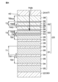
図2~図4を参照して、発光層23は、n型半導体層22の上に形成されている。発光層23は、複数の井戸層および複数の障壁層が交互に積層された多重量子井戸構造を有している。以下では、多重量子井戸構造を単に「MQW(Multiple Quantum Well)構造」という。発光層23は、より具体的には、第1MQW構造31、第2MQW構造32およびバッファMQW構造33を含む。 2 to 4, light emitting layer 23 is formed on n-type semiconductor layer 22. As shown in FIG. The light emitting layer 23 has a multiple quantum well structure in which a plurality of well layers and a plurality of barrier layers are alternately laminated. Hereinafter, the multiple quantum well structure is simply referred to as "MQW (Multiple Quantum Well) structure". Light-emitting layer 23 more specifically includes first MQW structure 31 , second MQW structure 32 and buffer MQW structure 33 .

第1MQW構造31は、n型半導体層22の上に形成されている。第1MQW構造31は、第1井戸層34および第1障壁層35が交互に積層された積層構造を有している。第1MQW構造31は、この形態では、4つの第1井戸層34および5つの第1障壁層35を含む。第1MQW構造31の最下層および最上層は、この形態では、第1障壁層35によってそれぞれ形成されている。 A first MQW structure 31 is formed on the n-type semiconductor layer 22 . The first MQW structure 31 has a laminated structure in which first well layers 34 and first barrier layers 35 are alternately laminated. The first MQW structure 31 includes four first well layers 34 and five first barrier layers 35 in this form. The bottom and top layers of the first MQW structure 31 are each formed in this form by a first barrier layer 35 .

第1井戸層34および第1障壁層35の積層数および積層順序は任意である。したがって、第1MQW構造31の最下層および/または最上層は、第1井戸層34によって形成されていてもよい。第1井戸層34および第1障壁層35は、たとえば、2以上10以下の周期で交互に積層されていてもよい。
第1井戸層34は、In組成比X(0<X<1)を有する不純物無添加のInGa(1-X)Nを含む。第1井戸層34は、410nm以上480nm未満の範囲にピーク発光波長を有する青色光を生成する青色発光層として形成されている。
The number and order of lamination of the first well layers 34 and the first barrier layers 35 are arbitrary. Therefore, the bottom layer and/or top layer of the first MQW structure 31 may be formed by the first well layer 34 . The first well layers 34 and the first barrier layers 35 may be alternately laminated with a period of 2 or more and 10 or less, for example.
The first well layer 34 contains impurity-free In X Ga (1−X) N having an In composition ratio X (0<X<1). The first well layer 34 is formed as a blue light emitting layer that generates blue light having a peak emission wavelength in the range of 410 nm or more and less than 480 nm.

In組成比Xは、0.01以上0.2以下であってもよい。In組成比Xは、0.01以上0.025以下、0.025以上0.05以下、0.05以上0.075以下、0.075以上0.1以下、0.1以上0.125以下、0.125以上0.15以下、0.15以上0.175以下、または、0.175以上0.2以下であってもよい。In組成比Xは、0.04以上0.18以下であることが好ましい。 The In composition ratio X may be 0.01 or more and 0.2 or less. In composition ratio X is 0.01 or more and 0.025 or less, 0.025 or more and 0.05 or less, 0.05 or more and 0.075 or less, 0.075 or more and 0.1 or less, 0.1 or more and 0.125 or less , 0.125 to 0.15, 0.15 to 0.175, or 0.175 to 0.2. The In composition ratio X is preferably 0.04 or more and 0.18 or less.

複数の第1井戸層34は、互いに等しいIn組成比Xを有していてもよいし、互いに異なるIn組成比Xを有していてもよい。In組成比Xが互いに等しいとは、In組成比Xが等しくなる条件下で複数の第1井戸層34が形成されていることを意味する。In組成比Xの間には、±10%程度の誤差が生じていてもよい。
複数の第1井戸層34は、この形態では、n型半導体層22から離れる方向にIn組成比Xが漸増する態様で積層されている。複数の第1井戸層34は、In組成比Xが一定の割合で漸増する態様で積層されていることが好ましい。一例として、複数の第1井戸層34は、最下の第1井戸層34から最上の第1井戸層34に向けて、In組成比Xが0.04、0.08、0.12、0.16となるように積層されていてもよい。
The plurality of first well layers 34 may have the same In composition ratio X, or may have the In composition ratio X different from each other. That the In composition ratios X are equal to each other means that the plurality of first well layers 34 are formed under the condition that the In composition ratios X are equal. An error of about ±10% may occur between the In composition ratios X.
In this embodiment, the plurality of first well layers 34 are stacked such that the In composition ratio X gradually increases in the direction away from the n-type semiconductor layer 22 . The plurality of first well layers 34 are preferably stacked in such a manner that the In composition ratio X gradually increases at a constant rate. As an example, the plurality of first well layers 34 have an In composition ratio X of 0.04, 0.08, 0.12, 0 from the bottom first well layer 34 to the top first well layer 34 . 0.16 may be stacked.

第1障壁層35は、n型不純物が添加されたGaNを含む。第1障壁層35は、n型不純物の一例としてのシリコンを含んでいてもよい。第1障壁層35の不純物濃度は、5×1016cm-3以上5×1020cm-3以下であってもよい。
第1障壁層35は、p型半導体層24から供給される正孔をn型不純物によって捕獲する。これにより、第1井戸層34に供給される正孔が減少するため、第1井戸層34における光の生成が抑制される。第1井戸層34で生成される光のピーク発光波長は、微弱(ノイズレベル)である。第1井戸層34で生成される青色光は、半導体発光層7から取り出される光のドミナント波長WL(光色)に殆ど寄与しない。
The first barrier layer 35 includes GaN doped with n-type impurities. The first barrier layer 35 may contain silicon as an example of n-type impurities. The impurity concentration of the first barrier layer 35 may be 5×10 16 cm −3 or more and 5×10 20 cm −3 or less.
The first barrier layer 35 captures holes supplied from the p-type semiconductor layer 24 by n-type impurities. As a result, the number of holes supplied to the first well layer 34 is reduced, thereby suppressing the generation of light in the first well layer 34 . The peak emission wavelength of light generated in the first well layer 34 is weak (noise level). The blue light generated in the first well layer 34 hardly contributes to the dominant wavelength WL (light color) of light extracted from the semiconductor light emitting layer 7 .

つまり、第1MQW構造31は、第1井戸層34における光の生成が第1障壁層35のn型不純物によって抑制される不活性構造(an inactive structure)を有している。第1MQW構造31は、インジウムに起因する格子サイズの変化を抑制する応力緩和構造として形成されている。
積層方向に対を成す1つの第1井戸層34および1つの第1障壁層35は、第1総厚さT1を有している。第1総厚さT1は、第1井戸層34の厚さTW1および第1障壁層35の厚さTB1の合計値(T1=TW1+TB1)である。
That is, the first MQW structure 31 has an inactive structure in which light generation in the first well layer 34 is suppressed by the n-type impurities of the first barrier layer 35 . The first MQW structure 31 is formed as a stress relaxation structure that suppresses changes in lattice size caused by indium.
One first well layer 34 and one first barrier layer 35 paired in the stacking direction have a first total thickness T1. The first total thickness T1 is the sum of the thickness TW1 of the first well layer 34 and the thickness TB1 of the first barrier layer 35 (T1=TW1+TB1).

第1井戸層34の厚さTW1は、2nm以上4nm以下であってもよい。厚さTW1は、2nm以上2.5nm以下、2.5nm以上3nm以下、3nm以上3.5nm以下、または、3.5nm以上4nm以下であってもよい。厚さTW1は、2.5nm以上3.5nm以下であることが好ましい。
複数の第1井戸層34は、互いに等しい厚さTW1を有していてもよいし、互いに異なる厚さTW1を有していてもよい。複数の第1井戸層34は、互いに等しい厚さTW1で形成されていることが好ましい。厚さTW1が互いに等しいとは、厚さTW1が等しくなる条件下で複数の第1井戸層34が形成されていることを意味する。厚さTW1の間には、±10%程度の誤差が生じていてもよい。
The thickness TW1 of the first well layer 34 may be 2 nm or more and 4 nm or less. The thickness TW1 may be 2 nm or more and 2.5 nm or less, 2.5 nm or more and 3 nm or less, 3 nm or more and 3.5 nm or less, or 3.5 nm or more and 4 nm or less. The thickness TW1 is preferably 2.5 nm or more and 3.5 nm or less.
The multiple first well layers 34 may have the same thickness TW1, or may have different thicknesses TW1. The plurality of first well layers 34 are preferably formed with the same thickness TW1. That the thicknesses TW1 are equal to each other means that the plurality of first well layers 34 are formed under the condition that the thicknesses TW1 are equal. An error of about ±10% may occur between the thicknesses TW1.

第1障壁層35の厚さTB1は、第1井戸層34の厚さTW1を超えている(TW1<TB1)。厚さTB1は、5nm以上20nm以下であってもよい。厚さTB1は、5nm以上7.5nm以下、7.5nm以上10nm以下、10nm以上12.5nm以下、12.5nm以上15nm以下、15nm以上17.5nm以下、または、17.5nm以上20nm以下であってもよい。厚さTB1は、8nm以上16nm以下であることが好ましい。 The thickness TB1 of the first barrier layer 35 exceeds the thickness TW1 of the first well layer 34 (TW1<TB1). The thickness TB1 may be 5 nm or more and 20 nm or less. The thickness TB1 is 5 nm or more and 7.5 nm or less, 7.5 nm or more and 10 nm or less, 10 nm or more and 12.5 nm or less, 12.5 nm or more and 15 nm or less, 15 nm or more and 17.5 nm or less, or 17.5 nm or more and 20 nm or less. may The thickness TB1 is preferably 8 nm or more and 16 nm or less.

複数の第1障壁層35は、互いに等しい厚さTB1を有していてもよいし、互いに異なる厚さTB1を有していてもよい。厚さTB1が互いに等しいとは、厚さTB1が等しくなる条件下で複数の第1障壁層35が形成されていることを意味する。厚さTB1の間には、±10%程度の誤差が生じていてもよい。
複数の第1障壁層35は、この形態では、最上の第1障壁層35の厚さTB1が、他の第1障壁層35の厚さTB1未満となる態様で形成されている。最上の第1障壁層35の厚さTB1は、この形態では、10nm程度である。他の第1障壁層35の厚さTB1は、この形態では、15nm程度である。このような構造は、第2MQW構造32との関係において、発光層23内の応力を緩和する上で有効である。
The multiple first barrier layers 35 may have the same thickness TB1, or may have different thicknesses TB1. That the thicknesses TB1 are equal to each other means that the plurality of first barrier layers 35 are formed under the condition that the thicknesses TB1 are equal. An error of about ±10% may occur between the thicknesses TB1.
The plurality of first barrier layers 35 are formed such that the thickness TB1 of the uppermost first barrier layer 35 is less than the thickness TB1 of the other first barrier layers 35 in this embodiment. The thickness TB1 of the uppermost first barrier layer 35 is approximately 10 nm in this embodiment. The thickness TB1 of the other first barrier layer 35 is approximately 15 nm in this embodiment. Such a structure is effective in relieving stress in the light emitting layer 23 in relation to the second MQW structure 32 .

第2MQW構造32は、第1MQW構造31の上に形成されている。第2MQW構造32は、第2井戸層36および第2障壁層37が交互に積層された積層構造を有している。第2MQW構造32は、この形態では、3つの第2井戸層36および2つの第2障壁層37を含む。第2MQW構造32の最下層は、この形態では、第2井戸層36によって形成されている。第2MQW構造32は、この形態では、第2MQW構造32の最上層を形成する最上障壁層38を含む。 A second MQW structure 32 is formed on the first MQW structure 31 . The second MQW structure 32 has a laminated structure in which second well layers 36 and second barrier layers 37 are alternately laminated. The second MQW structure 32 includes three second well layers 36 and two second barrier layers 37 in this form. The bottom layer of the second MQW structure 32 is formed by a second well layer 36 in this embodiment. The second MQW structure 32 includes a top barrier layer 38 that forms the top layer of the second MQW structure 32 in this form.

第2井戸層36および第2障壁層37の積層数および積層順序は任意である。したがって、第2MQW構造32の最下層は、第2障壁層37によって形成されていてもよい。また、第2MQW構造32の最上層は、第2井戸層36によって形成されていてもよい。第2井戸層36および第2障壁層37は、たとえば、2以上10以下の周期で交互に積層されていてもよい。ただし、第2井戸層36および第2障壁層37の積層数は、第1井戸層34および第1障壁層35の積層数未満であることが好ましい。 The number and order of lamination of the second well layers 36 and the second barrier layers 37 are arbitrary. Therefore, the bottom layer of the second MQW structure 32 may be formed by the second barrier layer 37 . Also, the top layer of the second MQW structure 32 may be formed by a second well layer 36 . The second well layers 36 and the second barrier layers 37 may be alternately laminated with a period of 2 or more and 10 or less, for example. However, the number of layers of the second well layers 36 and the second barrier layers 37 is preferably less than the number of layers of the first well layers 34 and the first barrier layers 35 .

第2井戸層36は、第1井戸層34のIn組成比Xを超えるIn組成比Y(X<Y≦1)を有する不純物無添加のInGa(1-Y)Nを含む。第2井戸層36は、480nm以上550nm以下の範囲にピーク発光波長を有する青緑色光を生成する青緑色発光層として形成されている。第2井戸層36のピーク発光波長は、より具体的には、480nm以上510nm以下である。第1井戸層34で生成される青緑色光は、半導体発光層7から取り出される光のドミナント波長WL(光色)に寄与する。 The second well layer 36 contains impurity-free In Y Ga (1−Y) 3 having an In composition ratio Y (X<Y≦1) exceeding the In composition ratio X of the first well layer 34 . The second well layer 36 is formed as a blue-green light-emitting layer that generates blue-green light having a peak emission wavelength in the range of 480 nm to 550 nm. More specifically, the peak emission wavelength of the second well layer 36 is 480 nm or more and 510 nm or less. The blue-green light generated in the first well layer 34 contributes to the dominant wavelength WL (light color) of light extracted from the semiconductor light emitting layer 7 .

In組成比Yは、0.1以上0.3以下であってもよい。In組成比Yは、0.1以上0.125以下、0.125以上0.15以下、0.15以上0.175以下、0.175以上0.2以下、0.2以上0.225以下、0.225以上0.25以下、0.25以上0.275以下、または、0.275以上0.3以下であってもよい。In組成比Yは、0.15以上0.25以下であることが好ましい。 The In composition ratio Y may be 0.1 or more and 0.3 or less. In composition ratio Y is 0.1 or more and 0.125 or less, 0.125 or more and 0.15 or less, 0.15 or more and 0.175 or less, 0.175 or more and 0.2 or less, 0.2 or more and 0.225 or less. , 0.225 to 0.25, 0.25 to 0.275, or 0.275 to 0.3. The In composition ratio Y is preferably 0.15 or more and 0.25 or less.

複数の第2井戸層36は、In組成比Yが一定となる態様で積層されている。これにより、第2井戸層36のピーク発光波長のばらつきを適切に抑制できる。一例として、複数の第2井戸層36は、全てのIn組成比Yが0.18となるように積層されていてもよい。
In組成比Yが一定であるとは、In組成比Yが一定となる条件下で複数の第2井戸層36が形成されていることを意味する。In組成比Yの間には、±10%程度の誤差が生じていてもよい。In組成比Yの誤差は、±5%以下であることが好ましい。
The plurality of second well layers 36 are laminated in such a manner that the In composition ratio Y is constant. Thereby, variations in the peak emission wavelength of the second well layer 36 can be appropriately suppressed. As an example, the plurality of second well layers 36 may be stacked such that the In composition ratio Y of all of them is 0.18.
That the In composition ratio Y is constant means that the plurality of second well layers 36 are formed under the condition that the In composition ratio Y is constant. An error of about ±10% may occur between the In composition ratios Y. The error of the In composition ratio Y is preferably ±5% or less.

複数の第2井戸層36は、互いに異なるIn組成比Yを有していてもよい。ただし、この場合、複数の第2井戸層36のピーク発光波長にばらつきが生じる点に留意する。複数の第2井戸層36は、第1MQW構造31から離れる方向にIn組成比Yが漸増する態様で積層されていてもよい。
この場合、複数の第2井戸層36は、In組成比Yが一定の割合で漸増する態様で積層されていてもよい。一例として、複数の第2井戸層36は、最下の第2井戸層36から最上の第2井戸層36に向けて、In組成比Yが0.18、0.2、0.22となるように積層されていてもよい。
The plurality of second well layers 36 may have In composition ratios Y different from each other. However, in this case, it should be noted that the peak emission wavelengths of the plurality of second well layers 36 vary. The plurality of second well layers 36 may be stacked such that the In composition ratio Y gradually increases in the direction away from the first MQW structure 31 .
In this case, the plurality of second well layers 36 may be stacked such that the In composition ratio Y gradually increases at a constant rate. As an example, the plurality of second well layers 36 have an In composition ratio Y of 0.18, 0.2, and 0.22 from the bottom second well layer 36 to the top second well layer 36. It may be laminated as follows.

第2障壁層37は、不純物無添加のGaNを含む。第2障壁層37は、p型半導体層24から供給される正孔を通過させる。これにより、第2障壁層37における正孔の消費(捕獲)が抑制されるから、第2井戸層36において光が効率的に生成される。したがって、第2MQW構造32は、第2井戸層36において光を生成する活性構造(an active structure)を有している。 The second barrier layer 37 includes undoped GaN. The second barrier layer 37 allows holes supplied from the p-type semiconductor layer 24 to pass therethrough. As a result, consumption (capture) of holes in the second barrier layer 37 is suppressed, so that light is efficiently generated in the second well layer 36 . Therefore, the second MQW structure 32 has an active structure that produces light in the second well layer 36 .

第2障壁層37は、第1MQW構造31に係る第1障壁層35のIn組成比Xを超えるIn組成比Yを有している。したがって、第2MQW構造32がn型半導体層22の上に直接形成される場合、格子サイズの急激な変化に起因して発光層23内における応力が増加する。第2MQW構造32に生じる応力は、第1MQW構造31によって緩和されている。 The second barrier layer 37 has an In composition ratio Y exceeding the In composition ratio X of the first barrier layer 35 of the first MQW structure 31 . Therefore, when the second MQW structure 32 is formed directly on the n-type semiconductor layer 22, the stress in the light emitting layer 23 increases due to the abrupt change in lattice size. A stress generated in the second MQW structure 32 is relaxed by the first MQW structure 31 .

積層方向に対を成す1つの第2井戸層36および1つの第2障壁層37は、第2総厚さT2を有している。第2総厚さT2は、第2井戸層36の厚さTW2および第2障壁層37の厚さTB2の合計値(T2=TW2+TB2)である。第2総厚さT2は、第1MQW構造31に係る第1総厚さT1未満(T2<T1)である。
第2井戸層36の厚さTW2は、第1井戸層34の厚さTW1未満(TW2<TB1)である。厚さTW2は、1nm以上2nm以下であってもよい。厚さTW2は、1nm以上1.25nm以下、1.25nm以上1.5nm以下、1.5nm以上1.75nm以下、または、1.75nm以上2nm以下であってもよい。厚さTW2は、1.5nm以上2nm以下であることが好ましい。厚さTW2は、2nm未満であることが好ましい。
One second well layer 36 and one second barrier layer 37 paired in the stacking direction have a second total thickness T2. The second total thickness T2 is the sum of the thickness TW2 of the second well layer 36 and the thickness TB2 of the second barrier layer 37 (T2=TW2+TB2). The second total thickness T2 is less than the first total thickness T1 of the first MQW structure 31 (T2<T1).
The thickness TW2 of the second well layer 36 is less than the thickness TW1 of the first well layer 34 (TW2<TB1). The thickness TW2 may be 1 nm or more and 2 nm or less. The thickness TW2 may be 1 nm or more and 1.25 nm or less, 1.25 nm or more and 1.5 nm or less, 1.5 nm or more and 1.75 nm or less, or 1.75 nm or more and 2 nm or less. The thickness TW2 is preferably 1.5 nm or more and 2 nm or less. The thickness TW2 is preferably less than 2 nm.

複数の第2井戸層36は、互いに等しい厚さTW2を有していてもよいし、互いに異なる厚さTW2を有していてもよい。複数の第2障壁層37は、互いに等しい厚さTW2で形成されていることが好ましい。厚さTW2が互いに等しいとは、厚さTW2が等しくなる条件下で複数の第2井戸層36が形成されていることを意味する。厚さTW2の間には、±10%程度の誤差が生じていてもよい。 The multiple second well layers 36 may have the same thickness TW2, or may have different thicknesses TW2. The plurality of second barrier layers 37 are preferably formed with the same thickness TW2. That the thicknesses TW2 are equal to each other means that the plurality of second well layers 36 are formed under the condition that the thicknesses TW2 are equal. An error of about ±10% may occur between the thicknesses TW2.

第2障壁層37の厚さTB2は、第2井戸層36の厚さTW2を超えている(TW2<TB2)。第2障壁層37の厚さTB2は、第1障壁層35の厚さTB1未満(TB2<TB1)である。第2障壁層37の厚さTB2は、第1障壁層35の厚さTB1の1/2以下(TB2<TB1/2)であることが好ましい。
厚さTB2は、3nm以上6nm以下であってもよい。厚さTB2は、3nm以上3.5nm以下、3.5nm以上4nm以下、4nm以上4.5nm以下、または、4.5nm以上5nm以下、5nm以上5.5nm以下、または、5.5nm以上6nm以下であってもよい。厚さTB2は、4nm以上5nm以下であることが好ましい。厚さTB2は、5nm未満であることが好ましい。
The thickness TB2 of the second barrier layer 37 exceeds the thickness TW2 of the second well layer 36 (TW2<TB2). The thickness TB2 of the second barrier layer 37 is less than the thickness TB1 of the first barrier layer 35 (TB2<TB1). The thickness TB2 of the second barrier layer 37 is preferably less than or equal to half the thickness TB1 of the first barrier layer 35 (TB2<TB1/2).
The thickness TB2 may be 3 nm or more and 6 nm or less. The thickness TB2 is 3 nm or more and 3.5 nm or less, 3.5 nm or more and 4 nm or less, 4 nm or more and 4.5 nm or less, or 4.5 nm or more and 5 nm or less, 5 nm or more and 5.5 nm or less, or 5.5 nm or more and 6 nm or less. may be The thickness TB2 is preferably 4 nm or more and 5 nm or less. Thickness TB2 is preferably less than 5 nm.

複数の第2障壁層37は、互いに等しい厚さTB2を有していてもよいし、互いに異なる厚さTB2を有していてもよい。厚さTB2が互いに等しいとは、厚さTB2が等しくなる条件下で複数の第2障壁層37が形成されていることを意味する。厚さTB2の間には、±10%程度の誤差が生じていてもよい。
最上障壁層38は、第2障壁層37の厚さTB2とは異なる厚さTBtopを有している点を除いて、第2障壁層37と同一の態様で形成されている。最上障壁層38の厚さTBtopは、第2障壁層37の厚さTB2を超えている(TB2<TBtop)。第2MQW構造32の最上層は、最上障壁層38に代えて第2障壁層37によって形成されていてもよい。
The multiple second barrier layers 37 may have the same thickness TB2, or may have different thicknesses TB2. That the thicknesses TB2 are equal to each other means that the plurality of second barrier layers 37 are formed under the condition that the thicknesses TB2 are equal. An error of about ±10% may occur between the thicknesses TB2.
The top barrier layer 38 is formed in the same manner as the second barrier layer 37 except that it has a thickness TBtop different from the thickness TB2 of the second barrier layer 37 . The thickness TBtop of the top barrier layer 38 exceeds the thickness TB2 of the second barrier layer 37 (TB2<TBtop). The top layer of the second MQW structure 32 may be formed by a second barrier layer 37 instead of the top barrier layer 38 .

バッファMQW構造33は、第1MQW構造31および第2MQW構造32の間の領域に介在されている。バッファMQW構造33は、バッファ井戸層39およびバッファ障壁層40が積層された積層構造を有している。
バッファMQW構造33は、この形態では、1つのバッファ井戸層39および1つのバッファ障壁層40を含む。バッファMQW構造33の最下層は、この形態では、バッファ井戸層39によって形成されている。バッファMQW構造33の最上層は、この形態では、バッファ障壁層40によって形成されている。
A buffer MQW structure 33 is interposed in the region between the first MQW structure 31 and the second MQW structure 32 . The buffer MQW structure 33 has a laminated structure in which a buffer well layer 39 and a buffer barrier layer 40 are laminated.
Buffer MQW structure 33 includes one buffer well layer 39 and one buffer barrier layer 40 in this form. The bottom layer of the buffer MQW structure 33 is formed by a buffer well layer 39 in this form. The top layer of the buffer MQW structure 33 is formed by a buffer barrier layer 40 in this form.

バッファ井戸層39およびバッファ障壁層40の積層数は任意である。バッファ井戸層39およびバッファ障壁層40は、たとえば、2以上10以下の周期で交互に積層されていてもよい。バッファ井戸層39およびバッファ障壁層40の積層順序は、第1MQW構造31の最上層および第2MQW構造32の最下層に応じて調整される。
第1MQW構造31の最上層が第1井戸層34によって形成されている場合、バッファMQW構造33の最下層は、バッファ障壁層40によって形成される。第1MQW構造31の最上層が第1障壁層35によって形成されている場合、バッファMQW構造33の最下層は、バッファ井戸層39によって形成される。
The number of stacks of buffer well layers 39 and buffer barrier layers 40 is arbitrary. The buffer well layers 39 and the buffer barrier layers 40 may be alternately laminated with a period of 2 or more and 10 or less, for example. The stacking order of the buffer well layers 39 and the buffer barrier layers 40 is adjusted according to the top layer of the first MQW structure 31 and the bottom layer of the second MQW structure 32 .
When the top layer of the first MQW structure 31 is formed by the first well layer 34 , the bottom layer of the buffer MQW structure 33 is formed by the buffer barrier layer 40 . When the top layer of the first MQW structure 31 is formed by the first barrier layer 35 , the bottom layer of the buffer MQW structure 33 is formed by the buffer well layer 39 .

第2MQW構造32の最下層が第2井戸層36によって形成されている場合、バッファMQW構造33の最上層は、バッファ障壁層40によって形成される。第1MQW構造31の最下層が第2障壁層37によって形成されている場合、バッファMQW構造33の最上層は、バッファ井戸層39によって形成される。
バッファ井戸層39は、第1井戸層34のIn組成比Xを超えるIn組成比Z(X<Z≦1)を有する不純物無添加のInGa(1-Z)Nを含む。バッファ井戸層39のIn組成比Zは、第2井戸層36のIn組成比Y以下(X<Z≦Y)である。
When the bottom layer of the second MQW structure 32 is formed by the second well layer 36 , the top layer of the buffer MQW structure 33 is formed by the buffer barrier layer 40 . When the bottom layer of the first MQW structure 31 is formed by the second barrier layer 37 , the top layer of the buffer MQW structure 33 is formed by the buffer well layer 39 .
The buffer well layer 39 contains impurity-free In Z Ga (1-Z) N having an In composition ratio Z (X<Z≦1) exceeding the In composition ratio X of the first well layer 34 . The In composition ratio Z of the buffer well layer 39 is less than or equal to the In composition ratio Y of the second well layer 36 (X<Z≦Y).

In組成比Zは、この形態では、In組成比Yと等しい(Z=Y)。In組成比ZがIn組成比Yと等しいとは、In組成比ZがIn組成比Yと等しくなる条件下でバッファ井戸層39が形成されていることを意味する。In組成比Zには、In組成比Yの±10%程度の誤差が生じていてもよい。
バッファ井戸層39は、480nm以上550nm以下の範囲にピーク発光波長を有する青緑色光を生成する青緑色発光層として形成されている。バッファ井戸層39のピーク発光波長は、より具体的には、480nm以上510nm以下である。
In this embodiment, the In composition ratio Z is equal to the In composition ratio Y (Z=Y). That the In composition ratio Z is equal to the In composition ratio Y means that the buffer well layer 39 is formed under the condition that the In composition ratio Z is equal to the In composition ratio Y. The In composition ratio Z may have an error of about ±10% with respect to the In composition ratio Y.
The buffer well layer 39 is formed as a blue-green light-emitting layer that generates blue-green light having a peak emission wavelength in the range of 480 nm to 550 nm. More specifically, the peak emission wavelength of the buffer well layer 39 is 480 nm or more and 510 nm or less.

In組成比Zは、0.1以上0.3以下であってもよい。In組成比Zは、0.1以上0.125以下、0.125以上0.15以下、0.15以上0.175以下、0.175以上0.2以下、0.2以上0.225以下、0.225以上0.25以下、0.25以上0.275以下、または、0.275以上0.3以下であってもよい。In組成比Zは、0.15以上0.25以下であることが好ましい。 The In composition ratio Z may be 0.1 or more and 0.3 or less. In composition ratio Z is 0.1 or more and 0.125 or less, 0.125 or more and 0.15 or less, 0.15 or more and 0.175 or less, 0.175 or more and 0.2 or less, 0.2 or more and 0.225 or less. , 0.225 to 0.25, 0.25 to 0.275, or 0.275 to 0.3. The In composition ratio Z is preferably 0.15 or more and 0.25 or less.

積層方向に隣り合う第1井戸層34およびバッファ井戸層39の間において、In組成比XおよびIn組成比Zの間の増加割合は、複数の第1井戸層34のIn組成比Xの増加割合と等しいことが好ましい。これにより、第1MQW構造31およびバッファMQW構造33の間においてIn組成比XおよびIn組成比Zの急激な変動が抑制される。
In組成比XおよびIn組成比Zの間の増加割合がIn組成比Xの増加割合と等しいとは、In組成比XおよびIn組成比Zの間の増加割合がIn組成比Xの増加割合と等しくなる条件下で、バッファ井戸層39が形成されていることを意味する。In組成比XおよびIn組成比Zの間の増加割合には、In組成比Xの増加割合の±10%程度の誤差が生じていてもよい。
Between the first well layers 34 and the buffer well layers 39 adjacent to each other in the stacking direction, the increase ratio between the In composition ratio X and the In composition ratio Z is the increase ratio of the In composition ratio X of the plurality of first well layers 34. is preferably equal to As a result, sudden changes in the In composition ratio X and the In composition ratio Z between the first MQW structure 31 and the buffer MQW structure 33 are suppressed.
That the rate of increase between the In composition ratio X and the In composition ratio Z is equal to the rate of increase of the In composition ratio X means that the rate of increase between the In composition ratio X and the In composition ratio Z is the same as the rate of increase of the In composition ratio X. It means that the buffer well layer 39 is formed under equal conditions. The rate of increase between the In composition ratio X and the In composition ratio Z may have an error of about ±10% of the rate of increase of the In composition ratio X.

バッファ障壁層40は、n型不純物が添加されたGaNを含む。バッファ障壁層40は、n型不純物の一例としてのシリコンを含んでいてもよい。バッファ障壁層40の不純物濃度は、5×1016cm-3以上5×1020cm-3以下であってもよい。
バッファ障壁層40は、p型半導体層24から供給される正孔をn型不純物によって捕獲する。これにより、バッファ井戸層39に供給される正孔が減少するため、バッファ井戸層39における光の生成が抑制される。また、第1MQW構造31に供給される正孔も減少するため、第1MQW構造31における光の生成も抑制される。
The buffer barrier layer 40 comprises GaN doped with n-type impurities. The buffer barrier layer 40 may contain silicon as an example of n-type impurities. The impurity concentration of the buffer barrier layer 40 may be 5×10 16 cm −3 or more and 5×10 20 cm −3 or less.
The buffer barrier layer 40 captures holes supplied from the p-type semiconductor layer 24 by n-type impurities. As a result, the number of holes supplied to the buffer well layer 39 is reduced, so that the generation of light in the buffer well layer 39 is suppressed. Moreover, since the number of holes supplied to the first MQW structure 31 is also reduced, the generation of light in the first MQW structure 31 is also suppressed.

バッファ井戸層39で生成される光のピーク発光波長は、微弱(ノイズレベル)である。また、バッファ井戸層39で生成されるピーク発光波長は、第2MQW構造32(第2井戸層36)で生成されるピーク発光波長と等しい。したがって、バッファ井戸層39で生成される光は、半導体発光層7から取り出される光のドミナント波長WL(光色)に影響しない。 The peak emission wavelength of light generated in the buffer well layer 39 is weak (noise level). Also, the peak emission wavelength generated by the buffer well layer 39 is equal to the peak emission wavelength generated by the second MQW structure 32 (second well layer 36). Therefore, the light generated in the buffer well layer 39 does not affect the dominant wavelength WL (light color) of the light extracted from the semiconductor light emitting layer 7. FIG.

積層方向に対を成す1つのバッファ井戸層39および1つのバッファ障壁層40は、第3総厚さT3を有している。第3総厚さT3は、バッファ井戸層39の厚さTW3およびバッファ障壁層40の厚さTB3の合計値(T3=TW3+TB3)である。
第3総厚さT3は、第1MQW構造31に係る第1総厚さT1以下(T3≦T1)である。第3総厚さT3は、第2MQW構造32に係る第2総厚さT2以上(T2≦T3)である。第3総厚さT3は、この形態では、第2総厚さT2を超えて第1総厚さT1未満(T2<T3<T1)である。
One buffer well layer 39 and one buffer barrier layer 40 paired in the stacking direction have a third total thickness T3. The third total thickness T3 is the sum of the thickness TW3 of the buffer well layer 39 and the thickness TB3 of the buffer barrier layer 40 (T3=TW3+TB3).
The third total thickness T3 is less than or equal to the first total thickness T1 (T3≦T1) of the first MQW structure 31 . The third total thickness T3 is greater than or equal to the second total thickness T2 of the second MQW structure 32 (T2≦T3). In this embodiment, the third total thickness T3 is greater than the second total thickness T2 and less than the first total thickness T1 (T2<T3<T1).

バッファ井戸層39の厚さTW3は、第2井戸層36の厚さTW2を超えている(TW2<TW3)。バッファ井戸層39の厚さTW3は、第1井戸層34の厚さTW1以下(TW3≦TW1)であることが好ましい。バッファ井戸層39の厚さTW3は、この形態では、第1井戸層34の厚さTW1と等しい(TW3=TW1)。
厚さTW3が厚さTW1と等しいとは、厚さTW3が厚さTW1と等しくなる条件下でバッファ井戸層39が形成されていることを意味する。厚さTW3には、厚さTW1の±10%程度の誤差が生じていてもよい。
The thickness TW3 of the buffer well layer 39 exceeds the thickness TW2 of the second well layer 36 (TW2<TW3). The thickness TW3 of the buffer well layer 39 is preferably equal to or less than the thickness TW1 of the first well layer 34 (TW3≤TW1). The thickness TW3 of the buffer well layer 39 is equal to the thickness TW1 of the first well layer 34 in this embodiment (TW3=TW1).
That the thickness TW3 is equal to the thickness TW1 means that the buffer well layer 39 is formed under the condition that the thickness TW3 is equal to the thickness TW1. The thickness TW3 may have an error of about ±10% of the thickness TW1.

厚さTW3は、2nm以上4nm以下であってもよい。厚さTW3は、2nm以上2.5nm以下、2.5nm以上3nm以下、3nm以上3.5nm以下、または、3.5nm以上4nm以下であってもよい。厚さTW3は、2.5nm以上3.5nm以下であることが好ましい。
バッファ障壁層40の厚さTB3は、バッファ井戸層39の厚さTW3を超えている(TW3<TB3)。バッファ障壁層40の厚さTB3は、第1障壁層35の厚さTB1以下(TB3≦TB1)である。バッファ障壁層40の厚さTB3は、第1障壁層35の厚さTB1未満(TB3<TB1)であることが好ましい。バッファ障壁層40の厚さTB3は、第1障壁層35の厚さTB1の1/2以下(TB3<TB1/2)であることがさらに好ましい。
The thickness TW3 may be 2 nm or more and 4 nm or less. The thickness TW3 may be 2 nm or more and 2.5 nm or less, 2.5 nm or more and 3 nm or less, 3 nm or more and 3.5 nm or less, or 3.5 nm or more and 4 nm or less. The thickness TW3 is preferably 2.5 nm or more and 3.5 nm or less.
The thickness TB3 of the buffer barrier layer 40 exceeds the thickness TW3 of the buffer well layer 39 (TW3<TB3). The thickness TB3 of the buffer barrier layer 40 is equal to or less than the thickness TB1 of the first barrier layer 35 (TB3≤TB1). The thickness TB3 of the buffer barrier layer 40 is preferably less than the thickness TB1 of the first barrier layer 35 (TB3<TB1). More preferably, the thickness TB3 of the buffer barrier layer 40 is less than or equal to half the thickness TB1 of the first barrier layer 35 (TB3<TB1/2).

バッファ障壁層40の厚さTB3は、第2障壁層37の厚さTB2以下(TB3≦TB2)であってもよい。バッファ障壁層40の厚さTB3は、この形態では、第2障壁層37の厚さTB2と等しい(TB3=TB2)。
厚さTB3が厚さTB2と等しいとは、厚さTB3が厚さTB2と等しくなる条件下でバッファ井戸層39が形成されていることを意味する。厚さTB3には、厚さTB2の±10%程度の誤差が生じていてもよい。
The thickness TB3 of the buffer barrier layer 40 may be less than or equal to the thickness TB2 of the second barrier layer 37 (TB3≦TB2). The thickness TB3 of the buffer barrier layer 40 is in this embodiment equal to the thickness TB2 of the second barrier layer 37 (TB3=TB2).
That thickness TB3 is equal to thickness TB2 means that buffer well layer 39 is formed under the condition that thickness TB3 is equal to thickness TB2. The thickness TB3 may have an error of about ±10% of the thickness TB2.

厚さTB3は、3nm以上6nm以下であってもよい。厚さTB3は、3nm以上3.5nm以下、3.5nm以上4nm以下、4nm以上4.5nm以下、4.5nm以上5nm以下、5nm以上5.5nm以下、または、5.5nm以上6nm以下であってもよい。厚さTB3は、4nm以上5nm以下であることが好ましい。厚さTB3は、5nm未満であることが好ましい。 The thickness TB3 may be 3 nm or more and 6 nm or less. The thickness TB3 is 3 nm or more and 3.5 nm or less, 3.5 nm or more and 4 nm or less, 4 nm or more and 4.5 nm or less, 4.5 nm or more and 5 nm or less, 5 nm or more and 5.5 nm or less, or 5.5 nm or more and 6 nm or less. may The thickness TB3 is preferably 4 nm or more and 5 nm or less. Thickness TB3 is preferably less than 5 nm.

このように、バッファMQW構造33は、第1MQW構造31の機能および第2MQW構造32の機能の双方を有している。バッファMQW構造33を第1MQW構造31および第2MQW構造32の間の領域に介在させることにより、第1MQW構造31における光の生成を適切に抑制し、第2MQW構造32において光を適切に生成させることができる。また、第1MQW構造31および第2MQW構造32の間における格子サイズの急激な変化を抑制できる。 Thus, buffer MQW structure 33 has both the function of first MQW structure 31 and the function of second MQW structure 32 . Interposing the buffer MQW structure 33 in the region between the first MQW structure 31 and the second MQW structure 32 appropriately suppresses the generation of light in the first MQW structure 31 and appropriately generates light in the second MQW structure 32. can be done. Also, rapid changes in lattice size between the first MQW structure 31 and the second MQW structure 32 can be suppressed.

複数のバッファ井戸層39が形成されている場合、複数のバッファ井戸層39は、互いに等しいIn組成比Zを有していてもよいし、互いに異なるIn組成比Zを有していてもよい。In組成比Zが互いに等しいとは、In組成比Zが等しくなる条件下で複数のバッファ井戸層39が形成されていることを意味する。In組成比Zの間には、±10%程度の誤差が生じていてもよい。 When a plurality of buffer well layers 39 are formed, the plurality of buffer well layers 39 may have the same In composition ratio Z, or may have different In composition ratios Z from each other. That the In composition ratios Z are equal to each other means that the plurality of buffer well layers 39 are formed under the condition that the In composition ratios Z are equal. An error of about ±10% may occur between the In composition ratios Z.

複数のバッファ井戸層39は、第2MQW構造32と同様に、In組成比Zが一定となる態様で積層されていてもよい。一例として、全てのバッファ井戸層39は、第2井戸層36のIn組成比Yと等しいIn組成比Zで積層されていてもよい。
複数のバッファ井戸層39は、第1MQW構造31から第2MQW構造32に向けてIn組成比Zが漸増する態様で積層されていてもよい。複数のバッファ井戸層39は、In組成比Zが一定の割合で漸増する態様で積層されていることが好ましい。
The plurality of buffer well layers 39 may be stacked in such a manner that the In composition ratio Z is constant, similar to the second MQW structure 32 . As an example, all the buffer well layers 39 may be stacked with an In composition ratio Z equal to the In composition ratio Y of the second well layers 36 .
The plurality of buffer well layers 39 may be stacked such that the In composition ratio Z gradually increases from the first MQW structure 31 toward the second MQW structure 32 . The plurality of buffer well layers 39 are preferably stacked in such a manner that the In composition ratio Z gradually increases at a constant rate.

この場合、積層方向に隣り合う第1井戸層34およびバッファ井戸層39の間において、In組成比XおよびIn組成比Zの間の増加割合は、複数の第1井戸層34のIn組成比Xの増加割合と等しいことが好ましい。
In組成比XおよびIn組成比Zの間の増加割合がIn組成比Xの増加割合と等しいとは、In組成比XおよびIn組成比Zの間の増加割合がIn組成比Xの増加割合と等しくなる条件下でバッファ井戸層39が形成されていることを意味する。In組成比XおよびIn組成比Zの間の増加割合には、In組成比Xの増加割合の±10%程度の誤差が生じていてもよい。
In this case, between the first well layers 34 and the buffer well layers 39 adjacent to each other in the stacking direction, the increase rate between the In composition ratio X and the In composition ratio Z is the In composition ratio X of the plurality of first well layers 34 is preferably equal to the increase rate of
That the rate of increase between the In composition ratio X and the In composition ratio Z is equal to the rate of increase of the In composition ratio X means that the rate of increase between the In composition ratio X and the In composition ratio Z is the same as the rate of increase of the In composition ratio X. It means that the buffer well layer 39 is formed under equal conditions. The rate of increase between the In composition ratio X and the In composition ratio Z may have an error of about ±10% of the rate of increase of the In composition ratio X.

また、積層方向に隣り合う第2井戸層36およびバッファ井戸層39の間において、In組成比YおよびIn組成比Zの間の増加割合は、複数のバッファ井戸層39のIn組成比Zの増加割合と等しいことが好ましい。
In組成比YおよびIn組成比Zの間の増加割合がIn組成比Zの増加割合と等しいとは、In組成比YおよびIn組成比Zの間の増加割合がIn組成比Zの増加割合と等しくなる条件下で第2井戸層36が形成されていることを意味する。In組成比YおよびIn組成比Zの間の増加割合には、In組成比Zの増加割合の±10%程度の誤差が生じていてもよい。
In addition, between the second well layers 36 and the buffer well layers 39 adjacent to each other in the stacking direction, the rate of increase between the In composition ratio Y and the In composition ratio Z is the increase in the In composition ratio Z of the plurality of buffer well layers 39. It is preferably equal to the percentage.
That the rate of increase between the In composition ratio Y and the In composition ratio Z is equal to the rate of increase of the In composition ratio Z means that the rate of increase between the In composition ratio Y and the In composition ratio Z is the same as the rate of increase of the In composition ratio Z. This means that the second well layer 36 is formed under equal conditions. The rate of increase between the In composition ratio Y and the In composition ratio Z may have an error of about ±10% of the rate of increase of the In composition ratio Z.

複数のバッファ井戸層39は、互いに等しい厚さTW3を有していてもよいし、互いに異なる厚さTW3を有していてもよい。複数のバッファ障壁層40は、互いに等しい厚さTB3を有していてもよいし、互いに異なる厚さTB3を有していてもよい。
図3、図5および図6を参照して、第2MQW構造32は、この形態では、第1MQW構造31に向かって窪んだ複数のリセス41が形成された主面42を有している。複数のリセス41は、第2MQW構造32の主面42に互いに間隔を空けて形成されている。複数のリセス41は、平面視において不規則なパターンで形成されている。複数のリセス41は、単位面積当たりに1×10cm-2以上1×1010cm-2以下の密度で形成されている。
The multiple buffer well layers 39 may have the same thickness TW3, or may have different thicknesses TW3. The multiple buffer barrier layers 40 may have the same thickness TB3, or may have different thicknesses TB3.
3, 5 and 6, the second MQW structure 32 in this embodiment has a main surface 42 in which a plurality of recesses 41 recessed toward the first MQW structure 31 are formed. A plurality of recesses 41 are formed on the major surface 42 of the second MQW structure 32 at intervals. A plurality of recesses 41 are formed in an irregular pattern in plan view. The plurality of recesses 41 are formed at a density of 1×10 7 cm −2 or more and 1×10 10 cm −2 or less per unit area.

複数のリセス41は、第1MQW構造31に対して第2MQW構造32側に間隔を空けて形成されていることが好ましい。複数のリセス41は、法線方向Nに関して、少なくとも1つの第2井戸層36を横切る深さを有していることが好ましい。複数のリセス41は、この形態では、法線方向Nに関して、第2MQW構造32に含まれる全ての第2井戸層36を横切る深さで形成されている。 It is preferable that the plurality of recesses 41 be spaced apart from each other on the second MQW structure 32 side with respect to the first MQW structure 31 . The plurality of recesses 41 preferably have a depth that traverses at least one second well layer 36 with respect to the normal direction N. As shown in FIG. A plurality of recesses 41 are formed with a depth across all the second well layers 36 included in the second MQW structure 32 with respect to the normal direction N in this embodiment.

複数のリセス41は、この形態では、第2MQW構造32に導入されたVピット43からなる。Vピット43は、V欠陥とも称される。Vピット43は、たとえば、基板6からの貫通転移や、発光層23内の結晶欠陥(より具体的には任意の井戸層)等を起点にして形成される。
Vピット43は、六方晶(GaN)の結晶面に対応した逆六角錐形状に形成される。Vピット43は、実際には結晶成長のばらつきを伴うため、逆円錐形状、または、逆円錐形状に近い逆六角錐形状に形成される。
A plurality of recesses 41 consist of V-pits 43 introduced in the second MQW structure 32 in this configuration. The V-pit 43 is also called a V-defect. The V pit 43 is formed starting from, for example, a threading dislocation from the substrate 6 or a crystal defect (more specifically, any well layer) in the light emitting layer 23 .
The V pits 43 are formed in an inverted hexagonal pyramidal shape corresponding to the hexagonal (GaN) crystal plane. Since the V pits 43 are actually accompanied by variations in crystal growth, they are formed in an inverted cone shape or an inverted hexagonal pyramid shape close to an inverted cone shape.

Vピット43の頂角θVは、50°以上60°以下であってもよい。頂角θVは、Vピット43を対角線に沿って切断したときに現れる頂角である。頂角θVは、50°以上52°以下、52°以上54°以下、54°以上56°以下、56°以上58°以下、または、58°以上60°以下であってもよい。頂角θVは、この形態では、55°以上57°以下である。 The apex angle θV of the V pit 43 may be 50° or more and 60° or less. The apex angle θV is the apex angle that appears when the V pit 43 is cut along the diagonal line. The apex angle θV may be 50° or more and 52° or less, 52° or more and 54° or less, 54° or more and 56° or less, 56° or more and 58° or less, or 58° or more and 60° or less. The apex angle θV is 55° or more and 57° or less in this embodiment.

Vピット43は、第2MQW構造32の主面42に対して第1MQW構造31側に下り傾斜した6個の傾斜ファセット面44A,44B,44C,44D,44E,44Fを含む。傾斜ファセット面44A~44Fは、六方晶のc面以外の面である。
傾斜ファセット面44A~44Fは、より具体的には、六方晶の半極性面によって形成されている。六方晶は6回対称であり、60°毎に等価な結晶面および等価な結晶方向を有している。したがって、各傾斜ファセット面44A~44Fは、六方晶が示す結晶対称性を有している。
The V-pit 43 includes six inclined facet surfaces 44A, 44B, 44C, 44D, 44E, and 44F inclined downward toward the first MQW structure 31 with respect to the main surface 42 of the second MQW structure 32 . The inclined facets 44A to 44F are planes other than the hexagonal c-plane.
More specifically, the inclined facet surfaces 44A to 44F are formed by hexagonal semipolar surfaces. A hexagonal crystal has 6-fold symmetry and has equivalent crystal planes and equivalent crystal directions every 60°. Therefore, each inclined facet 44A-44F has the crystal symmetry exhibited by the hexagonal crystal.

各傾斜ファセット面44A~44Fは、(1-101)面、(1-102)面、(11-22)面および(20-21)面のうちのいずれかを含んでいてもよい。つまり、各傾斜ファセット面44A~44Fは、(1-101)面に等価な結晶面、(1-102)面に等価な結晶面、(11-22)面に等価な結晶面および(20-21)面に等価な結晶面のうちのいずれかを含んでいてもよい。 Each inclined facet 44A-44F may include any of (1-101), (1-102), (11-22) and (20-21) planes. That is, each of the inclined facet planes 44A to 44F has a crystal plane equivalent to the (1-101) plane, a crystal plane equivalent to the (1-102) plane, a crystal plane equivalent to the (11-22) plane, and a (20- 21) may include any of the equivalent crystal planes.

Vピット43は、ベースVピット45、ミドルVピット46およびトップVピット47を含む。ベースVピット45は、Vピット43の導入起点となる。ベースVピット45は、この形態では、バッファMQW構造33に形成されている。ベースVピット45は、より具体的には、バッファ井戸層39を起点にしてバッファ障壁層40に形成されている。
ミドルVピット46は、ベースVピット45を起点に第2井戸層36および第2障壁層37に形成されている。第2井戸層36および第2障壁層37は、バッファ障壁層40の主面およびベースVピット45の傾斜ファセット面に倣って膜状に結晶成長されている。これにより、ミドルVピット46が、ベースVピット45を起点に第2井戸層36および第2障壁層37に形成される。
V-pits 43 include base V-pits 45 , middle V-pits 46 and top V-pits 47 . The base V pit 45 serves as an introduction starting point for the V pit 43 . A base V-pit 45 is formed in the buffer MQW structure 33 in this form. More specifically, the base V pit 45 is formed in the buffer barrier layer 40 starting from the buffer well layer 39 .
The middle V pit 46 is formed in the second well layer 36 and the second barrier layer 37 starting from the base V pit 45 . The second well layer 36 and the second barrier layer 37 are crystal-grown in a film shape following the main surface of the buffer barrier layer 40 and the inclined facet plane of the base V pit 45 . Thereby, a middle V pit 46 is formed in the second well layer 36 and the second barrier layer 37 starting from the base V pit 45 .

トップVピット47は、Vピット43の傾斜ファセット面44A~44Fを形成する。トップVピット47は、第2MQW構造32の最上障壁層38に形成されている。最上障壁層38は、第2井戸層36の主面およびミドルVピット46の傾斜ファセット面に倣って膜状に結晶成長されている。これにより、トップVピット47が、ミドルVピット46を起点に最上障壁層38に形成される。 The top V-pit 47 forms the slanted facets 44A-44F of the V-pit 43. As shown in FIG. A top V pit 47 is formed in the top barrier layer 38 of the second MQW structure 32 . The uppermost barrier layer 38 is crystal-grown as a film following the main surface of the second well layer 36 and the inclined facet surfaces of the middle V pits 46 . Thereby, a top V pit 47 is formed in the uppermost barrier layer 38 starting from the middle V pit 46 .

図2および図3を再度参照して、p型半導体層24は、発光層23の上に形成されている。p型半導体層24は、より具体的には、複数のリセス41を埋めて第2MQW構造32の主面42を被覆している。p型半導体層24は、複数のリセス41の内外の領域から第2MQW構造32に正孔を供給する。
つまり、p型半導体層24は、第2MQW構造32の主面42、および、Vピット43の傾斜ファセット面44A~44Fから第2MQW構造32に正孔を供給する。p型半導体層24は、この形態では、p型クラッド層48およびp型コンタクト層49を含む積層構造を有している。
Referring to FIGS. 2 and 3 again, p-type semiconductor layer 24 is formed on light emitting layer 23 . More specifically, the p-type semiconductor layer 24 fills the plurality of recesses 41 and covers the main surface 42 of the second MQW structure 32 . The p-type semiconductor layer 24 supplies holes to the second MQW structure 32 from regions inside and outside the plurality of recesses 41 .
That is, the p-type semiconductor layer 24 supplies holes to the second MQW structure 32 from the main surface 42 of the second MQW structure 32 and the inclined facet surfaces 44A to 44F of the V pits 43 . The p-type semiconductor layer 24 has a laminated structure including a p-type clad layer 48 and a p-type contact layer 49 in this embodiment.

p型クラッド層48は、第2MQW構造32の主面42の上に形成されている。p型クラッド層48は、より具体的には、複数のリセス41を埋めて第2MQW構造32の主面42を被覆している。p型クラッド層48は、平坦な主面を有している。p型クラッド層48は、複数のリセス41の内外の領域から第2MQW構造32に正孔を供給する。つまり、p型クラッド層48は、第2MQW構造32の主面42、および、Vピット43の傾斜ファセット面44A~44Fから第2MQW構造32に正孔を供給する。 A p-type cladding layer 48 is formed on the main surface 42 of the second MQW structure 32 . More specifically, the p-type cladding layer 48 fills the plurality of recesses 41 and covers the main surface 42 of the second MQW structure 32 . The p-type cladding layer 48 has a flat main surface. The p-type cladding layer 48 supplies holes to the second MQW structure 32 from regions inside and outside the plurality of recesses 41 . That is, the p-type cladding layer 48 supplies holes to the second MQW structure 32 from the main surface 42 of the second MQW structure 32 and the inclined facet surfaces 44A to 44F of the V pits 43 .

p型クラッド層48は、この形態では、p型不純物が添加されたGaNを含む。p型クラッド層48は、p型不純物の一例としてのマグネシウムを含んでいてもよい。p型クラッド層48のp型不純物濃度は、5×1018cm-3以上5×1020cm-3以下であってもよい。p型クラッド層48のp型不純物濃度は、この形態では、5×1019cm-3程度である。 The p-type cladding layer 48 in this form comprises GaN doped with p-type impurities. The p-type cladding layer 48 may contain magnesium as an example of p-type impurities. The p-type impurity concentration of the p-type cladding layer 48 may be 5×10 18 cm −3 or more and 5×10 20 cm −3 or less. The p-type impurity concentration of the p-type cladding layer 48 is approximately 5×10 19 cm −3 in this embodiment.

p型クラッド層48の厚さは、10nm以上50nm以下であってもよい。p型クラッド層48の厚さは、10nm以上20nm以下、20nm以上30nm以下、30nm以上40nm以下、または、40nm以上50nm以下であってもよい。p型クラッド層48の厚さは、この形態では、30nm程度である。
p型コンタクト層49は、p型クラッド層48の上に形成されている。p型コンタクト層49は、この形態では、p型不純物が添加されたGaNを含む。p型コンタクト層49は、p型不純物の一例としてのマグネシウムを含んでいてもよい。p型コンタクト層49のp型不純物濃度は、1×1018cm-3以上1×1022cm-3以下であってもよい。p型コンタクト層49のp型不純物濃度は、この形態では、2×1020cm-3程度である。
The thickness of the p-type cladding layer 48 may be 10 nm or more and 50 nm or less. The thickness of the p-type cladding layer 48 may be 10 nm or more and 20 nm or less, 20 nm or more and 30 nm or less, 30 nm or more and 40 nm or less, or 40 nm or more and 50 nm or less. The thickness of the p-type cladding layer 48 is approximately 30 nm in this embodiment.
A p-type contact layer 49 is formed on the p-type clad layer 48 . The p-type contact layer 49, in this form, comprises GaN doped with p-type impurities. The p-type contact layer 49 may contain magnesium as an example of p-type impurities. The p-type impurity concentration of the p-type contact layer 49 may be 1×10 18 cm −3 or more and 1×10 22 cm −3 or less. The p-type impurity concentration of the p-type contact layer 49 is approximately 2×10 20 cm −3 in this embodiment.

p型コンタクト層49の厚さは、50nm以上500nm以下であってもよい。p型クラッド層48の厚さは、50nm以上100nm以下、100nm以上150nm以下、150nm以上200nm以下、200nm以上250nm以下、250nm以上300nm以下、300nm以上350nm以下、350nm以上400nm以下、400nm以上450nm以下、または、450nm以上500nm以下であってもよい。p型クラッド層48の厚さは、この形態では、200nm程度である。 The thickness of the p-type contact layer 49 may be 50 nm or more and 500 nm or less. The thickness of the p-type clad layer 48 is 50 nm or more and 100 nm or less, 100 nm or more and 150 nm or less, 150 nm or more and 200 nm or less, 200 nm or more and 250 nm or less, 250 nm or more and 300 nm or less, 300 nm or more and 350 nm or less, 350 nm or more and 400 nm or less, 400 nm or more and 450 nm or less. Alternatively, it may be 450 nm or more and 500 nm or less. The thickness of the p-type clad layer 48 is approximately 200 nm in this embodiment.

図9は、ドミナント波長WL(発光波長)および順方向電流IFの関係を実測によって求めたグラフである。図9において、縦軸は半導体発光層7から取り出されるドミナント波長WL[nm]を示し、横軸は順方向電流IF[mA]を示している。
図9には、第1特性S1(破線参照)および第2特性S2(実線参照)が示されている。第1特性S1は、参考例に係る発光層23の特性を示している。第2特性S2は、この形態に係る発光層23の特性を示している。参考例に係る発光層23では、第2MQW構造32において第2井戸層36の厚さTW2が2nm以上に設定されている。
FIG. 9 is a graph obtained by actual measurement of the relationship between the dominant wavelength WL (light emission wavelength) and the forward current IF. In FIG. 9, the vertical axis indicates the dominant wavelength WL [nm] extracted from the semiconductor light emitting layer 7, and the horizontal axis indicates the forward current IF [mA].
FIG. 9 shows a first characteristic S1 (see broken line) and a second characteristic S2 (see solid line). A first characteristic S1 indicates the characteristic of the light emitting layer 23 according to the reference example. A second characteristic S2 indicates the characteristic of the light-emitting layer 23 according to this form. In the light emitting layer 23 according to the reference example, the thickness TW2 of the second well layer 36 in the second MQW structure 32 is set to 2 nm or more.

第1特性S1を参照して、参考例に係る発光層23では、順方向電流IFを0mAから200mAに変化させたとき、ドミナント波長WLが507nmから500nmまで変動した。参考例に係る発光層23では、順方向電流IFを0mAから200mAに変化させたときのドミナント波長WLの最大変化量ΔWLが5nmを超えていた。最大変化量ΔWLは、絶対値である(以下、同じ。)。 Referring to the first characteristic S1, in the light-emitting layer 23 according to the reference example, the dominant wavelength WL varied from 507 nm to 500 nm when the forward current IF was changed from 0 mA to 200 mA. In the light-emitting layer 23 according to the reference example, the maximum amount of change ΔWL in the dominant wavelength WL when the forward current IF was changed from 0 mA to 200 mA exceeded 5 nm. The maximum amount of change ΔWL is an absolute value (same below).

参考例に係る発光層23では、順方向電流IFを0mAから200mAに変化させたときのドミナント波長WLの変化率が1%を超えている。ドミナント波長WLの変化率は、より具体的には、1.3%を超えている。
順方向電流IFの増加は、発光層23に供給される正孔の増加を意味する。参考例に係る発光層23では、第2MQW構造32およびバッファMQW構造33によっては、第1MQW構造31に到達する正孔を十分に低減させることができない。そのため、順方向電流IFの増加に伴って、ドミナント波長WLが青緑色領域から青色領域側に大きくシフトした。
In the light-emitting layer 23 according to the reference example, the change rate of the dominant wavelength WL exceeds 1% when the forward current IF is changed from 0 mA to 200 mA. More specifically, the rate of change of dominant wavelength WL exceeds 1.3%.
An increase in forward current IF means an increase in holes supplied to light emitting layer 23 . In the light-emitting layer 23 according to the reference example, holes reaching the first MQW structure 31 cannot be sufficiently reduced depending on the second MQW structure 32 and the buffer MQW structure 33 . Therefore, as the forward current IF increased, the dominant wavelength WL largely shifted from the blue-green region toward the blue region.

480nm以上550nm以下(より具体的には480nm以上510nm以下)の青緑色領域の光は、色の識別性に優れているため、カラーバリアフリーへの応用もなされる。したがって、青緑色領域から青色領域側へのドミナント波長WLの変化は、色の識別性の低下を意味し、カラーバリアフリーの観点から好ましいとは言えない。
一方、第2特性S2を参照して、この形態に係る発光層23では、順方向電流IFを0mAから200mAに変化させたとき、ドミナント波長WLが506nmから504nmまで変動した。この形態に係る発光層23では、順方向電流IFを0mAから200mAに変化させたときのドミナント波長WLの最大変化量ΔWLが0nmを超えて5nm未満(より具体的には3nm未満)となった。
Since light in the bluish-green region of 480 nm to 550 nm (more specifically, 480 nm to 510 nm) has excellent color discrimination, it is also applied to color barrier-free. Therefore, the change of the dominant wavelength WL from the bluish-green region to the blue region side means a decrease in color distinguishability, and is not preferable from the viewpoint of color barrier-free.
On the other hand, referring to the second characteristic S2, in the light-emitting layer 23 according to this embodiment, the dominant wavelength WL varied from 506 nm to 504 nm when the forward current IF was changed from 0 mA to 200 mA. In the light-emitting layer 23 according to this embodiment, the maximum amount of change ΔWL in the dominant wavelength WL when the forward current IF was changed from 0 mA to 200 mA was more than 0 nm and less than 5 nm (more specifically, less than 3 nm). .

また、この形態に係る発光層23では、順方向電流IFを0mAから200mAに変化させたときのドミナント波長WLの変化率が、1%以下であった。ドミナント波長WLの変化率は、より具体的には、0.5%未満であった。
換言すると、この形態に係る発光層23では、第2井戸層36がn型半導体層22およびp型半導体層24の間を流れる順方向電流IFを0mAから200mAに変化させたときのドミナント波長WLの最大変化量ΔWLが5nm未満(より具体的には3nm未満)となる厚さを有している。
In addition, in the light-emitting layer 23 according to this embodiment, the change rate of the dominant wavelength WL was 1% or less when the forward current IF was changed from 0 mA to 200 mA. More specifically, the rate of change of dominant wavelength WL was less than 0.5%.
In other words, in the light-emitting layer 23 according to this embodiment, the dominant wavelength WL has a thickness such that the maximum change amount ΔWL of is less than 5 nm (more specifically, less than 3 nm).

また、第2井戸層36は、n型半導体層22およびp型半導体層24の間を流れる順方向電流IFを0mAから200mAに変化させたときのドミナント波長WLの変化率が1%以下となる厚さを有している。
図10は、ドミナント波長WLの最大変化量ΔWLおよび第2障壁層37の厚さTB2の関係を実測によって求めたグラフである。図10において、縦軸は半導体発光層7から取り出される光のドミナント波長WLの最大変化量ΔWL[nm]を示し、横軸は第2障壁層37の厚さTB2[nm]を示している。
Further, the second well layer 36 has a rate of change of 1% or less in the dominant wavelength WL when the forward current IF flowing between the n-type semiconductor layer 22 and the p-type semiconductor layer 24 is changed from 0 mA to 200 mA. have a thickness.
FIG. 10 is a graph obtained by actual measurement of the relationship between the maximum variation ΔWL of the dominant wavelength WL and the thickness TB2 of the second barrier layer 37. In FIG. In FIG. 10, the vertical axis indicates the maximum variation .DELTA.WL [nm] of the dominant wavelength WL of light extracted from the semiconductor light emitting layer 7, and the horizontal axis indicates the thickness TB2 [nm] of the second barrier layer 37. FIG.

図10には、第1プロット点P1、第2プロット点P2および第3プロット点P3が示されている。第1プロット点P1は、第2障壁層37の厚さTB2を10nmに設定し、順方向電流IFを5mAから20mAまで変化させた場合の最大変化量ΔWLを示している。
第2プロット点P2は、第2障壁層37の厚さTB2を7nmに設定し、順方向電流IFを5mAから20mAまで変化させた場合の最大変化量ΔWLを示している。第3プロット点P3は、第2障壁層37の厚さTB2を4.5nmに設定し、順方向電流IFを5mAから20mAまで変化させた場合の最大変化量ΔWLを示している。
FIG. 10 shows a first plotted point P1, a second plotted point P2 and a third plotted point P3. A first plotted point P1 indicates the maximum variation .DELTA.WL when the thickness TB2 of the second barrier layer 37 is set to 10 nm and the forward current IF is varied from 5 mA to 20 mA.
A second plotted point P2 indicates the maximum variation .DELTA.WL when the thickness TB2 of the second barrier layer 37 is set to 7 nm and the forward current IF is varied from 5 mA to 20 mA. A third plotted point P3 indicates the maximum variation .DELTA.WL when the thickness TB2 of the second barrier layer 37 is set to 4.5 nm and the forward current IF is varied from 5 mA to 20 mA.

第1プロット点P1を参照して、厚さTB2を10nmに設定した場合、最大変化量ΔWLは6.6nmであった。第2プロット点P2を参照して、厚さTB2を6nmに設定した場合、最大変化量ΔWLは6.3nmであった。第3プロット点P3を参照して、厚さTB2を4.5nmに設定した場合、最大変化量ΔWLは5.3nmであった。
このように、第2障壁層37の厚さTB2を小さくすることにより、最大変化量ΔWLが減少した。第2障壁層37の機能を確保すると同時に、最大変化量ΔWLの低減を図る場合、第2障壁層37の厚さTB2は、3nm以上6nm以下であることが好ましい。この場合、最大変化量ΔWLを4nm以上6.5nm以下の範囲に抑えることができる。
Referring to the first plotted point P1, when the thickness TB2 was set to 10 nm, the maximum amount of change .DELTA.WL was 6.6 nm. Referring to the second plotted point P2, when the thickness TB2 was set to 6 nm, the maximum amount of change .DELTA.WL was 6.3 nm. Referring to the third plotted point P3, when the thickness TB2 was set to 4.5 nm, the maximum amount of change .DELTA.WL was 5.3 nm.
Thus, by reducing the thickness TB2 of the second barrier layer 37, the maximum variation .DELTA.WL was reduced. In order to secure the function of the second barrier layer 37 and at the same time reduce the maximum variation ΔWL, the thickness TB2 of the second barrier layer 37 is preferably 3 nm or more and 6 nm or less. In this case, the maximum amount of change ΔWL can be suppressed within a range of 4 nm or more and 6.5 nm or less.

換言すると、第2障壁層37は、n型半導体層22およびp型半導体層24の間を流れる順方向電流IFを5mAから20mAに変化させたときのドミナント波長WLの最大変化量ΔWLが6.5nm以下となる厚さTB2を有していることが好ましい。
図1~図3を再度参照して、半導体発光層7の半導体主面13には、高域部51、低域部52および接続部53が形成されている。高域部51、低域部52および接続部53は、半導体発光層7を切り欠いて形成されている。高域部51、低域部52および接続部53は、台地状のメサ構造54を形成している。
In other words, the second barrier layer 37 has a maximum change amount ΔWL of the dominant wavelength WL of 6.5 mA when the forward current IF flowing between the n-type semiconductor layer 22 and the p-type semiconductor layer 24 is changed from 5 mA to 20 mA. It preferably has a thickness TB2 of 5 nm or less.
1 to 3, the semiconductor main surface 13 of the semiconductor light emitting layer 7 is formed with a high band portion 51, a low band portion 52 and a connecting portion 53. As shown in FIG. The high band portion 51 , the low band portion 52 and the connection portion 53 are formed by cutting the semiconductor light emitting layer 7 . The high band portion 51 , the low band portion 52 and the connection portion 53 form a plateau-shaped mesa structure 54 .

高域部51は、半導体発光層7の厚さ方向(積層方向)に関して相対的に高所に位置している。高域部51は、p型半導体層24によって形成されている。高域部51は、より具体的には、p型コンタクト層49によって形成されている。高域部51は、この形態では、平面視において半導体側面14A~14Dから間隔を空けて、半導体発光層7の中央部に形成されている。 The high region 51 is positioned relatively high with respect to the thickness direction (stacking direction) of the semiconductor light emitting layer 7 . The high band portion 51 is formed by the p-type semiconductor layer 24 . More specifically, the high region 51 is formed by the p-type contact layer 49 . In this embodiment, the high-pass portion 51 is formed in the central portion of the semiconductor light-emitting layer 7 at intervals from the semiconductor side surfaces 14A to 14D in plan view.

高域部51は、平面視において半導体側面14A~14Dに沿って平行に延びる4つの辺を有している。高域部51の平面形状は任意であり、特定の形状に限定されない。高域部51は、平面視において多角形状、円形状、楕円形状等に形成されていてもよい。
低域部52は、半導体発光層7の厚さ方向(積層方向)に関して、高域部51に対して低所に位置している。低域部52は、n型半導体層22によって形成されている。低域部52は、より具体的には、n型コンタクト層29によって形成されている。低域部52は、平面視において高域部51の周囲に沿って帯状に延びている。低域部52は、この形態では、平面視において高域部51を取り囲む無端状(環状)に形成されている。
The high band portion 51 has four sides extending in parallel along the semiconductor side surfaces 14A to 14D in plan view. The planar shape of the high band portion 51 is arbitrary, and is not limited to a specific shape. The high band portion 51 may be formed in a polygonal shape, a circular shape, an elliptical shape, or the like in plan view.
The low band portion 52 is positioned lower than the high band portion 51 with respect to the thickness direction (stacking direction) of the semiconductor light emitting layer 7 . The low-pass portion 52 is formed by the n-type semiconductor layer 22 . More specifically, the low-pass portion 52 is formed by the n-type contact layer 29 . The low frequency band portion 52 extends in a belt shape along the periphery of the high frequency band portion 51 in plan view. In this embodiment, the low frequency band portion 52 is formed in an endless shape (annular shape) surrounding the high frequency band portion 51 in plan view.

接続部53は、高域部51および低域部52を接続している。接続部53は、n型半導体層22の一部(n型コンタクト層29)、発光層23およびp型半導体層24によって形成されている。接続部53は、平面視において半導体側面14A~14Dに沿って平行に延びる4つの辺を有している。接続部53は、法線方向Nに沿って平面的に延びている。接続部53は、高域部51から低域部52に向けて下り傾斜していてもよい。 The connecting portion 53 connects the high frequency portion 51 and the low frequency portion 52 . The connection portion 53 is formed by a portion of the n-type semiconductor layer 22 (n-type contact layer 29 ), the light emitting layer 23 and the p-type semiconductor layer 24 . The connecting portion 53 has four sides extending parallel to the semiconductor side surfaces 14A to 14D in plan view. The connecting portion 53 extends in a plane along the normal direction N. As shown in FIG. The connection portion 53 may slope downward from the high frequency portion 51 toward the low frequency portion 52 .

半導体主面13の上には、接続部53を被覆する絶縁層55が形成されている。絶縁層55は、酸化シリコン層もしくは窒化シリコン層、または、酸化シリコン層および窒化シリコン層を含む積層構造を含んでいてもよい。絶縁層55は、この形態では、窒化シリコン層からなる単層構造を有している。
絶縁層55は、平面視において高域部51を取り囲んでいる。絶縁層55は、接続部53の全域を被覆している。絶縁層55は、高域部51および接続部53を接続するエッジ部を介して高域部51を被覆するオーバラップ部を含む。絶縁層55は、低域部52および接続部53を接続するエッジ部を介して低域部52を被覆するオーバラップ部を含む。
An insulating layer 55 covering the connection portion 53 is formed on the semiconductor main surface 13 . The insulating layer 55 may include a silicon oxide layer or a silicon nitride layer, or a laminated structure including a silicon oxide layer and a silicon nitride layer. The insulating layer 55 has a single-layer structure made of a silicon nitride layer in this embodiment.
The insulating layer 55 surrounds the high frequency portion 51 in plan view. The insulating layer 55 covers the entire connection portion 53 . Insulating layer 55 includes an overlap portion covering high frequency portion 51 via an edge portion connecting high frequency portion 51 and connecting portion 53 . Insulating layer 55 includes an overlap portion covering low frequency band portion 52 via an edge portion connecting low frequency band portion 52 and connecting portion 53 .

図1~図3を参照して、半導体主面13の上には、n側電極61が形成されている。n側電極61は、低域部52に配置されている。n側電極61は、低域部52において半導体側面14A~14Dのうちの少なくとも1つに沿う領域に形成されている。
n側電極61は、この形態では、低域部52における第1半導体側面14Aおよび第4半導体側面14Dを接続する角部に沿う領域に配置されている。n側電極61は、n型半導体層22(n型コンタクト層29)に電気的に接続されている。
1 to 3, an n-side electrode 61 is formed on semiconductor main surface 13. As shown in FIG. The n-side electrode 61 is arranged in the low frequency band portion 52 . The n-side electrode 61 is formed in a region along at least one of the semiconductor side surfaces 14A to 14D in the low-pass portion 52. As shown in FIG.
In this embodiment, the n-side electrode 61 is arranged in a region along the corner connecting the first semiconductor side surface 14A and the fourth semiconductor side surface 14D in the low band portion 52 . The n-side electrode 61 is electrically connected to the n-type semiconductor layer 22 (n-type contact layer 29).

n側電極61は、より具体的には、光透過電極62を含む。光透過電極62は、ITO(酸化インジウムスズ)層を含む。光透過電極62は、この形態では、ITO層からなる単層構造を有している。光透過電極62は、半導体主面13(低域部52)を被覆し、半導体発光層7で生成された光を透過させる。光透過電極62は、n型半導体層22(n型コンタクト層29)の上に形成されている。光透過電極62は、n型半導体層22(n型コンタクト層29)に電気的に接続されている。 The n-side electrode 61 more specifically includes a light transmissive electrode 62 . The light transmissive electrode 62 includes an ITO (indium tin oxide) layer. The light transmissive electrode 62 has a single layer structure made of an ITO layer in this embodiment. The light-transmissive electrode 62 covers the semiconductor main surface 13 (low-band portion 52) and allows the light generated in the semiconductor light-emitting layer 7 to pass therethrough. The light transmissive electrode 62 is formed on the n-type semiconductor layer 22 (n-type contact layer 29). The light transmissive electrode 62 is electrically connected to the n-type semiconductor layer 22 (n-type contact layer 29).

光透過電極62は、平面視において第1面積Sn1を有している。光透過電極62は、法線方向Nに沿って複数の突出部12に対向している。また、光透過電極62は、法線方向Nに沿ってバッファ層21に形成された複数の空孔25に対向している。
光透過電極62は、この形態では、本体部63および配線部64を含む。本体部63は、この形態では、平面視において円形状に形成されている。本体部63の平面形状は任意であり、特定の形状に限定されない。本体部63は、平面視において多角形状に形成されていてもよいし、楕円形状に形成されていてもよい。
The light transmissive electrode 62 has a first area Sn1 in plan view. The light-transmitting electrode 62 faces the plurality of projections 12 along the normal direction N. As shown in FIG. Also, the light-transmitting electrode 62 faces the plurality of holes 25 formed in the buffer layer 21 along the normal direction N. As shown in FIG.
The light-transmissive electrode 62 includes a body portion 63 and a wiring portion 64 in this embodiment. In this form, the body portion 63 is formed in a circular shape in plan view. The planar shape of the main body portion 63 is arbitrary and is not limited to a specific shape. The body portion 63 may be formed in a polygonal shape in plan view, or may be formed in an elliptical shape.

配線部64は、本体部63から帯状に引き出された部分である。配線部64は、この形態では、本体部63から低域部52における第1半導体側面14Aに沿う領域に引き出されている。配線部64は、平面視において高域部51を2方向、3方向または4方向から区画するように半導体側面14A~14Dのうちの2つ、3つまたは4つに沿って形成されていてもよい。 The wiring portion 64 is a strip-like portion pulled out from the main body portion 63 . In this embodiment, the wiring portion 64 is drawn out from the main body portion 63 to a region along the first semiconductor side surface 14A in the low frequency band portion 52 . The wiring portion 64 may be formed along two, three, or four of the semiconductor side surfaces 14A to 14D so as to partition the high frequency portion 51 from two, three, or four directions in plan view. good.

光透過電極62の厚さは、10nm以上500nm以下であってもよい。光透過電極62の厚さは、10nm以上100nm以下、100nm以上200nm以下、200nm以上300nm以下、300nm以上400nm以下、または、400nm以上500nm以下であってもよい。光透過電極62の厚さは、この形態では、50nm以上150nm以下である。 The thickness of the light transmissive electrode 62 may be 10 nm or more and 500 nm or less. The thickness of the light transmissive electrode 62 may be 10 nm or more and 100 nm or less, 100 nm or more and 200 nm or less, 200 nm or more and 300 nm or less, 300 nm or more and 400 nm or less, or 400 nm or more and 500 nm or less. The thickness of the light transmissive electrode 62 is 50 nm or more and 150 nm or less in this embodiment.

n側電極61は、光透過電極62の上に形成された端子電極65を含む。端子電極65は、平面視において光透過電極62の第1面積Sn1未満の第2面積Sn2(Sn2<Sn1)を有している。端子電極65は、光透過電極62の周縁から内方に間隔を空けて形成されている。
端子電極65の全域は、平面視において、光透過電極62に重なっている。端子電極65は、法線方向Nに沿って複数の突出部12に対向している。また、端子電極65は、法線方向Nに沿ってバッファ層21に形成された複数の空孔25に対向している。
The n-side electrode 61 includes a terminal electrode 65 formed on the light transmissive electrode 62 . The terminal electrode 65 has a second area Sn2 less than the first area Sn1 of the light transmissive electrode 62 (Sn2<Sn1) in plan view. The terminal electrode 65 is formed spaced inwardly from the periphery of the light transmissive electrode 62 .
The entire area of the terminal electrode 65 overlaps the light transmissive electrode 62 in plan view. The terminal electrode 65 faces the plurality of protrusions 12 along the normal direction N. As shown in FIG. In addition, the terminal electrode 65 faces the plurality of holes 25 formed in the buffer layer 21 along the normal direction N. As shown in FIG.

端子電極65は、本体部66および配線部67を含む。本体部66は、ボンディングワイヤ等の導電性接合部材が接続される部分である。本体部66は、光透過電極62の本体部63の上に配置されている。本体部66は、この形態では、平面視において円形状に形成されている。本体部66の平面形状は任意であり、特定の形状に限定されない。本体部66は、平面視において多角形状に形成されていてもよいし、楕円形状に形成されていてもよい。 Terminal electrode 65 includes main body portion 66 and wiring portion 67 . The body portion 66 is a portion to which a conductive joining member such as a bonding wire is connected. The body portion 66 is arranged on the body portion 63 of the light transmissive electrode 62 . In this form, the body portion 66 is formed in a circular shape in a plan view. The planar shape of the main body portion 66 is arbitrary and is not limited to a specific shape. The body portion 66 may be formed in a polygonal shape in plan view, or may be formed in an elliptical shape.

配線部67は、本体部66から帯状に引き出された部分である。配線部67は、光透過電極62の配線部64の上に配置されている。配線部67の引き出し態様を調整することにより、半導体発光装置1の順方向電圧VF等が調節される。
配線部67は、本体部66から低域部52における第1半導体側面14Aに沿う領域に引き出されている。配線部67は、平面視において高域部51を2方向、3方向または4方向から区画するように半導体側面14A~14Dのうちの2つ、3つまたは4つに沿って形成されていてもよい。
The wiring portion 67 is a strip-like portion drawn out from the main body portion 66 . The wiring portion 67 is arranged on the wiring portion 64 of the light transmissive electrode 62 . By adjusting the drawing mode of the wiring portion 67, the forward voltage VF and the like of the semiconductor light emitting device 1 are adjusted.
The wiring portion 67 is drawn out from the main body portion 66 to a region in the low-frequency portion 52 along the first semiconductor side surface 14A. The wiring portion 67 may be formed along two, three, or four of the semiconductor side surfaces 14A to 14D so as to partition the high frequency portion 51 from two, three, or four directions in plan view. good.

端子電極65は、断面視において頂部68、基部69、および、頂部68から基部69に向けて下り傾斜した側壁70を有する台形状に形成されている。端子電極65は、頂部68および側壁70を接続するエッジ部において外側に張り出した膨出部71を有している。
膨出部71は、法線方向Nおよび頂部68に沿う方向に向かって張り出している。膨出部71は、平面視において頂部68の周縁に沿って延びる環状に形成されている。膨出部71は、本体部66においてボンディングワイヤ等の導電性接合部材が接続される領域を画定している。
The terminal electrode 65 is formed in a trapezoidal shape having a top portion 68 , a base portion 69 , and side walls 70 inclined downward from the top portion 68 toward the base portion 69 when viewed in cross section. The terminal electrode 65 has a bulging portion 71 projecting outward at an edge portion connecting the top portion 68 and the side wall 70 .
The bulging portion 71 protrudes in the normal direction N and in a direction along the top portion 68 . The bulging portion 71 is formed in an annular shape extending along the periphery of the top portion 68 in plan view. The bulging portion 71 defines a region of the body portion 66 to which a conductive joining member such as a bonding wire is connected.

端子電極65は、この形態では、光透過電極62側からこの順に積層されたAl電極72、Ti電極73およびAu電極74を含む積層構造を有している。
Al電極72は、Al(アルミニウム)を含む。Al電極72は、純AlまたはAl合金からなる。Al合金は、AlCu合金、AlSi合金、AlSiCu合金等であってもよい。Al電極72は、この形態では、純Alからなる。
In this form, the terminal electrode 65 has a laminated structure including an Al electrode 72, a Ti electrode 73 and an Au electrode 74 laminated in this order from the light transmissive electrode 62 side.
The Al electrode 72 contains Al (aluminum). The Al electrode 72 is made of pure Al or an Al alloy. The Al alloy may be an AlCu alloy, an AlSi alloy, an AlSiCu alloy, or the like. The Al electrode 72 is made of pure Al in this form.

Al電極72は、半導体発光層7で生成された光を反射させる光反射電極として形成されている。Al電極72は、断面視において台形状に形成されている。Al電極72の側壁は、第1傾斜角θn1を有している。第1傾斜角θn1は、Al電極72の側壁が半導体主面13を基準にしてAl電極72内で成す角度である。
Al電極72の厚さは、100nm以上1500nm以下であってもよい。Al電極72の厚さは、100nm以上250nm以下、250nm以上500nm以下、500nm以上750nm以下、750nm以上1000nm以下、1000nm以上1250nm以下、または、1250nm以上1500nm以下であってもよい。Al電極72の厚さは、この形態では、250nm以上350nm以下である。Al電極72を厚くするほど、光の反射率を高めることができる。
The Al electrode 72 is formed as a light reflecting electrode that reflects light generated by the semiconductor light emitting layer 7 . The Al electrode 72 is formed in a trapezoidal shape when viewed in cross section. A side wall of the Al electrode 72 has a first inclination angle θn1. The first tilt angle θn1 is the angle formed by the sidewall of the Al electrode 72 within the Al electrode 72 with respect to the semiconductor principal surface 13 .
The thickness of the Al electrode 72 may be 100 nm or more and 1500 nm or less. The thickness of the Al electrode 72 may be 100 nm or more and 250 nm or less, 250 nm or more and 500 nm or less, 500 nm or more and 750 nm or less, 750 nm or more and 1000 nm or less, 1000 nm or more and 1250 nm or less, or 1250 nm or more and 1500 nm or less. The thickness of the Al electrode 72 is 250 nm or more and 350 nm or less in this embodiment. The thicker the Al electrode 72, the higher the reflectance of light.

Ti電極73は、Ti(チタン)を含む。Ti電極73は、Al電極72に対するAu電極74の密着力を高める接着層として形成されている。Ti電極73は、Al電極72のほぼ全域を被覆している。Ti電極73は、断面視において台形状に形成されている。Ti電極73の側壁は、Al電極72の側壁を被覆している。
Ti電極73の側壁は、Al電極72の第1傾斜角θn1を超える第2傾斜角θn2(θn1<θn2)を有している。第2傾斜角θn2は、Ti電極73の側壁が半導体主面13を基準にしてTi電極73内で成す角度である。
The Ti electrode 73 contains Ti (titanium). The Ti electrode 73 is formed as an adhesive layer that enhances the adhesion of the Au electrode 74 to the Al electrode 72 . The Ti electrode 73 covers almost the entire area of the Al electrode 72 . The Ti electrode 73 is formed in a trapezoidal shape when viewed in cross section. The sidewall of the Ti electrode 73 covers the sidewall of the Al electrode 72 .
The sidewall of the Ti electrode 73 has a second tilt angle θn2 (θn1<θn2) that exceeds the first tilt angle θn1 of the Al electrode 72 . The second tilt angle θn2 is the angle formed by the sidewall of the Ti electrode 73 within the Ti electrode 73 with respect to the semiconductor main surface 13 .

Ti電極73の厚さは、100nm以上500nm以下であってもよい。Ti電極73の厚さは、100nm以上200nm以下、200nm以上300nm以下、300nm以上400nm以下、または、400nm以上500nm以下であってもよい。Ti電極73の厚さは、この形態では、150nm以上250nm以下である。
Au電極74は、Au(金)を含む。Au電極74は、Ti電極73のほぼ全域を被覆している。Au電極74は、断面視において台形状に形成されている。Au電極74は、端子電極65の外面を形成している。Au電極74の側壁は、Ti電極73の側壁を被覆している。
The thickness of the Ti electrode 73 may be 100 nm or more and 500 nm or less. The thickness of the Ti electrode 73 may be 100 nm or more and 200 nm or less, 200 nm or more and 300 nm or less, 300 nm or more and 400 nm or less, or 400 nm or more and 500 nm or less. The thickness of the Ti electrode 73 is 150 nm or more and 250 nm or less in this embodiment.
The Au electrode 74 contains Au (gold). The Au electrode 74 covers almost the entire Ti electrode 73 . The Au electrode 74 is formed in a trapezoidal shape when viewed in cross section. The Au electrode 74 forms the outer surface of the terminal electrode 65 . The side walls of the Au electrode 74 cover the side walls of the Ti electrode 73 .

Au電極74の側壁は、Ti電極73の第2傾斜角θn2を超える第3傾斜角θn3(θn1<θn2<θn3)を有している。第3傾斜角θn3は、Au電極74の側壁が半導体主面13を基準にしてAu電極74内で成す角度である。
Au電極74の厚さは、1μm以上5μm以下であってもよい。Au電極74の厚さは、1μm以上2μm以下、2μm以上3μm以下、3μm以上4μm以下、または、4μm以上5μm以下であってもよい。Au電極74の厚さは、この形態では、1.5μm以上2.5μm以下である。
The sidewall of the Au electrode 74 has a third tilt angle θn3 (θn1<θn2<θn3) that exceeds the second tilt angle θn2 of the Ti electrode 73 . The third tilt angle θn3 is the angle formed by the side wall of the Au electrode 74 within the Au electrode 74 with respect to the semiconductor main surface 13 .
The thickness of the Au electrode 74 may be 1 μm or more and 5 μm or less. The thickness of the Au electrode 74 may be 1 μm or more and 2 μm or less, 2 μm or more and 3 μm or less, 3 μm or more and 4 μm or less, or 4 μm or more and 5 μm or less. The thickness of the Au electrode 74 is 1.5 μm or more and 2.5 μm or less in this embodiment.

図2および図7を参照して、n側電極61は、光透過電極62および端子電極65(Al電極72)の間の領域に介在するバリア電極75を含む。バリア電極75は、Al電極72のAlに起因して光透過電極62で生じるガルバニック腐食を抑制する保護電極として形成されている。これにより、ガルバニック腐食に起因する光取り出し効率の低下を抑制できる。よって、第2MQW構造32からの光を適切に取り出すことができる。 2 and 7, n-side electrode 61 includes a barrier electrode 75 interposed in a region between light transmitting electrode 62 and terminal electrode 65 (Al electrode 72). The barrier electrode 75 is formed as a protective electrode that suppresses galvanic corrosion that occurs in the light transmissive electrode 62 due to Al in the Al electrode 72 . As a result, a decrease in light extraction efficiency due to galvanic corrosion can be suppressed. Therefore, light from the second MQW structure 32 can be properly extracted.

バリア電極75は、TiN層およびCr層のうちの少なくとも一方を含む。バリア電極75は、TiN層またはCr層からなる単層構造を有していることが好ましい。Cr層は、TiN層に比べて小さい光透過率を有している。したがって、バリア電極75は、比較的大きい光透過率を有するTiN層からなることが好ましい。
バリア電極75の厚さは、光透過電極62の厚さ未満である。バリア電極75の厚さは、Al電極72の厚さ未満である。バリア電極75の厚さは、1nm以上5nm以下であってもよい。バリア電極75の厚さは、1nm以上2nm以下、2nm以上3nm以下、3nm以上4nm以下、または、4nm以上5nm以下であってもよい。バリア電極75の厚さは、この形態では、1.5nm以上2.5nm以下である。
Barrier electrode 75 includes at least one of a TiN layer and a Cr layer. The barrier electrode 75 preferably has a single layer structure consisting of a TiN layer or a Cr layer. The Cr layer has a smaller light transmittance than the TiN layer. Therefore, barrier electrode 75 is preferably made of a TiN layer having a relatively high light transmittance.
The thickness of the barrier electrode 75 is less than the thickness of the light transmissive electrode 62 . The thickness of the barrier electrode 75 is less than the thickness of the Al electrode 72 . The thickness of the barrier electrode 75 may be 1 nm or more and 5 nm or less. The thickness of the barrier electrode 75 may be 1 nm or more and 2 nm or less, 2 nm or more and 3 nm or less, 3 nm or more and 4 nm or less, or 4 nm or more and 5 nm or less. The thickness of the barrier electrode 75 is 1.5 nm or more and 2.5 nm or less in this embodiment.

バリア電極75は、平面視において光透過電極62において端子電極65が対向する領域の全域に形成されている。つまり、バリア電極75は、本体部76および配線部77を含む。バリア電極75の本体部76は、光透過電極62の本体部63および端子電極65の本体部66の間の領域に介在している。バリア電極75の配線部77は、光透過電極62の配線部64および端子電極65の配線部67の間の領域に介在している。 The barrier electrode 75 is formed over the entire area of the light transmissive electrode 62 facing the terminal electrode 65 in plan view. In other words, the barrier electrode 75 includes the body portion 76 and the wiring portion 77 . The main body portion 76 of the barrier electrode 75 is interposed in a region between the main body portion 63 of the light transmissive electrode 62 and the main body portion 66 of the terminal electrode 65 . The wiring portion 77 of the barrier electrode 75 is interposed in a region between the wiring portion 64 of the light transmissive electrode 62 and the wiring portion 67 of the terminal electrode 65 .

バリア電極75の周縁は、平面視において端子電極65の周縁に対して端子電極65の内方に位置していてもよい。バリア電極75の周縁は、端子電極65の周縁に対して面一に形成されていてもよい。バリア電極75の周縁は、平面視において端子電極65の周縁に対して端子電極65の外側に位置していてもよい。つまり、バリア電極75は、平面視において端子電極65外の領域に引き出されていてもよい。 The peripheral edge of the barrier electrode 75 may be located inside the terminal electrode 65 with respect to the peripheral edge of the terminal electrode 65 in plan view. The peripheral edge of the barrier electrode 75 may be flush with the peripheral edge of the terminal electrode 65 . The peripheral edge of the barrier electrode 75 may be positioned outside the terminal electrode 65 with respect to the peripheral edge of the terminal electrode 65 in plan view. That is, the barrier electrode 75 may be drawn out to a region outside the terminal electrode 65 in plan view.

バリア電極75は、法線方向Nに沿って複数の突出部12に対向している。また、バリア電極75は、法線方向Nに沿ってバッファ層21に形成された複数の空孔25に対向している。
図1~図3を参照して、半導体主面13の上には、p側電極81が形成されている。p側電極81は、高域部51に配置されている。p側電極81は、p型半導体層24(p型コンタクト層49)に電気的に接続されている。
The barrier electrode 75 faces the plurality of protrusions 12 along the normal direction N. As shown in FIG. Also, the barrier electrode 75 faces the plurality of holes 25 formed in the buffer layer 21 along the normal direction N. As shown in FIG.
1 to 3, p-side electrode 81 is formed on semiconductor main surface 13 . The p-side electrode 81 is arranged in the high frequency region 51 . The p-side electrode 81 is electrically connected to the p-type semiconductor layer 24 (p-type contact layer 49).

p側電極81は、より具体的には、光透過電極82を含む。光透過電極82は、ITO(酸化インジウムスズ)層を含む。光透過電極82は、この形態では、ITO層からなる単層構造を有している。光透過電極82は、半導体主面13(高域部51)を被覆し、半導体発光層7で生成された光を透過させる。光透過電極82は、p型半導体層24(p型コンタクト層49)の上に形成されている。光透過電極82は、p型半導体層24(p型コンタクト層49)に電気的に接続されている。 The p-side electrode 81 more specifically includes a light transmissive electrode 82 . The light transmissive electrode 82 includes an ITO (indium tin oxide) layer. The light transmissive electrode 82 has a single layer structure made of an ITO layer in this embodiment. The light-transmitting electrode 82 covers the semiconductor main surface 13 (high-frequency region 51 ) and transmits light generated in the semiconductor light-emitting layer 7 . The light transmissive electrode 82 is formed on the p-type semiconductor layer 24 (p-type contact layer 49). The light transmissive electrode 82 is electrically connected to the p-type semiconductor layer 24 (p-type contact layer 49).

光透過電極82は、高域部51の周縁から間隔を空けて高域部51の内方領域を被覆している。光透過電極82の周縁は、高域部51の周縁に沿って延びている。光透過電極82は、平面視において第1面積Sp1を有している。光透過電極82は、法線方向Nに沿って複数の突出部12に対向している。また、光透過電極82は、法線方向Nに沿ってバッファ層21に形成された複数の空孔25に対向している。 The light-transmitting electrode 82 covers the inner area of the high-frequency portion 51 at a distance from the periphery of the high-frequency portion 51 . A peripheral edge of the light-transmissive electrode 82 extends along a peripheral edge of the high-frequency portion 51 . The light transmissive electrode 82 has a first area Sp1 in plan view. The light-transmitting electrode 82 faces the plurality of projections 12 along the normal direction N. As shown in FIG. Also, the light-transmissive electrode 82 faces the plurality of holes 25 formed in the buffer layer 21 along the normal direction N. As shown in FIG.

光透過電極82の厚さは、10nm以上500nm以下であってもよい。光透過電極82の厚さは、10nm以上100nm以下、100nm以上200nm以下、200nm以上300nm以下、300nm以上400nm以下、または、400nm以上500nm以下であってもよい。
光透過電極82の厚さは、この形態では、50nm以上150nm以下である。光透過電極82の厚さは、n側電極61の光透過電極62の厚さと等しいことが好ましい。光透過電極82の厚さが光透過電極62の厚さと等しいとは、光透過電極82の厚さが光透過電極62の厚さと等しくなる条件下で光透過電極82が形成されていることを意味する。光透過電極82の厚さには、光透過電極62の厚さの±10%程度の誤差が生じていてもよい。
The thickness of the light transmissive electrode 82 may be 10 nm or more and 500 nm or less. The thickness of the light transmissive electrode 82 may be 10 nm or more and 100 nm or less, 100 nm or more and 200 nm or less, 200 nm or more and 300 nm or less, 300 nm or more and 400 nm or less, or 400 nm or more and 500 nm or less.
The thickness of the light transmissive electrode 82 is 50 nm or more and 150 nm or less in this embodiment. The thickness of the light transmissive electrode 82 is preferably equal to the thickness of the light transmissive electrode 62 of the n-side electrode 61 . The expression that the thickness of the light-transmitting electrode 82 is equal to the thickness of the light-transmitting electrode 62 means that the light-transmitting electrode 82 is formed under the condition that the thickness of the light-transmitting electrode 82 is equal to the thickness of the light-transmitting electrode 62 . means. The thickness of the light transmissive electrode 82 may have an error of about ±10% of the thickness of the light transmissive electrode 62 .

p側電極81は、光透過電極82の上に形成された端子電極85を含む。端子電極85は、平面視において光透過電極82の第1面積Sp1未満の第2面積Sp2(Sp2<Sp1)を有している。端子電極85は、光透過電極82の周縁から内方に間隔を空けて形成されている。
端子電極85は、平面視において光透過電極82の露出部の面積が光透過電極82の隠蔽部の面積以上となる態様で、光透過電極82の上に形成されている。これにより、端子電極85の全域は、平面視において、光透過電極82に重なっている。端子電極85は、法線方向Nに沿って複数の突出部12に対向している。また、端子電極85は、法線方向Nに沿ってバッファ層21に形成された複数の空孔25に対向している。
The p-side electrode 81 includes a terminal electrode 85 formed on the light transmissive electrode 82 . The terminal electrode 85 has a second area Sp2 (Sp2<Sp1) that is less than the first area Sp1 of the light transmissive electrode 82 in plan view. The terminal electrode 85 is formed spaced inwardly from the periphery of the light transmissive electrode 82 .
The terminal electrode 85 is formed on the light transmissive electrode 82 in such a manner that the area of the exposed portion of the light transmissive electrode 82 is greater than or equal to the area of the hidden portion of the light transmissive electrode 82 in plan view. As a result, the entire area of the terminal electrode 85 overlaps the light transmissive electrode 82 in plan view. The terminal electrode 85 faces the plurality of protrusions 12 along the normal direction N. As shown in FIG. Also, the terminal electrode 85 faces the plurality of holes 25 formed in the buffer layer 21 along the normal direction N. As shown in FIG.

端子電極85は、本体部86および配線部87を含む。本体部86は、ボンディングワイヤ等の導電性接合部材が接続される部分である。本体部86は、この形態では、平面視において円形状に形成されている。本体部86の平面形状は任意であり、特定の形状に限定されない。本体部86は、平面視において多角形状に形成されていてもよいし、楕円形状に形成されていてもよい。 Terminal electrode 85 includes main body portion 86 and wiring portion 87 . The body portion 86 is a portion to which a conductive joining member such as a bonding wire is connected. In this form, the body portion 86 is formed in a circular shape in a plan view. The planar shape of the main body portion 86 is arbitrary and is not limited to a specific shape. The body portion 86 may be formed in a polygonal shape in plan view, or may be formed in an elliptical shape.

配線部87は、本体部86から帯状に引き出された部分である。配線部87の引き出し態様を調整することにより、半導体発光装置1の順方向電圧VF等が調節される。配線部87は、この形態では、本体部86においてn側電極61に対向する部分から引き出されている。
配線部87は、この形態では、平面視において本体部86から離れる方向に湾曲した円弧状に形成され、本体部86に外接されている。配線部87は、より具体的には、異なる曲率半径を有する複数の部分を含む。複数の部分は、第1配線部87aおよび第2配線部87bを含む。
The wiring portion 87 is a strip-like portion pulled out from the main body portion 86 . The forward voltage VF and the like of the semiconductor light emitting device 1 are adjusted by adjusting the drawing mode of the wiring portion 87 . In this embodiment, the wiring portion 87 is drawn out from a portion of the body portion 86 facing the n-side electrode 61 .
In this form, the wiring portion 87 is formed in an arcuate shape curved in a direction away from the main body portion 86 in plan view, and circumscribes the main body portion 86 . The wiring portion 87 more specifically includes a plurality of portions having different radii of curvature. The multiple portions include a first wiring portion 87a and a second wiring portion 87b.

第1配線部87aは、平面視においてn側電極61(端子電極65)の本体部66を中心とする円弧状に延び、本体部86に外接されている。第2配線部87bは、平面視においてn側電極61(端子電極65)の配線部67の先端部を中心とする円弧状に延び、第1配線部87aに接続されている。
端子電極85は、断面視において頂部88、基部89、および、頂部88から基部89に向けて下り傾斜した側壁90を有する台形状に形成されている。端子電極85は、頂部88および側壁90を接続するエッジ部において膨出部91を有している。
The first wiring portion 87 a extends in an arc shape centering on the body portion 66 of the n-side electrode 61 (terminal electrode 65 ) in plan view, and is circumscribed by the body portion 86 . The second wiring portion 87b extends in an arc around the tip of the wiring portion 67 of the n-side electrode 61 (terminal electrode 65) in plan view, and is connected to the first wiring portion 87a.
The terminal electrode 85 is formed in a trapezoidal shape having a top portion 88 , a base portion 89 , and side walls 90 inclined downward from the top portion 88 toward the base portion 89 in a cross-sectional view. The terminal electrode 85 has a bulging portion 91 at an edge portion connecting the top portion 88 and the side wall 90 .

膨出部91は、法線方向Nおよび頂部88に沿う方向に向かって張り出している。膨出部91は、平面視において頂部88の周縁に沿って延びる環状に形成されている。膨出部91は、本体部86においてボンディングワイヤ等の導電性接合部材が接続される領域を画定している。
端子電極85は、この形態では、光透過電極82側からこの順に積層されたAl電極92、Ti電極93およびAu電極94を含む積層構造を有している。
The bulging portion 91 protrudes in the normal direction N and in the direction along the top portion 88 . The bulging portion 91 is formed in an annular shape extending along the periphery of the top portion 88 in plan view. The bulging portion 91 defines a region of the body portion 86 to which a conductive joining member such as a bonding wire is connected.
In this form, the terminal electrode 85 has a laminated structure including an Al electrode 92, a Ti electrode 93 and an Au electrode 94 laminated in this order from the light transmissive electrode 82 side.

Al電極92は、Al(アルミニウム)を含む。Al電極92は、純AlまたはAl合金からなっていてもよい。Al合金は、AlCu合金、AlSi合金、AlSiCu合金等であってもよい。Al電極92は、n側電極61のAl電極72と同一の電極材料からなることが好ましい。Al電極92は、この形態では、純Alからなる。
Al電極92は、半導体発光層7で生成された光を反射させる光反射電極として形成されている。Al電極92は、断面視において台形状に形成されている。Al電極92の側壁は、第1傾斜角θp1を有している。第1傾斜角θp1は、Al電極92の側壁が半導体主面13を基準にしてAl電極92内で成す角度である。
The Al electrode 92 contains Al (aluminum). The Al electrode 92 may consist of pure Al or an Al alloy. The Al alloy may be an AlCu alloy, an AlSi alloy, an AlSiCu alloy, or the like. The Al electrode 92 is preferably made of the same electrode material as the Al electrode 72 of the n-side electrode 61 . The Al electrode 92 is made of pure Al in this form.
The Al electrode 92 is formed as a light reflecting electrode that reflects light generated by the semiconductor light emitting layer 7 . The Al electrode 92 is formed in a trapezoidal shape when viewed in cross section. A side wall of the Al electrode 92 has a first inclination angle θp1. The first tilt angle θp1 is an angle formed by the sidewall of the Al electrode 92 within the Al electrode 92 with respect to the semiconductor main surface 13 .

Al電極92の厚さは、100nm以上1500nm以下であってもよい。Al電極92の厚さは、100nm以上250nm以下、250nm以上500nm以下、500nm以上750nm以下、750nm以上1000nm以下、1000nm以上1250nm以下、または、1250nm以上1500nm以下であってもよい。
Al電極92の厚さは、この形態では、250nm以上350nm以下である。Al電極92を厚くするほど、光の反射率を高めることができる。Al電極92の厚さは、n側電極61のAl電極72の厚さと等しいことが好ましい。Al電極92の厚さがAl電極72の厚さと等しいとは、Al電極92の厚さがAl電極72の厚さと等しくなる条件下でAl電極92が形成されていることを意味する。Al電極92の厚さには、Al電極72の厚さの±10%程度の誤差が生じていてもよい。
The thickness of the Al electrode 92 may be 100 nm or more and 1500 nm or less. The thickness of the Al electrode 92 may be 100 nm or more and 250 nm or less, 250 nm or more and 500 nm or less, 500 nm or more and 750 nm or less, 750 nm or more and 1000 nm or less, 1000 nm or more and 1250 nm or less, or 1250 nm or more and 1500 nm or less.
The thickness of the Al electrode 92 is 250 nm or more and 350 nm or less in this embodiment. The thicker the Al electrode 92, the higher the reflectance of light. The thickness of the Al electrode 92 is preferably equal to the thickness of the Al electrode 72 of the n-side electrode 61 . That the thickness of the Al electrode 92 is equal to the thickness of the Al electrode 72 means that the Al electrode 92 is formed under the condition that the thickness of the Al electrode 92 is equal to the thickness of the Al electrode 72 . The thickness of the Al electrode 92 may have an error of about ±10% of the thickness of the Al electrode 72 .

Ti電極93は、Ti(チタン)を含む。Ti電極93は、Al電極92に対するAu電極94の密着力を高める接着層として形成されている。Ti電極93は、Al電極92のほぼ全域を被覆している。Ti電極93は、断面視において台形状に形成されている。Ti電極93の側壁は、Al電極92の側壁を被覆している。
Ti電極93の側壁は、Al電極92の第1傾斜角θp1を超える第2傾斜角θp2(θp1<θp2)を有している。第2傾斜角θp2は、Ti電極93の側壁が半導体主面13を基準にしてTi電極93内で成す角度である。
The Ti electrode 93 contains Ti (titanium). The Ti electrode 93 is formed as an adhesive layer that enhances the adhesion of the Au electrode 94 to the Al electrode 92 . The Ti electrode 93 covers almost the entire area of the Al electrode 92 . The Ti electrode 93 is formed in a trapezoidal shape when viewed in cross section. The sidewalls of the Ti electrode 93 cover the sidewalls of the Al electrode 92 .
The side wall of the Ti electrode 93 has a second tilt angle θp2 (θp1<θp2) that exceeds the first tilt angle θp1 of the Al electrode 92 . The second tilt angle θp2 is the angle formed by the sidewall of the Ti electrode 93 within the Ti electrode 93 with respect to the semiconductor main surface 13 .

Ti電極93の厚さは、100nm以上500nm以下であってもよい。Ti電極93の厚さは、100nm以上200nm以下、200nm以上300nm以下、300nm以上400nm以下、または、400nm以上500nm以下であってもよい。
Ti電極93の厚さは、この形態では、150nm以上250nm以下である。Al電極92の厚さは、n側電極61のTi電極73の厚さと等しいことが好ましい。Ti電極93の厚さがTi電極73の厚さと等しいとは、Ti電極93の厚さがTi電極73の厚さと等しくなる条件下でTi電極93が形成されていることを意味する。Ti電極93の厚さには、Ti電極73の厚さの±10%程度の誤差が生じていてもよい。
The thickness of the Ti electrode 93 may be 100 nm or more and 500 nm or less. The thickness of the Ti electrode 93 may be 100 nm or more and 200 nm or less, 200 nm or more and 300 nm or less, 300 nm or more and 400 nm or less, or 400 nm or more and 500 nm or less.
The thickness of the Ti electrode 93 is 150 nm or more and 250 nm or less in this embodiment. The thickness of the Al electrode 92 is preferably equal to the thickness of the Ti electrode 73 of the n-side electrode 61 . That the thickness of the Ti electrode 93 is equal to the thickness of the Ti electrode 73 means that the Ti electrode 93 is formed under the condition that the thickness of the Ti electrode 93 is equal to the thickness of the Ti electrode 73 . The thickness of the Ti electrode 93 may have an error of about ±10% of the thickness of the Ti electrode 73 .

Au電極94は、Au(金)を含む。Au電極94は、Ti電極93のほぼ全域を被覆している。Au電極94は、断面視において台形状に形成されている。Au電極94は、端子電極85の外面を形成している。Au電極94の側壁は、Ti電極93の側壁を被覆している。
Au電極94の側壁は、Ti電極93の第2傾斜角θp2を超える第3傾斜角θp3(θp1<θp2<θp3)を有している。第3傾斜角θp3は、Au電極94の側壁が半導体主面13を基準にしてAu電極94内で成す角度である。
The Au electrode 94 contains Au (gold). The Au electrode 94 covers almost the entire Ti electrode 93 . The Au electrode 94 is formed in a trapezoidal shape when viewed in cross section. The Au electrode 94 forms the outer surface of the terminal electrode 85 . The side walls of the Au electrode 94 cover the side walls of the Ti electrode 93 .
The sidewall of the Au electrode 94 has a third tilt angle θp3 (θp1<θp2<θp3) that exceeds the second tilt angle θp2 of the Ti electrode 93 . The third tilt angle θp3 is the angle formed by the sidewall of the Au electrode 94 within the Au electrode 94 with respect to the semiconductor main surface 13 .

Au電極94の厚さは、1μm以上5μm以下であってもよい。Au電極94の厚さは、1μm以上2μm以下、2μm以上3μm以下、3μm以上4μm以下、または、4μm以上5μm以下であってもよい。
Au電極94の厚さは、この形態では、1.5μm以上2.5μm以下である。Au電極94の厚さは、n側電極61のAu電極74の厚さと等しいことが好ましい。Au電極94の厚さがAu電極74の厚さと等しいとは、Au電極94の厚さがAu電極74の厚さと等しくなる条件下でAu電極94が形成されていることを意味する。Au電極94の厚さには、Au電極74の厚さの±10%程度の誤差が生じていてもよい。
The thickness of the Au electrode 94 may be 1 μm or more and 5 μm or less. The thickness of the Au electrode 94 may be 1 μm or more and 2 μm or less, 2 μm or more and 3 μm or less, 3 μm or more and 4 μm or less, or 4 μm or more and 5 μm or less.
The thickness of the Au electrode 94 is 1.5 μm or more and 2.5 μm or less in this embodiment. The thickness of the Au electrode 94 is preferably equal to the thickness of the Au electrode 74 of the n-side electrode 61 . That the thickness of the Au electrode 94 is equal to the thickness of the Au electrode 74 means that the Au electrode 94 is formed under the condition that the thickness of the Au electrode 94 is equal to the thickness of the Au electrode 74 . The thickness of the Au electrode 94 may have an error of about ±10% of the thickness of the Au electrode 74 .

図3および図8を参照して、p側電極81は、光透過電極82および端子電極85(Al電極92)の間の領域に介在するバリア電極95を含む。バリア電極95は、Al電極92のAlに起因して光透過電極82で生じるガルバニック腐食を抑制する保護電極として形成されている。これにより、ガルバニック腐食に起因する光取り出し効率の低下を抑制できる。よって、第2MQW構造32からの光を適切に取り出すことができる。 3 and 8, p-side electrode 81 includes a barrier electrode 95 interposed in a region between light transmitting electrode 82 and terminal electrode 85 (Al electrode 92). The barrier electrode 95 is formed as a protective electrode that suppresses galvanic corrosion that occurs in the light transmissive electrode 82 due to Al in the Al electrode 92 . As a result, a decrease in light extraction efficiency due to galvanic corrosion can be suppressed. Therefore, light from the second MQW structure 32 can be properly extracted.

バリア電極95は、TiN層およびCr層のうちの少なくとも一方を含む。バリア電極95は、TiN層またはCr層からなる単層構造を有していることが好ましい。Cr層は、TiN層に比べて小さい光透過率を有している。したがって、バリア電極95は、比較的大きい光透過率を有するTiN層からなることが好ましい。
バリア電極95の厚さは、光透過電極82の厚さ未満である。バリア電極95の厚さは、Al電極92の厚さ未満である。バリア電極95の厚さは、1nm以上5nm以下であってもよい。バリア電極95の厚さは、1nm以上2nm以下、2nm以上3nm以下、3nm以上4nm以下、または、4nm以上5nm以下であってもよい。
Barrier electrode 95 includes at least one of a TiN layer and a Cr layer. The barrier electrode 95 preferably has a single layer structure consisting of a TiN layer or a Cr layer. The Cr layer has a smaller light transmittance than the TiN layer. Therefore, barrier electrode 95 is preferably made of a TiN layer having a relatively high light transmittance.
The thickness of the barrier electrode 95 is less than the thickness of the light transmissive electrode 82 . The thickness of the barrier electrode 95 is less than the thickness of the Al electrode 92 . The thickness of the barrier electrode 95 may be 1 nm or more and 5 nm or less. The thickness of the barrier electrode 95 may be 1 nm or more and 2 nm or less, 2 nm or more and 3 nm or less, 3 nm or more and 4 nm or less, or 4 nm or more and 5 nm or less.

バリア電極95の厚さは、この形態では、1.5nm以上2.5nm以下である。バリア電極95の厚さは、n側電極61のバリア電極75の厚さと等しいことが好ましい。バリア電極95の厚さがバリア電極75の厚さと等しいとは、バリア電極95の厚さがバリア電極75の厚さと等しくなる条件下でバリア電極95が形成されていることを意味する。バリア電極95の厚さには、バリア電極75の厚さの±10%程度の誤差が生じていてもよい。 The thickness of the barrier electrode 95 is 1.5 nm or more and 2.5 nm or less in this embodiment. The thickness of the barrier electrode 95 is preferably equal to the thickness of the barrier electrode 75 of the n-side electrode 61 . That the thickness of the barrier electrode 95 is equal to the thickness of the barrier electrode 75 means that the barrier electrode 95 is formed under the condition that the thickness of the barrier electrode 95 is equal to the thickness of the barrier electrode 75 . The thickness of the barrier electrode 95 may have an error of about ±10% of the thickness of the barrier electrode 75 .

バリア電極95は、平面視において光透過電極82において端子電極85が対向する領域の全域に形成されている。つまり、バリア電極95は、本体部96および配線部97を含む。バリア電極95の本体部96は、光透過電極82および端子電極85の本体部86の間の領域に介在している。バリア電極95の配線部97は、光透過電極62および端子電極85の配線部87の間の領域に介在している。 The barrier electrode 95 is formed over the entire area of the light transmissive electrode 82 facing the terminal electrode 85 in plan view. In other words, the barrier electrode 95 includes a body portion 96 and a wiring portion 97 . The main body portion 96 of the barrier electrode 95 is interposed in the region between the light transmissive electrode 82 and the main body portion 86 of the terminal electrode 85 . The wiring portion 97 of the barrier electrode 95 is interposed in the region between the light transmissive electrode 62 and the wiring portion 87 of the terminal electrode 85 .

バリア電極95の周縁は、平面視において端子電極85の周縁に対して端子電極85の内方に位置していてもよい。バリア電極95の周縁は、端子電極85の周縁に対して面一に形成されていてもよい。バリア電極95の周縁は、平面視において端子電極85の周縁に対して端子電極85の外側に位置していてもよい。つまり、バリア電極95は、平面視において端子電極85外の領域に引き出されていてもよい。 The peripheral edge of the barrier electrode 95 may be located inside the terminal electrode 85 with respect to the peripheral edge of the terminal electrode 85 in plan view. The peripheral edge of the barrier electrode 95 may be flush with the peripheral edge of the terminal electrode 85 . The peripheral edge of the barrier electrode 95 may be located outside the terminal electrode 85 with respect to the peripheral edge of the terminal electrode 85 in plan view. That is, the barrier electrode 95 may be drawn out to a region outside the terminal electrode 85 in plan view.

バリア電極95は、法線方向Nに沿って複数の突出部12に対向している。また、バリア電極95は、法線方向Nに沿ってバッファ層21に形成された複数の空孔25に対向している。
以上、半導体発光装置1は、n型半導体層22、発光層23、p型半導体層24を含むダブルヘテロ構造を有している。発光層23は、不活性構造を有する第1MQW構造31および活性構造を有する第2MQW構造32を含む。これにより、第1MQW構造31における光の生成を抑制し、第2MQW構造32において光を生成させることができる。
The barrier electrode 95 faces the plurality of protrusions 12 along the normal direction N. As shown in FIG. Also, the barrier electrode 95 faces the plurality of holes 25 formed in the buffer layer 21 along the normal direction N. As shown in FIG.
As described above, the semiconductor light-emitting device 1 has a double heterostructure including the n-type semiconductor layer 22 , the light-emitting layer 23 and the p-type semiconductor layer 24 . Light-emitting layer 23 includes a first MQW structure 31 having an inactive structure and a second MQW structure 32 having an active structure. As a result, light generation in the first MQW structure 31 can be suppressed, and light can be generated in the second MQW structure 32 .

第1MQW構造31は、より具体的には、In組成比X(0<X<1)を有するInGa(1-X)Nを含む第1井戸層34、および、n型不純物が添加されたGaNを含む第1障壁層35が交互に積層された積層構造を有している。積層方向に対を成す1つの第1井戸層34および1つの第1障壁層35は、第1総厚さT1を有している。
一方、第2MQW構造32は、In組成比Xを超えるIn組成比Y(X<Y≦1)を有するInGa(1-Y)Nを含む第2井戸層36、および、不純物無添加のGaNを含む第2障壁層37が交互に積層された積層構造を有している。積層方向に対を成す1つの第2井戸層36および1つの第2障壁層37は、第1総厚さT1未満の第2総厚さT2(T2<T1)を有している。
More specifically, the first MQW structure 31 includes a first well layer 34 containing In X Ga (1−X) N having an In composition ratio X (0<X<1) and an n-type impurity doped It has a laminated structure in which first barrier layers 35 containing GaN are alternately laminated. One first well layer 34 and one first barrier layer 35 paired in the stacking direction have a first total thickness T1.
On the other hand, the second MQW structure 32 includes a second well layer 36 containing In Y Ga (1−Y) N having an In composition ratio Y (X<Y≦1) exceeding the In composition ratio X, and an impurity-free It has a laminated structure in which second barrier layers 37 containing GaN are alternately laminated. One second well layer 36 and one second barrier layer 37 paired in the stacking direction have a second total thickness T2 (T2<T1) less than the first total thickness T1.

これにより、第2MQW構造32に対する正孔の供給効率を高めることができると同時に第1MQW構造31に供給される正孔を減少させることができる。その結果、第1MQW構造31における光の生成を抑制し、第2MQW構造32において光を効率的に生成させることができる。よって、順方向電流IFの変動に起因するドミナント波長WL(発光波長)の変動を抑制できる。 As a result, the efficiency of supplying holes to the second MQW structure 32 can be increased, and at the same time, the number of holes supplied to the first MQW structure 31 can be reduced. As a result, light generation in the first MQW structure 31 can be suppressed, and light can be efficiently generated in the second MQW structure 32 . Therefore, fluctuations in the dominant wavelength WL (light emission wavelength) due to fluctuations in the forward current IF can be suppressed.

第2井戸層36は、第1井戸層34の厚さTW1未満の厚さTW2(TW2<TW1)を有していることが好ましい。第2障壁層37は、第1障壁層35の厚さTB1未満の厚さTB2(TW2<TB1)を有していることが好ましい。
第1障壁層35は、第1井戸層34の厚さTW1を超える厚さTB1(TW1<TB1)を有していることが好ましい。第2障壁層37は、第2井戸層36の厚さTW2を超える厚さTB2(TW2<TB2)を有していることが好ましい。これらの構造は、順方向電流IFの変動に起因するドミナント波長WLの変動を適切に抑制する上で有効である。
The second well layer 36 preferably has a thickness TW2 that is less than the thickness TW1 of the first well layer 34 (TW2<TW1). The second barrier layer 37 preferably has a thickness TB2 that is less than the thickness TB1 of the first barrier layer 35 (TW2<TB1).
The first barrier layer 35 preferably has a thickness TB1 greater than the thickness TW1 of the first well layer 34 (TW1<TB1). The second barrier layer 37 preferably has a thickness TB2 greater than the thickness TW2 of the second well layer 36 (TW2<TB2). These structures are effective in appropriately suppressing fluctuations in dominant wavelength WL caused by fluctuations in forward current IF.

この場合、第1井戸層34は、2nm以上4nm以下の厚さを有し、第2井戸層36は、1nm以上2nm未満の厚さを有していることが好ましい。第1障壁層35は、5nm以上20nm以下の厚さを有し、第2障壁層37は、3nm以上5nm未満の厚さを有していることが好ましい。
複数の第1井戸層34は、n型半導体層22から離れる方向にIn組成比Xが漸増するように積層されていることが好ましい。これにより、インジウムに起因する格子サイズの変化を抑制できるから、第1MQW構造31内における応力を緩和できる。
In this case, the first well layer 34 preferably has a thickness of 2 nm or more and 4 nm or less, and the second well layer 36 preferably has a thickness of 1 nm or more and less than 2 nm. The first barrier layer 35 preferably has a thickness of 5 nm or more and 20 nm or less, and the second barrier layer 37 preferably has a thickness of 3 nm or more and less than 5 nm.
The plurality of first well layers 34 are preferably stacked such that the In composition ratio X gradually increases in the direction away from the n-type semiconductor layer 22 . As a result, the change in lattice size due to indium can be suppressed, so the stress in the first MQW structure 31 can be relaxed.

複数の第2井戸層36は、In組成比Yが一定となるように積層されていることが好ましい。これにより、複数の第2井戸層36におけるピーク発光波長のばらつきを抑制できるから、所望のドミナント波長WLを有する光を適切に取り出すことができる。
第2障壁層37は、第1MQW構造31に係る第1障壁層35のIn組成比Xを超えるIn組成比Yを有している。したがって、第2MQW構造32がn型半導体層22の上に直接形成される場合、格子サイズの急激な変化に起因して応力が増加する。
The plurality of second well layers 36 are preferably stacked such that the In composition ratio Y is constant. As a result, variations in peak emission wavelength in the plurality of second well layers 36 can be suppressed, so that light having a desired dominant wavelength WL can be appropriately extracted.
The second barrier layer 37 has an In composition ratio Y exceeding the In composition ratio X of the first barrier layer 35 of the first MQW structure 31 . Therefore, when the second MQW structure 32 is formed directly on the n-type semiconductor layer 22, stress increases due to the abrupt change in lattice size.

第2MQW構造32およびn型半導体層22の間に生じる応力は、第1MQW構造31によって緩和される。これにより、第2MQW構造32における格子欠陥の導入を適切に抑制できる。その結果、第2MQW構造32において所望のピーク発光波長を有する光を適切に生成できる。
また、半導体発光装置1は、第1MQW構造31および第2MQW構造32の間の領域に介在するバッファMQW構造33をさらに含む。バッファMQW構造33は、不活性構造を有している。バッファMQW構造33は、より具体的には、第1MQW構造31の機能および第2MQW構造32の機能の双方を有している。
A stress generated between the second MQW structure 32 and the n-type semiconductor layer 22 is relieved by the first MQW structure 31 . Thereby, the introduction of lattice defects in the second MQW structure 32 can be appropriately suppressed. As a result, light having a desired peak emission wavelength can be appropriately generated in the second MQW structure 32 .
Semiconductor light emitting device 1 further includes a buffer MQW structure 33 interposed in a region between first MQW structure 31 and second MQW structure 32 . Buffer MQW structure 33 has an inactive structure. The buffer MQW structure 33 more specifically has both the function of the first MQW structure 31 and the function of the second MQW structure 32 .

バッファMQW構造33は、さらに具体的には、In組成比Xを超えるIn組成比Z(X<Z≦1)を有するInGa(1-Z)Nを含むバッファ井戸層39、および、n型不純物が添加されたGaNを含むバッファ障壁層40を含む積層構造を有している。積層方向に対を成す1つのバッファ井戸層39および1つのバッファ障壁層40は、第2総厚さT2を超える第3総厚さT3(T2<T3)を有している。 More specifically, the buffer MQW structure 33 includes a buffer well layer 39 containing In Z Ga (1−Z) N having an In composition ratio Z exceeding the In composition ratio X (X<Z≦1), and n It has a layered structure including a buffer barrier layer 40 comprising doped GaN. One buffer well layer 39 and one buffer barrier layer 40 paired in the stacking direction have a third total thickness T3 (T2<T3) exceeding the second total thickness T2.

バッファ井戸層39で生成される光は、微弱である。また、バッファ井戸層39のピーク発光波長は、第2井戸層36のピーク発光波長とほぼ等しい。したがって、バッファ井戸層39で生成される光は、半導体発光層7から取り出される光のドミナント波長WL(光色)に影響を与えない。
バッファMQW構造33によれば、第1MQW構造31および第2MQW構造32の間における格子サイズの急激な変化を抑制できる。また、バッファMQW構造33によれば、第1MQW構造31における光の生成を適切に抑制できる。
Light generated in the buffer well layer 39 is weak. Also, the peak emission wavelength of the buffer well layer 39 is approximately equal to the peak emission wavelength of the second well layer 36 . Therefore, the light generated in the buffer well layer 39 does not affect the dominant wavelength WL (light color) of the light extracted from the semiconductor light emitting layer 7. FIG.
The buffer MQW structure 33 can suppress rapid changes in lattice size between the first MQW structure 31 and the second MQW structure 32 . Further, according to the buffer MQW structure 33, the generation of light in the first MQW structure 31 can be suppressed appropriately.

この場合、バッファ井戸層39は、第2井戸層36の厚さTW2を超える厚さTW3を有していることが好ましい(TW2<TW3)。また、バッファ障壁層40は、第1障壁層35の厚さTB1未満の厚さTB3を有していることが好ましい(TB3<TB1)。
また、半導体発光装置1において、第2MQW構造32は、第1MQW構造31に向かって窪んだリセス41を含む。p型半導体層24は、リセス41を埋めて第2MQW構造32を被覆し、リセス41の内外の領域において第2MQW構造32に電気的に接続されている。これにより、第2MQW構造32に正孔を効率的に供給できる。その結果、第2MQW構造32において所望のピーク発光波長を有する光を適切に生成できる。
In this case, the buffer well layer 39 preferably has a thickness TW3 that exceeds the thickness TW2 of the second well layer 36 (TW2<TW3). Also, the buffer barrier layer 40 preferably has a thickness TB3 that is less than the thickness TB1 of the first barrier layer 35 (TB3<TB1).
Also, in the semiconductor light emitting device 1 , the second MQW structure 32 includes a recess 41 recessed toward the first MQW structure 31 . The p-type semiconductor layer 24 fills the recess 41 to cover the second MQW structure 32 and is electrically connected to the second MQW structure 32 in regions inside and outside the recess 41 . Thereby, holes can be efficiently supplied to the second MQW structure 32 . As a result, light having a desired peak emission wavelength can be appropriately generated in the second MQW structure 32 .

リセス41は、第2MQW構造32の積層方向に関して、少なくとも1つの第2井戸層36を横切っていることが好ましい。リセス41は、第2MQW構造32の積層方向に関して、全ての第2井戸層36を横切っていることがさらに好ましい。これらの構造によれば、第2井戸層36に対する正孔の供給効率を適切に高めることができる。
リセス41は、第1MQW構造31に対して第2MQW構造32側に形成されていることが好ましい。このような構造によれば、第1MQW構造31に対する正孔の供給を抑制できると同時に、第2MQW構造32に対する正孔の供給効率を高めることができる。よって、リセス41が形成された構造において順方向電流IFの変動に起因するドミナント波長WLの変動を適切に抑制できる。
The recess 41 preferably crosses at least one second well layer 36 with respect to the stacking direction of the second MQW structure 32 . More preferably, the recess 41 crosses all the second well layers 36 in the stacking direction of the second MQW structure 32 . These structures can appropriately increase the efficiency of supplying holes to the second well layer 36 .
The recess 41 is preferably formed on the second MQW structure 32 side with respect to the first MQW structure 31 . According to such a structure, the supply of holes to the first MQW structure 31 can be suppressed, and at the same time, the efficiency of supplying holes to the second MQW structure 32 can be enhanced. Therefore, in the structure in which the recess 41 is formed, fluctuations in the dominant wavelength WL due to fluctuations in the forward current IF can be suppressed appropriately.

また、半導体発光装置1によれば、基板6が六方晶基板からなり、六方晶のc面に対してm軸方向に0.1°以上1°以下の角度で傾斜したオフ角を有する第1基板主面8を含む。半導体発光層7は、III族窒化物半導体層からなり、第1基板主面8の上に形成されている。これにより、良質な結晶からなる半導体発光層7を形成できる。その結果、発光層23(より具体的には、第2MQW構造32)の発光効率を高めることができる。 Further, according to the semiconductor light-emitting device 1, the substrate 6 is made of a hexagonal substrate, and the first substrate 6 has an off-angle inclined at an angle of 0.1° or more and 1° or less in the m-axis direction with respect to the c-plane of the hexagonal crystal. It includes a substrate major surface 8 . The semiconductor light emitting layer 7 is made of a Group III nitride semiconductor layer and formed on the main surface 8 of the first substrate. Thereby, the semiconductor light-emitting layer 7 made of high-quality crystals can be formed. As a result, the light emission efficiency of the light emitting layer 23 (more specifically, the second MQW structure 32) can be enhanced.

図11は、図5に対応する領域の拡大図であって、本発明の第2実施形態に係る半導体発光装置101を部分的に示す拡大図である。以下では、半導体発光装置1に対して述べた構造に対応する構造については、同一の参照符号を付して説明を省略する。
図11を参照して、複数のリセス41は、この形態では、法線方向Nに関して、第2MQW構造32の深さ方向途中部まで深さで形成されている。つまり、複数のリセス41は、バッファMQW構造33に対して第2MQW構造32側に形成されている。複数のリセス41は、Vピット43によって形成されている。
FIG. 11 is an enlarged view of a region corresponding to FIG. 5 and partially showing a semiconductor light emitting device 101 according to the second embodiment of the present invention. In the following, structures corresponding to the structures described for the semiconductor light emitting device 1 are denoted by the same reference numerals, and descriptions thereof are omitted.
Referring to FIG. 11, the plurality of recesses 41 are formed with a depth in the normal direction N up to a midpoint in the depth direction of the second MQW structure 32 in this embodiment. That is, the recesses 41 are formed on the second MQW structure 32 side with respect to the buffer MQW structure 33 . A plurality of recesses 41 are formed by V pits 43 .

Vピット43のベースVピット45は、この形態では、第2MQW構造32に形成されている。ベースVピット45は、より具体的には、最下の第2井戸層36を起点にして最下の第2障壁層37に形成されている。
Vピット43のミドルVピット46は、ベースVピット45を起点に最上障壁層38の下方に位置する第2井戸層36および第2障壁層37に形成されている。第2井戸層36および第2障壁層37は、バッファ障壁層40の主面およびベースVピット45の傾斜ファセット面に倣って膜状に結晶成長されている。これにより、ミドルVピット46が、ベースVピット45を起点に第2井戸層36および第2障壁層37に形成される。
A base V-pit 45 of V-pit 43 is formed in the second MQW structure 32 in this embodiment. More specifically, the base V pit 45 is formed in the lowermost second barrier layer 37 starting from the lowermost second well layer 36 .
A middle V pit 46 of the V pit 43 is formed in the second well layer 36 and the second barrier layer 37 located below the uppermost barrier layer 38 with the base V pit 45 as a starting point. The second well layer 36 and the second barrier layer 37 are crystal-grown in a film shape following the main surface of the buffer barrier layer 40 and the inclined facet plane of the base V pit 45 . Thereby, a middle V pit 46 is formed in the second well layer 36 and the second barrier layer 37 starting from the base V pit 45 .

Vピット43のトップVピット47は、第2MQW構造32の最上障壁層38によって形成されている。最上障壁層38は、第2井戸層36の主面およびミドルVピット46の傾斜ファセット面に倣って膜状に結晶成長されている。これにより、トップVピット47が、ミドルVピット46を起点に最上障壁層38に形成される。
以上、半導体発光装置101によっても、半導体発光装置1に対して述べた効果と同様の効果を奏することができる。また、半導体発光装置101によれば、複数のリセス41がバッファMQW構造33に対して第2MQW構造32側に形成されている。これにより、第1MQW構造31およびバッファMQW構造33における光の生成を適切に抑制できる。よって、順方向電流IFの変動に起因するドミナント波長WLの変動を適切に抑制できる。
A top V-pit 47 of V-pit 43 is formed by top barrier layer 38 of second MQW structure 32 . The uppermost barrier layer 38 is crystal-grown as a film following the main surface of the second well layer 36 and the inclined facet surfaces of the middle V pits 46 . Thereby, a top V pit 47 is formed in the uppermost barrier layer 38 starting from the middle V pit 46 .
As described above, the semiconductor light emitting device 101 can also achieve the same effects as those described for the semiconductor light emitting device 1 . Further, according to the semiconductor light emitting device 101 , the plurality of recesses 41 are formed on the second MQW structure 32 side with respect to the buffer MQW structure 33 . Thereby, generation of light in the first MQW structure 31 and the buffer MQW structure 33 can be suppressed appropriately. Therefore, fluctuations in the dominant wavelength WL due to fluctuations in the forward current IF can be suppressed appropriately.

図12は、図5に対応する領域の拡大図であって、本発明の第3実施形態に係る半導体発光装置111を部分的に示す拡大図である。以下では、半導体発光装置1に対して述べた構造に対応する構造については、同一の参照符号を付して説明を省略する。
図12を参照して、複数のリセス41は、この形態では、法線方向Nに関して、第2MQW構造32およびバッファMQW構造33を横切って第1MQW構造31に至っている。複数のリセス41は、Vピット43によって形成されている。
FIG. 12 is an enlarged view of a region corresponding to FIG. 5 and partially showing a semiconductor light emitting device 111 according to the third embodiment of the present invention. In the following, structures corresponding to the structures described for the semiconductor light emitting device 1 are denoted by the same reference numerals, and descriptions thereof are omitted.
Referring to FIG. 12, a plurality of recesses 41 extend across the second MQW structure 32 and the buffer MQW structure 33 to the first MQW structure 31 with respect to the normal direction N in this embodiment. A plurality of recesses 41 are formed by V pits 43 .

Vピット43のベースVピット45は、この形態では、第1MQW構造31の表層部に形成されている。ベースVピット45は、この形態では、最上の第1井戸層34を起点にして最上の第1障壁層35に形成されている。
Vピット43のベースVピット45は、最上の第1井戸層34から数えて2層下、3層下または4層下の第1井戸層34を起点に形成されていてもよい。ただし、正孔の注入面積を低減する観点から、ベースVピット45は、最上の第1井戸層34、または、最上の第1井戸層34から数えて2層下もしくは3層下の第1井戸層34を起点に形成されていることが好ましい。
A base V-pit 45 of the V-pit 43 is formed in the surface layer portion of the first MQW structure 31 in this embodiment. The base V pit 45 is formed in the uppermost first barrier layer 35 starting from the uppermost first well layer 34 in this embodiment.
The base V pit 45 of the V pit 43 may be formed starting from the first well layer 34 that is two, three, or four layers below the uppermost first well layer 34 . However, from the viewpoint of reducing the hole injection area, the base V pit 45 is formed in the uppermost first well layer 34 or the first well layer 2 or 3 layers below the uppermost first well layer 34 . It is preferable that the layer 34 be the starting point.

Vピット43のミドルVピット46は、ベースVピット45を起点に、バッファ井戸層39、バッファ障壁層40、第2井戸層36および第2障壁層37に形成されている。バッファ井戸層39、バッファ障壁層40、第2井戸層36および第2障壁層37は、それぞれ、最上の第1障壁層35の主面およびベースVピット45の傾斜ファセット面に倣って膜状に結晶成長されている。これにより、ミドルVピット46が、ベースVピット45を起点にバッファ井戸層39、バッファ障壁層40、第2井戸層36および第2障壁層37に形成される。 Middle V pit 46 of V pit 43 is formed in buffer well layer 39 , buffer barrier layer 40 , second well layer 36 and second barrier layer 37 starting from base V pit 45 . The buffer well layer 39, the buffer barrier layer 40, the second well layer 36 and the second barrier layer 37 are film-like following the main surface of the uppermost first barrier layer 35 and the inclined facet surface of the base V pit 45, respectively. crystal growth. Thereby, a middle V pit 46 is formed in the buffer well layer 39 , the buffer barrier layer 40 , the second well layer 36 and the second barrier layer 37 starting from the base V pit 45 .

トップVピット47は、第2MQW構造32の最上障壁層38によって形成されている。最上障壁層38は、第2井戸層36の主面およびミドルVピット46の傾斜ファセット面に倣って膜状に結晶成長されている。これにより、トップVピット47が、ミドルVピット46を起点に最上障壁層38に形成される。
以上、半導体発光装置111によれば、半導体発光装置1に対して述べた効果と同様の効果を奏することができる。また、半導体発光装置111によれば、複数のリセス41は、第2MQW構造32およびバッファMQW構造33を横切って第1MQW構造31の表層部に至っている。
Top V-pit 47 is formed by top barrier layer 38 of second MQW structure 32 . The uppermost barrier layer 38 is crystal-grown as a film following the main surface of the second well layer 36 and the inclined facet surfaces of the middle V pits 46 . Thereby, a top V pit 47 is formed in the uppermost barrier layer 38 starting from the middle V pit 46 .
As described above, according to the semiconductor light emitting device 111, the same effects as those described for the semiconductor light emitting device 1 can be obtained. Further, according to the semiconductor light emitting device 111 , the recesses 41 cross the second MQW structure 32 and the buffer MQW structure 33 to reach the surface layer of the first MQW structure 31 .

これにより、第2MQW構造32に対する正孔の供給効率を確実に高めることができる。ただし、半導体発光装置111では、第1MQW構造31およびバッファMQW構造33に供給される正孔が増加する点に留意しなければならない。
図13は、図3に対応する領域の断面図であって、本発明の第4実施形態に係る半導体発光装置121を示す断面図である。以下では、半導体発光装置1に対して述べた構造に対応する構造については、同一の参照符号を付して説明を省略する。
As a result, the efficiency of supplying holes to the second MQW structure 32 can be reliably increased. However, it should be noted that in the semiconductor light emitting device 111, the number of holes supplied to the first MQW structure 31 and the buffer MQW structure 33 increases.
FIG. 13 is a sectional view of a region corresponding to FIG. 3, showing a semiconductor light emitting device 121 according to the fourth embodiment of the present invention. In the following, structures corresponding to the structures described for the semiconductor light emitting device 1 are denoted by the same reference numerals, and descriptions thereof are omitted.

図13を参照して、半導体発光装置121に係るバッファ層21は、空孔25を有していない。以上、半導体発光装置121によれば、半導体発光装置1に対して述べた効果と同様の効果を奏することができる。第4実施形態に係るバッファ層21は、前述の第2実施形態および第3実施形態に係るバッファ層21に適用することもできる。
図14は、図3に対応する領域の断面図であって、本発明の第5実施形態に係る半導体発光装置131を示す断面図である。以下では、半導体発光装置1に対して述べた構造に対応する構造については、同一の参照符号を付して説明を省略する。
Referring to FIG. 13, buffer layer 21 in semiconductor light emitting device 121 does not have holes 25 . As described above, according to the semiconductor light emitting device 121, the same effects as those described for the semiconductor light emitting device 1 can be obtained. The buffer layer 21 according to the fourth embodiment can also be applied to the buffer layers 21 according to the above-described second and third embodiments.
FIG. 14 is a sectional view of a region corresponding to FIG. 3, showing a semiconductor light emitting device 131 according to the fifth embodiment of the present invention. In the following, structures corresponding to the structures described for the semiconductor light emitting device 1 are denoted by the same reference numerals, and descriptions thereof are omitted.

図14を参照して、半導体発光装置131に係る凹凸構造11は、この形態では、複数の突出部12に代えて、基板6の一部からなる複数の突出部132を含む。複数の突出部132は、エッチング法によって基板6の第1基板主面8を第2基板主面9に向けて選択的に掘り下げることによって形成されている。エッチング法は、ウエットエッチング法および/またはドライエッチング法であってもよい。 Referring to FIG. 14 , uneven structure 11 according to semiconductor light emitting device 131 includes a plurality of protrusions 132 formed from a portion of substrate 6 instead of protrusions 12 in this embodiment. The plurality of protrusions 132 are formed by selectively digging down the first substrate main surface 8 of the substrate 6 toward the second substrate main surface 9 by an etching method. The etching method may be a wet etching method and/or a dry etching method.

複数の突出部132は、錐台形状、ドーム形状または半球形状に形成されている。複数の突出部132は、錐台形状の一例として、円錐台形状またはn(n≧3)角錐台形状に形成されていてもよい。複数の突出部132は、互いに間隔を空けて第1基板主面8に形成されている。複数の突出部132は、平面視において行列状または千鳥状に形成されていてもよい。 The plurality of protrusions 132 are formed in a frustum shape, a dome shape, or a hemispherical shape. The plurality of projecting portions 132 may be formed in a truncated cone shape or n (n≧3) truncated pyramid shape as an example of the truncated pyramid shape. The plurality of protruding portions 132 are formed on the first substrate main surface 8 at intervals. The plurality of protrusions 132 may be formed in a matrix or zigzag pattern in plan view.

以上、半導体発光装置131によれば、半導体発光装置1に対して述べた効果と同様の効果を奏することができる。第5実施形態に係る凹凸構造11は、前述の第2実施形態、第3実施形態および第4実施形態に係る凹凸構造11に適用することもできる。
本発明はさらに他の形態でも実施できる。
前述の各実施形態では、第2MQW構造32の主面42に複数のリセス41(Vピット43)が形成された例について説明した。しかし、複数のリセス41(Vピット43)を有さない第2MQW構造32が採用されてもよい。
As described above, according to the semiconductor light emitting device 131, the same effects as those described for the semiconductor light emitting device 1 can be obtained. The concave-convex structure 11 according to the fifth embodiment can also be applied to the concave-convex structure 11 according to the above-described second, third, and fourth embodiments.
The invention can also be implemented in other forms.
In each of the embodiments described above, an example in which a plurality of recesses 41 (V pits 43) are formed in the main surface 42 of the second MQW structure 32 has been described. However, a second MQW structure 32 that does not have a plurality of recesses 41 (V-pits 43) may be employed.

前述の各実施形態では、n側電極61に係る端子電極65が、本体部66および配線部67を含む例について説明した。しかし、配線部67を有さない端子電極65が採用されてもよい。この場合、バリア電極75の配線部77は除かれてもよい。
前述の各実施形態では、p側電極81に係る端子電極85が、本体部86および配線部87を含む例について説明した。しかし、配線部87を有さない端子電極85が採用されてもよい。この場合、バリア電極95の配線部97は除かれてもよい。
In each of the above-described embodiments, an example in which the terminal electrode 65 related to the n-side electrode 61 includes the main body portion 66 and the wiring portion 67 has been described. However, a terminal electrode 65 that does not have the wiring portion 67 may be employed. In this case, the wiring portion 77 of the barrier electrode 75 may be removed.
In each of the above-described embodiments, an example in which the terminal electrode 85 related to the p-side electrode 81 includes the main body portion 86 and the wiring portion 87 has been described. However, a terminal electrode 85 that does not have the wiring portion 87 may be employed. In this case, the wiring portion 97 of the barrier electrode 95 may be removed.

前述の各実施形態では、n側電極61に係る端子電極65が、Al電極72、Ti電極73およびAu電極74を含む積層構造を有している例について説明した。しかし、端子電極65は、Al電極72からなる単層構造を有していてもよい。
前述の各実施形態において、Al電極72の上の構造は任意であり、必ずしもTi電極73およびAu電極74が積層されている必要はない。たとえば、Al電極72の上には、Ti電極73およびAu電極74に代えて、Pt(プラチナ)層や、W(タングステン)層が形成されていてもよい。
In each of the above-described embodiments, an example in which the terminal electrode 65 related to the n-side electrode 61 has a laminated structure including the Al electrode 72, the Ti electrode 73 and the Au electrode 74 has been described. However, the terminal electrode 65 may have a single layer structure consisting of the Al electrode 72 .
In each of the above-described embodiments, the structure on the Al electrode 72 is arbitrary, and the Ti electrode 73 and the Au electrode 74 do not necessarily have to be laminated. For example, a Pt (platinum) layer or a W (tungsten) layer may be formed on the Al electrode 72 instead of the Ti electrode 73 and the Au electrode 74 .

前述の各実施形態では、p側電極81に係る端子電極85が、Al電極92、Ti電極93およびAu電極94を含む積層構造を有している例について説明した。しかし、端子電極85は、Al電極92からなる単層構造を有していてもよい。
前述の各実施形態において、Al電極92の上の構造は任意であり、必ずしもTi電極93およびAu電極94が積層されている必要はない。たとえば、Al電極92の上には、Ti電極93およびAu電極94に代えて、Pt(プラチナ)層や、W(タングステン)層が形成されていてもよい。
In each of the above-described embodiments, an example in which the terminal electrode 85 related to the p-side electrode 81 has a laminated structure including the Al electrode 92, the Ti electrode 93 and the Au electrode 94 has been described. However, the terminal electrode 85 may have a single layer structure consisting of the Al electrode 92 .
In each of the above-described embodiments, the structure on the Al electrode 92 is arbitrary, and the Ti electrode 93 and the Au electrode 94 do not necessarily have to be laminated. For example, a Pt (platinum) layer or a W (tungsten) layer may be formed on the Al electrode 92 instead of the Ti electrode 93 and the Au electrode 94 .

前述の各実施形態では、第1基板主面8に凹凸構造11が形成された例について説明した。しかし、第1~第5実施形態において第1基板主面8に凹凸構造11を有さない形態が採用されてもよい。
前述の各実施形態において、各半導体部分の導電型が反転された構造が採用されてもよい。つまり、p型の部分がn型に形成され、n型の部分がp型に形成されてもよい。
In each of the above-described embodiments, an example in which the uneven structure 11 is formed on the main surface 8 of the first substrate has been described. However, in the first to fifth embodiments, a configuration in which the first substrate main surface 8 does not have the concave-convex structure 11 may be employed.
In each of the above-described embodiments, a structure in which the conductivity type of each semiconductor portion is reversed may be employed. That is, the p-type portion may be formed to be n-type, and the n-type portion may be formed to be p-type.

この明細書は、第1~第5実施形態に示された特徴の如何なる組み合わせ形態をも制限しない。第1~第5実施形態は、それらの間で任意の態様および任意の形態において組み合わせられることができる。つまり、第1~第5実施形態に示された特徴が任意の態様および任意の形態で組み合わされた半導体発光装置が採用されてもよい。
本発明の実施形態について詳細に説明してきたが、これらは本発明の技術的内容を明らかにするために用いられた具体例に過ぎず、本発明はこれらの具体例に限定して解釈されるべきではなく、本発明の範囲は添付の請求の範囲によってのみ限定される。
This specification does not limit any combination of features shown in the first to fifth embodiments. The first to fifth embodiments can be combined in any manner and in any form among them. In other words, a semiconductor light-emitting device in which the features shown in the first to fifth embodiments are combined in any manner and in any form may be employed.
Although the embodiments of the present invention have been described in detail, these are merely specific examples used to clarify the technical content of the present invention, and the present invention should be construed as being limited to these specific examples. should not, the scope of the invention is limited only by the appended claims.

1 半導体発光装置
22 n型半導体層
24 p型半導体層
31 第1MQW構造
32 第2MQW構造
33 バッファMQW構造
34 第1井戸層
35 第1障壁層
36 第2井戸層
37 第2障壁層
39 バッファ井戸層
40 バッファ障壁層
41 リセス
101 半導体発光装置
111 半導体発光装置
121 半導体発光装置
131 半導体発光装置
T1 第1総厚さ
T2 第2総厚さ
T3 第3総厚さ
TB1 第1障壁層の厚さ
TB2 第2障壁層の厚さ
TB3 バッファ障壁層の厚さ
TW1 第1井戸層の厚さ
TW2 第2井戸層の厚さ
TW3 バッファ井戸層の厚さ
WL ドミナント波長
X In組成比
Y In組成比
Z In組成比
1 semiconductor light emitting device 22 n-type semiconductor layer 24 p-type semiconductor layer 31 first MQW structure 32 second MQW structure 33 buffer MQW structure 34 first well layer 35 first barrier layer 36 second well layer 37 second barrier layer 39 buffer well layer 40 buffer barrier layer 41 recess 101 semiconductor light emitting device 111 semiconductor light emitting device 121 semiconductor light emitting device 131 semiconductor light emitting device T1 first total thickness T2 second total thickness T3 third total thickness TB1 first barrier layer thickness TB2 2 Barrier layer thickness TB3 Buffer barrier layer thickness TW1 First well layer thickness TW2 Second well layer thickness TW3 Buffer well layer thickness WL Dominant wavelength X In composition ratio Y In composition ratio Z In composition ratio

Claims (19)

第1導電型の第1半導体層と、
In組成比X(0<X<1)を有するInGa(1-X)Nを含む第1井戸層、および、第1導電型不純物が添加されたGaNを含む第1障壁層が交互に積層され、対を成す前記第1井戸層および前記第1障壁層が第1総厚さを有する積層構造を有し、前記第1半導体層の上に形成された第1MQW構造と、
前記In組成比Xを超えるIn組成比Y(X<Y≦1)を有するInGa(1-Y)Nを含む第2井戸層、および、不純物無添加のGaNを含む第2障壁層が交互に積層され、対を成す前記第2井戸層および前記第2障壁層が前記第1総厚さ未満の第2総厚さを有する積層構造を有し、前記第1MQW構造の上に形成された第2MQW構造と、
前記第2MQW構造の上に形成された第2導電型の第2半導体層と、
前記In組成比Xを超えるIn組成比Z(X<Z≦1)を有するIn Ga (1-Z) Nを含むバッファ井戸層、および、第1導電型不純物が添加されたGaNを含むバッファ障壁層を含み、対を成す前記バッファ井戸層および前記バッファ障壁層が前記第2総厚さを超える第3総厚さを有する積層構造を有し、前記第1MQW構造および前記第2MQW構造の間の領域に介在するバッファMQW構造と、を含み、
前記第1MQW構造は、前記第1半導体層から離れる方向に前記In組成比Xが漸増するように積層された複数の前記第1井戸層を含み、
前記第2MQW構造は、前記In組成比Yが一定となるように積層された複数の前記第2井戸層を含み、
積層方向に隣り合う前記第1井戸層および前記バッファ井戸層の間において、前記In組成比Xおよび前記In組成比Zの間の増加割合は、複数の前記第1井戸層の前記In組成比Xの増加割合と等しい、半導体発光装置。
a first semiconductor layer of a first conductivity type;
Alternating first well layers containing In X Ga (1−X) N having an In composition ratio X (0<X<1) and first barrier layers containing GaN doped with first conductivity type impurities a first MQW structure formed on the first semiconductor layer, the stacked first well layer and the first barrier layer forming a pair having a stacked structure having a first total thickness;
A second well layer containing In Y Ga (1−Y) N having an In composition ratio Y (X<Y≦1) exceeding the In composition ratio X, and a second barrier layer containing GaN with no impurity added. A stacked structure in which the second well layers and the second barrier layers are alternately stacked to form a pair and have a second total thickness less than the first total thickness, and are formed on the first MQW structure. a second MQW structure;
a second conductivity type second semiconductor layer formed on the second MQW structure;
A buffer well layer containing In Z Ga (1-Z) N having an In composition ratio Z (X<Z≦1) exceeding the In composition ratio X, and a buffer containing GaN doped with first conductivity type impurities a stacked structure including barrier layers, wherein the buffer well layer paired with the buffer barrier layer has a third total thickness greater than the second total thickness, and between the first MQW structure and the second MQW structure; a buffer MQW structure intervening in the region of
The first MQW structure includes a plurality of first well layers stacked such that the In composition ratio X gradually increases in a direction away from the first semiconductor layer,
The second MQW structure includes a plurality of second well layers stacked such that the In composition ratio Y is constant,
Between the first well layers and the buffer well layers adjacent to each other in the stacking direction, the rate of increase between the In composition ratio X and the In composition ratio Z is equal to the In composition ratio X of the plurality of first well layers. A semiconductor light-emitting device equal to the increasing rate of .
前記バッファ井戸層の前記In組成比Zは、前記第2井戸層の前記In組成比Y以下(X<Z≦Y)である、請求項1に記載の半導体発光装置。2. The semiconductor light emitting device according to claim 1, wherein said In composition ratio Z of said buffer well layer is equal to or less than said In composition ratio Y of said second well layer (X<Z≤Y). 前記バッファMQW構造は、前記第1MQW構造から前記第2MQW構造に向けて前記In組成比Zが一定の割合で漸増する態様で積層された複数の前記バッファ井戸層を含む、請求項1または2に記載の半導体発光装置。3. The buffer MQW structure according to claim 1, wherein said buffer MQW structure includes a plurality of said buffer well layers stacked such that said In composition ratio Z gradually increases at a constant rate from said first MQW structure toward said second MQW structure. The semiconductor light emitting device described. 前記第1MQW構造は、前記第1井戸層における光の生成が前記第1障壁層の前記第1導電型不純物によって抑制される不活性構造を有している、請求項1~3のいずれか一項に記載の半導体発光装置。 4. The first MQW structure according to any one of claims 1 to 3 , wherein the first MQW structure has an inactive structure in which light generation in the first well layer is suppressed by the first conductivity type impurity in the first barrier layer. 10. The semiconductor light-emitting device according to claim 1 . 前記第2井戸層は、前記第1井戸層の厚さ未満の厚さを有している、請求項1~4のいずれか一項に記載の半導体発光装置。 5. The semiconductor light emitting device according to claim 1, wherein said second well layer has a thickness less than that of said first well layer. 前記第2障壁層は、前記第1障壁層の厚さ未満の厚さを有している、請求項1~のいずれか一項に記載の半導体発光装置。 6. The semiconductor light emitting device according to claim 1, wherein said second barrier layer has a thickness less than that of said first barrier layer. 前記第1障壁層は、前記第1井戸層の厚さを超える厚さを有している、請求項1~のいずれか一項に記載の半導体発光装置。 7. The semiconductor light emitting device according to claim 1, wherein said first barrier layer has a thickness exceeding the thickness of said first well layer. 前記第2障壁層は、前記第2井戸層の厚さを超える厚さを有している、請求項1~のいずれか一項に記載の半導体発光装置。 8. The semiconductor light emitting device according to claim 1, wherein said second barrier layer has a thickness exceeding the thickness of said second well layer. 前記バッファ井戸層は、前記第2井戸層の厚さを超える厚さを有している、請求項1~8のいずれか一項に記載の半導体発光装置。 9. The semiconductor light emitting device according to claim 1, wherein said buffer well layer has a thickness exceeding the thickness of said second well layer. 前記バッファ障壁層は、前記第1障壁層の厚さ未満の厚さを有している、請求項1~9のいずれか一項に記載の半導体発光装置。 10. The semiconductor light emitting device according to claim 1 , wherein said buffer barrier layer has a thickness less than the thickness of said first barrier layer. 前記第1井戸層は、2nm以上4nm以下の厚さを有しており、
前記第2井戸層は、1nm以上2nm以下の厚さを有している、請求項1~10のいずれか一項に記載の半導体発光装置。
the first well layer has a thickness of 2 nm or more and 4 nm or less;
11. The semiconductor light emitting device according to claim 1, wherein said second well layer has a thickness of 1 nm or more and 2 nm or less.
前記第1障壁層は、5nm以上20nm以下の厚さを有しており、
前記第2障壁層は、3nm以上6nm以下の厚さを有している、請求項1~11のいずれか一項に記載の半導体発光装置。
the first barrier layer has a thickness of 5 nm or more and 20 nm or less;
12. The semiconductor light emitting device according to claim 1 , wherein said second barrier layer has a thickness of 3 nm or more and 6 nm or less.
前記第1井戸層の前記In組成比Xは、0.01以上0.2以下であり、
前記第2井戸層の前記In組成比Yは、0.1以上0.3以下である、請求項1~12のいずれか一項に記載の半導体発光装置。
The In composition ratio X of the first well layer is 0.01 or more and 0.2 or less,
13. The semiconductor light emitting device according to claim 1, wherein said In composition ratio Y of said second well layer is 0.1 or more and 0.3 or less.
前記第2MQW構造は、前記第1MQW構造に向かって窪んだリセスを有し、
前記第2半導体層は、前記リセスを埋めて前記第2MQW構造を被覆し、かつ、前記リセスの内外の領域において前記第2MQW構造に電気的に接続されている、請求項1~13のいずれか一項に記載の半導体発光装置。
said second MQW structure having a recess recessed towards said first MQW structure;
14. The second semiconductor layer according to claim 1, wherein said second semiconductor layer fills said recess to cover said second MQW structure, and is electrically connected to said second MQW structure in regions inside and outside said recess. 1. The semiconductor light emitting device according to item 1.
前記リセスは、前記第2MQW構造の積層方向に関して、少なくとも1つの前記第2井戸層を横切っている、請求項14に記載の半導体発光装置。 15. The semiconductor light emitting device according to claim 14 , wherein said recess crosses at least one said second well layer with respect to the stacking direction of said second MQW structure. 前記リセスは、前記第1MQW構造に対して前記第2MQW構造側に形成されている、
請求項14または15に記載の半導体発光装置。
The recess is formed on the second MQW structure side with respect to the first MQW structure,
16. The semiconductor light emitting device according to claim 14 or 15 .
前記第1井戸層は、410nm以上480nm未満の波長を有する光を生成し、
前記第2井戸層は、480nm以上550nm以下の波長を有する光を生成する、請求項1~16のいずれか一項に記載の半導体発光装置。
the first well layer generates light having a wavelength of 410 nm or more and less than 480 nm;
17. The semiconductor light emitting device according to claim 1, wherein said second well layer generates light having a wavelength of 480 nm or more and 550 nm or less.
基板をさらに含み、
前記第1半導体層は、前記基板の上に形成されている、請求項1~17のいずれか一項に記載の半導体発光装置。
further comprising a substrate;
18. The semiconductor light emitting device according to claim 1, wherein said first semiconductor layer is formed on said substrate.
前記基板は、六方晶基板からなり、六方晶のc面に対してm軸方向に0.1°以上1°以下の角度で傾斜したオフ角を有する基板主面を含み、
前記第1半導体層は、前記基板主面の上に形成されている、請求項18に記載の半導体発光装置。
The substrate is made of a hexagonal crystal substrate and includes a main surface of the substrate having an off angle inclined at an angle of 0.1° or more and 1° or less in the m-axis direction with respect to the c-plane of the hexagonal crystal,
19. The semiconductor light emitting device according to claim 18 , wherein said first semiconductor layer is formed on said main surface of said substrate.
JP2019115716A 2019-06-21 2019-06-21 semiconductor light emitting device Active JP7281976B2 (en)

Priority Applications (1)

Application Number Priority Date Filing Date Title
JP2019115716A JP7281976B2 (en) 2019-06-21 2019-06-21 semiconductor light emitting device

Applications Claiming Priority (1)

Application Number Priority Date Filing Date Title
JP2019115716A JP7281976B2 (en) 2019-06-21 2019-06-21 semiconductor light emitting device

Publications (2)

Publication Number Publication Date
JP2021002595A JP2021002595A (en) 2021-01-07
JP7281976B2 true JP7281976B2 (en) 2023-05-26

Family

ID=73995167

Family Applications (1)

Application Number Title Priority Date Filing Date
JP2019115716A Active JP7281976B2 (en) 2019-06-21 2019-06-21 semiconductor light emitting device

Country Status (1)

Country Link
JP (1) JP7281976B2 (en)

Citations (11)

* Cited by examiner, † Cited by third party
Publication number Priority date Publication date Assignee Title
CN101488548A (en) 2009-02-27 2009-07-22 上海蓝光科技有限公司 LED in high In ingredient multiple InGaN/GaN quantum wells structure
JP2013012684A (en) 2011-06-30 2013-01-17 Sharp Corp Nitride semiconductor light-emitting element
JP2013187484A (en) 2012-03-09 2013-09-19 Sharp Corp Nitride semiconductor light-emitting element and manufacturing method of the same
CN103346223A (en) 2013-06-06 2013-10-09 华灿光电股份有限公司 Epitaxial wafer of light emitting diode
JP2014207328A (en) 2013-04-12 2014-10-30 ローム株式会社 Semiconductor light-emitting device
US20150255669A1 (en) 2012-09-24 2015-09-10 Lg Innotek Co., Ltd. Light emitting element
US20160087154A1 (en) 2014-09-19 2016-03-24 PlayNitride Inc. Nitride semiconductor structure
WO2016047386A1 (en) 2014-09-22 2016-03-31 シャープ株式会社 Nitride semiconductor light-emitting element
JP2017017144A (en) 2015-06-30 2017-01-19 シャープ株式会社 Nitride semiconductor light-emitting element
CN106356433A (en) 2016-10-14 2017-01-25 华南理工大学 Light-emitting diode structure with component and thickness gradient stress release layer and preparation method of light-emitting diode structure
WO2018012585A1 (en) 2016-07-13 2018-01-18 シャープ株式会社 Light emitting diode and light emitting device

Patent Citations (11)

* Cited by examiner, † Cited by third party
Publication number Priority date Publication date Assignee Title
CN101488548A (en) 2009-02-27 2009-07-22 上海蓝光科技有限公司 LED in high In ingredient multiple InGaN/GaN quantum wells structure
JP2013012684A (en) 2011-06-30 2013-01-17 Sharp Corp Nitride semiconductor light-emitting element
JP2013187484A (en) 2012-03-09 2013-09-19 Sharp Corp Nitride semiconductor light-emitting element and manufacturing method of the same
US20150255669A1 (en) 2012-09-24 2015-09-10 Lg Innotek Co., Ltd. Light emitting element
JP2014207328A (en) 2013-04-12 2014-10-30 ローム株式会社 Semiconductor light-emitting device
CN103346223A (en) 2013-06-06 2013-10-09 华灿光电股份有限公司 Epitaxial wafer of light emitting diode
US20160087154A1 (en) 2014-09-19 2016-03-24 PlayNitride Inc. Nitride semiconductor structure
WO2016047386A1 (en) 2014-09-22 2016-03-31 シャープ株式会社 Nitride semiconductor light-emitting element
JP2017017144A (en) 2015-06-30 2017-01-19 シャープ株式会社 Nitride semiconductor light-emitting element
WO2018012585A1 (en) 2016-07-13 2018-01-18 シャープ株式会社 Light emitting diode and light emitting device
CN106356433A (en) 2016-10-14 2017-01-25 华南理工大学 Light-emitting diode structure with component and thickness gradient stress release layer and preparation method of light-emitting diode structure

Also Published As

Publication number Publication date
JP2021002595A (en) 2021-01-07

Similar Documents

Publication Publication Date Title
JP4882944B2 (en) Semiconductor device, light emitting device, and method of manufacturing substrate
JP5082752B2 (en) Manufacturing method of substrate for semiconductor light emitting device and semiconductor light emitting device using the same
TWI604634B (en) Light emitting element
US8637886B2 (en) Semiconductor light emitting element
JP4055503B2 (en) Semiconductor light emitting device
US9673355B2 (en) Light emitting diode having electrode pads
US7148519B2 (en) Structure of GaN light-emitting diode
JP4356723B2 (en) Manufacturing method of nitride semiconductor light emitting device
US7259447B2 (en) Flip-chip type nitride semiconductor light emitting diode
JP3912219B2 (en) Nitride semiconductor light emitting device
US20170236865A1 (en) Light emitting diode having a plurality of light emitting units
JP5493252B2 (en) Semiconductor light emitting device
JP5973620B2 (en) Semiconductor light emitting device
JP4923693B2 (en) Semiconductor light emitting device and semiconductor light emitting device
KR101111750B1 (en) Semiconductor Light Emitting Device
US11901489B2 (en) Electrode structure and semiconductor light-emitting device
US10862004B2 (en) Ultraviolet semiconductor light emitting devices
KR100982988B1 (en) Vertical semiconductor light emitting device and manufacturing method of the same
JP7428648B2 (en) Surface emitting laser device
JP7281976B2 (en) semiconductor light emitting device
JP7311276B2 (en) semiconductor light emitting device
JP7544004B2 (en) Light emitting element
KR20240115732A (en) Light-emitting device and manufacturing method thereof
CN115732610A (en) Micro light-emitting diode, preparation method thereof and light-emitting device

Legal Events

Date Code Title Description
A621 Written request for application examination

Free format text: JAPANESE INTERMEDIATE CODE: A621

Effective date: 20220516

A977 Report on retrieval

Free format text: JAPANESE INTERMEDIATE CODE: A971007

Effective date: 20221228

A131 Notification of reasons for refusal

Free format text: JAPANESE INTERMEDIATE CODE: A131

Effective date: 20230112

A521 Request for written amendment filed

Free format text: JAPANESE INTERMEDIATE CODE: A523

Effective date: 20230215

TRDD Decision of grant or rejection written
A01 Written decision to grant a patent or to grant a registration (utility model)

Free format text: JAPANESE INTERMEDIATE CODE: A01

Effective date: 20230420

A61 First payment of annual fees (during grant procedure)

Free format text: JAPANESE INTERMEDIATE CODE: A61

Effective date: 20230516

R150 Certificate of patent or registration of utility model

Ref document number: 7281976

Country of ref document: JP

Free format text: JAPANESE INTERMEDIATE CODE: R150