EP4372993A1 - Apparatus for measuring voltage - Google Patents
Apparatus for measuring voltage Download PDFInfo
- Publication number
- EP4372993A1 EP4372993A1 EP23159308.8A EP23159308A EP4372993A1 EP 4372993 A1 EP4372993 A1 EP 4372993A1 EP 23159308 A EP23159308 A EP 23159308A EP 4372993 A1 EP4372993 A1 EP 4372993A1
- Authority
- EP
- European Patent Office
- Prior art keywords
- contact point
- switch
- output
- voltage
- signal
- Prior art date
- Legal status (The legal status is an assumption and is not a legal conclusion. Google has not performed a legal analysis and makes no representation as to the accuracy of the status listed.)
- Pending
Links
Images



Classifications
-
- H—ELECTRICITY
- H03—ELECTRONIC CIRCUITRY
- H03M—CODING; DECODING; CODE CONVERSION IN GENERAL
- H03M3/00—Conversion of analogue values to or from differential modulation
- H03M3/30—Delta-sigma modulation
- H03M3/39—Structural details of delta-sigma modulators, e.g. incremental delta-sigma modulators
- H03M3/436—Structural details of delta-sigma modulators, e.g. incremental delta-sigma modulators characterised by the order of the loop filter, e.g. error feedback type
- H03M3/438—Structural details of delta-sigma modulators, e.g. incremental delta-sigma modulators characterised by the order of the loop filter, e.g. error feedback type the modulator having a higher order loop filter in the feedforward path
-
- G—PHYSICS
- G01—MEASURING; TESTING
- G01R—MEASURING ELECTRIC VARIABLES; MEASURING MAGNETIC VARIABLES
- G01R19/00—Arrangements for measuring currents or voltages or for indicating presence or sign thereof
- G01R19/25—Arrangements for measuring currents or voltages or for indicating presence or sign thereof using digital measurement techniques
- G01R19/2506—Arrangements for conditioning or analysing measured signals, e.g. for indicating peak values ; Details concerning sampling, digitizing or waveform capturing
- G01R19/2509—Details concerning sampling, digitizing or waveform capturing
-
- H—ELECTRICITY
- H03—ELECTRONIC CIRCUITRY
- H03M—CODING; DECODING; CODE CONVERSION IN GENERAL
- H03M3/00—Conversion of analogue values to or from differential modulation
- H03M3/30—Delta-sigma modulation
- H03M3/458—Analogue/digital converters using delta-sigma modulation as an intermediate step
-
- G—PHYSICS
- G01—MEASURING; TESTING
- G01R—MEASURING ELECTRIC VARIABLES; MEASURING MAGNETIC VARIABLES
- G01R31/00—Arrangements for testing electric properties; Arrangements for locating electric faults; Arrangements for electrical testing characterised by what is being tested not provided for elsewhere
- G01R31/36—Arrangements for testing, measuring or monitoring the electrical condition of accumulators or electric batteries, e.g. capacity or state of charge [SoC]
- G01R31/382—Arrangements for monitoring battery or accumulator variables, e.g. SoC
- G01R31/3835—Arrangements for monitoring battery or accumulator variables, e.g. SoC involving only voltage measurements
-
- G—PHYSICS
- G01—MEASURING; TESTING
- G01R—MEASURING ELECTRIC VARIABLES; MEASURING MAGNETIC VARIABLES
- G01R1/00—Details of instruments or arrangements of the types included in groups G01R5/00 - G01R13/00 and G01R31/00
- G01R1/20—Modifications of basic electric elements for use in electric measuring instruments; Structural combinations of such elements with such instruments
- G01R1/206—Switches for connection of measuring instruments or electric motors to measuring loads
-
- G—PHYSICS
- G01—MEASURING; TESTING
- G01R—MEASURING ELECTRIC VARIABLES; MEASURING MAGNETIC VARIABLES
- G01R19/00—Arrangements for measuring currents or voltages or for indicating presence or sign thereof
- G01R19/0038—Circuits for comparing several input signals and for indicating the result of this comparison, e.g. equal, different, greater, smaller (comparing pulses or pulse trains according to amplitude)
-
- G—PHYSICS
- G01—MEASURING; TESTING
- G01R—MEASURING ELECTRIC VARIABLES; MEASURING MAGNETIC VARIABLES
- G01R19/00—Arrangements for measuring currents or voltages or for indicating presence or sign thereof
- G01R19/25—Arrangements for measuring currents or voltages or for indicating presence or sign thereof using digital measurement techniques
-
- G—PHYSICS
- G01—MEASURING; TESTING
- G01R—MEASURING ELECTRIC VARIABLES; MEASURING MAGNETIC VARIABLES
- G01R19/00—Arrangements for measuring currents or voltages or for indicating presence or sign thereof
- G01R19/25—Arrangements for measuring currents or voltages or for indicating presence or sign thereof using digital measurement techniques
- G01R19/2503—Arrangements for measuring currents or voltages or for indicating presence or sign thereof using digital measurement techniques for measuring voltage only, e.g. digital volt meters (DVM's)
-
- G—PHYSICS
- G01—MEASURING; TESTING
- G01R—MEASURING ELECTRIC VARIABLES; MEASURING MAGNETIC VARIABLES
- G01R23/00—Arrangements for measuring frequencies; Arrangements for analysing frequency spectra
- G01R23/16—Spectrum analysis; Fourier analysis
- G01R23/165—Spectrum analysis; Fourier analysis using filters
- G01R23/167—Spectrum analysis; Fourier analysis using filters with digital filters
-
- H—ELECTRICITY
- H01—ELECTRIC ELEMENTS
- H01M—PROCESSES OR MEANS, e.g. BATTERIES, FOR THE DIRECT CONVERSION OF CHEMICAL ENERGY INTO ELECTRICAL ENERGY
- H01M10/00—Secondary cells; Manufacture thereof
- H01M10/42—Methods or arrangements for servicing or maintenance of secondary cells or secondary half-cells
- H01M10/48—Accumulators combined with arrangements for measuring, testing or indicating the condition of cells, e.g. the level or density of the electrolyte
-
- H—ELECTRICITY
- H03—ELECTRONIC CIRCUITRY
- H03F—AMPLIFIERS
- H03F3/00—Amplifiers with only discharge tubes or only semiconductor devices as amplifying elements
- H03F3/005—Amplifiers with only discharge tubes or only semiconductor devices as amplifying elements using switched capacitors, e.g. dynamic amplifiers; using switched capacitors as resistors in differential amplifiers
-
- H—ELECTRICITY
- H03—ELECTRONIC CIRCUITRY
- H03F—AMPLIFIERS
- H03F3/00—Amplifiers with only discharge tubes or only semiconductor devices as amplifying elements
- H03F3/45—Differential amplifiers
- H03F3/45071—Differential amplifiers with semiconductor devices only
- H03F3/45076—Differential amplifiers with semiconductor devices only characterised by the way of implementation of the active amplifying circuit in the differential amplifier
- H03F3/45475—Differential amplifiers with semiconductor devices only characterised by the way of implementation of the active amplifying circuit in the differential amplifier using IC blocks as the active amplifying circuit
-
- H—ELECTRICITY
- H03—ELECTRONIC CIRCUITRY
- H03M—CODING; DECODING; CODE CONVERSION IN GENERAL
- H03M3/00—Conversion of analogue values to or from differential modulation
- H03M3/30—Delta-sigma modulation
- H03M3/458—Analogue/digital converters using delta-sigma modulation as an intermediate step
- H03M3/466—Multiplexed conversion systems
Definitions
- Exemplary embodiments of the present disclosure relate to an apparatus for measuring a voltage, and more particularly, to an apparatus for measuring a voltage, which can improve accuracy and reduce a measurement time with a small area, when measuring a voltage of a battery cell or the like, by increasing an order of an analog-to-digital converter (ADC) without increasing the number of amplifiers of the ADC.
- ADC analog-to-digital converter
- EVs electric vehicles
- HEVs hybrid EVs
- electric motors are driven by using batteries (or fuel cells).
- voltage measurement or voltage monitoring of each cell of a battery (or fuel cell) is required for voltage control (e.g., voltage balancing control for minimizing a voltage difference between cells).
- a voltage measurement circuit used in this case generally employs a method of selecting one of a number of battery cells using a multiplexer (MUX), converting a high voltage into a low voltage, and then detecting the low voltage as a digital value using an analog-to-digital converter (ADC).
- MUX multiplexer
- ADC analog-to-digital converter
- the inventor of the present disclosure has developed a voltage measurement circuit using a primary ADC enabling the use of a low voltage element instead of a high voltage element by integrating a high voltage processing function with an ADC function.
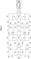
- FIG. 2 when an order of the ADC is increased so as to improve voltage measurement accuracy and reduce a measurement time, the number of amplifiers AMPs required for a configuration of a circuit is increased so that there is a problem in that an area (size) of the circuit is increased.
- Various embodiments are directed to an apparatus for measuring a voltage, which can improve accuracy and reduce a measurement time with a small area, when measuring a voltage of a battery cell or the like, by increasing an order of an analog-to-digital converter (ADC) without increasing the number of amplifiers of the ADC.
- ADC analog-to-digital converter
- an apparatus for measuring a voltage includes a primary integrator circuit configured to operate as a first integral stage of a sigma-delta analog-to-digital converter (ADC) circuit by a switching according to a control signal of a controller, a secondary integrator circuit configured to operate as a second integral stage by a switching of the controller, a comparator configured to compare final voltages modulated through the primary integrator circuit and the secondary integrator circuit, and a digital filter configured to delay an output of the comparator by a specified number of clocks according to a switching of the controller, pass the delayed output through a digital-to-analog converter (DAC) to feed the delayed output back to the primary and secondary integrator circuits, and receive the delayed output signal of the comparator as an input, wherein an output of the digital filter becomes a final measured value.
- ADC analog-to-digital converter
- the sigma-delta ADC may include an amplifier (AMP) for an integrator, the amplifier (AMP) may be used as an amplifier (AMP) for an integrator of the primary integrator circuit when the primary integrator circuit operates, and the amplifier (AMP) may be used as an amplifier (AMP) for an integrator of the secondary integrator circuit when the secondary integrator circuit operates.
- AMP amplifier
- AMP amplifier
- AMP amplifier
- the controller may output an ST signal to operate the primary integrator circuit and output an ND signal to operate the secondary integrator circuit, the primary integrator circuit may operate when the ST signal is in a high section, and the secondary integrator circuit may operate when the ND signal, which is an inverted signal of the ST signal, is in a high section so that the controller may sequentially operate the primary integrator circuit and the secondary integrator circuit.
- the primary integrator circuit may include an integrating circuit formed of a first switching capacitor part and the amplifier (AMP); the first switching capacitor part may include first, second, and third switching parts; the first switching part may include first and second switches (SW1, SW2) having first contact points commonly connected to a positive (+) terminal of a battery cell (CELL), and third and fourth switches (SW3, SW4) having first contact points commonly connected to a negative (-) terminal of the battery cell (CELL); and second contact points of the first and third switches (SW1, SW3) may be commonly connected; second contact points of the second and fourth switches (SW2, SW4) may be commonly connected; one ends of insulating capacitors (C1-1, C1-2) having the same value may be connected in series to the second contact points of the first and third switches (SW1, SW3) and to the second contact points of the second and fourth switches (SW2, SW4); and a fifth switch (SW5) and a sixth switch (SW6) may be connected in series to the other ends of the insulating capacitors (C1-1, C1-2) to be
- the first and fourth switches may be simultaneously switched on/off by an STX1 signal
- the second and third switches may be simultaneously switched on/off by an STX2 signal which is an inverted signal of the STX1 signal
- the fifth and sixth switches may be simultaneously switched on/off by the ST signal.
- the second switching part may include a seventh switch (SW7) having a first contact point which receives a second positive measured voltage (DAC2P), an eighth switch (SW8) having a first contact point which receives a reference voltage (VCM) and having a second contact point commonly connected to a second contact point of the seventh switch (SW7), an insulating capacitor (C3-1) having one end connected to the second contact point at which the seventh and eighth switches (SW7, SW8) are commonly connected, a ninth switch (SW9) having a first contact point which receives the reference voltage VCM and having a second contact point connected to the other end of the insulating capacitor (C3-1), and a tenth switch (SW10) having a first contact point commonly connected to the second contact point of the ninth switch (SW9) and the other end of the insulating capacitor (C3-1) and having a second contact point connected to the one input terminal of the amplifier (AMP), wherein the second positive measured voltage (DAC2P) may be a voltage that is feedback of a positive voltage output from DAC2P
- the seventh and ninth switches may be simultaneously switched on/off by an STQ1 signal
- the eighth and tenth switches may be simultaneously switched on/off by an STQ2 signal.
- the third switching part may include an eleventh switch (SW11) having a first contact point which receives a second negative measured voltage DAC2N, a twelfth switch (SW12) having a first contact point which receives the reference voltage (VCM) and having a second contact point commonly connected to a second contact point of the eleventh switch (SW11), an insulating capacitor (C3-2) having one end connected to the second contact point at which the eleventh and twelfth switches (SW11, SW12) are commonly connected, a thirteenth switch (SW13) having a first contact point which receives the reference voltage (VCM) and having a second contact point connected to the other end of the insulating capacitor (C3-2), and a fourteenth switch (SW14) having a first contact point commonly connected to the second contact point of the thirteenth switch (SW13) and the other end of the insulating capacitor (C3-2) and having a second contact point connected to the other input terminal of the amplifier (AMP), wherein the second negative measured voltage (DAC2N
- the eleventh and thirteenth switches may be simultaneously switched on/off by the STQ1 signal
- the twelfth and fourteenth switches may be simultaneously switched on/off by the STQ2 signal
- the STQ1 signal and the STQ2 signal may be output when the ST signal is in a high section while the primary integrator circuit operates.
- the secondary integrator circuit may include an integrating circuit formed of a second switching capacitor part and the amplifier (AMP); the second switching capacitor part may include fourth, fifth, sixth, and seventh switching parts; the fourth switching part may include a seventeenth switch (SW17) having a first contact point which receives an amplifier positive output voltage (VOUTP), an eighteenth switch (SW18) having a first contact point which receives the reference voltage (VCM) and having a second contact point commonly connected to a second contact point of the seventeenth switch (SW17), an insulating capacitor (C5-1) having one end connected to the second contact point at which the seventeenth and eighteenth switches (SW17, SW18) are commonly connected, a nineteenth switch (SW19) having a first contact point which receives the reference voltage (VCM) and having a second contact point connected to the other end of the insulating capacitor (C5-1), and a twentieth switch (SW20) having a first contact point commonly connected to the second contact point of the nineteenth switch (SW19) and the other end of
- the seventeenth and nineteenth switches may be simultaneously switched on/off by an NDQ1 signal
- the eighteenth and twentieth switches may be simultaneously switched on/off by an NDQ2 signal.
- the fifth switching part may include a twenty-first switch (SW21) having a first contact point which receives a first positive measured voltage DAC1P, a twenty-second switch (SW22) having a first contact point which receives the reference voltage (VCM) and having a second contact point commonly connected to a second contact point of the twenty-first switch (SW21), an insulating capacitor (C6-1) having one end connected to the second contact point at which the twenty-first and twenty-second switches (SW21, SW22) are commonly connected, a twenty-third switch (SW23) having a first contact point which receives the reference voltage (VCM) and having a second contact point connected to the other end of the insulating capacitor (C6-1), and a twenty-fourth switch (SW24) having a first contact point commonly connected to the second contact point of the twenty-third switch (SW23) and the other end of the insulating capacitor (C6-1) and having a second contact point connected to the one input terminal of the amplifier (AMP), wherein the first switch (SW21
- the twenty-first and twenty-third switches may be simultaneously switched on/off by the NDQ1 signal
- the twenty-second and twenty-fourth switches may be simultaneously switched on/off by the NDQ2 signal.
- the sixth switching part may include a twenty-sixth switch (SW26) having a first contact point which receives an amplifier negative output voltage (VOUTN), a twenty-seventh switch (SW27) having a first contact point which receives the reference voltage (VCM) and having a second contact point commonly connected to a second contact point of the twenty-sixth switch (SW26), an insulating capacitor (C5-2) having one end connected to the second contact point at which the twenty-sixth and twenty-seventh switches (SW26, SW27) are commonly connected, a twenty-eighth switch (SW28) having a first contact point which receives the reference voltage (VCM) and having a second contact point connected to the other end of the insulating capacitor (C5-2), and a twenty-ninth switch (SW29) having a first contact point commonly connected to the second contact point of the twenty-eighth switch (SW28) and the other end of the insulating capacitor (C5-2) and having a second contact point connected to the other input
- SW26
- the twenty-sixth and twenty-eighth switches may be simultaneously switched on/off by the NDQ1 signal
- the twenty-seventh and twenty-ninth switches (SW27, SW29) may be simultaneously switched on/off by the NDQ2 signal.
- the seventh switching part may include a thirtieth switch (SW30) having a first contact point which receives a first negative measured voltage (DAC1N), a thirty-first switch (SW31) having a first contact point which receives the reference voltage (VCM) and having a second contact point commonly connected to a second contact point of the thirtieth switch (SW30), an insulating capacitor (C6-2) having one end connected to the second contact point at which the thirtieth and thirty-first switches (SW30, SW31) are commonly connected, a thirty-second switch (SW32) having a first contact point which receives the reference voltage (VCM) and having a second contact point connected to the other end of the insulating capacitor (C6-2), and a thirty-third switch (SW33) having a first contact point commonly connected to the second contact point of the thirty-second switch (SW32) and the other end of the insulating capacitor (C6-2) and having a second contact point connected to the other input terminal of the amplifier (AMP), wherein the first negative negative measured voltage (
- the thirtieth and thirty-second switches may be simultaneously switched on/off by the NDQ1 signal
- the thirty-first and thirty-third switches may be simultaneously switched on/off by the NDQ2 signal
- the NDQ1 signal and the NDQ2 signal may be output when the ND signal is in a high section while the secondary integrator circuit operates.
- a capacitor (C2-1) and a fifteenth switch (SW15), which are connected in series, may be connected between one input terminal and one output terminal of the amplifier (AMP); a capacitor (C4-1) and a twenty-fifth switch (SW25), which are connected in series, may be connected between the one input terminal and the one output terminal; a reset switch may be connected between the one input terminal and the one output terminal; a capacitor (C2-2) and a sixteenth switch (SW16), which are connected in series, may be connected between the other input terminal and the other output terminal of the amplifier (AMP); a capacitor (C4-2) and a thirty-fourth (SW34), which are connected in series, may be connected between the other input terminal and the other output terminal; and a reset switch (RST) may be connected between the other input terminal and the other output terminal.
- the apparatus for measuring a voltage includes a voltage output circuit, wherein the voltage output circuit includes a first D flip-flop configured to receive one output and the other output of the comparator, a second D flip-flop connected to one output terminal and the other output terminal of the first D flip-flop, and a digital filter configured to filter and output voltages output from one output terminal and the other output terminal of the second D flip-flop, a first DAC (DAC1) is connected parallel to the one output terminal and the other output terminal of the first D flip-flop to feed a first positive measured voltage (DAC1P) and a first negative measured voltage (DAC1N) back to the secondary integrator circuit, and a second DAC (DAC2) is connected parallel to the one output terminal and the other output terminal of the second D flip-flop to feed a second positive measured voltage (DAC2P) and a second negative measured voltage (DAC2N) back to the primary integrator circuit.
- DAC1P positive measured voltage
- DAC1N first negative measured voltage
- DAC2P second positive measured voltage
- the components described in the example embodiments may be implemented by hardware components including, for example, at least one digital signal processor (DSP), a processor, a controller, an application-specific integrated circuit (ASIC), a programmable logic element, such as an FPGA, other electronic devices, or combinations thereof.
- DSP digital signal processor
- ASIC application-specific integrated circuit
- FPGA field-programmable gate array
- At least some of the functions or the processes described in the example embodiments may be implemented by software, and the software may be recorded on a recording medium.
- the components, the functions, and the processes described in the example embodiments may be implemented by a combination of hardware and software.
- the method according to example embodiments may be embodied as a program that is executable by a computer, and may be implemented as various recording media such as a magnetic storage medium, an optical reading medium, and a digital storage medium.
- Various techniques described herein may be implemented as digital electronic circuitry, or as computer hardware, firmware, software, or combinations thereof.
- the techniques may be implemented as a computer program product, i.e., a computer program tangibly embodied in an information carrier, e.g., in a machine-readable storage device (for example, a computer-readable medium) or in a propagated signal for processing by, or to control an operation of a data processing apparatus, e.g., a programmable processor, a computer, or multiple computers.
- a computer program(s) may be written in any form of a programming language, including compiled or interpreted languages and may be deployed in any form including a stand-alone program or a module, a component, a subroutine, or other units suitable for use in a computing environment.
- a computer program may be deployed to be executed on one computer or on multiple computers at one site or distributed across multiple sites and interconnected by a communication network.
- processors suitable for execution of a computer program include, by way of example, both general and special purpose microprocessors, and any one or more processors of any kind of digital computer.
- a processor will receive instructions and data from a read-only memory or a random access memory or both.
- Elements of a computer may include at least one processor to execute instructions and one or more memory devices to store instructions and data.
- a computer will also include or be coupled to receive data from, transfer data to, or perform both on one or more mass storage devices to store data, e.g., magnetic, magneto-optical disks, or optical disks.
- Examples of information carriers suitable for embodying computer program instructions and data include semiconductor memory devices, for example, magnetic media such as a hard disk, a floppy disk, and a magnetic tape, optical media such as a compact disk read only memory (CD-ROM), a digital video disk (DVD), etc. and magneto-optical media such as a floptical disk, and a read only memory (ROM), a random access memory (RAM), a flash memory, an erasable programmable ROM (EPROM), and an electrically erasable programmable ROM (EEPROM) and any other known computer readable medium.
- a processor and a memory may be supplemented by, or integrated into, a special purpose logic circuit.
- the processor may run an operating system (OS) and one or more software applications that run on the OS.
- the processor device also may access, store, manipulate, process, and create data in response to execution of the software.
- OS operating system
- the description of a processor device is used as singular; however, one skilled in the art will be appreciated that a processor device may include multiple processing elements and/or multiple types of processing elements.
- a processor device may include multiple processors or a processor and a controller.
- different processing configurations are possible, such as parallel processors.
- non-transitory computer-readable media may be any available media that may be accessed by a computer, and may include both computer storage media and transmission media.
- components that are distinguished from each other are intended to clearly illustrate each feature. However, it does not necessarily mean that the components are separate. That is, a plurality of components may be integrated into one hardware or software unit, or a single component may be distributed into a plurality of hardware or software units. Thus, unless otherwise noted, such integrated or distributed embodiments are also included within the scope of the present disclosure.
- components described in the various embodiments are not necessarily essential components, and some may be optional components. Accordingly, embodiments consisting of a subset of the components described in one embodiment are also included within the scope of the present disclosure. In addition, embodiments that include other components in addition to the components described in the various embodiments are also included in the scope of the present disclosure.
- a component when referred to as being "linked,” “coupled,” or “connected” to another component, it is understood that not only a direct connection relationship but also an indirect connection relationship through an intermediate component may also be included.
- a component when referred to as “comprising” or “having” another component, it may mean further inclusion of another component not the exclusion thereof, unless explicitly described to the contrary.
- first, second, etc. are used only for the purpose of distinguishing one component from another, and do not limit the order or importance of components, etc., unless specifically stated otherwise.
- a first component in one exemplary embodiment may be referred to as a second component in another embodiment, and similarly a second component in one exemplary embodiment may be referred to as a first component.
- components that are distinguished from each other are intended to clearly illustrate each feature. However, it does not necessarily mean that the components are separate. That is, a plurality of components may be integrated into one hardware or software unit, or a single component may be distributed into a plurality of hardware or software units. Thus, unless otherwise noted, such integrated or distributed embodiments are also included within the scope of the present disclosure.
- components described in the various embodiments are not necessarily essential components, and some may be optional components. Accordingly, embodiments consisting of a subset of the components described in one embodiment are also included within the scope of the present disclosure. In addition, exemplary embodiments that include other components in addition to the components described in the various embodiments are also included in the scope of the present disclosure.
- FIG. 3 is an exemplary diagram illustrating a circuit configuration of an apparatus for measuring a voltage according to one embodiment of the present disclosure
- FIG. 4 is an exemplary diagram illustrating a timing chart of control signals output from a controller to switches of the apparatus for measuring a voltage shown in FIG. 3 .
- the apparatus for measuring a voltage includes a primary integrator circuit 110 configured to operate as a first integral stage of a sigma-delta analog-to-digital converter (ADC) circuit by a switching according to a control signal of a controller 150, secondary integrator circuits 120 and 130 configured to operate as a second integrator stage by the switching of the controller 150, and a voltage output circuit 140 configured to delay an output of the primary integrator circuit 110 by a specified number of clocks according to the switching of the controller 150 to feed the delayed output back to the secondary integrator circuits 120 and 130, delay outputs of the secondary integrator circuits 120 and 130 by a specified number of clocks to feed the delayed outputs back to the primary integrator circuit 110, and output a finally measured voltage value through the primary integrator circuit 110 and the secondary integrator circuits 120 and 130.
- ADC analog-to-digital converter
- an amplifier AMP is used as an amplifier AMP for an integrator of the primary integrator circuit 110 and, when the secondary integrator circuit 120 operates, the AMP is used as an amplifier AMP for an integrator of the secondary integrator circuit 120.
- the primary integrator circuit 110 when an ST signal is in a high section, the primary integrator circuit 110 operates (for convenience, it is indicated by a thick line), and when an ND signal is in a high section, the secondary integrator circuit 120 operates. In this case, since the ST signal and the ND signal are inverted pulse signals, the primary integrator circuit 110 and the secondary integrator circuit 120 operate sequentially.
- the present embodiment is characterized in that a circuit in which the primary integrator circuit 110 and the secondary integrator circuit 120 operate sequentially is configured so that a single amplifier AMP is actually used to achieve the same effect as a circuit in which two amplifiers AMP are used as shown in FIG. 2 to increase an order of ADC (e.g., a sigma-delta ADC circuit).
- a circuit in which the primary integrator circuit 110 and the secondary integrator circuit 120 operate sequentially is configured so that a single amplifier AMP is actually used to achieve the same effect as a circuit in which two amplifiers AMP are used as shown in FIG. 2 to increase an order of ADC (e.g., a sigma-delta ADC circuit).
- the primary integrator circuit 110 includes an integrating circuit formed of a first switching capacitor part (i.e., first to third switching parts 111 to 113 and capacitors C2-1 and C2-2) and the amplifier AMP, and the secondary integrator circuits 120 and 130 include an integrating circuit formed of a second switching capacitor part (i.e., fourth to seventh switching parts 121, 122, 131, and 132, capacitors C4-1 and C4-2), and the amplifier AMP.
- a first switching capacitor part i.e., first to third switching parts 111 to 113 and capacitors C2-1 and C2-2
- the secondary integrator circuits 120 and 130 include an integrating circuit formed of a second switching capacitor part (i.e., fourth to seventh switching parts 121, 122, 131, and 132, capacitors C4-1 and C4-2), and the amplifier AMP.
- the first switching part 111 includes first and second switches SW1 and SW2 each having a first contact point commonly connected to a positive (+) terminal of a battery cell CELL, and third and fourth switches SW3 and SW4 each having a first contact point commonly connected to a negative (-) terminal of the battery cell CELL. Second contact points of the first and third switches SW1 and SW3 are commonly connected, and second contact points of the second and fourth switches SW2 and SW4 are commonly connected. In addition, one ends of insulating capacitors C1-1 and C1-2 having the same value are connected in series to the second contact points of the first and third switches SW1 and SW3 and the second contact points of the second and fourth switches SW2 and SW4.
- a fifth switch SW5 and a sixth switch SW6 are connected in series to the other ends of the insulating capacitors C1-1 and C1-2 to be connected to one input terminal (e.g., a non-inverting input terminal) and the other input terminal (e.g., an inverting input terminal) of the amplifier AMP.
- the first and fourth switches SW1 and SW4 are simultaneously switched on/off by an STX1 signal (that is, switched on in a high section and switched off in a low section), the second and third switches SW2 and SW3 are simultaneously switched on/off by an STX2 signal, and the fifth and sixth switches SW5 and SW6 are simultaneously switched on/off by the ST signal.
- an STX1 signal that is, switched on in a high section and switched off in a low section
- the second and third switches SW2 and SW3 are simultaneously switched on/off by an STX2 signal
- the fifth and sixth switches SW5 and SW6 are simultaneously switched on/off by the ST signal.
- the second switching part 112 includes a seventh switch SW7 having a first contact point which receives a second positive measured voltage DAC2P (i.e., a voltage which is feedback of a positive voltage output from a second DAC DAC2 146 after the ST signal is delayed by two clocks through a second D flip-flop 145), an eighth switch SW8 having a first contact point which receives a reference voltage VCM and having a second contact point commonly connected to a second contact point of the seventh switch SW7, an insulating capacitor C3-1 having one end connected to the second contact point at which the seventh and eighth switches SW7 and SW8 are commonly connected, a ninth switch SW9 having a first contact point which receives the reference voltage VCM and having a second contact point connected to the other end of the insulating capacitor C3-1, and a tenth switch SW10 having a first contact point commonly connected to the second contact point of the ninth switch SW9 and the other end of the insulating capacitor C3-1 and having a second contact point connected to the one input terminal (
- the seventh and ninth switches SW7 and SW9 are simultaneously switched on/off by an STQ1 signal (i.e., switched on in a high section and switched off in a low section), and the eighth and tenth switches SW8 and SW10 are simultaneously switched on/off by an STQ2 signal.
- the third switching part 113 includes an eleventh switch SW11 having a first contact point which receives a second negative measured voltage DAC2N (i.e., a voltage which is feedback of a negative voltage output from the second DAC DAC2 146 after the ST signal is delayed by two clocks through the second D flip-flop 145), a twelfth switch SW12 having a first contact point which receives the reference voltage VCM and having a second contact point commonly connected to a second contact point of the eleventh switch SW11, an insulating capacitor C3-2 having one end connected to the second contact point at which the eleventh and twelfth switches SW11 and SW12 are commonly connected, a thirteenth switch SW13 having a first contact point which receives the reference voltage VCM and having a second contact point connected to the other end of the insulating capacitor C3-2, and a fourteenth switch SW14 having a first contact point commonly connected to the second contact point of the thirteenth switch SW13 and the other end of the insulating capacitor C3-2 and having a second contact point connected
- the eleventh and thirteenth switches SW11 and SW13 are simultaneously switched on/off by the STQ1 signal (i.e., switched on in a high section and switched off in a low section), and the twelfth and fourteenth switches SW12 and SW14 are simultaneously switched on/off by the STQ2 signal.
- the STQ1 signal and the STQ2 signal are output when the primary integrator circuit 110 operates (i.e., when the ST signal is in the high section).
- the fourth switching part 121 includes a seventeenth switch SW17 having a first contact point which receives an amplifier positive output voltage VOUTP (i.e., a voltage which is feedback of a positive voltage output from the amplifier AMP), an eighteenth switch SW18 having a first contact point which receives the reference voltage VCM and having a second contact point commonly connected to a second contact point of the seventeenth switch SW17, an insulating capacitor C5-1 having one end connected to the second contact point at which the seventeenth and eighteenth switches SW17 and SW18 are commonly connected, a nineteenth switch SW19 having a first contact point which receives the reference voltage VCM and having a second contact point connected to the other end of the insulating capacitor C5-1, and a twentieth switch SW20 having a first contact point commonly connected to the second contact point of the nineteenth switch SW19 and the other end of the insulating capacitor C5-1 and having a second contact point connected to the one input terminal (e.g., the non-inverting input terminal) of the amplifier AMP.
- the seventeenth and nineteenth switches SW17 and SW19 are simultaneously switched on/off by an NDQ1 signal (i.e., switched on in a high section and switched off in a low section), and the eighteenth and twentieth switches SW18 and SW20 are simultaneously switched on/off by an NDQ2 signal.
- the fifth switching part 122 includes a twenty-first switch SW21 having a first contact point which receives a first positive measured voltage DAC1P (i.e., a voltage which is feedback of a positive voltage output from a first DAC DAC1 144 after the ST signal is delayed by one clock through a first D flip-flop 143, a twenty-second switch SW22 having a first contact point which receives the reference voltage VCM and having a second contact point commonly connected to a second contact point of the twenty-first switch SW21, an insulating capacitor C6-1 having one end connected to the second contact point at which the twenty-first and twenty-second switches SW21 and SW22 are commonly connected, a twenty-third switch SW23 having a first contact point which receives the reference voltage VCM and having a second contact point connected to the other end of the insulating capacitor C6-1, and a twenty-fourth switch SW24 having a first contact point commonly connected to the second contact point of the twenty-third switch SW23 and the other end of the insulating capacitor C6-1
- the twenty-first and twenty-third switches SW21 and SW23 are simultaneously switched on/off by the NDQ1 signal (i.e., switched on in the high section and switched off in the low section), and the twenty-second and twenty-fourth switches SW22 and SW24 are simultaneously switched on/off by the NDQ2 signal.
- the sixth switching part 131 includes a twenty-sixth switch SW26 having a first contact point which receives an amplifier negative output voltage VOUTN (i.e., a voltage which is feedback of a negative voltage output from the amplifier AMP), a twenty-seventh switch SW27 having a first contact point which receives the reference voltage VCM and having a second contact point commonly connected to a second contact point of the twenty-sixth switch SW26, an insulating capacitor C5-2 having one end connected to the second contact point at which the twenty-sixth and twenty-seventh switches SW26 and SW27 are commonly connected, a twenty-eighth switch SW28 having a first contact point which receives the reference voltage VCM and having a second contact point connected to the other end of the insulating capacitor C5-2, and a twenty-ninth switch SW29 having a first contact point commonly connected to the second contact point of the twenty-eighth switch SW28 and the other end of the insulating capacitor C5-2 and having a second contact point connected to the other input terminal (e
- the twenty-sixth and twenty-eighth switches SW26 and SW28 are simultaneously switched on/off by the NDQ1 signal (i.e., switched on in the high section and switched off in the low section), and the twenty-seventh and twenty-ninth switches SW27 and SW29 are simultaneously switched on/off by the NDQ2 signal.
- the seventh switching part 132 includes a thirtieth switch SW30 having a first contact point which receives a first negative measured voltage DAC1N (i.e., a voltage which is feedback of a negative voltage output from the first DAC DAC1 144 after the ST signal is delayed by one clock through the first D flip-flop 143, a thirty-first switch SW31 having a first contact point which receives the reference voltage VCM and having a second contact point commonly connected to a second contact point of the thirtieth switch SW30, an insulating capacitor C6-2 having one end connected to the second contact point at which the thirtieth and thirty-first switches SW30 and SW31 are commonly connected, a thirty-second switch SW32 having a first contact point which receives the reference voltage VCM and having a second contact point connected to the other end of the insulating capacitor C6-2, and a thirty-third switch SW33 having a first contact point commonly connected to the second contact point of the thirty-second switch SW32 and the other end of the insulating capacitor C6-2 and having
- the thirtieth and thirty-second switches SW30 and SW32 are simultaneously switched on/off by the NDQ1 signal (i.e., switched on in the high section and switched off in the low section), and the thirty-first and thirty-third switches SW31 and SW33 are simultaneously switched on/off by the NDQ2 signal.
- the NDQ1 signal and the NDQ2 signal are output when the secondary integrator circuits 120 and 130 operate (i.e., when the ND signal is in the high section).
- the capacitor C2-1 and a fifteenth switch SW15 which are connected in series, are connected between the one input terminal (e.g., the non-inverting input terminal) and one output terminal (e.g., a VOUTP output terminal) of the amplifier AMP
- the capacitor C4-1 and a fifteenth switch SW25 which are connected in series, are also connected between the one input terminal (e.g., the non-inverting input terminal) and the one output terminal (e.g., the VOUTP output terminal) of the amplifier AMP
- a reset switch RST is additionally connected between the one input terminal (e.g., the non-inverting input terminal) and the one output terminal (e.g., the VOUTP output terminal) of the amplifier AMP.
- the capacitor C2-2 and a sixteenth switch SW16 which are connected in series, are connected between the other input terminal (e.g., the inverting input terminal) and the other output terminal (e.g., the VOUTN output terminal) of the amplifier AMP
- the capacitor C4-2 and a thirty-fourth switch SW34 which are connected in series, are also connected between the other input terminal (e.g., the inverting input terminal) and the other output terminal (e.g., the VOUTN output terminal) of the amplifier AMP
- a reset switch RST is additionally connected between the other input terminal (e.g., the inverting input terminal) and the other output terminal (e.g., the VOUTN output terminal) of the amplifier AMP.
- the primary integrator circuit 110 when the ST signal is in the high section, the primary integrator circuit 110 operates, and thus the fifteenth and sixteenth switches SW15 and SW16 are switched on so that the amplifier AMP and the two capacitors C2-1 and C2-2 operate as an integrator.
- the secondary integrator circuits 120 and 130 when the ND signal is in the high section, the secondary integrator circuits 120 and 130 operate, and thus the twenty-fifth and thirty-fourth switches SW25 and SW34 are switched on so that the amplifier AMP and the two capacitors C4-1 and C4-2 operate as an integrator.
- the voltage output circuit 140 includes a comparator 141 connected to the one output terminal and the other output terminal of the amplifier AMP and configured to compare magnitudes of outputs (i.e., a finally modulated voltage through the primary integrator circuit and the secondary integrator circuits), an SR-latch 142 connected to one output terminal and the other output terminal of the comparator 141, the first D flip-flop 143 connected to one output terminal and the other output terminal of the SR-latch 142, the second D flip-flop 145 connected to one output terminal and the other output terminal of the first D flip-flop 143, and a digital filter 147 configured to filter and output voltages DOUT and DOUTB output from one output terminal and the other output terminal of the second D flip-flop 145.
- a comparator 141 connected to the one output terminal and the other output terminal of the amplifier AMP and configured to compare magnitudes of outputs (i.e., a finally modulated voltage through the primary integrator circuit and the secondary integrator circuits)
- an SR-latch 142 connected
- the digital filter 147 delays the output of the comparator 141 by a specified number of clocks according to the switching of the controller 150, passes the delayed output through the DAC to feed the delayed output back to the primary integrator circuit 110 and the secondary integrator circuits 120 and 130, and receives the delayed output signal of the comparator 141.
- first DAC DAC1 144 is connected parallel to the one output terminal and the other output terminal of the first D flip-flop 143 to feed the first positive measured voltage DAC1P and the first negative measured voltage DAC1N back to the secondary integrator circuits 120 and 130
- second DAC DAC2 146 is connected parallel to the one output terminal and the other output terminal of the second D flip-flop 145 to feed the second positive measured voltage DAC2P and the second negative measured voltage DAC2N back to the primary integrator circuit 110.
- the first D flip-flop 143 and the second D flip-flop 145 each receive the ST signal as a clock. That is, the first D flip-flop 143 feeds a value, which is output from the amplifier AMP and delayed by one clock by the ST signal, back to the secondary integrator circuits 120 and 130, and the second D flip-flop 145 feeds a value, which is output from the amplifier AMP and delayed by two clocks by the ST signal, back to the primary integrator circuit 110.
- the apparatus for measuring a voltage is configured such that the values obtained by delaying two clocks and one clock using the first and second D flip-flops 143 and 145 undergo DA conversion through the first DAC DAC1 144 and the second DAC DAC2 146 and are then fed back.
- the primary integrator circuit 110 and the secondary integrator circuits 120 and 130 actually use a single amplifier AMP, they operate, as shown in FIG. 2 , in the same way as a circuit (e.g., a sigma-delta ADC circuit) in which the order of the ADC is increased using two amplifiers AMP.
- a circuit e.g., a sigma-delta ADC circuit
- the present embodiment while relatively further reducing the size of the circuit, there is an effect of increasing the voltage measurement speed to reduce the voltage measurement time and also to improve the voltage measurement accuracy.
- FIG. 4 is an exemplary diagram illustrating a timing chart of control signals output from a controller to switches of the apparatus for measuring a voltage shown in FIG. 3 .
- the controller 150 outputs the ST signal in a high state
- the fifth, sixth, fifteenth, and sixteenth switches SW5, SW6, SW15, and SW16 of the primary integrator circuit 110 are switched on
- the primary integrator circuit 110 performs sampling in the high sections of the STX1 signal and the STQ1 signal (e.g., a former half high section of the ST signal)
- the primary integrator circuit 110 performs an integral calculation (i.e., an integral calculation on a value fed back through the second D flip-flop 145 and the second DAC DAC2 146) in the high sections of the STX2 signal and the STQ2 signal (e.g., a latter half high section of the ST signal).
- a value (that is, a measured voltage value) output after the integral calculation is completed by the primary integrator circuit 110 is fed back to the secondary integrator circuits 120 and 130 through the first D flip-flop 143 and the first DAC DAC1 144.
- the twenty-fifth and thirty-fourth switches SW25 and SW34 of the secondary integrator circuits 120 and 130 are switched on, the secondary integrator circuits 120 and 130 perform sampling in the high section of the NDQ1 signal (e.g., a former half high period of the ND signal), and the secondary integrator circuits 120 and 130 perform an integral calculation (i.e., an integral calculation on a difference between a value fed back through the first D flip-flop 143 and the first DAC DAC1 144 and the value output from the amplifier) in the high section of the NDQ2 signal (e.g., a latter half high section of the ND signal).
- an integral calculation i.e., an integral calculation on a difference between a value fed back through the first D flip-flop 143 and the first DAC DAC1 144 and the value output from the amplifier
- the controller 150 sequentially operates the primary integrator circuit 110 and the secondary integrator circuits 120 and 130 according to a switch control signal in the form of a pulse that is periodically output, so that, while the primary integrator circuit 110 and the secondary integrator circuits 120 and 130 actually use a single amplifier AMP, they operate, as shown in FIG. 2 , in the same way as a circuit (e.g., a sigma-delta ADC circuit) in which the order of the ADC is increased using two amplifiers AMP. Rather, according to the present embodiment, while relatively further reducing the size of the circuit, there is an effect of increasing the voltage measurement speed to reduce the voltage measurement time and also to improve the voltage measurement accuracy.
- a circuit e.g., a sigma-delta ADC circuit
Landscapes
- Physics & Mathematics (AREA)
- General Physics & Mathematics (AREA)
- Engineering & Computer Science (AREA)
- Theoretical Computer Science (AREA)
- Power Engineering (AREA)
- Mathematical Physics (AREA)
- Manufacturing & Machinery (AREA)
- Chemical & Material Sciences (AREA)
- Chemical Kinetics & Catalysis (AREA)
- Electrochemistry (AREA)
- General Chemical & Material Sciences (AREA)
- Analogue/Digital Conversion (AREA)
- Measurement Of Current Or Voltage (AREA)
Abstract
Description
- Exemplary embodiments of the present disclosure relate to an apparatus for measuring a voltage, and more particularly, to an apparatus for measuring a voltage, which can improve accuracy and reduce a measurement time with a small area, when measuring a voltage of a battery cell or the like, by increasing an order of an analog-to-digital converter (ADC) without increasing the number of amplifiers of the ADC.
- Generally, in electric vehicles (EVs) and hybrid EVs (HEVs), electric motors are driven by using batteries (or fuel cells).
- Therefore, voltage measurement (or voltage monitoring) of each cell of a battery (or fuel cell) is required for voltage control (e.g., voltage balancing control for minimizing a voltage difference between cells).
- A voltage measurement circuit used in this case generally employs a method of selecting one of a number of battery cells using a multiplexer (MUX), converting a high voltage into a low voltage, and then detecting the low voltage as a digital value using an analog-to-digital converter (ADC). In this case, as described above, since a high voltage element is generally used in order to convert the high voltage into the low voltage, the size of the voltage measurement circuit increases. Therefore, the MUX is used, but a switching element constituting the MUX should also be formed as the high voltage element. Accordingly, there are problems in that the overall size and costs of the apparatus for measuring a voltage increase and a cell voltage sensing speed is limited.
- Accordingly, as shown in
FIG. 1 , the inventor of the present disclosure has developed a voltage measurement circuit using a primary ADC enabling the use of a low voltage element instead of a high voltage element by integrating a high voltage processing function with an ADC function. However, as shown inFIG. 2 , when an order of the ADC is increased so as to improve voltage measurement accuracy and reduce a measurement time, the number of amplifiers AMPs required for a configuration of a circuit is increased so that there is a problem in that an area (size) of the circuit is increased. - Therefore, there is a need for an apparatus for measuring a voltage, which has an effect of increasing the order of the ADC without increasing the number of amplifier AMPs and thus can relatively reduce the size of the circuit compared to the case of increasing the number of amplifier AMPs, increase an operating speed of the circuit to increase a voltage measurement speed, and improve voltage measurement accuracy.
- The background art of the present disclosure is disclosed in
Korean Patent Registration No. 10-1527136 (registered on June 2, 2015 - Various embodiments are directed to an apparatus for measuring a voltage, which can improve accuracy and reduce a measurement time with a small area, when measuring a voltage of a battery cell or the like, by increasing an order of an analog-to-digital converter (ADC) without increasing the number of amplifiers of the ADC.
- In an embodiment, an apparatus for measuring a voltage includes a primary integrator circuit configured to operate as a first integral stage of a sigma-delta analog-to-digital converter (ADC) circuit by a switching according to a control signal of a controller, a secondary integrator circuit configured to operate as a second integral stage by a switching of the controller, a comparator configured to compare final voltages modulated through the primary integrator circuit and the secondary integrator circuit, and a digital filter configured to delay an output of the comparator by a specified number of clocks according to a switching of the controller, pass the delayed output through a digital-to-analog converter (DAC) to feed the delayed output back to the primary and secondary integrator circuits, and receive the delayed output signal of the comparator as an input, wherein an output of the digital filter becomes a final measured value.
- In the present disclosure, the sigma-delta ADC may include an amplifier (AMP) for an integrator, the amplifier (AMP) may be used as an amplifier (AMP) for an integrator of the primary integrator circuit when the primary integrator circuit operates, and the amplifier (AMP) may be used as an amplifier (AMP) for an integrator of the secondary integrator circuit when the secondary integrator circuit operates.
- In the present disclosure, the controller may output an ST signal to operate the primary integrator circuit and output an ND signal to operate the secondary integrator circuit, the primary integrator circuit may operate when the ST signal is in a high section, and the secondary integrator circuit may operate when the ND signal, which is an inverted signal of the ST signal, is in a high section so that the controller may sequentially operate the primary integrator circuit and the secondary integrator circuit.
- In the present disclosure, the primary integrator circuit may include an integrating circuit formed of a first switching capacitor part and the amplifier (AMP); the first switching capacitor part may include first, second, and third switching parts; the first switching part may include first and second switches (SW1, SW2) having first contact points commonly connected to a positive (+) terminal of a battery cell (CELL), and third and fourth switches (SW3, SW4) having first contact points commonly connected to a negative (-) terminal of the battery cell (CELL); and second contact points of the first and third switches (SW1, SW3) may be commonly connected; second contact points of the second and fourth switches (SW2, SW4) may be commonly connected; one ends of insulating capacitors (C1-1, C1-2) having the same value may be connected in series to the second contact points of the first and third switches (SW1, SW3) and to the second contact points of the second and fourth switches (SW2, SW4); and a fifth switch (SW5) and a sixth switch (SW6) may be connected in series to the other ends of the insulating capacitors (C1-1, C1-2) to be connected to one input terminal and the other input terminal of the amplifier (AMP).
- In the present disclosure, the first and fourth switches (SW1, SW4) may be simultaneously switched on/off by an STX1 signal, the second and third switches (SW2, SW3) may be simultaneously switched on/off by an STX2 signal which is an inverted signal of the STX1 signal, and the fifth and sixth switches (SW5, SW6) may be simultaneously switched on/off by the ST signal.
- In the present disclosure, the second switching part may include a seventh switch (SW7) having a first contact point which receives a second positive measured voltage (DAC2P), an eighth switch (SW8) having a first contact point which receives a reference voltage (VCM) and having a second contact point commonly connected to a second contact point of the seventh switch (SW7), an insulating capacitor (C3-1) having one end connected to the second contact point at which the seventh and eighth switches (SW7, SW8) are commonly connected, a ninth switch (SW9) having a first contact point which receives the reference voltage VCM and having a second contact point connected to the other end of the insulating capacitor (C3-1), and a tenth switch (SW10) having a first contact point commonly connected to the second contact point of the ninth switch (SW9) and the other end of the insulating capacitor (C3-1) and having a second contact point connected to the one input terminal of the amplifier (AMP), wherein the second positive measured voltage (DAC2P) may be a voltage that is feedback of a positive voltage output from a second DAC (DAC2) after the ST signal is delayed by two clocks through a second D flip-flop of a voltage output circuit.
- In the present disclosure, the seventh and ninth switches (SW7, SW9) may be simultaneously switched on/off by an STQ1 signal, and the eighth and tenth switches (SW8, SW10) may be simultaneously switched on/off by an STQ2 signal.
- In the present disclosure, the third switching part may include an eleventh switch (SW11) having a first contact point which receives a second negative measured voltage DAC2N, a twelfth switch (SW12) having a first contact point which receives the reference voltage (VCM) and having a second contact point commonly connected to a second contact point of the eleventh switch (SW11), an insulating capacitor (C3-2) having one end connected to the second contact point at which the eleventh and twelfth switches (SW11, SW12) are commonly connected, a thirteenth switch (SW13) having a first contact point which receives the reference voltage (VCM) and having a second contact point connected to the other end of the insulating capacitor (C3-2), and a fourteenth switch (SW14) having a first contact point commonly connected to the second contact point of the thirteenth switch (SW13) and the other end of the insulating capacitor (C3-2) and having a second contact point connected to the other input terminal of the amplifier (AMP), wherein the second negative measured voltage (DAC2N) may be a voltage that is feedback of a negative voltage output from the second DAC (DAC2) after the ST signal is delayed by two clocks through the second D flip-flop of the voltage output circuit.
- In the present disclosure, the eleventh and thirteenth switches (SW11, SW13) may be simultaneously switched on/off by the STQ1 signal, the twelfth and fourteenth switches (SW12, SW14) may be simultaneously switched on/off by the STQ2 signal, and the STQ1 signal and the STQ2 signal may be output when the ST signal is in a high section while the primary integrator circuit operates.
- In the present disclosure, the secondary integrator circuit may include an integrating circuit formed of a second switching capacitor part and the amplifier (AMP); the second switching capacitor part may include fourth, fifth, sixth, and seventh switching parts; the fourth switching part may include a seventeenth switch (SW17) having a first contact point which receives an amplifier positive output voltage (VOUTP), an eighteenth switch (SW18) having a first contact point which receives the reference voltage (VCM) and having a second contact point commonly connected to a second contact point of the seventeenth switch (SW17), an insulating capacitor (C5-1) having one end connected to the second contact point at which the seventeenth and eighteenth switches (SW17, SW18) are commonly connected, a nineteenth switch (SW19) having a first contact point which receives the reference voltage (VCM) and having a second contact point connected to the other end of the insulating capacitor (C5-1), and a twentieth switch (SW20) having a first contact point commonly connected to the second contact point of the nineteenth switch (SW19) and the other end of the insulating capacitor (C5-1) and having a second contact point connected to the one input terminal of the amplifier (AMP), and the amplifier positive output voltage (VOUTP) may be a voltage that is feedback of a positive voltage output from the amplifier (AMP).
- In the present disclosure, the seventeenth and nineteenth switches (SW17, SW19) may be simultaneously switched on/off by an NDQ1 signal, and the eighteenth and twentieth switches (SW18, SW20) may be simultaneously switched on/off by an NDQ2 signal.
- In the present disclosure, the fifth switching part may include a twenty-first switch (SW21) having a first contact point which receives a first positive measured voltage DAC1P, a twenty-second switch (SW22) having a first contact point which receives the reference voltage (VCM) and having a second contact point commonly connected to a second contact point of the twenty-first switch (SW21), an insulating capacitor (C6-1) having one end connected to the second contact point at which the twenty-first and twenty-second switches (SW21, SW22) are commonly connected, a twenty-third switch (SW23) having a first contact point which receives the reference voltage (VCM) and having a second contact point connected to the other end of the insulating capacitor (C6-1), and a twenty-fourth switch (SW24) having a first contact point commonly connected to the second contact point of the twenty-third switch (SW23) and the other end of the insulating capacitor (C6-1) and having a second contact point connected to the one input terminal of the amplifier (AMP), wherein the first positive measured voltage (DAC1P) may be a voltage that is feedback of a positive voltage output from a first DAC (DAC1) after the ST signal is delayed by one clock through a first D flip-flop of the voltage output circuit.
- In the present disclosure, the twenty-first and twenty-third switches (SW21, SW23) may be simultaneously switched on/off by the NDQ1 signal, and the twenty-second and twenty-fourth switches (SW22, SW24) may be simultaneously switched on/off by the NDQ2 signal.
- In the present disclosure, the sixth switching part may include a twenty-sixth switch (SW26) having a first contact point which receives an amplifier negative output voltage (VOUTN), a twenty-seventh switch (SW27) having a first contact point which receives the reference voltage (VCM) and having a second contact point commonly connected to a second contact point of the twenty-sixth switch (SW26), an insulating capacitor (C5-2) having one end connected to the second contact point at which the twenty-sixth and twenty-seventh switches (SW26, SW27) are commonly connected, a twenty-eighth switch (SW28) having a first contact point which receives the reference voltage (VCM) and having a second contact point connected to the other end of the insulating capacitor (C5-2), and a twenty-ninth switch (SW29) having a first contact point commonly connected to the second contact point of the twenty-eighth switch (SW28) and the other end of the insulating capacitor (C5-2) and having a second contact point connected to the other input terminal of the amplifier (AMP), wherein the amplifier negative output voltage (VOUTN) may be a voltage that is feedback of a negative voltage output from the amplifier (AMP).
- In the present disclosure, the twenty-sixth and twenty-eighth switches (SW26, SW28) may be simultaneously switched on/off by the NDQ1 signal, and the twenty-seventh and twenty-ninth switches (SW27, SW29) may be simultaneously switched on/off by the NDQ2 signal.
- In the present disclosure, the seventh switching part may include a thirtieth switch (SW30) having a first contact point which receives a first negative measured voltage (DAC1N), a thirty-first switch (SW31) having a first contact point which receives the reference voltage (VCM) and having a second contact point commonly connected to a second contact point of the thirtieth switch (SW30), an insulating capacitor (C6-2) having one end connected to the second contact point at which the thirtieth and thirty-first switches (SW30, SW31) are commonly connected, a thirty-second switch (SW32) having a first contact point which receives the reference voltage (VCM) and having a second contact point connected to the other end of the insulating capacitor (C6-2), and a thirty-third switch (SW33) having a first contact point commonly connected to the second contact point of the thirty-second switch (SW32) and the other end of the insulating capacitor (C6-2) and having a second contact point connected to the other input terminal of the amplifier (AMP), wherein the first negative measured voltage (DAC1N) may be a voltage that is feedback of a negative voltage output from the first DAC (DAC1) after the ST signal is delayed by one clock through the first D flip-flop of the voltage output circuit.
- In the present disclosure, the thirtieth and thirty-second switches (SW30, SW32) may be simultaneously switched on/off by the NDQ1 signal, the thirty-first and thirty-third switches (SW31, SW33) may be simultaneously switched on/off by the NDQ2 signal, and the NDQ1 signal and the NDQ2 signal may be output when the ND signal is in a high section while the secondary integrator circuit operates.
- In the present disclosure, a capacitor (C2-1) and a fifteenth switch (SW15), which are connected in series, may be connected between one input terminal and one output terminal of the amplifier (AMP); a capacitor (C4-1) and a twenty-fifth switch (SW25), which are connected in series, may be connected between the one input terminal and the one output terminal; a reset switch may be connected between the one input terminal and the one output terminal; a capacitor (C2-2) and a sixteenth switch (SW16), which are connected in series, may be connected between the other input terminal and the other output terminal of the amplifier (AMP); a capacitor (C4-2) and a thirty-fourth (SW34), which are connected in series, may be connected between the other input terminal and the other output terminal; and a reset switch (RST) may be connected between the other input terminal and the other output terminal.
- In the present disclosure, the apparatus for measuring a voltage includes a voltage output circuit, wherein the voltage output circuit includes a first D flip-flop configured to receive one output and the other output of the comparator, a second D flip-flop connected to one output terminal and the other output terminal of the first D flip-flop, and a digital filter configured to filter and output voltages output from one output terminal and the other output terminal of the second D flip-flop, a first DAC (DAC1) is connected parallel to the one output terminal and the other output terminal of the first D flip-flop to feed a first positive measured voltage (DAC1P) and a first negative measured voltage (DAC1N) back to the secondary integrator circuit, and a second DAC (DAC2) is connected parallel to the one output terminal and the other output terminal of the second D flip-flop to feed a second positive measured voltage (DAC2P) and a second negative measured voltage (DAC2N) back to the primary integrator circuit.
-
-
FIG. 1 is an exemplary diagram illustrating a schematic configuration of an apparatus for measuring a voltage, which is configured using a conventional primary analog-to-digital converter (ADC). -
FIG. 2 is an exemplary diagram for describing a problem of a case in which the apparatus for measuring a voltage is configured by increasing the number of amplifiers inFIG. 1 . -
FIG. 3 is an exemplary diagram illustrating a circuit configuration of an apparatus for measuring a voltage according to one embodiment of the present disclosure. -
FIG. 4 is an exemplary diagram illustrating a timing chart of control signals output from a controller to switches of the apparatus for measuring a voltage shown inFIG. 3 . - The components described in the example embodiments may be implemented by hardware components including, for example, at least one digital signal processor (DSP), a processor, a controller, an application-specific integrated circuit (ASIC), a programmable logic element, such as an FPGA, other electronic devices, or combinations thereof. At least some of the functions or the processes described in the example embodiments may be implemented by software, and the software may be recorded on a recording medium. The components, the functions, and the processes described in the example embodiments may be implemented by a combination of hardware and software.
- The method according to example embodiments may be embodied as a program that is executable by a computer, and may be implemented as various recording media such as a magnetic storage medium, an optical reading medium, and a digital storage medium.
- Various techniques described herein may be implemented as digital electronic circuitry, or as computer hardware, firmware, software, or combinations thereof. The techniques may be implemented as a computer program product, i.e., a computer program tangibly embodied in an information carrier, e.g., in a machine-readable storage device (for example, a computer-readable medium) or in a propagated signal for processing by, or to control an operation of a data processing apparatus, e.g., a programmable processor, a computer, or multiple computers. A computer program(s) may be written in any form of a programming language, including compiled or interpreted languages and may be deployed in any form including a stand-alone program or a module, a component, a subroutine, or other units suitable for use in a computing environment. A computer program may be deployed to be executed on one computer or on multiple computers at one site or distributed across multiple sites and interconnected by a communication network.
- Processors suitable for execution of a computer program include, by way of example, both general and special purpose microprocessors, and any one or more processors of any kind of digital computer. Generally, a processor will receive instructions and data from a read-only memory or a random access memory or both. Elements of a computer may include at least one processor to execute instructions and one or more memory devices to store instructions and data. Generally, a computer will also include or be coupled to receive data from, transfer data to, or perform both on one or more mass storage devices to store data, e.g., magnetic, magneto-optical disks, or optical disks. Examples of information carriers suitable for embodying computer program instructions and data include semiconductor memory devices, for example, magnetic media such as a hard disk, a floppy disk, and a magnetic tape, optical media such as a compact disk read only memory (CD-ROM), a digital video disk (DVD), etc. and magneto-optical media such as a floptical disk, and a read only memory (ROM), a random access memory (RAM), a flash memory, an erasable programmable ROM (EPROM), and an electrically erasable programmable ROM (EEPROM) and any other known computer readable medium. A processor and a memory may be supplemented by, or integrated into, a special purpose logic circuit.
- The processor may run an operating system (OS) and one or more software applications that run on the OS. The processor device also may access, store, manipulate, process, and create data in response to execution of the software. For purpose of simplicity, the description of a processor device is used as singular; however, one skilled in the art will be appreciated that a processor device may include multiple processing elements and/or multiple types of processing elements. For example, a processor device may include multiple processors or a processor and a controller. In addition, different processing configurations are possible, such as parallel processors.
- Also, non-transitory computer-readable media may be any available media that may be accessed by a computer, and may include both computer storage media and transmission media.
- The present specification includes details of a number of specific implements, but it should be understood that the details do not limit any invention or what is claimable in the specification but rather describe features of the specific example embodiment. Features described in the specification in the context of individual example embodiments may be implemented as a combination in a single example embodiment. In contrast, various features described in the specification in the context of a single example embodiment may be implemented in multiple example embodiments individually or in an appropriate sub-combination. Furthermore, the features may operate in a specific combination and may be initially described as claimed in the combination, but one or more features may be excluded from the claimed combination in some cases, and the claimed combination may be changed into a sub-combination or a modification of a sub-combination.
- Similarly, even though operations are described in a specific order on the drawings, it should not be understood as the operations needing to be performed in the specific order or in sequence to obtain desired results or as all the operations needing to be performed. In a specific case, multitasking and parallel processing may be advantageous. In addition, it should not be understood as requiring a separation of various apparatus components in the above described example embodiments in all example embodiments, and it should be understood that the above-described program components and apparatuses may be incorporated into a single software product or may be packaged in multiple software products.
- It should be understood that the example embodiments disclosed herein are merely illustrative and are not intended to limit the scope of the invention. It will be apparent to one of ordinary skill in the art that various modifications of the example embodiments may be made without departing from the spirit and scope of the claims and their equivalents.
- Hereinafter, with reference to the accompanying drawings, embodiments of the present disclosure will be described in detail so that a person skilled in the art can readily carry out the present disclosure. However, the present disclosure may be embodied in many different forms and is not limited to the embodiments described herein.
- In the following description of the embodiments of the present disclosure, a detailed description of known functions and configurations incorporated herein will be omitted when it may make the subject matter of the present disclosure rather unclear. Parts not related to the description of the present disclosure in the drawings are omitted, and like parts are denoted by similar reference numerals.
- In the present disclosure, components that are distinguished from each other are intended to clearly illustrate each feature. However, it does not necessarily mean that the components are separate. That is, a plurality of components may be integrated into one hardware or software unit, or a single component may be distributed into a plurality of hardware or software units. Thus, unless otherwise noted, such integrated or distributed embodiments are also included within the scope of the present disclosure.
- In the present disclosure, components described in the various embodiments are not necessarily essential components, and some may be optional components. Accordingly, embodiments consisting of a subset of the components described in one embodiment are also included within the scope of the present disclosure. In addition, embodiments that include other components in addition to the components described in the various embodiments are also included in the scope of the present disclosure.
- Hereinafter, with reference to the accompanying drawings, embodiments of the present disclosure will be described in detail so that a person skilled in the art can readily carry out the present disclosure. However, the present disclosure may be embodied in many different forms and is not limited to the embodiments described herein.
- In the following description of the embodiments of the present disclosure, a detailed description of known functions and configurations incorporated herein will be omitted when it may make the subject matter of the present disclosure rather unclear. Parts not related to the description of the present disclosure in the drawings are omitted, and like parts are denoted by similar reference numerals.
- In the present disclosure, when a component is referred to as being "linked," "coupled," or "connected" to another component, it is understood that not only a direct connection relationship but also an indirect connection relationship through an intermediate component may also be included. In addition, when a component is referred to as "comprising" or "having" another component, it may mean further inclusion of another component not the exclusion thereof, unless explicitly described to the contrary.
- In the present disclosure, the terms first, second, etc. are used only for the purpose of distinguishing one component from another, and do not limit the order or importance of components, etc., unless specifically stated otherwise. Thus, within the scope of this disclosure, a first component in one exemplary embodiment may be referred to as a second component in another embodiment, and similarly a second component in one exemplary embodiment may be referred to as a first component.
- In the present disclosure, components that are distinguished from each other are intended to clearly illustrate each feature. However, it does not necessarily mean that the components are separate. That is, a plurality of components may be integrated into one hardware or software unit, or a single component may be distributed into a plurality of hardware or software units. Thus, unless otherwise noted, such integrated or distributed embodiments are also included within the scope of the present disclosure.
- In the present disclosure, components described in the various embodiments are not necessarily essential components, and some may be optional components. Accordingly, embodiments consisting of a subset of the components described in one embodiment are also included within the scope of the present disclosure. In addition, exemplary embodiments that include other components in addition to the components described in the various embodiments are also included in the scope of the present disclosure.
- Hereinafter, an apparatus for measuring a voltage will be described below with reference to the accompanying drawings through various exemplary embodiments.
- In the following description, thicknesses of lines and sizes of components shown in the drawings may be exaggerated for clarity and convenience of description. In addition, the terms described below are defined in consideration of the functions of the present invention, and these terms may be varied according to the intent of a user or an operator or practice. Therefore, these terms should be defined on the basis of the contents throughout the present application.
-
FIG. 3 is an exemplary diagram illustrating a circuit configuration of an apparatus for measuring a voltage according to one embodiment of the present disclosure, andFIG. 4 is an exemplary diagram illustrating a timing chart of control signals output from a controller to switches of the apparatus for measuring a voltage shown inFIG. 3 . - Referring to
FIG. 3 , the apparatus for measuring a voltage according to the present embodiment includes aprimary integrator circuit 110 configured to operate as a first integral stage of a sigma-delta analog-to-digital converter (ADC) circuit by a switching according to a control signal of acontroller 150,secondary integrator circuits controller 150, and avoltage output circuit 140 configured to delay an output of theprimary integrator circuit 110 by a specified number of clocks according to the switching of thecontroller 150 to feed the delayed output back to thesecondary integrator circuits secondary integrator circuits primary integrator circuit 110, and output a finally measured voltage value through theprimary integrator circuit 110 and thesecondary integrator circuits - In this case, in the present embodiment, it is noted that when the
primary integrator circuit 110 operates by the switching of thecontroller 150, an amplifier AMP is used as an amplifier AMP for an integrator of theprimary integrator circuit 110 and, when thesecondary integrator circuit 120 operates, the AMP is used as an amplifier AMP for an integrator of thesecondary integrator circuit 120. - Referring to
FIG. 4 , when an ST signal is in a high section, theprimary integrator circuit 110 operates (for convenience, it is indicated by a thick line), and when an ND signal is in a high section, thesecondary integrator circuit 120 operates. In this case, since the ST signal and the ND signal are inverted pulse signals, theprimary integrator circuit 110 and thesecondary integrator circuit 120 operate sequentially. - As described above, the present embodiment is characterized in that a circuit in which the
primary integrator circuit 110 and thesecondary integrator circuit 120 operate sequentially is configured so that a single amplifier AMP is actually used to achieve the same effect as a circuit in which two amplifiers AMP are used as shown inFIG. 2 to increase an order of ADC (e.g., a sigma-delta ADC circuit). - For reference, in the timing chart shown in
FIG. 4 , a rising edge and a falling edge of each signal actually have a slight time difference, but in an ideal circuit, a time difference between signals is virtually meaningless. Hereinafter, even in the present embodiment, a description will be made on the assumption that there is no time difference between respective signals. - The
primary integrator circuit 110 includes an integrating circuit formed of a first switching capacitor part (i.e., first tothird switching parts 111 to 113 and capacitors C2-1 and C2-2) and the amplifier AMP, and thesecondary integrator circuits seventh switching parts - The
first switching part 111 includes first and second switches SW1 and SW2 each having a first contact point commonly connected to a positive (+) terminal of a battery cell CELL, and third and fourth switches SW3 and SW4 each having a first contact point commonly connected to a negative (-) terminal of the battery cell CELL. Second contact points of the first and third switches SW1 and SW3 are commonly connected, and second contact points of the second and fourth switches SW2 and SW4 are commonly connected. In addition, one ends of insulating capacitors C1-1 and C1-2 having the same value are connected in series to the second contact points of the first and third switches SW1 and SW3 and the second contact points of the second and fourth switches SW2 and SW4. A fifth switch SW5 and a sixth switch SW6 are connected in series to the other ends of the insulating capacitors C1-1 and C1-2 to be connected to one input terminal (e.g., a non-inverting input terminal) and the other input terminal (e.g., an inverting input terminal) of the amplifier AMP. - In this case, the first and fourth switches SW1 and SW4 are simultaneously switched on/off by an STX1 signal (that is, switched on in a high section and switched off in a low section), the second and third switches SW2 and SW3 are simultaneously switched on/off by an STX2 signal, and the fifth and sixth switches SW5 and SW6 are simultaneously switched on/off by the ST signal.
- The
second switching part 112 includes a seventh switch SW7 having a first contact point which receives a second positive measured voltage DAC2P (i.e., a voltage which is feedback of a positive voltage output from asecond DAC DAC2 146 after the ST signal is delayed by two clocks through a second D flip-flop 145), an eighth switch SW8 having a first contact point which receives a reference voltage VCM and having a second contact point commonly connected to a second contact point of the seventh switch SW7, an insulating capacitor C3-1 having one end connected to the second contact point at which the seventh and eighth switches SW7 and SW8 are commonly connected, a ninth switch SW9 having a first contact point which receives the reference voltage VCM and having a second contact point connected to the other end of the insulating capacitor C3-1, and a tenth switch SW10 having a first contact point commonly connected to the second contact point of the ninth switch SW9 and the other end of the insulating capacitor C3-1 and having a second contact point connected to the one input terminal (e.g., the non-inverting input terminal) of the amplifier AMP. - In this case, the seventh and ninth switches SW7 and SW9 are simultaneously switched on/off by an STQ1 signal (i.e., switched on in a high section and switched off in a low section), and the eighth and tenth switches SW8 and SW10 are simultaneously switched on/off by an STQ2 signal.
- The
third switching part 113 includes an eleventh switch SW11 having a first contact point which receives a second negative measured voltage DAC2N (i.e., a voltage which is feedback of a negative voltage output from thesecond DAC DAC2 146 after the ST signal is delayed by two clocks through the second D flip-flop 145), a twelfth switch SW12 having a first contact point which receives the reference voltage VCM and having a second contact point commonly connected to a second contact point of the eleventh switch SW11, an insulating capacitor C3-2 having one end connected to the second contact point at which the eleventh and twelfth switches SW11 and SW12 are commonly connected, a thirteenth switch SW13 having a first contact point which receives the reference voltage VCM and having a second contact point connected to the other end of the insulating capacitor C3-2, and a fourteenth switch SW14 having a first contact point commonly connected to the second contact point of the thirteenth switch SW13 and the other end of the insulating capacitor C3-2 and having a second contact point connected to the other input terminal (e.g., the inverting input terminal) of the amplifier AMP. - In this case, the eleventh and thirteenth switches SW11 and SW13 are simultaneously switched on/off by the STQ1 signal (i.e., switched on in a high section and switched off in a low section), and the twelfth and fourteenth switches SW12 and SW14 are simultaneously switched on/off by the STQ2 signal.
- For reference, the STQ1 signal and the STQ2 signal are output when the
primary integrator circuit 110 operates (i.e., when the ST signal is in the high section). - The
fourth switching part 121 includes a seventeenth switch SW17 having a first contact point which receives an amplifier positive output voltage VOUTP (i.e., a voltage which is feedback of a positive voltage output from the amplifier AMP), an eighteenth switch SW18 having a first contact point which receives the reference voltage VCM and having a second contact point commonly connected to a second contact point of the seventeenth switch SW17, an insulating capacitor C5-1 having one end connected to the second contact point at which the seventeenth and eighteenth switches SW17 and SW18 are commonly connected, a nineteenth switch SW19 having a first contact point which receives the reference voltage VCM and having a second contact point connected to the other end of the insulating capacitor C5-1, and a twentieth switch SW20 having a first contact point commonly connected to the second contact point of the nineteenth switch SW19 and the other end of the insulating capacitor C5-1 and having a second contact point connected to the one input terminal (e.g., the non-inverting input terminal) of the amplifier AMP. - In this case, the seventeenth and nineteenth switches SW17 and SW19 are simultaneously switched on/off by an NDQ1 signal (i.e., switched on in a high section and switched off in a low section), and the eighteenth and twentieth switches SW18 and SW20 are simultaneously switched on/off by an NDQ2 signal.
- The
fifth switching part 122 includes a twenty-first switch SW21 having a first contact point which receives a first positive measured voltage DAC1P (i.e., a voltage which is feedback of a positive voltage output from afirst DAC DAC1 144 after the ST signal is delayed by one clock through a first D flip-flop 143, a twenty-second switch SW22 having a first contact point which receives the reference voltage VCM and having a second contact point commonly connected to a second contact point of the twenty-first switch SW21, an insulating capacitor C6-1 having one end connected to the second contact point at which the twenty-first and twenty-second switches SW21 and SW22 are commonly connected, a twenty-third switch SW23 having a first contact point which receives the reference voltage VCM and having a second contact point connected to the other end of the insulating capacitor C6-1, and a twenty-fourth switch SW24 having a first contact point commonly connected to the second contact point of the twenty-third switch SW23 and the other end of the insulating capacitor C6-1 and having a second contact point connected to the one input terminal (e.g., the non-inverting input terminal) of the amplifier AMP. - In this case, the twenty-first and twenty-third switches SW21 and SW23 are simultaneously switched on/off by the NDQ1 signal (i.e., switched on in the high section and switched off in the low section), and the twenty-second and twenty-fourth switches SW22 and SW24 are simultaneously switched on/off by the NDQ2 signal.
- The
sixth switching part 131 includes a twenty-sixth switch SW26 having a first contact point which receives an amplifier negative output voltage VOUTN (i.e., a voltage which is feedback of a negative voltage output from the amplifier AMP), a twenty-seventh switch SW27 having a first contact point which receives the reference voltage VCM and having a second contact point commonly connected to a second contact point of the twenty-sixth switch SW26, an insulating capacitor C5-2 having one end connected to the second contact point at which the twenty-sixth and twenty-seventh switches SW26 and SW27 are commonly connected, a twenty-eighth switch SW28 having a first contact point which receives the reference voltage VCM and having a second contact point connected to the other end of the insulating capacitor C5-2, and a twenty-ninth switch SW29 having a first contact point commonly connected to the second contact point of the twenty-eighth switch SW28 and the other end of the insulating capacitor C5-2 and having a second contact point connected to the other input terminal (e.g., the inverting input terminal) of the amplifier AMP. - In this case, the twenty-sixth and twenty-eighth switches SW26 and SW28 are simultaneously switched on/off by the NDQ1 signal (i.e., switched on in the high section and switched off in the low section), and the twenty-seventh and twenty-ninth switches SW27 and SW29 are simultaneously switched on/off by the NDQ2 signal.
- The
seventh switching part 132 includes a thirtieth switch SW30 having a first contact point which receives a first negative measured voltage DAC1N (i.e., a voltage which is feedback of a negative voltage output from thefirst DAC DAC1 144 after the ST signal is delayed by one clock through the first D flip-flop 143, a thirty-first switch SW31 having a first contact point which receives the reference voltage VCM and having a second contact point commonly connected to a second contact point of the thirtieth switch SW30, an insulating capacitor C6-2 having one end connected to the second contact point at which the thirtieth and thirty-first switches SW30 and SW31 are commonly connected, a thirty-second switch SW32 having a first contact point which receives the reference voltage VCM and having a second contact point connected to the other end of the insulating capacitor C6-2, and a thirty-third switch SW33 having a first contact point commonly connected to the second contact point of the thirty-second switch SW32 and the other end of the insulating capacitor C6-2 and having a second contact point connected to the other input terminal (e.g., the inverting input terminal) of the amplifier AMP. - In this case, the thirtieth and thirty-second switches SW30 and SW32 are simultaneously switched on/off by the NDQ1 signal (i.e., switched on in the high section and switched off in the low section), and the thirty-first and thirty-third switches SW31 and SW33 are simultaneously switched on/off by the NDQ2 signal.
- For reference, the NDQ1 signal and the NDQ2 signal are output when the
secondary integrator circuits - Meanwhile, the capacitor C2-1 and a fifteenth switch SW15, which are connected in series, are connected between the one input terminal (e.g., the non-inverting input terminal) and one output terminal (e.g., a VOUTP output terminal) of the amplifier AMP, the capacitor C4-1 and a fifteenth switch SW25, which are connected in series, are also connected between the one input terminal (e.g., the non-inverting input terminal) and the one output terminal (e.g., the VOUTP output terminal) of the amplifier AMP, and a reset switch RST is additionally connected between the one input terminal (e.g., the non-inverting input terminal) and the one output terminal (e.g., the VOUTP output terminal) of the amplifier AMP.
- In addition, the capacitor C2-2 and a sixteenth switch SW16, which are connected in series, are connected between the other input terminal (e.g., the inverting input terminal) and the other output terminal (e.g., the VOUTN output terminal) of the amplifier AMP, the capacitor C4-2 and a thirty-fourth switch SW34, which are connected in series, are also connected between the other input terminal (e.g., the inverting input terminal) and the other output terminal (e.g., the VOUTN output terminal) of the amplifier AMP, and a reset switch RST is additionally connected between the other input terminal (e.g., the inverting input terminal) and the other output terminal (e.g., the VOUTN output terminal) of the amplifier AMP.
- Here, when the ST signal is in the high section, the
primary integrator circuit 110 operates, and thus the fifteenth and sixteenth switches SW15 and SW16 are switched on so that the amplifier AMP and the two capacitors C2-1 and C2-2 operate as an integrator. In addition, when the ND signal is in the high section, thesecondary integrator circuits - Hereinafter, a configuration of the
voltage output circuit 140 will be described. - The
voltage output circuit 140 includes acomparator 141 connected to the one output terminal and the other output terminal of the amplifier AMP and configured to compare magnitudes of outputs (i.e., a finally modulated voltage through the primary integrator circuit and the secondary integrator circuits), an SR-latch 142 connected to one output terminal and the other output terminal of thecomparator 141, the first D flip-flop 143 connected to one output terminal and the other output terminal of the SR-latch 142, the second D flip-flop 145 connected to one output terminal and the other output terminal of the first D flip-flop 143, and adigital filter 147 configured to filter and output voltages DOUT and DOUTB output from one output terminal and the other output terminal of the second D flip-flop 145. - That is, the
digital filter 147 delays the output of thecomparator 141 by a specified number of clocks according to the switching of thecontroller 150, passes the delayed output through the DAC to feed the delayed output back to theprimary integrator circuit 110 and thesecondary integrator circuits comparator 141. - In addition, the
first DAC DAC1 144 is connected parallel to the one output terminal and the other output terminal of the first D flip-flop 143 to feed the first positive measured voltage DAC1P and the first negative measured voltage DAC1N back to thesecondary integrator circuits second DAC DAC2 146 is connected parallel to the one output terminal and the other output terminal of the second D flip-flop 145 to feed the second positive measured voltage DAC2P and the second negative measured voltage DAC2N back to theprimary integrator circuit 110. - In this case, the first D flip-
flop 143 and the second D flip-flop 145 each receive the ST signal as a clock. That is, the first D flip-flop 143 feeds a value, which is output from the amplifier AMP and delayed by one clock by the ST signal, back to thesecondary integrator circuits flop 145 feeds a value, which is output from the amplifier AMP and delayed by two clocks by the ST signal, back to theprimary integrator circuit 110. - For reference, when the
primary integrator circuit 110 operates, the value fed back from thesecond DAC DAC2 146 is a value of previous two clocks based on the ST (or ND) signal, and when thesecondary integrator circuits first DAC DAC1 144 is a value of a previous one clock based on the ST (or ND) signal. Therefore, the apparatus for measuring a voltage is configured such that the values obtained by delaying two clocks and one clock using the first and second D flip-flops first DAC DAC1 144 and thesecond DAC DAC2 146 and are then fed back. - Thus, in the present embodiment, while the
primary integrator circuit 110 and thesecondary integrator circuits FIG. 2 , in the same way as a circuit (e.g., a sigma-delta ADC circuit) in which the order of the ADC is increased using two amplifiers AMP. Rather, according to the present embodiment, while relatively further reducing the size of the circuit, there is an effect of increasing the voltage measurement speed to reduce the voltage measurement time and also to improve the voltage measurement accuracy. -
FIG. 4 is an exemplary diagram illustrating a timing chart of control signals output from a controller to switches of the apparatus for measuring a voltage shown inFIG. 3 . - Referring to
FIG. 4 , while thecontroller 150 outputs the ST signal in a high state, the fifth, sixth, fifteenth, and sixteenth switches SW5, SW6, SW15, and SW16 of theprimary integrator circuit 110 are switched on, theprimary integrator circuit 110 performs sampling in the high sections of the STX1 signal and the STQ1 signal (e.g., a former half high section of the ST signal), and theprimary integrator circuit 110 performs an integral calculation (i.e., an integral calculation on a value fed back through the second D flip-flop 145 and the second DAC DAC2 146) in the high sections of the STX2 signal and the STQ2 signal (e.g., a latter half high section of the ST signal). - A value (that is, a measured voltage value) output after the integral calculation is completed by the
primary integrator circuit 110 is fed back to thesecondary integrator circuits flop 143 and thefirst DAC DAC1 144. - In addition, while the
controller 150 outputs the ND signal in a high state, the twenty-fifth and thirty-fourth switches SW25 and SW34 of thesecondary integrator circuits secondary integrator circuits secondary integrator circuits flop 143 and thefirst DAC DAC1 144 and the value output from the amplifier) in the high section of the NDQ2 signal (e.g., a latter half high section of the ND signal). - That is, the
controller 150 sequentially operates theprimary integrator circuit 110 and thesecondary integrator circuits primary integrator circuit 110 and thesecondary integrator circuits FIG. 2 , in the same way as a circuit (e.g., a sigma-delta ADC circuit) in which the order of the ADC is increased using two amplifiers AMP. Rather, according to the present embodiment, while relatively further reducing the size of the circuit, there is an effect of increasing the voltage measurement speed to reduce the voltage measurement time and also to improve the voltage measurement accuracy. - In accordance with the present disclosure, when measuring a voltage of a battery cell or the like, by increasing the order of an analog-to-digital converter (ADC) while not increasing the number of amplifiers (AMP), it is possible to relatively reduce a size of a circuit, to increase a voltage measurement speed to reduce a voltage measurement time and to improve voltage measurement accuracy.
Claims (10)
- An apparatus for measuring a voltage, comprising:a primary integrator circuit configured to operate as a first integral stage of a sigma-delta analog-to-digital converter, ADC, circuit by a switching according to a control signal of a controller;a secondary integrator circuit configured to operate as a second integral stage by a switching of the controller;a comparator configured to compare final voltages modulated through the primary integrator circuit and the secondary integrator circuit; anda digital filter configured to delay an output of the comparator by a specified number of clocks according to a switching of the controller, pass the delayed output through a digital-to-analog converter, DAC, to feed the delayed output back to the primary and secondary integrator circuits, and receive the delayed output signal of the comparator as an input,wherein an output of the digital filter becomes a final measured value.
- The apparatus of claim 1, wherein:the sigma-delta ADC includes an amplifier (AMP) for an integrator;the amplifier (AMP) is used as an amplifier (AMP) for an integrator of the primary integrator circuit when the primary integrator circuit operates; andthe amplifier (AMP) is used as an amplifier (AMP) for an integrator of the secondary integrator circuit when the secondary integrator circuit operates.
- The apparatus of claim 1, or 2, wherein the controller outputs an ST signal to operate the primary integrator circuit and outputs an ND signal to operate the secondary integrator circuit, and the primary integrator circuit operates when the ST signal is in a high section, and the secondary integrator circuit operates when the ND signal, which is an inverted signal of the ST signal, is in a high section so that the controller sequentially operates the primary integrator circuit and the secondary integrator circuit.
- The apparatus of claim 1, 2, or 3, wherein:the primary integrator circuit includes an integrating circuit formed of a first switching capacitor part and the amplifier (AMP);the first switching capacitor part includes first, second, and third switching parts;the first switching part includes:first and second switches (SW1, SW2) having first contact points commonly connected to a positive (+) terminal of a battery cell (CELL); andthird and fourth switches (SW3, SW4) having first contact points commonly connected to a negative (-) terminal of the battery cell (CELL); andsecond contact points of the first and third switches (SW1, SW3) are commonly connected;second contact points of the second and fourth switches (SW2, SW4) are commonly connected;one ends of insulating capacitors (C1-1, C1-2) having the same value are connected in series to the second contact points of the first and third switches (SW1, SW3) and to the second contact points of the second and fourth switches (SW2, SW4); anda fifth switch (SW5) and a sixth switch (SW6) are connected in series to the other ends of the insulating capacitors (C1-1, C1-2) to be connected to one input terminal and the other input terminal of the amplifier (AMP).
- The apparatus of claim 4, wherein:the first and fourth switches (SW1, SW4) are simultaneously switched on/off by an STX1 signal;the second and third switches (SW2, SW3) are simultaneously switched on/off by an STX2 signal which is an inverted signal of the STX1 signal; andthe fifth and sixth switches (SW5, SW6) are simultaneously switched on/off by the ST signal.
- The apparatus of any one of claims 1 to 5, wherein:the secondary integrator circuit includes an integrating circuit formed of a second switching capacitor part and the amplifier (AMP);the second switching capacitor part includes fourth, fifth, sixth, and seventh switching parts;the fourth switching part includes:a seventeenth switch (SW17) having a first contact point which receives an amplifier positive output voltage (VOUTP);an eighteenth switch (SW18) having a first contact point which receives the reference voltage (VCM) and having a second contact point commonly connected to a second contact point of the seventeenth switch (SW17);an insulating capacitor (C5-1) having one end connected to the second contact point at which the seventeenth and eighteenth switches (SW17, SW18) are commonly connected;a nineteenth switch (SW19) having a first contact point which receives the reference voltage (VCM) and having a second contact point connected to the other end of the insulating capacitor (C5-1); anda twentieth switch (SW20) having a first contact point commonly connected to the second contact point of the nineteenth switch (SW19) and the other end of the insulating capacitor (C5-1) and having a second contact point connected to the one input terminal of the amplifier (AMP); andthe amplifier positive output voltage (VOUTP) is a voltage that is feedback of a positive voltage output from the amplifier (AMP).
- The apparatus of claim 6, wherein the seventeenth and nineteenth switches (SW17, SW19) are simultaneously switched on/off by an NDQ1 signal, and the eighteenth and twentieth switches (SW18, SW20) are simultaneously switched on/off by an NDQ2 signal.
- The apparatus of claim 6, or 7, wherein the sixth switching part includes:a twenty-sixth switch (SW26) having a first contact point which receives an amplifier negative output voltage (VOUTN);a twenty-seventh switch (SW27) having a first contact point which receives the reference voltage (VCM) and having a second contact point commonly connected to a second contact point of the twenty-sixth switch (SW26);an insulating capacitor (C5-2) having one end connected to the second contact point at which the twenty-sixth and twenty-seventh switches (SW26, SW27) are commonly connected;a twenty-eighth switch (SW28) having a first contact point which receives the reference voltage (VCM) and having a second contact point connected to the other end of the insulating capacitor (C5-2); anda twenty-ninth switch (SW29) having a first contact point commonly connected to the second contact point of the twenty-eighth switch (SW28) and the other end of the insulating capacitor (C5-2) and having a second contact point connected to the other input terminal of the amplifier (AMP),wherein the amplifier negative output voltage (VOUTN) is a voltage that is feedback of a negative voltage output from the amplifier (AMP).
- The apparatus of any one of claims 1 to 8, wherein:a capacitor (C2-1) and a fifteenth switch (SW15), which are connected in series, are connected between one input terminal and one output terminal of the amplifier (AMP); a capacitor (C4-1) and a twenty-fifth switch (SW25), which are connected in series, are connected between the one input terminal and the one output terminal; a reset switch is connected between the one input terminal and the one output terminal; anda capacitor (C2-2) and a sixteenth switch (SW16), which are connected in series, are connected between the other input terminal and the other output terminal of the amplifier (AMP); a capacitor (C4-2) and a thirty-fourth (SW34), which are connected in series, are connected between the other input terminal and the other output terminal; and a reset switch (RST) is connected between the other input terminal and the other output terminal.
- The apparatus of any one of claims 1 to 9, comprising:a voltage output circuit,wherein the voltage output circuit includes:a first D flip-flop which receives one output and the other output of the comparator;a second D flip-flop connected to one output terminal and the other output terminal of the first D flip-flop; anda digital filter configured to filter and output voltages output from one output terminal and the other output terminal of the second D flip-flop,a first DAC (DAC1) is connected parallel to the one output terminal and the other output terminal of the first D flip-flop to feed a first positive measured voltage (DAC1P) and a first negative measured voltage (DAC1N) back to the secondary integrator circuit, anda second DAC (DAC2) is connected parallel to the one output terminal and the other output terminal of the second D flip-flop to feed a second positive measured voltage (DAC2P) and a second negative measured voltage (DAC2N) back to the primary integrator circuit.
Applications Claiming Priority (1)
| Application Number | Priority Date | Filing Date | Title |
|---|---|---|---|
| KR1020220152608A KR102843966B1 (en) | 2022-11-15 | 2022-11-15 | Apparatus for measuring voltage |
Publications (1)
| Publication Number | Publication Date |
|---|---|
| EP4372993A1 true EP4372993A1 (en) | 2024-05-22 |
Family
ID=85410210
Family Applications (1)
| Application Number | Title | Priority Date | Filing Date |
|---|---|---|---|
| EP23159308.8A Pending EP4372993A1 (en) | 2022-11-15 | 2023-03-01 | Apparatus for measuring voltage |
Country Status (4)
| Country | Link |
|---|---|
| US (1) | US12248007B2 (en) |
| EP (1) | EP4372993A1 (en) |
| KR (1) | KR102843966B1 (en) |
| CN (1) | CN118054793A (en) |
Citations (4)
| Publication number | Priority date | Publication date | Assignee | Title |
|---|---|---|---|---|
| US20140043032A1 (en) * | 2011-04-21 | 2014-02-13 | Renesas Electronics Corporation | Switch circuit, selection circuit, and voltage measurement device |
| KR101527136B1 (en) | 2013-12-19 | 2015-06-09 | 현대오트론 주식회사 | Apparatus for diagnosing battery of electric vehicle and method thereof |
| US20160285471A1 (en) * | 2015-03-25 | 2016-09-29 | Sii Semiconductor Corporation | Power reduction in delta-sigma modulator |
| US10698036B2 (en) * | 2014-09-29 | 2020-06-30 | Panasonic Intellectual Property Management Co., Ltd. | Power storage cell control device and power storage module management system |
Family Cites Families (11)
| Publication number | Priority date | Publication date | Assignee | Title |
|---|---|---|---|---|
| JPH08139607A (en) * | 1994-11-14 | 1996-05-31 | Sanyo Electric Co Ltd | ALC circuit of delta-sigma modulator |
| US7589499B2 (en) * | 2004-03-25 | 2009-09-15 | O2Micro International Limited | Over voltage transient controller |
| US9035626B2 (en) * | 2010-08-18 | 2015-05-19 | Volterra Semiconductor Corporation | Switching circuits for extracting power from an electric power source and associated methods |
| DE102011121139B4 (en) * | 2011-12-15 | 2016-11-24 | IAD Gesellschaft für Informatik, Automatisierung und Datenverarbeitung mbH | Device having a delta-sigma modulator and a MOSFET output stage connected thereto |
| JP6509030B2 (en) | 2015-05-14 | 2019-05-08 | 三菱電機株式会社 | Current detector |
| JP6621256B2 (en) * | 2015-07-16 | 2019-12-18 | ラピスセミコンダクタ株式会社 | Semiconductor device, battery monitoring device, and battery cell voltage detection method |
| KR102643806B1 (en) * | 2019-08-05 | 2024-03-05 | 삼성전자주식회사 | Organic Light-Emitting Diode driving characteristic detection circuit AND ORGANIC LIGHT-EMMITTING DISPLAY |
| JP2021044638A (en) * | 2019-09-09 | 2021-03-18 | 株式会社東芝 | Electronic circuit |
| US11277143B1 (en) * | 2020-09-17 | 2022-03-15 | Intel Corporation | Reference sampling Type-I fractional-N phase locked loop |
| KR102702353B1 (en) * | 2020-10-16 | 2024-09-03 | 엘지디스플레이 주식회사 | Electroluminescence Display Device |
| US12189344B2 (en) * | 2021-06-08 | 2025-01-07 | Intel Corporation | Time-to-digital converter and comparator-based reference voltage generator |
-
2022
- 2022-11-15 KR KR1020220152608A patent/KR102843966B1/en active Active
-
2023
- 2023-03-01 EP EP23159308.8A patent/EP4372993A1/en active Pending
- 2023-03-02 US US18/116,523 patent/US12248007B2/en active Active
- 2023-03-22 CN CN202310284851.2A patent/CN118054793A/en active Pending
Patent Citations (4)
| Publication number | Priority date | Publication date | Assignee | Title |
|---|---|---|---|---|
| US20140043032A1 (en) * | 2011-04-21 | 2014-02-13 | Renesas Electronics Corporation | Switch circuit, selection circuit, and voltage measurement device |
| KR101527136B1 (en) | 2013-12-19 | 2015-06-09 | 현대오트론 주식회사 | Apparatus for diagnosing battery of electric vehicle and method thereof |
| US10698036B2 (en) * | 2014-09-29 | 2020-06-30 | Panasonic Intellectual Property Management Co., Ltd. | Power storage cell control device and power storage module management system |
| US20160285471A1 (en) * | 2015-03-25 | 2016-09-29 | Sii Semiconductor Corporation | Power reduction in delta-sigma modulator |
Non-Patent Citations (1)
| Title |
|---|
| ZIERHOFER C.M.: "Analysis of a Switched-Capacitor Second-Order Delta-Sigma Modulator Using Integrator Multiplexing", IEEE TRANSACTIONS ON CIRCUITS AND SYSTEMS II: ANALOG AND DIGITAL SIGNAL PROCESSING, vol. 53, no. 8, 28 August 2006 (2006-08-28), 345 East 47 street , New York N Y 10017 , USA, pages 787 - 791, XP055844366, ISSN: 1057-7130, DOI: 10.1109/TCSII.2006.876409 * |
Also Published As
| Publication number | Publication date |
|---|---|
| US12248007B2 (en) | 2025-03-11 |
| KR102843966B1 (en) | 2025-08-08 |
| US20240159805A1 (en) | 2024-05-16 |
| KR20240071000A (en) | 2024-05-22 |
| CN118054793A (en) | 2024-05-17 |
Similar Documents
| Publication | Publication Date | Title |
|---|---|---|
| US10205462B2 (en) | SAR ADCs with dedicated reference capacitor for each bit capacitor | |
| CN105720980B (en) | SAR DAC with dedicated reference capacitor for each bit capacitor | |
| US10826523B2 (en) | Analog-to-digital converter, measurement arrangement and method for analog-to-digital conversion | |
| US8717221B2 (en) | Successive approximation register analog-to-digital converter | |
| US9641189B2 (en) | Calibration techniques for SAR ADCs with on-chip reservoir capacitors | |
| US9154151B1 (en) | Analog-to-digital converter circuits and methods | |
| CN106896283B (en) | Measure the circuit structure and measurement method of capacitance mismatch characteristic | |
| EP3343775A1 (en) | Interleaving successive approximation analog-to-digital converter with noise shaping | |
| CN108574487A (en) | Successive Approximation Register ADC with Split Capacitor Based DAC | |
| TW201014194A (en) | Data conversion circuitry and method therefor | |
| CN107733436A (en) | N positions mixed structure analog-digital converter and include its IC chip | |
| KR20110083482A (en) | AD converter and control method | |
| CN104092466A (en) | Assembly line successive approximation analog-to-digital converter | |
| JP5865791B2 (en) | A / D converter, semiconductor device | |
| CN114826263B (en) | Floating node calibration method applied to sectional type successive approximation analog-to-digital converter | |
| CN118054793A (en) | Voltage measuring device | |
| KR20260040551A (en) | Comparator with modulable reference and reference observability support | |
| WO2020181485A1 (en) | Analog-to-digital converter and related chip | |
| Duan et al. | Cost effective signal generators for ADC BIST | |
| Jin et al. | Code-density test of analog-to-digital converters using single low-linearity stimulus signal | |
| CN119814032A (en) | Dynamic comparator offset voltage calibration method for SAR ADC top plate sampling | |
| CN118659786A (en) | ADC synchronous acquisition conversion circuit | |
| CN112793473B (en) | Temperature acquisition circuit and method, battery management system and electric vehicle | |
| CN115833834A (en) | Signal measurement circuit, method, chip and electronic equipment | |
| CN116938245B (en) | Analog-to-digital converter calibration method and analog-to-digital converter |
Legal Events
| Date | Code | Title | Description |
|---|---|---|---|
| PUAI | Public reference made under article 153(3) epc to a published international application that has entered the european phase |
Free format text: ORIGINAL CODE: 0009012 |
|
| STAA | Information on the status of an ep patent application or granted ep patent |
Free format text: STATUS: THE APPLICATION HAS BEEN PUBLISHED |
|
| AK | Designated contracting states |
Kind code of ref document: A1 Designated state(s): AL AT BE BG CH CY CZ DE DK EE ES FI FR GB GR HR HU IE IS IT LI LT LU LV MC ME MK MT NL NO PL PT RO RS SE SI SK SM TR |
|
| STAA | Information on the status of an ep patent application or granted ep patent |
Free format text: STATUS: REQUEST FOR EXAMINATION WAS MADE |
|
| 17P | Request for examination filed |
Effective date: 20241118 |
|
| RBV | Designated contracting states (corrected) |
Designated state(s): AL AT BE BG CH CY CZ DE DK EE ES FI FR GB GR HR HU IE IS IT LI LT LU LV MC ME MK MT NL NO PL PT RO RS SE SI SK SM TR |