US10698036B2 - Power storage cell control device and power storage module management system - Google Patents
Power storage cell control device and power storage module management system Download PDFInfo
- Publication number
- US10698036B2 US10698036B2 US15/454,191 US201715454191A US10698036B2 US 10698036 B2 US10698036 B2 US 10698036B2 US 201715454191 A US201715454191 A US 201715454191A US 10698036 B2 US10698036 B2 US 10698036B2
- Authority
- US
- United States
- Prior art keywords
- power storage
- voltage
- adc
- adcs
- control device
- Prior art date
- Legal status (The legal status is an assumption and is not a legal conclusion. Google has not performed a legal analysis and makes no representation as to the accuracy of the status listed.)
- Active, expires
Links
Images


Classifications
-
- G—PHYSICS
- G01—MEASURING; TESTING
- G01R—MEASURING ELECTRIC VARIABLES; MEASURING MAGNETIC VARIABLES
- G01R31/00—Arrangements for testing electric properties; Arrangements for locating electric faults; Arrangements for electrical testing characterised by what is being tested not provided for elsewhere
- G01R31/36—Arrangements for testing, measuring or monitoring the electrical condition of accumulators or electric batteries, e.g. capacity or state of charge [SoC]
- G01R31/396—Acquisition or processing of data for testing or for monitoring individual cells or groups of cells within a battery
-
- G—PHYSICS
- G01—MEASURING; TESTING
- G01R—MEASURING ELECTRIC VARIABLES; MEASURING MAGNETIC VARIABLES
- G01R31/00—Arrangements for testing electric properties; Arrangements for locating electric faults; Arrangements for electrical testing characterised by what is being tested not provided for elsewhere
- G01R31/36—Arrangements for testing, measuring or monitoring the electrical condition of accumulators or electric batteries, e.g. capacity or state of charge [SoC]
- G01R31/392—Determining battery ageing or deterioration, e.g. state of health
-
- H—ELECTRICITY
- H01—ELECTRIC ELEMENTS
- H01M—PROCESSES OR MEANS, e.g. BATTERIES, FOR THE DIRECT CONVERSION OF CHEMICAL ENERGY INTO ELECTRICAL ENERGY
- H01M10/00—Secondary cells; Manufacture thereof
- H01M10/42—Methods or arrangements for servicing or maintenance of secondary cells or secondary half-cells
- H01M10/425—Structural combination with electronic components, e.g. electronic circuits integrated to the outside of the casing
-
- H—ELECTRICITY
- H01—ELECTRIC ELEMENTS
- H01M—PROCESSES OR MEANS, e.g. BATTERIES, FOR THE DIRECT CONVERSION OF CHEMICAL ENERGY INTO ELECTRICAL ENERGY
- H01M10/00—Secondary cells; Manufacture thereof
- H01M10/42—Methods or arrangements for servicing or maintenance of secondary cells or secondary half-cells
- H01M10/48—Accumulators combined with arrangements for measuring, testing or indicating the condition of cells, e.g. the level or density of the electrolyte
- H01M10/482—Accumulators combined with arrangements for measuring, testing or indicating the condition of cells, e.g. the level or density of the electrolyte for several batteries or cells simultaneously or sequentially
-
- H—ELECTRICITY
- H01—ELECTRIC ELEMENTS
- H01M—PROCESSES OR MEANS, e.g. BATTERIES, FOR THE DIRECT CONVERSION OF CHEMICAL ENERGY INTO ELECTRICAL ENERGY
- H01M50/00—Constructional details or processes of manufacture of the non-active parts of electrochemical cells other than fuel cells, e.g. hybrid cells
- H01M50/50—Current conducting connections for cells or batteries
- H01M50/569—Constructional details of current conducting connections for detecting conditions inside cells or batteries, e.g. details of voltage sensing terminals
-
- H—ELECTRICITY
- H02—GENERATION; CONVERSION OR DISTRIBUTION OF ELECTRIC POWER
- H02J—ELECTRIC POWER NETWORKS; CIRCUIT ARRANGEMENTS OR SYSTEMS FOR SUPPLYING OR DISTRIBUTING ELECTRIC POWER; SYSTEMS FOR STORING ELECTRIC ENERGY
- H02J7/00—Circuit arrangements for charging or discharging batteries or for supplying loads from batteries
- H02J7/02—Circuit arrangements for charging or discharging batteries or for supplying loads from batteries for charging batteries from AC mains by converters
-
- G—PHYSICS
- G01—MEASURING; TESTING
- G01R—MEASURING ELECTRIC VARIABLES; MEASURING MAGNETIC VARIABLES
- G01R31/00—Arrangements for testing electric properties; Arrangements for locating electric faults; Arrangements for electrical testing characterised by what is being tested not provided for elsewhere
- G01R31/36—Arrangements for testing, measuring or monitoring the electrical condition of accumulators or electric batteries, e.g. capacity or state of charge [SoC]
- G01R31/382—Arrangements for monitoring battery or accumulator variables, e.g. SoC
- G01R31/3835—Arrangements for monitoring battery or accumulator variables, e.g. SoC involving only voltage measurements
-
- H—ELECTRICITY
- H01—ELECTRIC ELEMENTS
- H01M—PROCESSES OR MEANS, e.g. BATTERIES, FOR THE DIRECT CONVERSION OF CHEMICAL ENERGY INTO ELECTRICAL ENERGY
- H01M10/00—Secondary cells; Manufacture thereof
- H01M10/42—Methods or arrangements for servicing or maintenance of secondary cells or secondary half-cells
- H01M10/425—Structural combination with electronic components, e.g. electronic circuits integrated to the outside of the casing
- H01M2010/4271—Battery management systems including electronic circuits, e.g. control of current or voltage to keep battery in healthy state, cell balancing
-
- H—ELECTRICITY
- H01—ELECTRIC ELEMENTS
- H01M—PROCESSES OR MEANS, e.g. BATTERIES, FOR THE DIRECT CONVERSION OF CHEMICAL ENERGY INTO ELECTRICAL ENERGY
- H01M2220/00—Batteries for particular applications
- H01M2220/20—Batteries in motive systems, e.g. vehicle, ship, plane
-
- Y—GENERAL TAGGING OF NEW TECHNOLOGICAL DEVELOPMENTS; GENERAL TAGGING OF CROSS-SECTIONAL TECHNOLOGIES SPANNING OVER SEVERAL SECTIONS OF THE IPC; TECHNICAL SUBJECTS COVERED BY FORMER USPC CROSS-REFERENCE ART COLLECTIONS [XRACs] AND DIGESTS
- Y02—TECHNOLOGIES OR APPLICATIONS FOR MITIGATION OR ADAPTATION AGAINST CLIMATE CHANGE
- Y02E—REDUCTION OF GREENHOUSE GAS [GHG] EMISSIONS, RELATED TO ENERGY GENERATION, TRANSMISSION OR DISTRIBUTION
- Y02E60/00—Enabling technologies; Technologies with a potential or indirect contribution to GHG emissions mitigation
- Y02E60/10—Energy storage using batteries
Definitions
- the present disclosure relates to a technique of measuring a voltage of a power storage cell with high accuracy in a power storage module in which a plurality of power storage cells are connected to each other.
- a power storage module in which a plurality of power storage cells are connected to each other has been used.
- a battery module in which hundreds of lithium ion battery cells are connected in series to each other is mounted in an electric vehicle (EV) or a hybrid electric vehicle (HEV), and the battery module generates a voltage of hundreds of V so as to drive a motor.
- EV electric vehicle
- HEV hybrid electric vehicle
- a state of charge (SOC) or a state of health (SOH) of a power storage cell with high accuracy.
- SOC state of charge
- SOH state of health
- a cruising range of a vehicle can be increased by reducing a margin of residual quantity computation error for a charge amount, or mileage can be improved by reducing a battery weight through reduction of the number of serial connections or parallel connections of power storage cells mounted for a margin of error.
- PTL 1 discloses a configuration of detecting a voltage of a battery module forming a battery for traveling as a vehicular power source device.
- battery cells of the battery module are sequentially selected by using a multiplexer, and a voltage value of a selected battery cell is measured by using an analog-to-digital converter (ADC).
- ADC analog-to-digital converter
- An object of the present disclosure is to provide a power storage cell control device which can measure voltages of a plurality of power storage cells in a power storage module at the same timing with high accuracy.
- a power storage cell control device which measures a voltage of each of a plurality of power storage cells with respect to a power storage module in which the plurality of power storage cells are connected to each other, the device including a plurality of first ADCs, a plurality of first reference voltage portions, a second ADC, a selector, a voltage value acquirer, and a voltage value corrector.
- Each of the plurality of first analog-to-digital converters (ADCs) has a voltage of each of the plurality of power storage cells of the power storage module as an input and outputs a first digital signal corresponding to the input.
- the plurality of first reference voltage portions are provided to respectively correspond to the plurality of first ADCs and supply reference voltages used as a criterion for a conversion operation of the plurality of first ADCs.
- the second ADC outputs a second digital signal corresponding to an input voltage.
- the second reference voltage portion supplies a reference voltage used as a criterion for a conversion operation of the second ADC.
- the selector selects a reference voltage supplied from any one of the plurality of first reference voltage portions, and supplies the selected reference voltage to the second ADC as the input voltage.
- the voltage value acquirer receives a plurality of first digital signals output from a group of the plurality of first ADCs, and obtains respective voltage values of the plurality of power storage cells on the basis of the plurality of first digital signals.
- the voltage value corrector receives a second digital signal output from the second ADC, and corrects the respective voltage values of the plurality of power storage cells obtained by the voltage value acquirer, on the basis of correction data obtained from the second
- the first ADCs and the first reference voltage portions supplying reference voltages thereto are provided for at least two power storage cells of the power storage module, in order to measure voltages thereof.
- the voltage value acquirer obtains voltage values of the power storage cells on the basis of the first digital signals output from the first ADCs.
- the second ADC and the second reference voltage portion supplying a reference voltage thereto are provided to measure reference voltages supplied by the first reference voltage portions, and a reference voltage selected by the selector is supplied to the second ADC as an input.
- the voltage values of the power storage cells are corrected by the voltage value corrector on the basis of correction data obtained by using the second digital signal output from the second ADC.
- a voltage of the power storage cell measured by the first ADC is corrected on the basis of a measured value of the reference voltage, a voltage of the power storage cell can be obtained with high accuracy even if a reference voltage supplied by the first reference voltage portion has very high accuracy.
- the first ADCs are respectively provided for a plurality of power storage cells, voltage measurement can be performed in parallel, for example, at the same timing.
- the second reference voltage portion may provide a highly accurate reference voltage in order to perform highly accurate measurement, according to the aspect, a circuit scale or the number of trimming work steps during shipment is not increased.
- the power storage cell control device it is possible to measure voltages of a plurality of power storage cells of the power storage module at the same timing with high accuracy without increasing a circuit scale or the number of work steps during shipment.
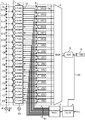
- FIG. 1 is a schematic configuration diagram of a power storage cell control device according to an exemplary embodiment.
- FIG. 2 is a circuit diagram illustrating a configuration example of a reference voltage portion group in FIG. 1 .
- FIG. 3 is a circuit diagram illustrating a circuit configuration example of a first ADC and a periphery thereof.
- FIG. 4 is a timing chart illustrating an operation example of the power storage cell control device according to the exemplary embodiment.
- FIG. 5 is a circuit diagram illustrating another circuit configuration example of the first ADC and the periphery thereof in FIG. 1 .
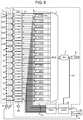
- FIG. 6 is a circuit diagram illustrating a system configuration example including the power storage cell control device according to the exemplary embodiment.
- FIG. 7 is a circuit diagram illustrating another configuration example of the power storage cell control device according to the exemplary embodiment.
- a power storage cell may be a cell having a function of storing power, and includes at least a battery cell and a capacitor cell.
- FIG. 1 is a diagram illustrating a schematic configuration of a power storage cell control device according to an exemplary embodiment.
- a plurality of power storage cells 1 a in FIG. 1 , sixteen power storage cells C 0 to C 15 ) are connected in series to each other.
- the power storage cell control device has a function of measuring a voltage of each of power storage cells 1 a in power storage module 1 .
- a lithium ion battery cell is used as power storage cell 1 a .
- the present exemplary embodiment is applicable to other kinds of power storage cells.
- the power storage cell control device includes ADC group 2 formed of a plurality of first analog-to-digital converters (ADC) 2 a , reference voltage portion group 3 formed of a plurality of first reference voltage portions 3 a which are respectively provided to correspond to first ADCs 2 a , multiplexer 4 as a selector, and second ADC 5 .
- the power storage cell control device also includes second reference voltage portion 6 which supplies reference potentials VRX+ and VRX ⁇ used as a criterion for a conversion operation of second ADC 5 , decimation filter 7 forming a voltage value acquirer, and calibration circuit 8 forming voltage value corrector.
- second reference voltage portion 6 is formed of a band gap circuit, a zener diode, or the like, and is adjusted (trimmed) during shipment inspection so as to supply a highly accurate absolute voltage criterion.
- Ammeter 9 measures current IO flowing through power storage module 1 .
- Each of first ADCs 2 a of ADC group 2 has a voltage of each of power storage cells 1 a as an input in power storage module 1 , and outputs first digital signal S 1 corresponding to the input.
- first ADC 2 a is a delta-sigma type ADC
- first digital signal S 1 which is an output thereof is a pulse density modulation (PDM) signal of 1 bit or a plurality of bits.
- PDM pulse density modulation
- Decimation filter 7 obtains a digital value indicating a voltage of power storage cell 1 a on the basis of first digital signal S 1 which is a PDM signal.
- a voltage level of a signal output from each first ADC 2 a is a voltage level of both ends of corresponding power storage cell 1 a , and thus signal output lines of respective first ADCs 2 a are provided with level shifters 12 for matching voltage levels of first digital signals S 1 with each other.
- a common clock signal generated by clock generator 10 is supplied to respective first ADCs 2 a which are thus operated in synchronization with the common clock signal.
- Each first reference voltage portion 3 a of reference voltage portion group 3 supplies reference potentials VRn+ and VRn ⁇ (where n is 0 to 15) used as a criterion for a conversion operation to corresponding first ADC 2 a .
- Potential differences between the reference potentials VRn+ and VRn ⁇ corresponding to respective first ADCs 2 a are the same as each other, but voltage levels thereof are set to correspond to voltage levels of anodes of respective power storage cells 1 a (or voltage levels thereof are set to correspond to voltage levels of power storage cells 1 a ).
- FIG. 2 illustrates a configuration example of reference voltage portion group 3 .
- each ADC 2 a is provided with first reference resistor 31 for supplying reference potentials VRn+ and VRn ⁇ .
- a current is generated by using a highly accurate reference voltage supplied by second reference voltage portion 6 and second reference resistor 32 , and the current is distributed via current mirror circuit 33 so as to flow through each first reference resistor 31 . Consequently, reference potentials VRn+ and VRn ⁇ are generated at both ends of first reference resistor 31 .
- FIG. 3 illustrates a circuit configuration example of first ADC 2 a and a periphery thereof.
- first ADC 2 a is a linear delta-sigma type ADC, and includes operational amplifier 21 and quantizer 22 .
- currents as distribution results obtained by using current mirror circuit 33 flow through first reference resistors 31 , and thus reference potentials VRn+ and VRn ⁇ are generated so as to be supplied to first ADCs 2 a.
- a voltage measured by first ADC 2 a is corrected on the basis of measured values of reference potentials VRn+ and VRn ⁇ , and thus a voltage of power storage cell 1 a can be obtained with high accuracy even if reference potentials VRn+ and VRn ⁇ do not have very high accuracy.
- multiplexer 4 selects reference potentials VRn+ and VRn ⁇ supplied by any one of respective first reference voltage portions 3 a of reference voltage portion group 3 , and supplies reference potentials VRn+ and VRn ⁇ to second ADC 5 as an input voltage.
- Second ADC 5 performs a conversion operation by using highly accurate reference potentials VRX+ and VRX ⁇ supplied from second reference voltage portion 6 as a criterion, and outputs second digital signal S 2 corresponding to the input voltage.
- second digital signal S 2 indicates differences between selected reference potentials VRn+ and VRn ⁇ and highly accurate reference potentials VRX+ and VRX ⁇ .
- Calibration circuit 8 receives second digital signal S 2 output from second ADC 5 , and corrects a voltage value of power storage cell 1 a obtained by decimation filter 7 on the basis of correction data obtained from second digital signal S 2 .
- calibration circuit 8 obtains a potential difference between reference potentials VRn+ and VRn ⁇ selected by multiplexer 4 on the basis of second digital signal S 2 .
- the correction data is obtained on the basis of a difference between the potential difference and a potential difference between highly accurate reference potentials VRX+ and VRX ⁇ stored in advance, and is stored.
- calibration circuit 8 stores correction data corresponding to each first reference voltage portion 3 a .
- the voltage value of power storage cell 1 a output from decimation filter 7 is corrected by using the stored correction data.
- a reference voltage used as a criterion for an AD conversion operation is the accuracy of a reference voltage used as a criterion for an AD conversion operation.
- a reference voltage for the ADC requires a highly accurate absolute voltage criterion having the accuracy of 2 to 10 ppm/° C. in terms of temperature stability and 0.02 to 0.1% in terms of absolute voltage error.
- first reference voltage portion 3 a even if the accuracy of reference potentials VRn+ and VRn ⁇ supplied by first reference voltage portion 3 a is not necessarily high, a correction process is performed on a voltage of power storage cell 1 a on the basis of highly accurate reference potentials VRX+ and VRX ⁇ , and thus it is possible to acquire a highly accurate value. Consequently, for example, a simple configuration illustrated in FIG. 2 can be employed in first reference voltage portion 3 a , and thus it is possible to prevent an increase in a circuit area or the number of work steps during shipment.
- FIG. 4 is a timing chart illustrating an example of an operation of the power storage cell control device according to the present exemplary embodiment.
- VC 0 to VC 15 indicate voltages of respective power storage cells C 0 to C 15 , and are measured by ADC group 2 .
- I 0 indicates a current flowing through power storage module 1 , and is measured by ammeter 9 .
- VR 0 to VR 15 indicate reference voltages for respective first ADCs 2 a, and are measured by second ADC 5 .
- voltages VC 0 to VC 15 of respective power storage cells C 0 to C 15 and current I 0 in power storage module 1 are measured in a cycle of, for example, 20 ⁇ s.
- Voltages VC 0 to VC 15 are corrected by calibration circuit 8 .
- reference voltages VR 0 to VR 15 for first ADCs 2 a are selected by multiplexer 4 in a cycle of, for example, 40 ⁇ s in a predetermined order, so as to be measured. Multiplexer 4 repeatedly performs this selection operation.
- Calibration circuit 8 updates correction data in the measurement cycle of reference voltages VR 0 to VR 15 for first ADCs 2 a . Thereafter, voltages VC 0 to VC 15 are corrected on the basis of updated correction data.
- reference voltages VR 0 to VR 15 are required to be performed in a cycle which is sufficiently shorter than a period of time in which reference voltages VR 0 to VR 15 change due to the influence of an environmental temperature or the like.
- the change in an environmental temperature is smooth relative to the measurement cycle of voltages of power storage cells C 0 to C 15 , and reference voltages VR 0 to VR 15 do not change suddenly.
- Reference voltages VR 0 to VR 15 is DC voltages with less disturbance noise unlike voltages of power storage cells 1 a .
- second ADC 5 has a high over-sampling rate, and thus it is possible to realize high resolution measurement.
- reference potentials VRn+ and VRn ⁇ for first ADC 2 a having a voltage of power storage cell 1 a as an input are measured by second ADC 5 which performs a conversion operation by using highly accurate reference potentials VRX+ and VRX ⁇ as a criterion.
- Decimation filter 7 generates a voltage value of power storage cell 1 a on the basis of first digital signal S 1 output from first ADC 2 a
- calibration circuit 8 corrects the voltage value by using correction data obtained from second digital signal S 2 output from second ADC 5 . Consequently, voltages of power storage cells 1 a can be measured with the accuracy of highly accurate reference potentials VRX+ and VRX ⁇ , and thus it is possible to minimize an error between voltage values of power storage cells 1 a.
- a plurality of first ADCs 2 a are provided to respectively correspond to power storage cells 1 a , and are operated in synchronization with the common clock signal, and thus it is possible to measure voltages of respective power storage cells 1 a at the same timing. Consequently, it is possible to measure a highly accurate SOC, SOH, or the like.
- first reference voltage portion 3 a can be formed of a relatively simple circuit.
- a circuit supplying a highly accurate absolute voltage criterion may be provided as first reference voltage portion 3 a in the same manner as second reference voltage portion 6 , but, in this case, a circuit area increases, and the number of trimming steps also considerably increases during shipment inspection.
- an output power value that is, a state of power (SOP) which is extracted from the power storage module can be obtained on the basis of an acquired SOC or SOH.
- SOP state of power
- the SOC has a linear correlation with an open voltage called an open circuit voltage (OCV), that is, a cell stable voltage in a state in which a current does not flow.
- OCV open circuit voltage
- a current flowing through the power storage module and a voltage of the power storage cell can be measured at the same timing, and thus the SOC can be computed on the basis of values thereof. Therefore, it is possible to understand a highly accurate SOC even with respect to a power storage module for an on-vehicle apparatus in which it is hard to obtain an OCV.
- First reference voltage portion 3 a may supply a power supply voltage and a ground voltage (GND voltage) to corresponding first ADC 2 a as reference potentials VRn+ and VRn ⁇ .
- FIG. 5 illustrates another circuit configuration example of first ADC 2 a and a periphery thereof, and illustrates a configuration in which a power supply voltage and a GND voltage for first ADC 2 a are also used as reference potentials VRn+ and VRn ⁇ .
- a repeated description of the substantially same portions as in FIGS. 1 and 2 will be omitted in some cases. As illustrated in FIG.
- FIG. 6 illustrates a configuration example of a power storage module management system including the power storage cell control device illustrated in FIG. 1 .
- ADC group 2 reference voltage portion group 3 , multiplexer 4 , second ADC 5 , second reference voltage portion 6 , decimation filter 7 , calibration circuit 8 , and the like are mounted on single semiconductor device 11 .
- Calculator 40 performs calculation of obtaining, for example, an SOC or an SOH on the basis of voltage value Dvc output from semiconductor device 11 and current value Di 0 obtained from ammeter 9 .
- a delta-sigma type ADC is employed as first ADC 2 a .
- a high over-sampling rate can be taken, and a specification required for an anti-aliasing filter can be lowered by reducing the order of a delta-sigma modulator to be used. Since a PDM signal of 1 bit or a plurality of bits is output, the number of digital signal up to decimation filter 7 in the subsequent stage can be reduced, and thus the number of level shifters 12 required for connection can be reduced.
- ADCs of types other than the delta-sigma type may be used as first ADC 2 a .
- an incremental type ADC it is possible to achieve the same effect as in the delta-sigma type.
- a successive approximation register (SAR; successive comparison) type ADC a cyclic type ADC, and a slope type ADC may be used.
- FIG. 7 illustrates another configuration example of the power storage cell control device according to the exemplary embodiment, and a SAR type ADC is used as first ADC 2 b forming ADC group 2 A.
- serial-parallel conversion circuit 7 A having digital signal S 1 A output from ADC 2 b as an input is provided as a voltage value acquirer.
- the SAR type ADC a digital value of an output signal is directly serially output, and thus the number of level shifters 12 required for connection to the subsequent stage can be reduced.
- the same effect can also be achieved in a cyclic type ADC or a slope type ADC.
- first ADC 2 a or 2 b is provided for each power storage cell 1 a in power storage module 1 , but any other configuration may be employed. In other words, the present exemplary embodiment may be applied to some of power storage cells 1 a of power storage module 1 .
- the power storage cell control device can measure voltages of a plurality of power storage cells in a power storage module at the same timing with high accuracy without increasing a circuit scale or the number of work steps during shipment, and is thus useful for reducing cost of, for example, an on-vehicle battery management system or improving accuracy.
Landscapes
- Engineering & Computer Science (AREA)
- Chemical & Material Sciences (AREA)
- Chemical Kinetics & Catalysis (AREA)
- Electrochemistry (AREA)
- General Chemical & Material Sciences (AREA)
- Manufacturing & Machinery (AREA)
- Power Engineering (AREA)
- Physics & Mathematics (AREA)
- General Physics & Mathematics (AREA)
- Microelectronics & Electronic Packaging (AREA)
- Secondary Cells (AREA)
- Measurement Of Current Or Voltage (AREA)
- Tests Of Electric Status Of Batteries (AREA)
Abstract
Description
- 1 power storage module
- 1 a power storage cell
- 2, 2A ADC group
- 2 a, 2 b first ADC
- 3 reference voltage portion group
- 3 a first reference voltage portion
- 4 multiplexer (selector)
- 5 second ADC
- 6 second reference voltage portion
- 7 decimation filter (voltage value acquirer)
- 7A serial-parallel conversion circuit (voltage value acquirer)
- 8 calibration circuit (voltage value corrector)
- 9 ammeter
- 11 semiconductor device
- 40 calculator
- S1 first digital signal
- S2 second digital signal
- VRn+, VRn− (where n is an integer), VRX+, VRX− reference potential
Claims (9)
Applications Claiming Priority (3)
| Application Number | Priority Date | Filing Date | Title |
|---|---|---|---|
| JP2014198575 | 2014-09-29 | ||
| JP2014-198575 | 2014-09-29 | ||
| PCT/JP2015/004582 WO2016051684A1 (en) | 2014-09-29 | 2015-09-09 | Storage cell control device and storage module management system |
Related Parent Applications (1)
| Application Number | Title | Priority Date | Filing Date |
|---|---|---|---|
| PCT/JP2015/004582 Continuation WO2016051684A1 (en) | 2014-09-29 | 2015-09-09 | Storage cell control device and storage module management system |
Publications (2)
| Publication Number | Publication Date |
|---|---|
| US20170184683A1 US20170184683A1 (en) | 2017-06-29 |
| US10698036B2 true US10698036B2 (en) | 2020-06-30 |
Family
ID=55629761
Family Applications (1)
| Application Number | Title | Priority Date | Filing Date |
|---|---|---|---|
| US15/454,191 Active 2037-11-01 US10698036B2 (en) | 2014-09-29 | 2017-03-09 | Power storage cell control device and power storage module management system |
Country Status (4)
| Country | Link |
|---|---|
| US (1) | US10698036B2 (en) |
| EP (1) | EP3203246B1 (en) |
| JP (1) | JPWO2016051684A1 (en) |
| WO (1) | WO2016051684A1 (en) |
Cited By (4)
| Publication number | Priority date | Publication date | Assignee | Title |
|---|---|---|---|---|
| US11502530B2 (en) * | 2017-12-26 | 2022-11-15 | Panasonic Intellectual Property Management Co., Ltd. | Battery management device, battery system, and vehicle power supply system for managing battery state of charge level when in non-use state |
| US20230344262A1 (en) * | 2022-04-25 | 2023-10-26 | Apple Inc. | System and method for variable discharging techniques of a battery cell |
| EP4372993A1 (en) * | 2022-11-15 | 2024-05-22 | Hyundai Mobis Co., Ltd. | Apparatus for measuring voltage |
| US20240272228A1 (en) * | 2023-02-10 | 2024-08-15 | Relyion Energy, Inc. | Voltage transducer |
Families Citing this family (5)
| Publication number | Priority date | Publication date | Assignee | Title |
|---|---|---|---|---|
| JP2015155859A (en) * | 2014-02-21 | 2015-08-27 | ソニー株式会社 | Battery remaining amount estimating device, battery pack, power storage device, electric vehicle, and battery remaining amount estimating method |
| WO2018230187A1 (en) * | 2017-06-14 | 2018-12-20 | 日立オートモティブシステムズ株式会社 | Battery monitoring device |
| JP7213187B2 (en) * | 2017-08-29 | 2023-01-26 | ヌヴォトンテクノロジージャパン株式会社 | Voltage detection circuit |
| US10901045B2 (en) | 2018-03-16 | 2021-01-26 | Infineon Technologies Ag | Battery diagnostics system and method using second path redundant measurement approach |
| WO2025115506A1 (en) * | 2023-11-30 | 2025-06-05 | Fdk株式会社 | Battery management system, management device, cycle setting method, and program |
Citations (12)
| Publication number | Priority date | Publication date | Assignee | Title |
|---|---|---|---|---|
| JPH11109005A (en) | 1997-09-30 | 1999-04-23 | Matsushita Electric Ind Co Ltd | Battery voltage measuring device |
| JPH11160367A (en) | 1997-11-26 | 1999-06-18 | Denso Corp | Voltage detector for assembled batteries for electric vehicles |
| US6313637B1 (en) | 1997-11-20 | 2001-11-06 | Denso Corporation | Voltage detecting device for set battery |
| JP2002156392A (en) | 2000-11-20 | 2002-05-31 | Denso Corp | Battery voltage detector |
| US20060007622A1 (en) | 2004-07-06 | 2006-01-12 | Kimihiko Furukawa | Car power source apparatus |
| JP2009198448A (en) | 2008-02-25 | 2009-09-03 | Yazaki Corp | Voltage detector |
| JP2011158268A (en) | 2010-01-29 | 2011-08-18 | Mitsumi Electric Co Ltd | Apparatus and method for calculating smooth current, and battery monitoring module |
| WO2012153372A1 (en) | 2011-05-10 | 2012-11-15 | パナソニック株式会社 | Successive approximation type a/d converter |
| US20120326725A1 (en) | 2011-06-24 | 2012-12-27 | Sony Corporation | Monitoring apparatus, monitoring control apparatus, power supply apparatus, monitoring method, monitoring control method, power storage system, electronic apparatus, motor-driven vehicle, and electric power system |
| US20130057289A1 (en) * | 2010-05-28 | 2013-03-07 | Yazaki Corporation | Voltage measuring apparatus for battery assembly |
| US20130234720A1 (en) | 2012-03-07 | 2013-09-12 | Mitsumi Electric Co., Ltd. | Battery voltage monitor circuit |
| US8723527B2 (en) * | 2009-02-27 | 2014-05-13 | Hitachi, Ltd. | Battery monitoring system |
-
2015
- 2015-09-09 WO PCT/JP2015/004582 patent/WO2016051684A1/en not_active Ceased
- 2015-09-09 JP JP2016551498A patent/JPWO2016051684A1/en active Pending
- 2015-09-09 EP EP15846434.7A patent/EP3203246B1/en active Active
-
2017
- 2017-03-09 US US15/454,191 patent/US10698036B2/en active Active
Patent Citations (17)
| Publication number | Priority date | Publication date | Assignee | Title |
|---|---|---|---|---|
| JPH11109005A (en) | 1997-09-30 | 1999-04-23 | Matsushita Electric Ind Co Ltd | Battery voltage measuring device |
| US6313637B1 (en) | 1997-11-20 | 2001-11-06 | Denso Corporation | Voltage detecting device for set battery |
| JPH11160367A (en) | 1997-11-26 | 1999-06-18 | Denso Corp | Voltage detector for assembled batteries for electric vehicles |
| JP2002156392A (en) | 2000-11-20 | 2002-05-31 | Denso Corp | Battery voltage detector |
| US20060007622A1 (en) | 2004-07-06 | 2006-01-12 | Kimihiko Furukawa | Car power source apparatus |
| JP2006025501A (en) | 2004-07-06 | 2006-01-26 | Sanyo Electric Co Ltd | Power supply for vehicle |
| JP2009198448A (en) | 2008-02-25 | 2009-09-03 | Yazaki Corp | Voltage detector |
| US8723527B2 (en) * | 2009-02-27 | 2014-05-13 | Hitachi, Ltd. | Battery monitoring system |
| JP2011158268A (en) | 2010-01-29 | 2011-08-18 | Mitsumi Electric Co Ltd | Apparatus and method for calculating smooth current, and battery monitoring module |
| US20120296587A1 (en) | 2010-01-29 | 2012-11-22 | Ren Sugiyama | Smooth current calculation apparatus, smooth current calculation method and battery monitoring module |
| US20130057289A1 (en) * | 2010-05-28 | 2013-03-07 | Yazaki Corporation | Voltage measuring apparatus for battery assembly |
| WO2012153372A1 (en) | 2011-05-10 | 2012-11-15 | パナソニック株式会社 | Successive approximation type a/d converter |
| US8947290B2 (en) | 2011-05-10 | 2015-02-03 | Panasonic Intellectual Property Management Co., Ltd. | Successive approximation AD converter |
| JP2013009514A (en) | 2011-06-24 | 2013-01-10 | Sony Corp | Monitoring apparatus, monitoring control apparatus, power supply apparatus, monitoring method, monitoring control method, power storage system, electronic apparatus, motor-driven vehicle, and electric power system |
| US20120326725A1 (en) | 2011-06-24 | 2012-12-27 | Sony Corporation | Monitoring apparatus, monitoring control apparatus, power supply apparatus, monitoring method, monitoring control method, power storage system, electronic apparatus, motor-driven vehicle, and electric power system |
| US20130234720A1 (en) | 2012-03-07 | 2013-09-12 | Mitsumi Electric Co., Ltd. | Battery voltage monitor circuit |
| JP2013185904A (en) | 2012-03-07 | 2013-09-19 | Mitsumi Electric Co Ltd | Battery voltage monitoring circuit |
Non-Patent Citations (1)
| Title |
|---|
| International Search Report of PCT application No. PCT/JP2015/004582 dated Dec. 15, 2015. |
Cited By (6)
| Publication number | Priority date | Publication date | Assignee | Title |
|---|---|---|---|---|
| US11502530B2 (en) * | 2017-12-26 | 2022-11-15 | Panasonic Intellectual Property Management Co., Ltd. | Battery management device, battery system, and vehicle power supply system for managing battery state of charge level when in non-use state |
| US20230344262A1 (en) * | 2022-04-25 | 2023-10-26 | Apple Inc. | System and method for variable discharging techniques of a battery cell |
| EP4372993A1 (en) * | 2022-11-15 | 2024-05-22 | Hyundai Mobis Co., Ltd. | Apparatus for measuring voltage |
| US12248007B2 (en) | 2022-11-15 | 2025-03-11 | Hyundai Mobis Co., Ltd. | Apparatus for measuring voltage |
| US20240272228A1 (en) * | 2023-02-10 | 2024-08-15 | Relyion Energy, Inc. | Voltage transducer |
| US12596153B2 (en) * | 2023-02-10 | 2026-04-07 | Relyion Energy Inc. | Voltage transducer |
Also Published As
| Publication number | Publication date |
|---|---|
| EP3203246B1 (en) | 2018-11-14 |
| EP3203246A4 (en) | 2017-10-11 |
| EP3203246A1 (en) | 2017-08-09 |
| US20170184683A1 (en) | 2017-06-29 |
| JPWO2016051684A1 (en) | 2017-08-10 |
| WO2016051684A1 (en) | 2016-04-07 |
Similar Documents
| Publication | Publication Date | Title |
|---|---|---|
| US10698036B2 (en) | Power storage cell control device and power storage module management system | |
| JP6775625B2 (en) | Battery diagnostic systems and methods that use a redundant measurement approach with a second path | |
| CN107037329B (en) | Insulation abnormality detection device and insulation abnormality detection method | |
| US10295600B2 (en) | Monitoring charge stored in a battery | |
| US10429450B2 (en) | Battery sensing method and apparatus | |
| CN104272125B (en) | Battery monitoring apparatus and battery system monitoring arrangement | |
| JP6182025B2 (en) | Battery health estimation device and health estimation method | |
| CN103580694B (en) | System and device for determining voltage | |
| EP2843431B1 (en) | Battery monitoring device and battery system monitoring device | |
| US10534022B2 (en) | Analogue measurement data detection system and battery voltage detection system | |
| US8283894B2 (en) | Voltage measuring apparatus for assembled battery | |
| US9419644B2 (en) | System, circuit and method for converting a differential voltage signal including a high common mode voltage component to a ground referenced signal for battery voltage managment | |
| WO2013168349A1 (en) | Device for estimating state of charge of battery | |
| US9362938B2 (en) | Error measurement and calibration of analog to digital converters | |
| US11536773B2 (en) | Digital correction algorithms to improve battery voltage measurement accuracy | |
| JP5700756B2 (en) | Voltage measurement device for multiple assembled batteries | |
| US10042005B2 (en) | Internal resistance calculating device | |
| US11888494B2 (en) | Semiconductor integrated circuit | |
| CN102545906A (en) | Current digital to analog conversion method and device | |
| KR20170141035A (en) | Low cost impedance spectroscopy system and method capable of estimating state of health for high-voltage battery pack | |
| KR101457923B1 (en) | Battery cell voltage measuring apparatus with automatic correction function and method thereof | |
| KR102935149B1 (en) | Battery monitoring techniques | |
| EP4380059A1 (en) | Internally calibrated analog-to-digital converter | |
| JP2013015334A (en) | Battery voltage detection system | |
| US11656252B2 (en) | Method for measuring current and measurement apparatus |
Legal Events
| Date | Code | Title | Description |
|---|---|---|---|
| AS | Assignment |
Owner name: PANASONIC INTELLECTUAL PROPERTY MANAGEMENT CO., LTD., JAPAN Free format text: ASSIGNMENT OF ASSIGNORS INTEREST;ASSIGNOR:KOBAYASHI, HITOSHI;REEL/FRAME:041790/0636 Effective date: 20170131 Owner name: PANASONIC INTELLECTUAL PROPERTY MANAGEMENT CO., LT Free format text: ASSIGNMENT OF ASSIGNORS INTEREST;ASSIGNOR:KOBAYASHI, HITOSHI;REEL/FRAME:041790/0636 Effective date: 20170131 |
|
| STPP | Information on status: patent application and granting procedure in general |
Free format text: DOCKETED NEW CASE - READY FOR EXAMINATION |
|
| STPP | Information on status: patent application and granting procedure in general |
Free format text: NOTICE OF ALLOWANCE MAILED -- APPLICATION RECEIVED IN OFFICE OF PUBLICATIONS |
|
| STPP | Information on status: patent application and granting procedure in general |
Free format text: PUBLICATIONS -- ISSUE FEE PAYMENT RECEIVED |
|
| AS | Assignment |
Owner name: PANASONIC SEMICONDUCTOR SOLUTIONS CO., LTD., JAPAN Free format text: ASSIGNMENT OF ASSIGNORS INTEREST;ASSIGNOR:PANASONIC INTELLECTUAL PROPERTY MANAGEMENT CO., LTD.;REEL/FRAME:052755/0870 Effective date: 20200521 |
|
| STCF | Information on status: patent grant |
Free format text: PATENTED CASE |
|
| MAFP | Maintenance fee payment |
Free format text: PAYMENT OF MAINTENANCE FEE, 4TH YEAR, LARGE ENTITY (ORIGINAL EVENT CODE: M1551); ENTITY STATUS OF PATENT OWNER: LARGE ENTITY Year of fee payment: 4 |