EP4372336B1 - Messsystem und verfahren dafür - Google Patents
Messsystem und verfahren dafür Download PDFInfo
- Publication number
- EP4372336B1 EP4372336B1 EP23210588.2A EP23210588A EP4372336B1 EP 4372336 B1 EP4372336 B1 EP 4372336B1 EP 23210588 A EP23210588 A EP 23210588A EP 4372336 B1 EP4372336 B1 EP 4372336B1
- Authority
- EP
- European Patent Office
- Prior art keywords
- temperature
- chip
- pair
- junction
- temperature measurement
- Prior art date
- Legal status (The legal status is an assumption and is not a legal conclusion. Google has not performed a legal analysis and makes no representation as to the accuracy of the status listed.)
- Active
Links
Images


Classifications
-
- G—PHYSICS
- G01—MEASURING; TESTING
- G01K—MEASURING TEMPERATURE; MEASURING QUANTITY OF HEAT; THERMALLY-SENSITIVE ELEMENTS NOT OTHERWISE PROVIDED FOR
- G01K7/00—Measuring temperature based on the use of electric or magnetic elements directly sensitive to heat ; Power supply therefor, e.g. using thermoelectric elements
- G01K7/01—Measuring temperature based on the use of electric or magnetic elements directly sensitive to heat ; Power supply therefor, e.g. using thermoelectric elements using semiconducting elements having PN junctions
- G01K7/015—Measuring temperature based on the use of electric or magnetic elements directly sensitive to heat ; Power supply therefor, e.g. using thermoelectric elements using semiconducting elements having PN junctions using microstructures, e.g. made of silicon
-
- G—PHYSICS
- G01—MEASURING; TESTING
- G01K—MEASURING TEMPERATURE; MEASURING QUANTITY OF HEAT; THERMALLY-SENSITIVE ELEMENTS NOT OTHERWISE PROVIDED FOR
- G01K13/00—Thermometers specially adapted for specific purposes
- G01K13/20—Clinical contact thermometers for use with humans or animals
- G01K13/223—Infrared clinical thermometers, e.g. tympanic
-
- G—PHYSICS
- G01—MEASURING; TESTING
- G01K—MEASURING TEMPERATURE; MEASURING QUANTITY OF HEAT; THERMALLY-SENSITIVE ELEMENTS NOT OTHERWISE PROVIDED FOR
- G01K7/00—Measuring temperature based on the use of electric or magnetic elements directly sensitive to heat ; Power supply therefor, e.g. using thermoelectric elements
- G01K7/02—Measuring temperature based on the use of electric or magnetic elements directly sensitive to heat ; Power supply therefor, e.g. using thermoelectric elements using thermoelectric elements, e.g. thermocouples
-
- G—PHYSICS
- G01—MEASURING; TESTING
- G01J—MEASUREMENT OF INTENSITY, VELOCITY, SPECTRAL CONTENT, POLARISATION, PHASE OR PULSE CHARACTERISTICS OF INFRARED, VISIBLE OR ULTRAVIOLET LIGHT; COLORIMETRY; RADIATION PYROMETRY
- G01J5/00—Radiation pyrometry, e.g. infrared or optical thermometry
- G01J5/0003—Radiation pyrometry, e.g. infrared or optical thermometry for sensing the radiant heat transfer of samples, e.g. emittance meter
- G01J5/0011—Ear thermometers
-
- G—PHYSICS
- G01—MEASURING; TESTING
- G01J—MEASUREMENT OF INTENSITY, VELOCITY, SPECTRAL CONTENT, POLARISATION, PHASE OR PULSE CHARACTERISTICS OF INFRARED, VISIBLE OR ULTRAVIOLET LIGHT; COLORIMETRY; RADIATION PYROMETRY
- G01J5/00—Radiation pyrometry, e.g. infrared or optical thermometry
- G01J5/02—Constructional details
- G01J5/06—Arrangements for eliminating effects of disturbing radiation; Arrangements for compensating changes in sensitivity
- G01J5/061—Arrangements for eliminating effects of disturbing radiation; Arrangements for compensating changes in sensitivity by controlling the temperature of the apparatus or parts thereof, e.g. using cooling means or thermostats
-
- G—PHYSICS
- G01—MEASURING; TESTING
- G01J—MEASUREMENT OF INTENSITY, VELOCITY, SPECTRAL CONTENT, POLARISATION, PHASE OR PULSE CHARACTERISTICS OF INFRARED, VISIBLE OR ULTRAVIOLET LIGHT; COLORIMETRY; RADIATION PYROMETRY
- G01J5/00—Radiation pyrometry, e.g. infrared or optical thermometry
- G01J5/02—Constructional details
- G01J5/06—Arrangements for eliminating effects of disturbing radiation; Arrangements for compensating changes in sensitivity
- G01J5/064—Ambient temperature sensor; Housing temperature sensor; Constructional details thereof
-
- G—PHYSICS
- G01—MEASURING; TESTING
- G01J—MEASUREMENT OF INTENSITY, VELOCITY, SPECTRAL CONTENT, POLARISATION, PHASE OR PULSE CHARACTERISTICS OF INFRARED, VISIBLE OR ULTRAVIOLET LIGHT; COLORIMETRY; RADIATION PYROMETRY
- G01J5/00—Radiation pyrometry, e.g. infrared or optical thermometry
- G01J5/10—Radiation pyrometry, e.g. infrared or optical thermometry using electric radiation detectors
- G01J5/12—Radiation pyrometry, e.g. infrared or optical thermometry using electric radiation detectors using thermoelectric elements, e.g. thermocouples
-
- G—PHYSICS
- G01—MEASURING; TESTING
- G01K—MEASURING TEMPERATURE; MEASURING QUANTITY OF HEAT; THERMALLY-SENSITIVE ELEMENTS NOT OTHERWISE PROVIDED FOR
- G01K3/00—Thermometers giving results other than momentary value of temperature
- G01K3/08—Thermometers giving results other than momentary value of temperature giving differences of values; giving differentiated values
-
- G—PHYSICS
- G01—MEASURING; TESTING
- G01K—MEASURING TEMPERATURE; MEASURING QUANTITY OF HEAT; THERMALLY-SENSITIVE ELEMENTS NOT OTHERWISE PROVIDED FOR
- G01K7/00—Measuring temperature based on the use of electric or magnetic elements directly sensitive to heat ; Power supply therefor, e.g. using thermoelectric elements
- G01K7/01—Measuring temperature based on the use of electric or magnetic elements directly sensitive to heat ; Power supply therefor, e.g. using thermoelectric elements using semiconducting elements having PN junctions
-
- G—PHYSICS
- G01—MEASURING; TESTING
- G01K—MEASURING TEMPERATURE; MEASURING QUANTITY OF HEAT; THERMALLY-SENSITIVE ELEMENTS NOT OTHERWISE PROVIDED FOR
- G01K7/00—Measuring temperature based on the use of electric or magnetic elements directly sensitive to heat ; Power supply therefor, e.g. using thermoelectric elements
- G01K7/02—Measuring temperature based on the use of electric or magnetic elements directly sensitive to heat ; Power supply therefor, e.g. using thermoelectric elements using thermoelectric elements, e.g. thermocouples
- G01K7/021—Particular circuit arrangements
-
- G—PHYSICS
- G01—MEASURING; TESTING
- G01K—MEASURING TEMPERATURE; MEASURING QUANTITY OF HEAT; THERMALLY-SENSITIVE ELEMENTS NOT OTHERWISE PROVIDED FOR
- G01K7/00—Measuring temperature based on the use of electric or magnetic elements directly sensitive to heat ; Power supply therefor, e.g. using thermoelectric elements
- G01K7/02—Measuring temperature based on the use of electric or magnetic elements directly sensitive to heat ; Power supply therefor, e.g. using thermoelectric elements using thermoelectric elements, e.g. thermocouples
- G01K7/028—Measuring temperature based on the use of electric or magnetic elements directly sensitive to heat ; Power supply therefor, e.g. using thermoelectric elements using thermoelectric elements, e.g. thermocouples using microstructures, e.g. made of silicon
-
- G—PHYSICS
- G01—MEASURING; TESTING
- G01K—MEASURING TEMPERATURE; MEASURING QUANTITY OF HEAT; THERMALLY-SENSITIVE ELEMENTS NOT OTHERWISE PROVIDED FOR
- G01K7/00—Measuring temperature based on the use of electric or magnetic elements directly sensitive to heat ; Power supply therefor, e.g. using thermoelectric elements
- G01K7/16—Measuring temperature based on the use of electric or magnetic elements directly sensitive to heat ; Power supply therefor, e.g. using thermoelectric elements using resistive elements
- G01K7/22—Measuring temperature based on the use of electric or magnetic elements directly sensitive to heat ; Power supply therefor, e.g. using thermoelectric elements using resistive elements the element being a non-linear resistance, e.g. thermistor
- G01K7/24—Measuring temperature based on the use of electric or magnetic elements directly sensitive to heat ; Power supply therefor, e.g. using thermoelectric elements using resistive elements the element being a non-linear resistance, e.g. thermistor in a specially-adapted circuit, e.g. bridge circuit
-
- G—PHYSICS
- G01—MEASURING; TESTING
- G01J—MEASUREMENT OF INTENSITY, VELOCITY, SPECTRAL CONTENT, POLARISATION, PHASE OR PULSE CHARACTERISTICS OF INFRARED, VISIBLE OR ULTRAVIOLET LIGHT; COLORIMETRY; RADIATION PYROMETRY
- G01J5/00—Radiation pyrometry, e.g. infrared or optical thermometry
- G01J5/02—Constructional details
- G01J5/06—Arrangements for eliminating effects of disturbing radiation; Arrangements for compensating changes in sensitivity
- G01J5/061—Arrangements for eliminating effects of disturbing radiation; Arrangements for compensating changes in sensitivity by controlling the temperature of the apparatus or parts thereof, e.g. using cooling means or thermostats
- G01J2005/063—Heating; Thermostating
-
- G—PHYSICS
- G01—MEASURING; TESTING
- G01J—MEASUREMENT OF INTENSITY, VELOCITY, SPECTRAL CONTENT, POLARISATION, PHASE OR PULSE CHARACTERISTICS OF INFRARED, VISIBLE OR ULTRAVIOLET LIGHT; COLORIMETRY; RADIATION PYROMETRY
- G01J5/00—Radiation pyrometry, e.g. infrared or optical thermometry
- G01J5/10—Radiation pyrometry, e.g. infrared or optical thermometry using electric radiation detectors
- G01J5/12—Radiation pyrometry, e.g. infrared or optical thermometry using electric radiation detectors using thermoelectric elements, e.g. thermocouples
- G01J5/14—Electrical features thereof
-
- G—PHYSICS
- G01—MEASURING; TESTING
- G01J—MEASUREMENT OF INTENSITY, VELOCITY, SPECTRAL CONTENT, POLARISATION, PHASE OR PULSE CHARACTERISTICS OF INFRARED, VISIBLE OR ULTRAVIOLET LIGHT; COLORIMETRY; RADIATION PYROMETRY
- G01J5/00—Radiation pyrometry, e.g. infrared or optical thermometry
- G01J5/80—Calibration
-
- G—PHYSICS
- G01—MEASURING; TESTING
- G01K—MEASURING TEMPERATURE; MEASURING QUANTITY OF HEAT; THERMALLY-SENSITIVE ELEMENTS NOT OTHERWISE PROVIDED FOR
- G01K2217/00—Temperature measurement using electric or magnetic components already present in the system to be measured
Definitions
- the present disclosure relates to chips, systems and methods for use in temperature sensing and temperature measurement, and more particularly to a sensing chip using a device made with a semiconductor manufacturing process to sense a target temperature, a measuring chip operating in conjunction with the sensing chip, a temperature difference measurement system for measuring the sensing chip and the measuring chip, a temperature measurement system and method using the temperature difference measurement system, and a computer program product thereof.
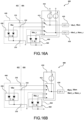
- the conventional temperature measurement system 100 comprises a driving chip 120, a thermopile device 112 and a thermistor 114, wherein the thermopile device 112 senses a target temperature, the thermistor 114 directly senses the ambient temperature of the thermopile device 112.
- the driving chip 120 comprises a target temperature measurement circuit 122, a temperature measurement circuit 124 and a central processing unit (CPU) 126, wherein the target temperature measurement circuit 122 is electrically connected to the thermopile device 112 to measure a first voltage signal associated with the target temperature.
- the temperature measurement circuit 124 is electrically connected to the thermistor 114 to measure a second voltage signal associated with the ambient temperature.
- the CPU 126 receives the first and second voltage signals to calculate the target temperature sensed by the thermopile device 112.
- the thermopile device 112 is a silicon transducer.
- the silicon transducer is manufactured by a silicon process and a semiconductor manufacturing process. With the silicon transducer being manufactured by a semiconductor manufacturing process, the manifestation of its characteristics and physical quantity must be affected by temperature.
- FIG. 1B there is shown a graph of a voltage signal of the thermopile device 112 versus a target temperature, measured with the target temperature measurement circuit 122 at different ambient temperatures 0°C, 25°C and 37°C.
- the ideal thermopile equation shows that the output voltage of the thermopile device 112 is directly proportional to the difference between the fourth power of the target temperature T t 4 and the fourth power of the ambient temperature T a 4 . Therefore, the output voltage of the thermopile device 112 and the target temperature T t , as measured by the target temperature measurement circuit 122, have a nonlinear relation. In other words, the ideal thermopile equation also shows that a nonlinear relation of the output voltage varies with the ambient temperature T a . The nonlinear relation of the output voltage is even more obvious in the presence of a large difference between the ambient temperature T a of the silicon transducer and the target temperature T t to be measured.
- the temperature measurement system 100 does not calibrate the output voltage of the silicon transducer, errors of the temperature values will increase. Thus, the CPU 126 has to be informed of the ambient temperature of the thermopile device 112 in order to calibrate the calculated target temperature to ensure accurate temperature measurement.
- the thermistor 114 is a temperature sensor commonly used in temperature measurement. However, the thermistor 114 is a self-contained component, whereas the thermopile device 112 is a silicon transducer manufactured by a silicon process and a semiconductor manufacturing process. Due to the different manufacturing processes, the thermistor 114 cannot be integrated with the silicon transducer using semiconductor manufacturing process, but can be placed inside the same package by packaging technology.
- the driving chip 120 operates in conjunction with the thermopile device 112 and the thermistor 114, and the target temperature and the measurement results of the thermistor also have a nonlinear relation, and thus these factors requires a calibration by the system to enhance the accuracy of the measurement results. As a result, these factors will result in difficulties in mass production due to the additional calibration procedures.
- US2021/364359 A1 discloses an infrared temperature sensor comprising a package substrate, a thermopile sensing chip attached to the package substrate, a cap, and a filter.
- the thermopile sensing chip includes a chip substrate, a thermopile sensing unit, a heater, and at least a temperature sensing element. The heater maintains the cold end of the thermopile sensing unit at a pre-set working temperature thereby enabling single-point temperature calibration.
- DE10341142 A1 discloses a body temperature radiation thermometer comprising a cylindrical housing, a thermopile sensor at the tapered end of the housing, a sensor housing, a sensor housing cap, a sensor housing bottom, an infrared thermopile sensor on the sensor housing bottom, a heater on the sensor housing bottom, an electrical connection between the thermopile sensor and a measuring electronics circuit board, a plurality of temperature sensors.
- the measured values of the temperature sensors are used to calculate temperature differences between them and thereby to determine instantaneous temperature gradients within the sensor housing.
- US6890097 B2 discloses a semiconductor device comprising a silicon substrate, a main circuit section, a temperature measuring sensor comprising a p-n junction diode, a temperature calibration circuit, and an additional temperature measuring sensor comprising a p-n junction diode.
- US 2009/207882 A1 discloses a first temperature sensor being a thermal diode, a second temperature sensor being a thermopile or a CMOS-infrared temperature sensor, a third temperature sensor, wherein the second temperature sensor and the third temperature sensor are integrated on a substrate to form a single-chip temperature module.
- US8061894 B2 discloses a semiconductor device comprising n pieces of semiconductor chip, wherein each semiconductor chip is mounted with a temperature detection circuit.
- Each temperature detection circuit has its output terminal commonly connected to out output terminal.
- an average value of the temperatures of the individual semiconductor chips is detected.
- the highest temperature from among all the semiconductor chips is detected.
- the lowest temperature from among all the semiconductor chips is detected.
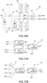
- FIG. 2A there is shown a block diagram of another conventional temperature measurement system 100 including a sensing chip.
- the conventional temperature measurement system 100 comprises a driving chip 120 and a sensing chip 110.
- the driving chip 120 comprises a target temperature measurement circuit 122, a temperature measurement circuit 124 and a CPU 126.
- the thermopile device 112 and a diode 116 are integrated into the sensing chip 110 by a semiconductor manufacturing process.
- the diode 116 functions as a heat sensor for directly measuring the ambient temperature of the thermopile device 112. Since the driving chip 120 and the sensing chip 110 are electrically connected, the target temperature measurement circuit 122 of the driving chip 120 is electrically connected to the thermopile device 112, and the temperature measurement circuit 124 of the driving chip 120 is electrically connected to the diode 116.
- the diode 116 and the silicon transducer can be integrated by a semiconductor manufacturing process, the manifestation of the characteristics and physical quantity of the silicon transducer is still affected by temperature. If the temperature measurement system 100 does not calibrate the output voltage of the silicon transducer, the error of the temperature difference measurement would be increased. From the perspective of the driving chip 120, the diode 116 of the sensing chip 110 is an external component, and thus the driving chip 120 cannot calibrate the diode 116 in the course of chip production, and the mass production of integrated products would be difficult because of an extra calibration procedure to enhance the accuracy of the measurement results.
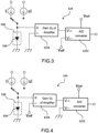
- FIG. 3 and FIG. 4 there are shown circuit diagrams of the external diode 116 measured with two conventional temperature measurement circuits 124 of the driving chip 120 shown in FIG. 2A , respectively.
- the conventional temperature measurement circuits 124 of the driving chip 120 measure absolute temperature starting from 0°K, as shown in FIG. 2B .
- the room temperature 27°C is around 300°K and ranges between 10°C (283°K) and 50°C (323°K).
- Accuracy of 0.01°K requires 30000 count stable resolution, corresponding to the A/D converter specification of 16-bit stability to only allow the last bit jitter, which is a very strict specification for A/D converters and also required high signal noise suppression.
- the driving chip directly measures the external diode; as a result, the temperature is too wide, and the accuracy is low. Furthermore, the external diode 116 of the sensing chip 110 is an arbitrary choice for system manufacturers, and thus manufacturers of the driving chip 120 cannot accurately calibrate the external diode, leading to considerable measurement errors.
- the conventional temperature measurement circuit 124 shown in FIG. 3 measures the diode 116 of the sensing chip 110, it switches between two current sources ( I , n I ) with an electronic switch.
- the temperature measurement range is 0 ⁇ 400 °K (absolute temperature), starting from 0°K.
- the first instance of measurement requires the electronic switch to switch to current source I , causing the external diode 116 to generate a voltage V BE1 .
- the second instance of measurement requires the electronic switch to switch to current source n I , causing the external diode 116 to generate a voltage V BE n .
- the voltages V BEn , V BE1 are measured with an A/D converter.
- the CPU 126 subtracts one of the two ADC values from the other to obtain a value corresponding to ⁇ V BE .
- the value is directly proportional to absolute temperature, as shown in FIG. 2B . Since voltage V BE is large and greater than voltage V ref , the subtraction therefrom of a voltage V off or reduction of amplifier gain G 2 has to be carried out to enter the measurement range of the A/D converter.
- ADC n V BEn ⁇ G 2 ⁇ V off V ref
- ADC 1 V BE 1 ⁇ G 2 ⁇ V off V ref
- V ref K cal 2 ⁇ T
- G 2 denotes amplification ratio (0.5-2)
- V ref denotes A/D converter reference voltage
- V off denotes A/D converter offset voltage.
- V ref ⁇ V BE ⁇ G 3
- V ref K cal 3 ⁇ T
- G 3 denotes amplification ratio (2 ⁇ 10)
- V ref denotes reference voltage of A/D converter
- V off denotes offset voltage of amplifier
- the driving chip 120 directly measures the diode 116 of an external heat sensor with the temperature measurement circuit 124 shown in FIG. 3 and FIG. 4 , the temperature measurement accuracy is insufficient.
- one objective of the present disclosure is to provide a technical solution for integrating the silicon transducer and a heater into a semiconductor substrate, and to use the heater to heat the semiconductor substrate so that the silicon transducer can operate at a predetermined temperature for obtaining stable transducing characteristics.
- the heater is configured to have the ambient temperature of the thermopile device approach a target temperature, such that temperature measurement results and the target temperature approximate a linear relationship.
- a conventional sensing chip is characterized by the integration of a thermopile device and a diode into a semiconductor substrate.
- the diode directly measures the ambient temperature of the thermopile device.
- a temperature measurement circuit for driving the sensing chip has to be integrated into a system product and then an additional calibration of the ambient temperature measured with the external diode is required, resulting in difficulties to carry out mass production and to enhance the accuracy of measurement.
- thermopile device and at least one diode into a sensing chip, measuring the temperature difference between the sensing chip and a measuring chip (or driving chip) with the at least one diode, and allowing the measurement result of the measuring chip (or driving chip) to be calibrated prior to the system product integration, so as to render it possible to carry out mass production and enhance the accuracy of measurement.
- the present disclosure provides a sensing chip integrated into a semiconductor substrate with a silicon transducer and at least one heater, wherein the silicon transducer and the heater are electrically connected to a measuring chip respectively, so that the measuring chip provides an electrical energy to the heater for heating the temperature of the semiconductor substrate, and the measuring chip measures the difference between the temperature of an object under test and the temperature of the semiconductor substrate by the silicon transducer.
- the present disclosure provides a method of manufacturing a sensing chip, comprising the steps of: forming a silicon transducer on a semiconductor substrate by a semiconductor manufacturing process; and forming at least one heater on the semiconductor substrate by the semiconductor manufacturing process, wherein the silicon transducer and the heater are electrically connected to a measuring chip respectively, so that the measuring chip provides an electrical energy to the heater for heating the temperature of the semiconductor substrate, and the measuring chip measures the difference between the temperature of an object under test and the temperature of the semiconductor substrate by the silicon transducer.
- the present disclosure provides a method of manufacturing a measuring chip, comprising the steps of: forming a plurality of nodes on a semiconductor substrate by a semiconductor manufacturing process, wherein at least one portion of the nodes is electrically connected to a sensing chip; forming a heating circuit on the semiconductor substrate by the semiconductor manufacturing process, wherein the heating circuit provides an electrical energy to a heater of the sensing chip through at least one portion of the nodes; and forming a first temperature measurement circuit on the semiconductor substrate by the semiconductor manufacturing process, the first temperature measurement circuit is electrically connected to a silicon transducer of the sensing chip through at least one portion of the nodes, wherein the first temperature measurement circuit measures the difference between the temperature of an object under test and the temperature of the sensing chip by the silicon transducer.
- the present disclosure provides a temperature measurement system electrically connected to a sensing chip, the sensing chip comprising at least one heater and a silicon transducer, the temperature measurement system comprising: a heating circuit electrically connected to the heater and adapted to provide an electrical energy to the heater for heating the temperature of the sensing chip; and a first temperature measurement circuit electrically connected to the silicon transducer and adapted to measure the temperature difference between the temperature of an object under test and the temperature of the sensing chip through the silicon transducer after the electrical energy has been applied to the heater for heating the sensing chip.
- the present disclosure provides a temperature measurement method comprising the steps of: forming a silicon transducer and a heater on a semiconductor substrate by a semiconductor manufacturing process; controlling an electrical energy to be applied to the heater, to allow the temperature of the semiconductor substrate to reach a predetermined value; and enabling the operation of the silicon transducer to sense the temperature difference between the temperature of an object under test and the temperature of the semiconductor substrate.
- the present disclosure provides a temperature measurement method comprising the steps of: electrically connecting a measuring chip to a sensing chip, the sensing chip comprising a heater and a silicon transducer; providing, by the measuring chip, an electrical energy to be applied to the heater of the sensing chip; providing, by the measuring chip, a first temperature measurement circuit, the first temperature measurement circuit being electrically connected to the silicon transducer of the sensing chip; and controlling, by the measuring chip, the electrical energy to be applied to the heater to allow the temperature of the sensing chip to reach a predetermined value, controlling, by the measuring chip, the first temperature measurement circuit to measure the difference between the temperature of an object under test and the temperature of the sensing chip by the silicon transducer.
- the present disclosure provides a temperature measurement system comprising: a first chip comprising at least one first PN junction element, the first PN junction element is arranged for sensing a temperature of the first chip; and a second chip electrically connected to the first chip and comprising: at least one second PN junction element arranged for sensing a temperature of the second chip; a multiple current source circuit for providing multiple currents respectively flowing through the first PN junction element and the second PN junction element, to respectively generate a plurality of first voltage signals associated with the first PN junction element and a plurality of second voltage signals associated with the second PN junction element; and a calculation unit for calculating the temperature difference between the first chip and the second chip according to the plurality of first voltage signals and the plurality of second voltage signals.
- the present disclosure provides a temperature measurement method comprising the steps of: providing multiple currents flowing through at least one first PN junction element to generate a plurality of first voltage signals, wherein the first PN junction element is arranged at a first chip to sense the temperature of the first chip; providing multiple currents flowing through at least one second PN junction element to generate a plurality of second voltage signals, wherein the second PN junction element is arranged at a second chip to sense the temperature of the second chip; and calculating the plurality of first voltage signals and the plurality of second voltage signals to obtain an output associated with the temperature difference between the first chip and the second chip.
- the present disclosure provides a temperature measurement method comprising the steps of: electrically connecting a first chip and a second chip to establish at least one first loop; providing at least one first PN junction element in the first loop of the first chip; providing multiple currents at the second chip to flow through the first loop, to generate a plurality of first voltage signals associated with the first PN junction element; providing multiple currents at the second chip to flow through at least one second PN junction element, to generate a plurality of second voltage signals associated with the second PN junction element; and calculating the plurality of first voltage signals and the plurality of second voltage signals to obtain an output associated with the temperature difference between the first chip and the second chip.
- the present disclosure provides a temperature measurement system comprising: at least one first PN junction element arranged at a first chip to sense the temperature of the first chip, and the first chip integrated with a silicon transducer and the at least one first PN junction element; at least one second PN junction element arranged at a second chip to sense the temperature of the second chip; a first temperature measurement circuit electrically connected to the silicon transducer for measuring a first difference value between the temperature of an object under test and the temperature of the first chip; a second temperature measurement circuit electrically connected to the first PN junction element and the second PN junction element for measuring a second difference value between the temperature of the first chip and the temperature of the second chip; a third temperature measurement circuit comprising at least one third PN junction element and arranged at the second chip for measuring to obtain a temperature value of the second chip; and a processing unit for calculating the first difference value, the second difference value and the temperature value of the second chip to obtain a temperature value of the object under test.
- the present disclosure provides a temperature measurement method comprising the steps of: providing at least one first PN junction element arranged at a first chip to sense the temperature of the first chip, the first chip integrating with a silicon transducer and the at least one first PN junction element; providing at least one second PN junction element arranged at a second chip to sense the temperature of the second chip; measuring the silicon transducer to obtain a first difference value between the temperature of an object under test and the temperature of the first chip; measuring the first PN junction element and the second PN junction element to obtain a second difference value between the temperature of the first chip and the temperature of the second chip; measuring a temperature value of the second chip; and calculating the first difference value, the second difference value and the temperature value of the second chip to obtain a temperature value of the object under test.
- the claimed invention provides a temperature measurement system comprising: at least one first PN junction element arranged at a first chip to sense the temperature of the first chip; at least one second PN junction element arranged at a second chip to sense the temperature of the second chip; a second temperature measurement circuit electrically connected to the first PN junction element and the second PN junction element, and the second temperature measurement circuit arranged at the second chip to measure a second difference value between the temperature of the first chip and the temperature of the second chip; a third temperature measurement circuit comprising at least one third PN junction element and arranged at the second chip for measuring to obtain a temperature value of the second chip; and a processing unit for calculating the second difference value and the temperature value of the second chip to obtain a temperature value of the first chip.
- the claimed invention provides a temperature measurement method comprising the steps of: providing at least one first PN junction element arranged at a first chip to sense the temperature of the first chip; providing at least one second PN junction element arranged at a second chip to sense the temperature of the second chip; measuring the first PN junction element and the second PN junction element to obtain a second difference value between the temperature of the first chip and the temperature of the second chip; measuring a temperature value of the second chip; and calculating the second difference value and the temperature value of the second chip to obtain a temperature value of the first chip.
- the present disclosure provides a temperature calculation method comprising the steps of: reading a first difference value stored in a memory, wherein the first difference value is the difference between the temperature of an object under test and the temperature of a sensing chip, and a silicon transducer of the sensing chip is used for sensing the difference between the temperature of the object under test and the temperature of the sensing chip; reading a second difference value stored in the memory, wherein the second difference value is the difference between the temperature of the sensing chip and the temperature of a measuring chip, the measuring chip is electrically connected to the silicon transducer; reading a temperature value stored in the memory, wherein the temperature value is the temperature of the measuring chip; and calculating the first difference value, the second difference value and the temperature value to obtain a temperature value of the object under test.
- the present disclosure provides a temperature calculation method comprising the steps of: reading a second difference value stored in a memory, wherein the second difference value is the difference between the temperature of a sensing chip and the temperature of a measuring chip, the measuring chip is electrically connected to the sensing chip; reading a temperature value stored in the memory, wherein the temperature value is the temperature of the measuring chip; and calculating the second difference value and the temperature value to obtain a temperature value of the sensing chip.
- the present disclosure provides a temperature measurement system comprising: at least one component node and a common node, are used for respectively electrically connecting to at least one first PN junction element, the first PN junction element is arranged at a first substrate to sense the temperature of the first substrate; when the first PN junction element is electrically connected to the component node and the common node, a first multiple current source circuit provides multiple currents to flow through the first PN junction element, so as to generate a plurality of first voltage signals; and a second multiple current source circuit provides multiple currents to flow through at least one second PN junction element, so as to generate a plurality of second voltage signals, the second PN junction element is arranged at a second substrate to sense the temperature of the second substrate, wherein the first voltage signals and the second voltage signals are associated with the temperature difference between the first substrate and the second substrate.
- the present disclosure provides a method of manufacturing a measuring chip, comprising the steps of: forming at least one component node and a common node on a semiconductor substrate by a semiconductor manufacturing process, wherein the component node and the common node are electrically connected to at least one first PN junction element of a sensing chip respectively; forming a first multiple current source circuit on the semiconductor substrate by the semiconductor manufacturing process, the first multiple current source circuit providing multiple currents flowing through the first PN junction element; forming at least one second PN junction element on the semiconductor substrate by the semiconductor manufacturing process; and forming a second multiple current source circuit on the semiconductor substrate by the semiconductor manufacturing process, the second multiple current source circuit providing multiple currents flowing through a second PN junction element, wherein the first PN junction element and the second PN junction element are associated with the temperature difference between the sensing chip and the measuring chip.
- the present disclosure provides a sensing chip integrated into a semiconductor substrate with a silicon transducer and at least one first PN junction element, wherein the silicon transducer and the first PN junction element are each electrically connected to a measuring chip, so that the measuring chip measures the difference between the temperature of an object under test and the temperature of the semiconductor substrate by the silicon transducer, and the measuring chip measures the difference between the temperature of the semiconductor substrate and the temperature of the measuring chip by the first PN junction element.
- the present disclosure provides a method of manufacturing a sensing chip, comprising the steps of: forming a silicon transducer on a semiconductor substrate by a semiconductor manufacturing process; and forming at least one first PN junction element on the semiconductor substrate by the semiconductor manufacturing process, wherein the first PN junction element is used for electrically connecting to a measuring chip, so that the measuring chip measures the difference between the temperature of the semiconductor substrate and the temperature of the measuring chip by the first PN junction element.
- the present disclosure provides a sensing chip, with at least one PN junction element arranged at a semiconductor substrate, wherein the PN junction element is used for electrically connecting to a measuring chip, so that the measuring chip measures the difference between the temperature of the sensing chip and the temperature of the measuring chip by the PN junction element.
- the present disclosure provides a method of manufacturing a sensing chip, comprising the step of forming at least one PN junction element on a semiconductor substrate by a semiconductor manufacturing process, wherein the PN junction element is used for electrically connecting to a measuring chip, so that the measuring chip measures the difference between the temperature of the sensing chip and the temperature of the measuring chip through the PN junction element.
- Sensor a component or apparatus for measuring a physical quantity.
- Transducer a component or apparatus for measuring a physical quantity and converting it into another physical quantity for manifestation thereof.
- Silicon process a process of manufacturing elements or apparatuses from silicon materials.
- Semiconductor manufacturing process a series of photographing and chemical processing steps for forming elements or apparatuses from semiconductor materials on a semiconductor substrate.
- Silicon transducer a transducer manufactured by a silicon process and a semiconductor manufacturing process, for example, a thermopile device or a piezoelectric device.
- Semiconductor substrate a substrate carrying a formed semiconductor element, that is, wafer, and may be classified as a P-substrate and an N-substrate
- PN junction element a semiconductor element formed on the semiconductor substrate by a semiconductor manufacturing process.
- junction area a PN junction area (or layout area) of a PN junction element (in forward bias condition).
- Electronic circuit a loop formed by various electronic components, allowing a current to flow through and performing calculation of electric signals.
- Chip an electronic circuit implemented on one single semiconductor substrate by semiconductor manufacturing process, and having a plurality of nodes to be electrically connected to an external component or electronic circuit.
- Packaging a technology for connecting and securing a package with a chip, assembling into a complete system and ensuring comprehensive performance of the overall system.
- Multiple current source It is capable of providing the same or different current values at a plurality of outputs, or providing different current values at one output.
- This aspect includes a plurality of current sources with multiple outputs, and each output has a current value identical to or different from another one.
- it may include a plurality of current sources and one output that selectively outputs the same or different current values.
- It may include one current source and multiple outputs, each output selectively outputting the same current value.
- a temperature measurement system 200 measures a target temperature of an object under test.
- the temperature measurement system 200 comprises a sensing chip 202 having a heater 210 and a measuring chip 204 having a heating circuit 240.
- the measuring chip 204 is electrically connected to the sensing chip 202 to heat the sensing chip 202 until the sensing chip 202 reaches a predetermined value at which the measurement of the target temperature occurs.
- the heating circuit 240 of the measuring chip 204 provides an electrical energy P to the heater 210 of the sensing chip 202.
- the sensing chip 202 further comprises a silicon transducer and a heat sensing component.
- the silicon transducer is exemplified by a thermopile device 220
- the heat sensing component is exemplified by a diode pair 230.
- the measuring chip 204 further comprises a target temperature measurement circuit 250, a temperature difference measurement circuit 260, a temperature measurement circuit 270 and a microcontroller unit (MCU) 290, wherein the microcontroller unit 290 controls the heating circuit 240; and the microcontroller unit 290 receives the measured values from the circuits 250, 260, 270 to calculate the target temperature.
- MCU microcontroller unit
- the temperature measurement system 200 heats the sensing chip 202 so that the ambient temperature of the thermopile device 220 approximates to but not exceed 37°C, enabling the thermopile device 220 to measure a human body temperature and regard it as the target temperature, allowing the relation between the measurement result of the target temperature measurement circuit 250 and the target temperature to approach a linear relation.
- the heating circuit 240 is electrically connected to the heater 210 to raise the temperature Tb of the sensing chip 202 to reach a predetermined value.
- the target temperature measurement circuit 250 is electrically connected to the thermopile device 220 to measure the temperature difference Ta-Tb between the target temperature Ta and the temperature Tb of the sensing chip 202.
- the temperature difference measurement circuit 260 is electrically connected to the diode pair 230 to measure the temperature difference Tb-Tc between the temperature Tb of the sensing chip 202 and the temperature Tc of the measuring chip 204.
- the temperature measurement circuit 270 is electrically connected to a heat sensing component to measure the temperature Tc of the measuring chip 204.
- the heat sensing component is exemplified by a built-in diode pair 280 of the measuring chip 204.
- the microcontroller unit 290 calculates the sum of the measured value of temperature difference Ta-Tb, the measured value of temperature difference Tb-Tc and the measured value of temperature Tc to calculate the target temperature Ta. Furthermore, the microcontroller unit 290 calculates the sum of the measured value of temperature difference Tb-Tc and the measured value of temperature Tc to calculate the temperature Tb of the sensing chip 202, and thereby controls the heating circuit 240 to provide an electrical energy so that the temperature Tb of the sensing chip 202 is heated to reach a predetermined value. Therefore, the present disclosure is effective in enhancing the accuracy of the measured values of the temperature difference measurement circuit 260.
- the temperature measurement circuit 270 accurately calibrates the built-in diode pair 280 of the measuring chip 204 such that the measuring chip 204 need not perform an additional calibration of external components in order for mass production to take place.
- the temperature measurement system 200 is conducive to the enhancement of the accuracy of the target temperature Ta measured.
- a temperature measurement method carried out with the measuring chip 204 of the temperature measurement system 200 shown in FIG. 5 comprises the steps of: providing a plurality of nodes, at least one portion of the nodes are electrically connected to a sensing chip 202, wherein the sensing chip 202 comprises a heater 210, a silicon transducer and a heat sensor, with the silicon transducer exemplified by the thermopile device 220, and the heat sensor exemplified by the diode pair 230; providing an electrical energy by a heating circuit 240, the electrical energy is used for applying to the heater 210 of the sensing chip 202 through at least one portion of the nodes, so as to heat the sensing chip 202 to reach temperature Tb; providing a first temperature measurement circuit, the first temperature measurement circuit being a target temperature measurement circuit 250, which electrically connected to the silicon transducer of the sensing chip 202 through at least one portion of the nodes to measure the temperature difference Ta-Tb between a target temperature Ta and the temperature Tb
- the temperature measurement method for the measuring chip 204 further comprises the step of calculating the sum of the temperature difference Ta-Tb, the temperature difference Tb-Tc and the temperature Tc to obtain the target temperature Ta.
- the temperature measurement method further comprises the step of calculating the sum of the temperature difference Tb-Tc and the temperature Tc to obtain the temperature Tb of the sensing chip 202 and thereby control the electrical energy so as to heat the temperature Tb of the sensing chip 202 to reach a predetermined value.
- the temperature measurement method entails providing the measured values of temperature difference Ta-Tb, temperature difference Tb-Tc and temperature Tc to a microcontroller unit 290, the microcontroller unit 290 being built-in and arranged in the measuring chip 204 or electrically connected to the measuring chip 204 through at least one portion of the nodes.
- the microcontroller unit 290 calculates the sum of the temperature difference Ta-Tb, the temperature difference Tb-Tc and the temperature Tc to obtain the target temperature Ta, and calculates the sum of the temperature difference Tb-Tc and the temperature Tc to obtain the temperature Tb of the sensing chip 202 and thereby control the heating circuit 240 to provide an electrical energy so as to heat the temperature Tb of the sensing chip 202 to reach a predetermined value.
- a method of manufacturing the measuring chip 204 shown in FIG. 5 comprises the steps of: forming a plurality of nodes on a semiconductor substrate by a semiconductor manufacturing process, wherein at least one portion of the nodes are electrically connected to a sensing chip 202, with the sensing chip 202 comprising a heater 210, a silicon transducer and a heat sensor, with the silicon transducer exemplified by the thermopile device 220, and the heat sensor exemplified by the diode pair 230; forming a heating circuit 240 on the semiconductor substrate by a semiconductor manufacturing process, wherein the heating circuit 240 provides an electrical energy, the electrical energy is used for applying to the heater 210 of the sensing chip 202 through at least one portion of the nodes; forming a first temperature measurement circuit on the semiconductor substrate by a semiconductor manufacturing process, with the first temperature measurement circuit being a target temperature measurement circuit 250 electrically connected to the silicon transducer of the sensing chip 202 through at least one portion of the nodes to measure
- FIG. 6 there is shown a circuit diagram of the diode pair 280 measured with a temperature measurement circuit 270 of the measuring chip 204 of the present disclosure.
- the temperature measurement circuit 270 provides two currents having an electrical energy ratio of 1:n to flow through the diode pair 280 having equal junction areas, respectively, as shown in FIG. 6 , i.e. a junction area of one diode of the diode pair 280 is substantially equal to a junction area of another one diode of the diode pair 280.
- the diode pair 280 generates voltage signals V be 1 , V be n , respectively.
- the difference ⁇ V BE between the two voltage signals is amplified by an amplifier 272 with gain G 1 and then processed by the A/D converter 271 to yield a measurement result directly proportional to the temperature Tc of the measuring chip 204 with the built-in diode pair 280.
- a differential operation amplifier OP exemplified by the amplifier 272 is provided.
- the voltage signals V be n , V be 1 are inputted into the positive terminal and negative terminal of the differential operation amplifier OP to generate a voltage directly proportional to ⁇ V BE .
- the A/D converter 271 measures the output voltage of the differential operation amplifier OP and converts the voltage to an absolute temperature, as expressed by the mathematical expression below.
- the ADC measurements are directly proportional to the absolute temperature.
- FIG. 7 there is shown a block diagram of the sensing chip 202 comprising a heater 210, a silicon transducer and the diode pair 230 according to the present disclosure, with the silicon transducer exemplified by the thermopile device 220 and the diode pair 230 adapted to measure temperature differences.
- a method of manufacturing the sensing chip 202 comprises: forming and integrating the heater 210, the thermopile device 220 and the diode pair 230 onto a semiconductor substrate by a semiconductor manufacturing process; forming nodes 211, 212 on the semiconductor substrate by the semiconductor manufacturing process to electrically connect the heater 210; forming nodes 221, 222 on the semiconductor substrate by the semiconductor manufacturing process to electrically connect the thermopile device 220; and forming component nodes 231, 232 and a common node 233 on the semiconductor substrate by the semiconductor manufacturing process to electrically connect the diode pair 230.
- the heating circuit 240 is electrically connected to the heater 210 through the nodes 211, 212, so as to provide an electrical energy P.
- the target temperature measurement circuit 250 is electrically connected to the thermopile device 220 through the nodes 221, 222, so as to measure the temperature difference Ta-Tb between the target temperature Ta and the temperature Tb of the sensing chip 202.
- the temperature difference measurement circuit 260 is electrically connected to the diode pair 230 through the component nodes 231, 232 and the common node 233, so as to measure the temperature difference Tb-Tc between the temperature Tb of the sensing chip 202 and the temperature Tc of the measuring chip 204.
- the diode pair 230 comprises a pair of diodes and has three nodes. One of the nodes is the common node 233.
- the common node 233 is the P-terminal or N-terminal of the diode pair 230, depending on the diode pair operating in conjunction with the temperature difference measurement circuit 260.
- the diode pair 230 is used for sensing the temperature of the semiconductor substrate being heated or sensing the ambient temperature of the thermopile device 220.
- the heater 210 for use in heating the sensing chip 202 can be a resistor, diode and/or a current source circuit designed with an MOSFET circuit.
- the resistor, diode and/or current source circuit can be formed on a semiconductor substrate by a semiconductor manufacturing process in order to manufacture the sensing chip 202.
- V denotes the voltage applied to the resistor
- I denotes the current flowing through the resistor.
- the present disclosure provides a method of manufacturing a sensing chip, comprising the steps of: forming a plurality of nodes 211, 212, 221, 222, 231, 232, 233 on a semiconductor substrate by a semiconductor manufacturing process, with the nodes being adapted to be electrically connected to a measuring chip 204, wherein the measuring chip 204 comprises a heating circuit 240, a target temperature measurement circuit 250 and a temperature difference measurement circuit 260; forming at least one heater 210 on the semiconductor substrate by the semiconductor manufacturing process, with the heater 210 being electrically connected to the nodes 211, 212; forming a silicon transducer on the semiconductor substrate by the semiconductor manufacturing process, with the silicon transducer being exemplified by the thermopile device 220 and being electrically connected to the nodes 221, 222; and forming a diode pair 230 on the semiconductor substrate by the semiconductor manufacturing process, with the diode pair 230 being electrically connected to the
- the heating circuit 240 of the measuring chip 204 can provide an electrical energy P to the heater 210 for heating the temperature of the semiconductor substrate.
- the target temperature measurement circuit 250 of the measuring chip 204 is electrically connected to the silicon transducer, so as to measure the difference between the temperature of an object under test and the temperature of the semiconductor substrate.
- the temperature difference measurement circuit 260 of the measuring chip 204 is electrically connected to the diode pair 230 to measure the difference between the temperature of the semiconductor substrate and the temperature of the measuring chip 204.
- FIG. 8 there is shown a schematic view of a process flow of a temperature measurement method S100 performed by the sensing chip 202 on a silicon transducer according to the present disclosure.
- the silicon transducer is applicable to a temperature measurement system, such as an ear thermometer.
- the temperature measurement system uses the silicon transducer to carry out the temperature measurement method in accordance with the process flow schematic view of FIG. 8 .
- the temperature measurement system is set with a predetermined value, such as, 37°C.
- the silicon transducer is exemplified by the thermopile device 220, the heater, the silicon transducer and a diode pair to be integrated onto a semiconductor substrate by a semiconductor manufacturing process to form a sensing chip 202.
- the sensing chip 202 is electrically connected to a measuring chip 204.
- the measuring chip 204 is electrically connected to the heater, the silicon transducer and the diode pair of the sensing chip 202, as shown in FIG. 5 .
- the temperature Tb of the semiconductor substrate or the ambient temperature of the silicon transducer is sensed by the diode pair, and the heater is controlled to enable the semiconductor substrate at temperature of the predetermined value, so that the silicon transducer can start a sensing operation.
- the first difference value (Ta-Tb) outputted from the target temperature measurement circuit 250 of the measuring chip 204 is the difference between the target temperature Ta of an object under test and the temperature Tb of the semiconductor substrate.
- the second difference value (Tb-Tc) outputted from the temperature difference measurement circuit 260 is the difference between the temperature Tb of the semiconductor substrate and the temperature Tc of the measuring chip 204.
- the temperature measurement circuit 270 outputs the temperature Tc of the measuring chip 204.
- the measuring chip 204 is measured with a temperature measurement circuit to output the temperature Tb of the semiconductor substrate, so as to replace the temperature difference measurement circuit 260 and temperature measurement circuit 270.
- FIG. 9 there is shown a schematic view of a process flow of a temperature measurement method S200 performed by the sensing chip 202 on another silicon transducer according to the present disclosure.
- the silicon transducer is applicable to a temperature measurement system, such as an ear thermometer.
- the temperature measurement system uses the silicon transducer to perform the temperature measurement method in accordance with the process flow schematic view of FIG. 9 .
- the temperature measurement system is configured with a predetermined value, say, 37°C.
- the silicon transducer is exemplified by the thermopile device 220, allowing the heater, the silicon transducer and the diode pair to be integrated onto a semiconductor substrate by a semiconductor manufacturing process to form a sensing chip 202.
- the sensing chip 202 is electrically connected to a measuring chip 204.
- the measuring chip 204 is electrically connected to the heater, the silicon transducer and the diode pair of the sensing chip 202, as shown in FIG. 5 .
- the temperature measurement method S200 for the silicon transducer comprises the steps described below.
- step S201 when the measuring chip 204 does not provide any electrical energy to the sensing chip 202 in which the heater is not enabled to operate or the heater does not receive any electrical energy, the measuring chip 204 electrically connects to the silicon transducer and the diode pair, such that the measuring chip 204 measures and obtains the target temperature Ta1 of an object under test and the temperature Tb1 (i.e., the temperature of the semiconductor substrate) of the sensing chip 202.
- step S202 if temperature Ta1 is greater than the temperature Tb1, the measuring chip 204 provides an electrical energy P to the sensing chip 202 and thereby enables the heater to receive the electrical energy P to heat temperature of the semiconductor substrate and enable the temperature of the sensing chip 202 to approach the temperature Ta1 but less than the temperature Ta1 does.
- step S203 the measuring chip 204 uses the silicon transducer and the diode pair to measure and obtain the target temperature Ta2 and the temperature Tb2 of the heated sensing chip 202. The difference in the resultant measurement accuracy between step S201 and step S203 is explained below.
- step S201 the silicon transducer performs its sensing operation in the presence of a large difference between the target temperature Ta1 and the temperature Tb1, and thus the manifestation of the characteristics and physical quantity of the silicon transducer is susceptible to the ambient temperature.
- step S203 the silicon transducer performs its sensing operation in the presence of a small difference between the target temperature Ta2 and the temperature Tb2 of the heated sensing chip 202, and thus the manifestation of the characteristics and physical quantity of the silicon transducer is insusceptible to the ambient temperature, so that the target temperature Ta2 exhibits better measurement accuracy than the temperature Ta1.
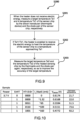
- the heater 210 of the sensing chip 202 is a current source circuit designed with an MOSFET circuit and implemented in the form of multiple current source circuits connected in parallel to increase the electrical energy P, and setting different switching in current source circuit by using current instruction HT ⁇ 3:0> in order to achieve the purpose of heating the semiconductor substrate of the sensing chip 202.
- Power denotes the operating voltage provided to the heater
- EnHT denotes an enabling signal of the heater
- HT ⁇ 3:0> denotes 4-bit configuration current instructions
- I_Vbat5(mA) denotes the current actually measured with an ammeter
- V_DIODE(V) denotes the voltage actually measured with a built-in diode temperature sensor.
- the calculated temperature is the temperature of sensing chip samples #1, #2, as calculated by substituting V_DIODE into a look-up table. Therefore, the heating temperature test results shown in FIG. 10 and FIG. 11 indicate the following:
- the heater operating at an operating voltage is effective in heating up the semiconductor substrate of the sensing chip 202 with the calculated temperature obtained with the built-in diode temperature sensor of the sensing chip 202, as the current increases.
- the sensing chip is advantageously characterized by the integration of a silicon transducer and a heater onto a semiconductor substrate to allow the silicon transducer operating at a fixed temperature after heating and thereby exhibit stable transducing characteristics.
- the heating circuit of the measuring chip provides an electrical energy to the heater of the sensing chip for raising the temperature of the semiconductor substrate, so that the silicon transducer performs temperature measurement at a temperature which approximates to a target temperature or at a predetermined temperature configured by the system.
- the silicon transducer is exemplified by a thermopile device.
- the present disclosure provides a technical solution as follows: The ambient temperature is raised such that the thermopile device starts measuring an output voltage of the thermopile device only after approaching a target temperature or only at a predetermined temperature, so that a nonlinear relation between the output voltage and the measured target temperature approaches a linear relation, render it easy for the temperature measurement system to calibrate the measured target temperature, and thus greatly enhance the accuracy of the measurement results.
- the technical solution provided by the present disclosure is further advantageous in that the measurement of the output voltage of the thermopile device begins only after the sensing chip is heated to approach the target temperature to be measured, so as the voltage signals generated by the thermopile device is diminished. When the temperature measurement system substitutes the voltage signals into a look-up table to calculate the temperature, the error of the temperature measurement is also reduced and temperature accuracy is enhanced.
- the operation of the thermopile device is enabled only after the sensing chip is heated to approach the target temperature to be measured, so as to reduce the effect of the nonlinear relation of the thermopile device associated with the temperature of the sensing chip, and calibrate a built-in heat sensor with the measuring chip for measuring the temperature of the sensing chip accurately. Therefore, the temperature measurement system requires a temperature difference measurement circuit and is able to accurately measure the difference between the temperature of the sensing chip and the temperature of the measuring chip without performing any calibration, so as to further enhance the accuracy of the measurement results of the target temperature calculated with the temperature measurement system.
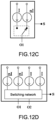
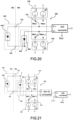
- FIG. 12A shows a multiple current source that comprises four current sources and four outputs, with the four outputs O1, O2, O3, O4 providing equal or different currents I, nI.
- the multiple current source shown in FIG. 12B comprises one current source and two outputs, with the equal current I being selectively provided at the two outputs O1, O2 according to a selection signal S.
- the multiple current source shown in FIG. 12C comprises two current sources and one output, allowing the output O1 to selectively provide two different currents I, nI according to the selection signal S.
- the multiple current source shown in FIG. 12D comprises four current sources and two outputs, allowing the two outputs O1, O2 to selectively provide equal or different currents I, nI according to the selection signal S.
- the measuring chip 304 is electrically connected to a sensing chip 302 to establish a first loop 340, wherein the sensing chip 302 is referred to as the first chip, the measuring chip 304 is referred to as the second chip.
- the measuring chip 304 comprises a second loop 350, a first multiple current source 310 and a second multiple current source 320, wherein the second loop 350 is electrically connected to at least one second diode or second diode pair 360 and the second multiple current source 320, so as to generate second voltage signals Vbe1_c, Vben_c associated with the temperature Tc of the measuring chip 304.
- the first loop 340 is electrically connected to at least one first diode or first diode pair 330 of the sensing chip 302 and the first multiple current source 310, so as to generate first voltage signals Vbe1, Vben associated with the temperature T of the sensing chip 302.
- the temperature difference calculation unit 370 performs computation on the voltage signals Vbe1, Vben, Vbe1_c, Vben_c to obtain the temperature difference associated with the temperature T of the sensing chip 302 and the temperature Tc of the measuring chip 304.
- the first diode pair 330 of the sensing chip 302 is a first PN junction element formed on a semiconductor substrate by a semiconductor manufacturing process
- the second diode pair 360 of the measuring chip 304 is a second PN junction element formed on a semiconductor substrate by a semiconductor manufacturing process.
- a temperature measurement system 300 comprises a sensing chip 302 referred to as the first chip and a measuring chip 304 referred to as the second chip.
- the measuring chip 304 is electrically connected to the sensing chip 302 via two component nodes 231, 232 and a common node 233 to establish a first loop 340.
- the sensing chip 302 comprises a first diode pair 330 electrically connected to the two component nodes 231, 232 and the common node 233.
- the first diode pair 330 is configured for sensing the temperature of the sensing chip 302 and has a junction area ratio of 1:n.
- the measuring chip 304 comprises a second loop 350, a second diode pair 360, a first multiple current source 310 and a second multiple current source 320, wherein the second diode pair 360 is configured for sensing the temperature of the measuring chip 304 and has a junction area ratio of 1:n.
- the first multiple current source 310 and the second multiple current source 320 comprise two current sources and provide two outputs with equal current values I, respectively.
- the second diode pair 360 and the common node 233 have the same reference potential.
- the first loop 340 is electrically connected to the first diode pair 330 of the sensing chip 302 and the first multiple current source 310 such that the first multiple current source 310 provides equal current values to the first diode pair 330 having a junction area ratio of 1:n for generating first voltage signals Vbe1, Vben associated with the temperature of the sensing chip 302.
- the second loop 350 is electrically connected to the second multiple current source 320 and the second diode pair 360, so that the second multiple current source 320 provide equal current values to the second diode pair 360 having a junction area ratio of 1:n for generating second voltage signals Vbe1_c, Vben_c associated with the temperature of the measuring chip 304.
- the temperature difference associated with the temperature of the sensing chip 302 and the temperature of the measuring chip 304 is calculated according to the first voltage signals Vbe1, Vben and the second voltage signals Vbe1_c, Vben_c.
- the temperature difference measurement circuit senses the temperature difference between two chips with a diode pair having equal junction areas and comprises a multiple current source in another aspect.
- the present disclosure provides a temperature measurement system 300 that comprises a sensing chip 302 referred to as the first chip and a measuring chip 304 referred to as the second chip, wherein the measuring chip 304 is electrically connected to the sensing chip 302 through the two component nodes 231, 232 and the common node 233 to establish a first loop 340.
- the sensing chip 302 comprises a first diode pair 330 electrically connected to the two component nodes 231, 232 and the common node 233, the first diode pair 330 is configured for sensing the temperature of the sensing chip 302, and has a junction area ratio of 1:1, i.e. a junction area of one diode of the first diode pair 330 is equal to a junction area of another one diode of the first diode pair 330.
- the measuring chip 304 comprises a second loop 350, a second diode pair 360, a first multiple current source 310 and a second multiple current source 320, Wherein the second diode pair 360 is configured for sensing the temperature of the measuring chip 304, and has a junction area ratio of 1:1.
- the first multiple current source 310 and the second multiple current source 320 each comprise two current sources and provide two outputs with a current ratio of 1:n. Furthermore, the second diode pair 360 and the common node 233 have the same reference potential.
- the first loop 340 is electrically connected to the first multiple current source 310 and the first diode pair 330 of the sensing chip 302 such that the first multiple current source 310 provides multiple currents with a current ratio of 1:n to the first diode pair 330 having equal junction areas for generating the first voltage signals Vbe1, Vben associated with the temperature of the sensing chip 302.
- the second loop 350 is electrically connected to the second multiple current source 320 and the second diode pair 360 such that the second multiple current source 320 provides multiple currents with a current ratio of 1:n to the second diode pair 360 with equal junction areas to generate the second voltage signals Vbe1_c, Vben_c associated with the temperature of the measuring chip 304.
- the difference between the temperature of the sensing chip 302 and the temperature of the measuring chip 304 is calculated according to the first voltage signals Vbe1, Vben and the second voltage signals Vbe1_c, Vben_c.
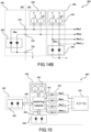
- a temperature measurement system 400 comprises a measuring chip 404 electrically connected to a sensing chip 402 to establish a first loop 440,wherein the sensing chip 402 is referred to as the first chip, the measuring chip 404 is referred to as the second chip.
- the sensing chip 402 is referred to as the first chip
- the measuring chip 404 is referred to as the second chip.
- the measuring chip 404 comprises a switching network 412 electrically connected to a plurality of sample and hold circuits 420 (S/H circuits), a multiple current source 410 and a second loop 450,wherein the second loop 450 is electrically connected to at least one second diode or second diode pair 460,and the first loop 440 is electrically connected to at least one first diode of the sensing chip 402 or the first diode pair 430.
- S/H circuits sample and hold circuits
- second loop 450 is electrically connected to at least one second diode or second diode pair 460
- the first loop 440 is electrically connected to at least one first diode of the sensing chip 402 or the first diode pair 430.
- the switching network 412 selectively switches according to a selection signal to provide the multiple current source 410 electrically connected to the first loop 440 and the second loop 450, so as to sample and retain the first voltage signals Vbe1, Vben and the second voltage signals Vbe1_c, Vben_c on the first loop 440 and the second loop 450, respectively.
- the difference between the temperature of the sensing chip 402 and the temperature of the measuring chip 404 is calculated with a temperature difference calculation unit 470 according to the voltage signals Vbe1, Vben, Vbe1_c, Vben_c.
- the first diode pair 430 of the sensing chip 402 is a first PN junction element formed on a semiconductor substrate by a semiconductor manufacturing process
- the second diode pair 460 of the measuring chip 404 is a second PN junction element formed on a semiconductor substrate by a semiconductor manufacturing process.
- the switching network 412 selectively switches to allow the multiple current source 410 to be electrically connected to the first loop 440 and the second loop 450
- the temperature difference measurement circuit senses the temperature difference between two chips based on a diode pair having a junction area ratio of 1:n, and comprises a multiple current source in an aspect.
- the temperature measurement system 400 comprises the sensing chip 402 referred to as the first chip and the measuring chip 404 referred to as the second chip, wherein the measuring chip 404 is electrically connected to the sensing chip 402 through the two component nodes 231, 232 and the common node 233 to establish a first loop 440.
- the sensing chip 402 comprises a first diode pair 430 electrically connected to the two component nodes 231, 232 and the common node 233.
- the first diode pair 430 is configured for sensing the temperature of the sensing chip 402 and has a junction area ratio of 1:n.
- the measuring chip 404 comprises a second loop 450, a second diode pair 460, and a multiple current source 410 having the switching network 412, wherein the second diode pair 460 is configured for sensing the temperature of the measuring chip 404 and has a junction area ratio of 1:n.
- the multiple current source 410 comprises two current sources I and the switching network 412 and selectively switches to provide the equal current values I to the four outputs. Furthermore, the second diode pair 460 and the common node 233 have the same reference potential.
- the switching network 412 selectively switches to allow two current sources I of the multiple current source 410 to be electrically connected to the first loop 440 and the second loop 450, respectively
- the first loop 440 is electrically connected to one of the current sources I of the multiple current source 410 and the first diode 430 of the sensing chip 402
- the second loop 450 is electrically connected to the other current source I of the multiple current source 410 and the second diode 460 of the measuring chip 404;
- the multiple current source 410 provides equal current values I to the first and second diodes 430, 460
- the sample and hold circuits 420 sample and retain the first and second voltage signals Vbe1, Vbe1_c associated with the temperature of the sensing chip 402 and the temperature of the measuring chip 404.
- the multiple current source 410 switches twice to be electrically connected to the first loop 440 and the second loop 450 and undergoes sampling and retention twice so as to obtain the first voltage signals Vbe1, Vben and the second voltage signals Vbe1_c, Vben_c, and thereby calculate the difference between the temperature of the sensing chip 402 and the temperature of the measuring chip 404.
- the first and second loops 440, 450 sample and retain the first voltage signals Vbe1, Vben associated with the temperature of the sensing chip 302, respectively, and sample and retain the two voltage signals Vbe1_c, Vben_c associated with the temperature of the measuring chip 304, respectively, and thereby calculate the difference between the temperature of the sensing chip 302 and the temperature of the measuring chip 304.
- a temperature difference measurement circuit 300 shown in FIG. 13 measures and generates the first and second voltage signals Vbe1, Vben, Vbe1_c, Vben_c at the first and second loops 340, 350, respectively, and inputs the voltage signals to the temperature difference calculation unit 370.
- the temperature difference calculation unit 370 comprises two amplifiers 371, 372 and an A/D converter 373.
- the digital signals ⁇ V BE , ⁇ V BE_C are received by an MCU.
- At least one electric power circuit of the second chip provides an electrical energy with an electrical energy ratio of 1:n in the first loop and the second loop, generates a plurality of first and second voltage signals associated with the temperature of the first chip and the temperature of the second chip corresponding to the first PN junction element and the second PN junction element, and calculates the temperature difference between the first chip and the second chip according to the plurality of first and second voltage signals.
- the first chip comprises a pair of first PN junction elements.
- the pair of first PN junction elements have a junction area ratio of 1:n.
- the second chip comprises a pair of second PN junction elements.
- the pair of second PN junction elements have a junction area ratio of 1:n.
- the present disclosure provides a temperature measurement method comprising the steps of: electrically connecting a first chip (i.e., the sensing chip) and a second chip (i.e., the measuring chip) to establish a first loop, wherein the first chip comprises at least one first PN junction element in the first loop, and the first PN junction element is used for sensing the temperature of the first chip; providing a second loop at the second chip, wherein the second chip comprises at least one second PN junction element in the second loop, and the second PN junction element is used for sensing the temperature of the second chip; providing at the second chip an electrical energy to the first loop and the second loop so as to generate a plurality of first voltage signals associated with the first PN junction element and generate a plurality of second voltage signals associated with the second PN junction element; and calculating the temperature difference between the first chip and the second chip according to the plurality of first voltage signals of the first PN junction element and the second PN junction element.
- the temperature measurement method further comprises the steps of: providing multiple currents at the second chip to flow through the first loop for providing an electrical energy to the first loop, to generate a plurality of first voltage signals associated with the first PN junction element; and providing multiple currents at the second chip to flow through the second loop for providing an electrical energy to the second loop, to generate the plurality of second voltage signals associated with the second PN junction element.
- the second chip further comprises a switching network for selectively switching multiple currents to the first loop and the second loop according to a selection signal for providing an electrical energy required for generating the plurality of first voltage signals associated with the first PN junction element and generating the plurality of second voltage signals associated with the second PN junction element and for sampling and retaining the plurality of first voltage signals and the plurality of second voltage signals according to the selection signal.
- the present disclosure provides a method of manufacturing a measuring chip, comprising the steps of: forming at least one component node and a common node on a semiconductor substrate by a semiconductor manufacturing process, wherein the component node and the common node are used for electrically connecting to at least one first PN junction element of a sensing chip; forming at least one second PN junction element on the semiconductor substrate by the semiconductor manufacturing process; and forming at least one electric power circuit on the semiconductor substrate by the semiconductor manufacturing process, wherein the at least one electric power circuit is used for providing an electrical energy to the second PN junction element and to, via the component node and the common node, the first PN junction element to generate the plurality of first voltage signals associated with the first PN junction element and generate the plurality of second voltage signals associated with the second PN junction element, wherein the plurality of first voltage signals of the first PN junction element and the plurality of second voltage signals of the second PN junction element are used for calculating and obtaining the temperature difference between the sensing
- the measuring chip 404 is electrically connected to the sensing chip 402 through the component nodes 232 and the common node 233 to establish a first loop 440, and the first loop 440 comprises the first diode 430 of the sensing chip 402.
- the measuring chip 404 comprises a second loop 450 electrically connected to a built-in second diode 460.
- the N-terminal of the first diode 430 and the N-terminal of the built-in second diode 460 of the measuring chip 404 are electrically connected to the common node 233.
- the common node 233 is connected to a reference voltage.
- the measuring chip 404 selectively switches according to a selection signal to provide current ratio with an electrical energy ratio 1:n to the first loop 440 so as to generate a plurality of first voltage signals Vbe1, Vben associated with the temperature of the sensing chip 402. Meanwhile, the measuring chip 404 selectively switches for providing multiple currents with a current ratio of 1:n to the second loop 450 according to the selection signal, so as to generate a plurality of second voltage signals Vbe1_c, Vben_c associated with the temperature of the measuring chip 404.
- the multiple currents with a current ratio of 1:n include a current source I and a current source nI.
- the two input terminals of the amplifier 472 with gain G 4 have the built-in sample and hold circuits 420 shown in FIG. 16C .
- One of the input terminals of the amplifier 472 receives the plurality of first voltage signals Vbe1, Vben.
- the other input terminal receives the plurality of second voltage signals Vbe1_c, Vben_c.
- the temperature difference measurement circuit shown in FIG. 18 has to undergo the measurement operation twice.
- the first measurement operation carried out according to the selection signal involves switching the first loop 440 and second loop 450 to the current source I, so that the input voltage of the amplifier 472 receives V be 1 - V be 1_C and the A/D converter 473 receives output voltage from the amplifier 472 and transmit the converted value to an MCU.
- the second measurement operation carried out according to the selection signal involves switching the first loop 440 and second loop 450 to the current source nI, so that the input voltage of the amplifier 472 receives V be n - V be n _C , and the A/D converter 473 receives output voltage from the amplifier 472 and transmits the converted value to the MCU.
- the MCU subtracts the A/D converted values obtained in the two measurement operations, and the result is proportional to ⁇ V BE - ⁇ V BE_C , which is equivalent to being proportional to T - T C , so as to obtain the difference between the temperature T of the sensing chip 402 and the temperature T C of the measuring chip 404.
- the input terminal signals of the amplifier 472 are diminished and the gain G 4 of the amplifier can be increased, so as to narrow down the temperature measurement range and enhance measurement accuracy.
- the gain of the amplifier to adjust the gain of the amplifier to achieve a dynamic measured temperature range with a deviation of ⁇ T, and thus the temperature measurement range is expressed as T C - ⁇ T ⁇ T C + ⁇ T, as indicated by the temperature measurement range depicted in the schematic view of FIG. 19 .
- the measurement range depicted in the circuit block diagram of FIG. 18 is flexible by adjusting the amplification ratio G 4 for different measurement ranges, so as to achieve the required temperature range. Furthermore, it is easy for the diode 430 or first PN junction element to be integrated together with the silicon transducer (exemplified by a thermopile device) onto a sensing chip 402. The diode 430 senses the ambient temperature of the thermopile device and is used for sensing the temperature difference between the sensing chip 402 and the measuring chip 404.
- the temperature difference measurement circuit can achieve an accuracy allowance of 0.01°
- the mathematical expression for the measurement of ⁇ V BE - ⁇ V B E_ C with the A/D converter is as follows:
- ADC n V ben ⁇ V ben _ C ⁇ G 4 V ref
- ADC 1 V be 1 ⁇ V be 1 _ C ⁇ G 4 V ref
- ADC n ADC n ⁇
- ADC 1 V ben ⁇ V be 1 ⁇ V ben _ C ⁇ V be 1 _ C ⁇ G 4
- V ref ⁇ V BE ⁇ ⁇ V B E _ C ⁇ G 4
- V ref K cal 4 ⁇ T ⁇ T C
- FIG. 20 and FIG. 21 there are shown an equivalent circuit diagram and another equivalent circuit diagram of the temperature difference measurement circuit shown in FIG. 18 , respectively.
- currents I, nI i.e., an electric power ratio of 1:n
- the N-terminal of the first diode 430 and the N-terminal of the second diode 460 are connected electrically and connected to a reference voltage.
- a built-in sample and hold circuit is provided at the two input terminals of the A/D converter to sample and retain the first and second voltage signals.
- the P-terminal of the first diode 430 and the P-terminal of the second diode 460 are connected electrically and connected to a reference voltage, whereas currents I, nI (i.e., an electric power ratio of 1:n) selectively flow through the N-terminal of the first diode 430 and the N-terminal of the second diode 460, respectively.
- the two input terminals of the amplifier can built-in a sample and hold circuit, so as to sample and retain the first and second voltage signals.
- the circuits shown in FIG. 20 and FIG. 21 are equivalent circuits capable of performing the same function and measuring ⁇ V BE , ⁇ V BE_C .
- a conventional semiconductor manufacturing process usually entails manufacturing a diode equivalent circuit with a P terminal - N terminal junction (P-N junction) of an element circuit.
- P-N junction P terminal - N terminal junction
- a diode exists between the base and the emitter of a transistor in a BJT (bipolar junction transistor) circuit used in a semiconductor manufacturing process.
- the equivalent circuit of a diode can be manufactured with a transistor circuit; for example, the bases of an NPN transistor and a PNP transistor serve as the common node of two diodes, whereas the emitter and the collector serve as the other nodes of the two diodes, respectively.
- the equivalent circuit of a diode can be manufactured with P-N junction elements in the other components and circuits in a semiconductor manufacturing process.
- the diodes arranged at the sensing chip and measuring chip measure the temperature difference between two chips, respectively.
- a temperature difference of 30°C and an accuracy allowance of 0.01°C only require 3000 count stability resolution, corresponding to A/D converter specification of 12-bit stability, which is easier for general A/D converters to achieve, and the requirements for signal noise suppression are also lenient.
- the present disclosure is effective in implementing high-accuracy temperature difference measurement circuits; by contrast, conventional temperature measurement circuits directly measure an external diode in order to calculate a target temperature and thus disadvantageously end up with overly wide temperature range and low accuracy.
- the temperature difference measurement circuit of the temperature measurement system measures the temperature difference between the diodes arranged at two chips, so as to attain a better accuracy.
- the temperature difference measurement circuit is characterized by small measurement input signals, and thus the measurement errors generated from external diode characteristic differences are small.
- a built-in diode of the measuring chip can be accurately calibrated during the stage of chip production to greatly enhance the accuracy of measurement results.
- the measurement of external diodes by conventional driving chips requires extra calibration for the measured target temperature with the external diodes after integration to a system production; as a result, the prior art makes it difficult to carry out mass production.
- the temperature difference measurement circuit, method and system of the present disclosure allows a measuring chip to carry out temperature difference measurement with an external diode but without performing any additional system calibration, so as to solve the conventional problems with mass production and enhance the accuracy of measurement results.
- a temperature measurement system 500 implemented by an ear thermometer is configured for measuring a user's body temperature.
- the temperature measurement system 500 comprises a sensing chip 502 referred to as the first chip, a measuring chip 504 referred to as the second chip, and a microprocessor 506, wherein the sensing chip 502 is electrically connected to the measuring chip 504 and comprises a thermopile device 511 and at least one first diode 521, the thermopile device 511 and the first diode 521 are integrated into a semiconductor substrate by a semiconductor manufacturing process.
- the measuring chip 504 is electrically connected to the microprocessor 506 and comprises a first temperature measurement circuit 510, a second temperature measurement circuit 520 and a third temperature measurement circuit 530.
- the first temperature measurement circuit 510 is a target temperature measurement circuit electrically connected to the thermopile device 511, so as to measure a voltage signal outputted from the thermopile device 511, wherein the voltage signal denotes the difference between target temperature Ta of an object under test and ambient temperature Tb of the thermopile device 511.
- the second temperature measurement circuit 520 is a temperature difference measurement circuit electrically connected to an external heat sensor and at least one second diode 522 inside the measuring chip 504, as shown in FIG. 13 through FIG. 16C , for measuring the difference between the external heat sensor and temperature Tc of the measuring chip 504, wherein the external heat sensor is configured for sensing ambient temperature Tb of the thermopile device 511.
- the third temperature measurement circuit 530 is a temperature measurement circuit electrically connected to at least one third diode 532 of the measuring chip 504, as shown in FIG. 6 , for measuring temperature Tc of the measuring chip 504.
- the external heat sensor is another self-contained diode component outside the package of the measuring chip 504.
- the external heat sensor is the first diode 521 inside the package of the sensing chip 502 outside the package of the measuring chip 504.
- the first diode 521 is inside the sensing chip 502 and outside the measuring chip 504, and the two chips 502, 504 are integrated to form one single component or integrated into the same package.
- the external heat sensor is exemplified by the first diode 521 of the sensing chip 502, and ambient temperature Tb of the thermopile device 511 is regarded as the temperature of the sensing chip 502.
- the microprocessor 506 is electrically connected to the first, second, and third temperature measurement circuits 510, 520, 530 to receive and store a first difference value (Ta-Tb), a second difference value (Tb-Tc) and a temperature value (Tc) in a memory, respectively, and thereby calculate the target temperature (Ta) of the object under test.
- the first diode 521 and the second diode 522 have the same configuration and are implemented in the form of one single diode, PN junction element, diode pair with a common node, or equivalent BJT transistor circuit.
- the present disclosure provides a temperature measurement system 500 comprising: at least one first PN junction element arranged at a first chip to sense the temperature Tb of the first chip, with the first chip integrating a silicon transducer and the at least one first PN junction element; at least one second PN junction element arranged at a second chip to sense the temperature Tc of the second chip; a first temperature measurement circuit 510 electrically connected to the silicon transducer to measure a first difference value (Ta-Tb) between the temperature Ta of an object under test and the temperature Tb of the first chip; a second temperature measurement circuit 520 electrically connected to the first PN junction element and the second PN junction element so as to measure a second difference value (Tb-Tc) between the temperature Tb of the first chip and the temperature Tc of the second chip; a third temperature measurement circuit 530 electrically connected to at least one third PN junction element of the second chip and arranged at the second chip, so as to measure the temperature Tc of the second chip;
- the present disclosure further provides a temperature measurement method, comprising the steps of: providing at least one first PN junction element arranged at a first chip to sense the temperature of the first chip, with the first chip integrating a silicon transducer and the at least one first PN junction element; providing at least one second PN junction element arranged at a second chip to sense the temperature of the second chip; measuring the silicon transducer to obtain a first difference value between the temperature of an object under test and the temperature of the first chip; measuring the first PN junction element and the second PN junction element to obtain a second difference value between the temperature of the first chip and the temperature of the second chip; measuring a temperature value of the second chip; and calculating the first difference value, the second difference value and the temperature value of the second chip to obtain a temperature value of the object under test.
- the present disclosure provides a sensing chip 502 comprising a silicon transducer and at least one first PN junction element, both being integrated onto a semiconductor substrate.
- the silicon transducer and the first PN junction element are used for electrically connecting to a measuring chip 504, so that the measuring chip 504 measures the difference (Ta-Tb) between the temperature Ta of an object under test and the temperature Tb of the semiconductor substrate through the silicon transducer, and the measuring chip 504 measures the difference (Tb-Tc) between the temperature Tb of the semiconductor substrate and the temperature Tc of the measuring chip through the first PN junction element.
- the present disclosure further provides a method of manufacturing a sensing chip 502, comprising the steps of: forming a silicon transducer on a semiconductor substrate by a semiconductor manufacturing process; and forming at least one PN junction element on the semiconductor substrate by the semiconductor manufacturing process, wherein, the first PN junction element is configured for electrically connecting to a measuring chip 504, so that the measuring chip 504 measures the difference between the temperature of the semiconductor substrate and the temperature of the measuring chip 504 through the first PN junction element.
- FIG. 23 there is shown a schematic view of a process flow of a temperature calculation method S300 of the present disclosure, with the temperature calculation method S300 applicable to the microprocessor 506 shown in FIG. 22 .
- the temperature calculation method S300 is applicable to the temperature measurement system 500 shown in FIG. 22 and comprises steps S301, S302, S303 and S304, all of which are executed by a plurality of program instructions of a computer program installed on the microprocessor 506.
- the microprocessor 506 reads a first difference value stored in a memory (not shown).
- the first difference value is outputted from the first temperature measurement circuit 510 and is the difference between the temperature of an object under test and the temperature of a sensing chip 502.
- a silicon transducer of the sensing chip 502 senses the difference between the temperature of the object under test and the temperature of the sensing chip 502.
- the microprocessor 506 reads a second difference value stored in the memory.
- the second difference value is outputted from the second temperature measurement circuit 520 and is the difference between the temperature of the sensing chip 502 and the temperature of a measuring chip 504.
- the measuring chip 504 is electrically connected to the sensing chip.
- the microprocessor 506 reads a temperature value of the measuring chip 504, with the temperature value stored in the memory and outputted from the third temperature measurement circuit 530.
- the microprocessor 506 calculates the sum of the first difference value, the second difference value and the temperature value to obtain a temperature value of the object under test.
- FIG. 24 there is shown a schematic view of the temperature measurement range of the temperature measurement system shown in FIG. 22 .
- the temperature measurement system 500 shown in FIG. 22 uses the diodes 521, 522 arranged at the sensing chip 502 and the measuring chip 504 to function as heat sensors for measuring the temperature difference between two chips, respectively.
- a temperature difference of 30°C and an accuracy allowance of 0.01°C only require 3000 count stability resolution, corresponding to A/D converter specification of 12-bit stability, which is easier for general A/D converters to achieve, and the requirements for signal noise suppression are also lenient.
- the present disclosure is conducive to the achievement of the high-accuracy temperature difference measurement circuit.
- Conventional temperature measurement circuits directly measure a diode outside a driving chip 120, as shown in FIG. 2A , leading to an overly wide temperature range and low accuracy.
- the present disclosure is advantageous in that the temperature difference measurement circuit measures the temperature difference between the diodes arranged at two chips, so as to attain enhanced accuracy.
- the input signal measured is smaller, the measurement error generated due to characteristic variation in the external diode also becomes smaller.
- the diode in the measurement chip 504 can be accurately calibrated in the production phase, hence significantly improving accuracy of the measurement results.
- the measurement of external diodes by conventional driving chips requires extra calibration for the measured target temperature with the external diodes after integration to a system product, which is difficult to carry out mass production.
- the present disclosure provides a temperature difference measurement circuit and method, enabling a measurement chip 540 to employ an external diode such that temperature difference measurement calibration can be performed without any additional system calibration. Thus, the problem in mass production and the pool accuracy in measurement result can be solved.
- the temperature measurement system 600 is implemented in the form of a mobile phone and used for measuring a target temperature of an object under test, such as a lithium battery.
- the temperature measurement system 600 comprises a sensing chip 602 referred to as the first chip, a measuring chip 604 referred to as the second chip, and a microprocessor 606, wherein the sensing chip 602 comprises at least one diode 621, which is used for sensing a target temperature.
- the sensing chip 602 is characterized in that at least one diode or a PN junction element is formed on a semiconductor substrate by a semiconductor manufacturing process.
- the measuring chip 604 measures the difference between a target temperature Ta (i.e., the temperature of the sensing chip 602) and the temperature Tc of the measuring chip 604 through the diode 621 of the sensing chip 602.
- the measuring chip 604 comprises a second temperature measurement circuit 620 and a third temperature measurement circuit 630.
- the second temperature measurement circuit 620 is a temperature difference measurement circuit electrically connected to the diode 621 of the sensing chip 602 and the diode 622 of the measuring chip 604, as shown in FIG. 13 through FIG. 16C , and adapted to measure the difference (Ta-Tc) (referred to as a second difference value) between the temperature Ta of the sensing chip 602 and the temperature Tc of the measuring chip 604.
- the third temperature measurement circuit 630 is a temperature measurement circuit electrically connected to another diode 632 of the measuring chip 604, as shown in FIG. 6 , for measuring the temperature Tc of the measuring chip 604.
- the microprocessor 606 is electrically connected to the second and third temperature measurement circuits 620, 630 for receiving and storing the second difference value (Ta-Tc) and the temperature value (Tc) in a memory (not shown), respectively, and thereby calculate the target temperature (Ta, that is, the temperature of the sensing chip 602).
- the diode 621 of the sensing chip 602 and the diode 622 of the measuring chip 604 have the same configuration and are implemented in the form of one single diode, PN junction element, diode pair with a common node, or equivalent BJT transistor circuit.
- the sensing chip 602 is another self-contained diode component outside the package of the measuring chip 604.
- the diode 621 is arranged inside the package of the sensing chip 602 outside the package of the measuring chip 604.
- the diode 621 is inside the sensing chip 602 outside the measuring chip 604.
- the two chips 602, 604 are integrated to form one single component or integrated into the same package.
- the temperature measurement system 700 is applicable to the Internet of things (IoT), so as to measure a target temperature.
- the temperature measurement system 700 comprises a sensing chip 702 referred to as the first chip and a measuring chip 704 referred to as the second chip.
- the sensing chip 702 comprises at least one diode 721 for sensing a target temperature.
- the sensing chip 702 comprises at least one diode or a PN junction element formed on a semiconductor substrate by a semiconductor manufacturing process.
- the measuring chip 704 is capable of performing wireless transmission and measuring the difference between a target temperature Ta (i.e., the temperature of the sensing chip 702) and the temperature Tc of the measuring chip 704 through the diode 721 of the sensing chip 702. Furthermore, the measuring chip 704 measures the temperature Tc thereof to calculate the target temperature Ta and wirelessly transmits the target temperature Ta to a central control system.
- the sensing chip 702 in the embodiment illustrated by FIG. 26 is identical to the sensing chip 602 in the embodiment illustrated by FIG. 25 .
- the measuring chip 704 comprises a second temperature measurement circuit 720, a third temperature measurement circuit 730, a microprocessor 740 and a wireless communication module 750.
- the second temperature measurement circuit 720 is a temperature difference measurement circuit electrically connected to the diode 721 of the sensing chip 702 and the diode 722 of the measuring chip 704, as shown in FIG. 13 through FIG. 16C , for measuring the difference (Ta-Tc), i.e., a second difference value, between the temperature Ta of the sensing chip 702 and the temperature Tc of the measuring chip 704.
- the third temperature measurement circuit 730 is a temperature measurement circuit electrically connected to another diode 732 of the measuring chip 704, as shown in FIG. 6 , for measuring the temperature Tc of the measuring chip 704.
- the microprocessor 740 is electrically connected to the second and third temperature measurement circuits 720, 730 to receive and store the second difference value (Ta-Tc) and the temperature value (Tc) in a memory (not shown), respectively, and thereby calculate the target temperature (Ta, i.e., the temperature of the sensing chip 702).
- the microprocessor 740 controls the wireless communication module 750 to wirelessly transmit the target temperature Ta to a central control system.
- the diode 721 of the sensing chip 702 and the diode 722 of the measuring chip 704 have the same configuration and are implemented in the form of one single diode, PN junction element, diode pair having a common node, or equivalent BJT transistor circuit.
- the sensing chip 702 is another self-contained diode component outside the package of the measuring chip 704.
- the diode 721 is arranged inside the package of the sensing chip 702 outside the package of the measuring chip 704.
- the diode 721 is inside the sensing chip 702 outside the measuring chip 704.
- the two chips 702, 704 are integrated to form one single component or integrated into the same package.
- the claimed invention provides a temperature measurement system comprising: at least one first PN junction element arranged at a first chip to sense the temperature of the first chip; at least one second PN junction element arranged at a second chip to sense the temperature of the second chip; a second temperature measurement circuit electrically connected to the first PN junction element and the second PN junction element and arranged at the second chip to measure and obtain a second difference value between the temperature of the first chip and the temperature of the second chip; a third temperature measurement circuit comprising at least one third PN junction element and arranged at the second chip to measure and obtain a temperature value of the second chip; and a microprocessor for calculating the second difference value and the temperature value of the second chip, so as to obtain a temperature value of the first chip.
- the temperature measurement system further comprises a wireless communication module controlled by the microprocessor to wirelessly transmit the temperature value of the first chip.
- the claimed invention provides a temperature measurement method comprising the steps of: providing at least one first PN junction element arranged at a first chip to sense the temperature of the first chip; providing at least one second PN junction element arranged at a second chip to sense the temperature of the second chip; measuring the first PN junction element and the second PN junction element, so as to obtain a second difference value between the temperature of the first chip and the temperature of the second chip; measuring a temperature value of the second chip; and calculating the sum of the second difference value and the temperature value of the second chip, so as to obtain a temperature value of the first chip.
- the temperature measurement method of the claimed invention further comprises the step of transmitting wirelessly data about the temperature of the first chip.
- the claimed invention provides a sensing chip comprising at least one PN junction element arranged on a semiconductor substrate.
- the PN junction element is used for electrically connecting to a measuring chip, so that the measuring chip measures the difference between the temperature of the sensing chip and the temperature of the measuring chip through the PN junction element.
- the claimed invention further provides a method of manufacturing a sensing chip, comprising the steps of: forming at least one PN junction element on a semiconductor substrate by a semiconductor manufacturing process; and electrically connecting the PN junction element to a measuring chip, so that the measuring chip measures the difference between the temperature of the sensing chip and the temperature of the measuring chip through the PN junction element.
- FIG. 27 there is shown a schematic view of a process flow of a temperature calculation method S400 of the claimed invention, wherein the temperature calculation method S400 is implemented to the temperature measurement system shown in FIG. 25 and FIG. 26 .
- the temperature calculation method S400 comprises steps S401, S402 and S403, all of which are executed by a plurality of program instructions of a computer program installed on the microprocessor.
- the microprocessor reads a second difference value stored in a memory (not shown), outputted from the second temperature measurement circuit, and being the difference between the temperature of a sensing chip and the temperature of a measuring chip.
- step S402 the microprocessor reads a temperature value stored in the memory, outputted from the third temperature measurement circuit, and being the temperature of the measuring chip.
- step S403 the microprocessor calculates the sum of the second difference value and the temperature value, so as to obtain a temperature value of the sensing chip.
- a sensing chip, measuring chip and temperature measurement system of the claimed invention can achieve sensing a target temperature by diodes, so as to attain a linear relation between a measurement result and the target temperature by a means of measuring a temperature difference, and obtain measurement results with an accuracy allowance of 0.01° when measuring the temperature difference between the temperature of the sensing chip and the temperature of the measuring chip with a temperature difference measurement circuit of the measuring chip.
- the block diagrams and/or the schematic views of process flows of the methods, systems and computer program product in the specific embodiments of the present disclosure illustrate various aspects of the present disclosure, allowing persons skilled in the art to understand that all combinations of the calculation blocks and/or the steps of the calculation methods of the present disclosure can be implemented with computer program instructions.
- the computer program instructions are provided to general-purpose computers, special-purpose computers or processors of any other programmable data processing equipment to generate various instructions and perform operations/functions specified in the block diagrams and/or the schematic views of process flows.
- the computer program instructions are stored in a computer-readable medium to give instructions to computers, other programmable data processing equipment or other apparatuses to operate in a specific way.
- the instructions stored in a computer-readable medium are indispensable to all operating subjects, including apparatuses performing the operations/functions specified in the block diagrams and/or the schematic views of process flows.
Landscapes
- Physics & Mathematics (AREA)
- General Physics & Mathematics (AREA)
- Spectroscopy & Molecular Physics (AREA)
- Chemical & Material Sciences (AREA)
- Crystallography & Structural Chemistry (AREA)
- Nonlinear Science (AREA)
- Measuring Temperature Or Quantity Of Heat (AREA)
Claims (26)
- Temperaturmesssystem (600, 700), das Folgendes umfasst:mindestens ein erstes PN-Übergangselement (621, 721), das an einem ersten Chip (602, 702) angeordnet ist, um eine Temperatur (Ta) des ersten Chips (602, 702) zu erfassen;mindestens ein zweites PN-Übergangselement (622, 722), das an einem zweiten Chip (604, 704) angeordnet ist, um eine Temperatur (Tc) des zweiten Chips (604, 704) zu erfassen;eine zweite Temperaturmessschaltung (620, 720), die elektrisch mit dem ersten PN-Übergangselement (621, 721) und dem zweiten PN-Übergangselement (622, 722) verbunden und an dem zweiten Chip (604, 704) angeordnet ist, um einen Temperaturdifferenzwert (Ta-Tc) zwischen der Temperatur (Ta) des ersten Chips (602, 702) und der Temperatur (Tc) des zweiten Chips (604, 704) zu messen;eine dritte Temperaturmessschaltung (630, 730), die mindestens ein drittes PN-Übergangselement (632, 732) umfasst und an dem zweiten Chip (604, 704) angeordnet ist, um einen Temperaturwert (Tc) des zweiten Chips (604, 704) zu messen; undeine Verarbeitungseinheit (606, 740) zum Berechnen des Temperaturdifferenzwertes (Ta-Tc) und des Temperaturwertes (Tc) des zweiten Chips (604, 704), um einen Temperaturwert (Ta) des ersten Chips (602, 702) zu erhalten.
- Temperaturmesssystem (600, 700) nach Anspruch 1, wobei das mindestens eine erste PN-Übergangselement (621, 721) ein Paar erster PN-Übergangselemente mit einem ersten gemeinsamen Knoten ist und das mindestens eine zweite PN-Übergangselement (622, 722) ein Paar zweiter PN-Übergangselemente mit einem zweiten gemeinsamen Knoten ist, wobei der erste und der zweite gemeinsame Knoten das gleiche Bezugspotential haben.
- Temperaturmesssystem (600, 700) nach Anspruch 2, wobei die zweite Temperaturmessschaltung (620, 720) mindestens eine Mehrfachstromquellenschaltung umfasst, wobei die mindestens eine Mehrfachstromquellenschaltung dafür sorgt, dass mehrere Ströme durch das Paar von ersten PN-Übergangselementen fließen, um eine Vielzahl von ersten Spannungssignalen zu erzeugen, die dem Paar von ersten PN-Übergangselementen zugeordnet sind, und dafür sorgt, dass mehrere Ströme durch das Paar von zweiten PN-Übergangselementen fließen, um eine Vielzahl von zweiten Spannungssignalen zu erzeugen, die dem Paar von zweiten PN-Übergangselementen zugeordnet sind.
- Temperaturmesssystem (600, 700) nach Anspruch 3, wobei die zweite Temperaturmessschaltung (620, 720) eine Recheneinheit zum Berechnen umfasst, um den Temperaturdifferenzwert (Ta-Tc) gemäß einer Mehrzahl von ersten Spannungssignalen des Paares von ersten PN-Übergangselementen und einer Mehrzahl von zweiten Spannungssignalen des Paares von zweiten PN-Übergangselementen zu erhalten.
- Temperaturmesssystem (600, 700) nach Anspruch 3, wobei die zweite Temperaturmessschaltung (620, 720) ein Schaltnetzwerk zum selektiven Schalten der Mehrfachstromquellenschaltung umfasst, um mehrere Ströme zum Fließen durch das Paar erster PN-Übergangselemente bereitzustellen und mehrere Ströme zum Fließen durch das Paar zweiter PN-Übergangselemente bereitzustellen.
- Temperaturmesssystem (600, 700) nach Anspruch 1, wobei das mindestens eine erste PN-Übergangselement (621, 721) eine Diode oder ein Diodenpaar zum Erfassen einer zu prüfenden Temperatur ist.
- Temperaturmesssystem (700) nach Anspruch 6, das ferner ein drahtloses Kommunikationsmodul (750) umfasst, das elektrisch mit der Verarbeitungseinheit (740) verbunden ist, wobei die Verarbeitungseinheit (740) den Temperaturwert (Ta) des ersten Chips (702) berechnet um die zu prüfende Temperatur zu erhalten, und das drahtlose Kommunikationsmodul (750) steuert, um die zu prüfende Temperatur durch drahtlose Kommunikation zu übertragen.
- Temperaturmesssystem (600, 700) nach Anspruch 1, wobei der erste Chip (602, 702) ein Sensorchip (602, 702) ist, der mindestens ein PN-Übergangselement (621, 721) umfasst, wobei der zweite Chip (604, 704) ein Messchip (604, 704) ist, der mindestens ein PN-Übergangselement (622, 722) umfasst, und wobei die zweite Messschaltung (620, 720), die elektrisch mit dem ersten PN-Übergangselement (621, 721) und dem zweiten PN-Übergangselement (622, 722) verbunden ist, so konfiguriert ist, dass sie einen Temperaturdifferenzwert (Ta-Tc) zwischen einer Temperatur (Ta) des Sensorchips (602, 702) und einer Temperatur (Tc) des Messchips (604, 704) misst.
- Temperaturmesssystem (600, 700) nach Anspruch 8, wobei das mindestens eine erste PN-Übergangselement (621, 721) eine Diode oder ein Diodenpaar mit einem gemeinsamen Knoten ist.
- Temperaturmesssystem (600, 700) nach Anspruch 8, wobeidie dritte Temperaturmessschaltung (630, 730) das mindestens eine dritte PN-Übergangselement (632, 732) umfasst und an dem Messchip (604, 704) zur Messung eines Temperaturwertes (Tc) des Messchips (604, 704) angeordnet ist,wobei der Temperaturdifferenzwert (Ta-Tc) und der Temperaturwert (Tc) des Messchips (604, 704) berechnet werden, um einen Temperaturwert (Ta) des Sensorchips (602, 702) zu erhalten.
- Temperaturmesssystem (600, 700) nach Anspruch 10, wobei das mindestens eine erste PN-Übergangselement (621, 721) ein Paar erster PN-Übergangselemente mit einem ersten gemeinsamen Knoten ist und das mindestens eine zweite PN-Übergangselement (622, 722) ein Paar zweiter PN-Übergangselemente mit einem zweiten gemeinsamen Knoten ist, wobei der erste und der zweite gemeinsame Knoten ein gleiches Bezugspotential haben.
- Temperaturmesssystem (600, 700) nach Anspruch 11, wobei die zweite Temperaturmessschaltung (620, 720) mindestens eine Mehrfachstromquellenschaltung umfasst, um mehrere Ströme bereitzustellen, die durch das Paar der ersten PN-Übergangselemente fließen, um mehrere erste Spannungssignale zu erzeugen, die dem Paar der ersten PN-Übergangselemente zugeordnet sind, und um mehrere Ströme bereitzustellen, die durch das Paar der zweiten PN-Übergangselemente fließen, um mehrere zweite Spannungssignale zu erzeugen, die dem Paar der zweiten PN-Übergangselemente zugeordnet sind.
- Temperaturmesssystem (600, 700) nach Anspruch 12, wobei die mindestens eine Mehrfachstromquellenschaltung mehrere Ströme mit einem Stromverhältnis von 1:n bereitstellt, die jeweils durch das Paar erster PN-Übergangselemente fließen, um mehrere erste Spannungssignale zu erzeugen, die dem Paar erster PN-Übergangselemente zugeordnet sind, und mehrere Ströme mit einem Stromverhältnis von 1:n, um durch das Paar der zweiten PN-Übergangselemente zu fließen, um eine Vielzahl von zweiten Spannungssignalen zu erzeugen, die dem Paar der zweiten PN-Übergangselemente zugeordnet sind, wobei das Paar der ersten PN-Übergangselemente ein Übergangsbereichsverhältnis von 1:1 hat und das Paar der zweiten PN-Übergangselemente ein Übergangsbereichsverhältnis von 1:1 hat.
- Temperaturmesssystem (600, 700) nach Anspruch 12, wobei die mindestens eine Mehrfachstromquellenschaltung dafür sorgt, dass jeweils gleiche Ströme I durch das Paar erster PN-Übergangselemente fließen, um eine Vielzahl erster Spannungssignale zu erzeugen, die dem Paar erster PN-Übergangselemente zugeordnet sind, und dafür sorgt, dass jeweils gleiche Ströme I durch das Paar zweiter PN-Übergangselemente fließen, um eine Vielzahl zweiter Spannungssignale zu erzeugen, die dem Paar zweiter PN-Übergangselemente zugeordnet sind, und das Paar erster PN-Übergangselemente ein Übergangsbereichsverhältnis von 1:n, und das Paar der zweiten PN-Übergangselemente ein Verhältnis der Übergangsbereiche von 1:n aufweist.
- Temperaturmesssystem (600, 700) nach Anspruch 12, wobei die zweite Temperaturmessschaltung (620, 720) ein Schaltnetzwerk umfasst, so dass die mindestens eine Mehrfachstromquellenschaltung selektiv schaltet, um gleiche Ströme I bereitzustellen, die jeweils durch das Paar erster PN-Übergangselemente fließen, schaltet, um eine Vielzahl von ersten Spannungssignalen zu erzeugen, die dem Paar der ersten PN-Übergangselemente zugeordnet sind, und selektiv schaltet, um gleiche Ströme I bereitzustellen, die durch das Paar der zweiten PN-Übergangselemente fließen, um eine Vielzahl von zweiten Spannungssignalen zu erzeugen, die dem Paar der zweiten PN-Übergangselemente zugeordnet sind, wobei das Paar der ersten PN-Übergangselemente ein Übergangsbereichsverhältnis von 1:n, und das Paar der zweiten PN-Übergangselemente hat ein Verhältnis der Übergangsbereiche von 1:n.
- Temperaturmesssystem (600, 700) nach Anspruch 12, wobei die zweite Temperaturmessschaltung (620, 720) eine Recheneinheit zum Berechnen umfasst, um den Temperaturdifferenzwert (Ta-Tc) gemäß einer Mehrzahl von ersten Spannungssignalen des Paares von ersten PN-Übergangselementen und einer Mehrzahl von zweiten Spannungssignalen des Paares von zweiten PN-Übergangselementen zu erhalten.
- Temperaturmesssystem (600, 700) nach Anspruch 10, wobei die Verarbeitungseinheit (606, 740) so konfiguriert ist, dass sie den Differenzwert (Ta-Tc) und den Temperaturwert (Tc) des Messchips (604, 704) berechnet, um den Temperaturwert (Ta) des Sensorchips (602, 702) zu erhalten.
- Temperaturmesssystem (700) nach Anspruch 17, das ferner ein drahtloses Kommunikationsmodul (750) umfasst, das elektrisch mit der Verarbeitungseinheit (740) verbunden ist, wobei die Verarbeitungseinheit (740) so konfiguriert ist, dass sie den Temperaturwert (Ta) des Sensorchips (702) berechnet und erhält und das drahtlose Kommunikationsmodul (750) steuert, um den Temperaturwert (Ta) durch drahtlose Kommunikation zu übertragen.
- Verfahren zur Temperaturmessung, das die folgenden Schritte umfasst:Bereitstellen mindestens eines ersten PN-Übergangselements (621, 721), das an einem ersten Chip (602, 702) angeordnet ist, um eine Temperatur (Ta) des ersten Chips (602, 702) zu erfassen;Bereitstellen mindestens eines zweiten PN-Übergangselements (622, 722), das an einem zweiten Chip (604, 704) angeordnet ist, um eine Temperatur (Tc) des zweiten Chips (604, 704) zu erfassen;Messen des ersten PN-Übergangselements und des zweiten PN-Übergangselements, um einen Temperaturdifferenzwert (Ta-Tc) zwischen der Temperatur (Ta) des ersten Chips (602, 702) und der Temperatur (Tc) des zweiten Chips (604, 704) zu erhalten;Messen eines Temperaturwertes (Tc) des zweiten Chips (604, 704); undBerechnen des Temperaturdifferenzwertes (Ta-Tc) und des Temperaturwertes (Tc) des zweiten Chips (604, 704), um einen Temperaturwert (Ta) des ersten Chips (602, 702) zu erhalten.
- Temperaturmessverfahren nach Anspruch 19, wobei das mindestens eine erste PN-Übergangselement (621, 721) ein Paar erster PN-Übergangselemente mit einem ersten gemeinsamen Knoten ist und das mindestens eine zweite PN-Übergangselement (622, 722) ein Paar zweiter PN-Übergangselemente mit einem zweiten gemeinsamen Knoten ist, wobei der erste und der zweite gemeinsame Knoten ein gleiches Bezugspotential haben.
- Temperaturmessverfahren nach Anspruch 20 umfassend ferner das Bereitstellen mehrerer Ströme, die durch das Paar erster PN-Übergangselemente fließen, um eine Vielzahl erster Spannungssignale zu erzeugen, die dem Paar erster PN-Übergangselemente zugeordnet sind, und das Bereitstellen mehrerer Ströme, die durch das Paar zweiter PN-Übergangselemente fließen, um eine Vielzahl zweiter Spannungssignale zu erzeugen, die dem Paar zweiter PN-Übergangselemente zugeordnet sind.
- Temperaturmessverfahren nach Anspruch 21, ferner umfassend: Berechnen des Temperaturdifferenzwertes (Ta-Tc) gemäß einer Vielzahl der ersten Spannungssignale des Paares erster PN-Übergangselemente und einer Vielzahl der zweiten Spannungssignale des Paares zweiter PN-Übergangselemente.
- Temperaturmessverfahren nach Anspruch 21, ferner umfassend: selektives Schalten durch ein Schaltnetzwerk, um mehrere Ströme zum Fließen durch das Paar von ersten PN-Übergangselementen bereitzustellen, und selektives Schalten durch das Schaltnetzwerk, um mehrere Ströme zum Fließen durch das Paar von zweiten PN-Übergangselementen bereitzustellen.
- Temperaturmessverfahren nach Anspruch 19, wobei das mindestens eine erste PN-Übergangselement (621, 721) eine Diode oder ein Diodenpaar zum Erfassen einer zu prüfenden Temperatur ist.
- Temperaturmessverfahren nach Anspruch 24, ferner umfassend die Berechnung, um den Temperaturwert (Ta) des ersten Chips als die zu prüfende Temperatur zu erhalten, und die Steuerung eines drahtlosen Kommunikationsmoduls (750), um die zu prüfende Temperatur durch drahtlose Kommunikation zu übertragen.
- Temperaturmessverfahren nach Anspruch 19 umfassend ferner die folgenden Schritte:Lesen (S401) eines Temperaturdifferenzwertes (Ta-Tc), der in einem Speicher gespeichert ist, wobei der Temperaturdifferenzwert (Ta-Tc) eine Differenz zwischen einer Temperatur (Ta) eines Sensorchips (602, 702) und einer Temperatur (Tc) eines Messchips (604, 704) ist;Lesen (S402) eines im Speicher gespeicherten Temperaturwertes (Tc), wobei der Temperaturwert (Tc) die Temperatur des Messchips (604, 704) ist; undBerechnen (S403) des Temperaturdifferenzwertes (Ta-Tc) und des Temperaturwertes (Tc), um einen Temperaturwert des Sensorchips (602, 702) zu erhalten.
Applications Claiming Priority (1)
| Application Number | Priority Date | Filing Date | Title |
|---|---|---|---|
| US202263426382P | 2022-11-18 | 2022-11-18 |
Publications (2)
| Publication Number | Publication Date |
|---|---|
| EP4372336A1 EP4372336A1 (de) | 2024-05-22 |
| EP4372336B1 true EP4372336B1 (de) | 2025-04-30 |
Family
ID=88839715
Family Applications (2)
| Application Number | Title | Priority Date | Filing Date |
|---|---|---|---|
| EP23210589.0A Active EP4372337B1 (de) | 2022-11-18 | 2023-11-17 | Messsystem und verfahren dafür |
| EP23210588.2A Active EP4372336B1 (de) | 2022-11-18 | 2023-11-17 | Messsystem und verfahren dafür |
Family Applications Before (1)
| Application Number | Title | Priority Date | Filing Date |
|---|---|---|---|
| EP23210589.0A Active EP4372337B1 (de) | 2022-11-18 | 2023-11-17 | Messsystem und verfahren dafür |
Country Status (4)
| Country | Link |
|---|---|
| US (2) | US20240167890A1 (de) |
| EP (2) | EP4372337B1 (de) |
| CN (2) | CN118057130A (de) |
| TW (4) | TW202509439A (de) |
Citations (3)
| Publication number | Priority date | Publication date | Assignee | Title |
|---|---|---|---|---|
| US6890097B2 (en) * | 2002-10-09 | 2005-05-10 | Nec Electronics Corporation | Temperature measuring sensor incorporated in semiconductor substrate, and semiconductor device containing such temperature measuring sensor |
| US20090207882A1 (en) * | 2008-02-18 | 2009-08-20 | Tsai-Chung Yu | Temperature Sensor Module |
| US8061894B2 (en) * | 2006-08-02 | 2011-11-22 | Renesas Electronics Corporation | Temperature detection circuit and semiconductor device |
Family Cites Families (6)
| Publication number | Priority date | Publication date | Assignee | Title |
|---|---|---|---|---|
| JP2001349787A (ja) | 2000-06-06 | 2001-12-21 | Seiko Epson Corp | 赤外線検出素子および測温計 |
| US6554470B2 (en) * | 2000-11-07 | 2003-04-29 | Maxim Integrated Products, Inc. | M-level diode junction temperature measurement method cancelling series and parallel parasitic influences |
| DE10341142A1 (de) * | 2003-09-06 | 2005-03-31 | Braun Gmbh | Verfahren und Vorrichtung zur Kompensation des thermischen Einflusses eines Temperaturgradienten im Sensorgehäuse eines Strahlungssensors auf die Meßgenauigkeit |
| TWI258008B (en) * | 2005-10-14 | 2006-07-11 | Aimtron Technology Corp | Temperature measurement circuit calibrated through shifting a conversion reference level |
| US7341374B2 (en) * | 2005-10-25 | 2008-03-11 | Aimtron Technology Corp. | Temperature measurement circuit calibrated through shifting a conversion reference level |
| CN113701900A (zh) * | 2020-05-22 | 2021-11-26 | 众智光电科技股份有限公司 | 红外线温度感测器 |
-
2023
- 2023-08-24 TW TW113137967A patent/TW202509439A/zh unknown
- 2023-08-24 TW TW113137955A patent/TW202503242A/zh unknown
- 2023-08-24 TW TW112131844A patent/TWI881436B/zh active
- 2023-08-24 TW TW112131845A patent/TWI881437B/zh active
- 2023-09-07 CN CN202311153837.5A patent/CN118057130A/zh active Pending
- 2023-09-07 CN CN202311156614.4A patent/CN118057131A/zh active Pending
- 2023-11-06 US US18/387,114 patent/US20240167890A1/en active Pending
- 2023-11-06 US US18/387,120 patent/US20240167891A1/en active Pending
- 2023-11-17 EP EP23210589.0A patent/EP4372337B1/de active Active
- 2023-11-17 EP EP23210588.2A patent/EP4372336B1/de active Active
Patent Citations (3)
| Publication number | Priority date | Publication date | Assignee | Title |
|---|---|---|---|---|
| US6890097B2 (en) * | 2002-10-09 | 2005-05-10 | Nec Electronics Corporation | Temperature measuring sensor incorporated in semiconductor substrate, and semiconductor device containing such temperature measuring sensor |
| US8061894B2 (en) * | 2006-08-02 | 2011-11-22 | Renesas Electronics Corporation | Temperature detection circuit and semiconductor device |
| US20090207882A1 (en) * | 2008-02-18 | 2009-08-20 | Tsai-Chung Yu | Temperature Sensor Module |
Also Published As
| Publication number | Publication date |
|---|---|
| CN118057131A (zh) | 2024-05-21 |
| EP4372337A1 (de) | 2024-05-22 |
| TWI881436B (zh) | 2025-04-21 |
| TW202422020A (zh) | 2024-06-01 |
| EP4372337B1 (de) | 2025-05-14 |
| TWI881437B (zh) | 2025-04-21 |
| EP4372336A1 (de) | 2024-05-22 |
| US20240167891A1 (en) | 2024-05-23 |
| TW202509439A (zh) | 2025-03-01 |
| CN118057130A (zh) | 2024-05-21 |
| TW202422021A (zh) | 2024-06-01 |
| TW202503242A (zh) | 2025-01-16 |
| US20240167890A1 (en) | 2024-05-23 |
Similar Documents
| Publication | Publication Date | Title |
|---|---|---|
| EP3109607B1 (de) | Verfahren zur tempeaturdriftkompensierung einer temperaturmessvorrichtung mit einem thermoelement | |
| US6751497B2 (en) | Infrared thermometer | |
| US8304734B2 (en) | Infrared sensor | |
| KR20130065705A (ko) | 전기 소자 | |
| US20180100774A1 (en) | Temperature sensing circuit with temperature coefficient estimation and compensation using time variable substrate heating | |
| CN113138025A (zh) | 一种红外测温设备的自动校准方法及装置 | |
| US20200049647A1 (en) | Sensor Device and Electronic Assembly | |
| Brush | Measurement of microwave power-A review of techniques used for measurement of high-frequency RF power | |
| EP1724560A1 (de) | Infrarot-Temperaturmessvorrichtung | |
| Moisello et al. | A MEMS-CMOS microsystem for contact-less temperature measurements | |
| US11519782B2 (en) | Offset nulling for optical power meters | |
| EP4372336B1 (de) | Messsystem und verfahren dafür | |
| JP3873528B2 (ja) | 放射体温計 | |
| Wang et al. | A digital thermometer with fast response and high precision | |
| CN112697281A (zh) | 用于耳温枪的测温电路、控制方法和耳温枪 | |
| Zhuo et al. | Design of Calibration System for Multi-Channel Thermostatic Metal Bath | |
| CN118783958A (zh) | 模数转换电路、芯片及电子设备 | |
| JP2001091360A (ja) | 輻射温度検出素子 | |
| Arunachalam et al. | Embedded temperature monitoring and control unit | |
| JPS6019446B2 (ja) | 放射温度計 | |
| CN111765985A (zh) | 一种基于12位adc实现高精度测温的电路及方法 | |
| CN217424568U (zh) | 红外传感器及电子设备 | |
| US20260016348A1 (en) | High-precision temperature measurement circuit capable of performing easy calibration | |
| CN118347598A (zh) | 基于集成式热电堆的测温结构及温度校正方法 | |
| CN121720605A (zh) | 一种利用热敏电阻增强测温芯片测温敏感性的方法 |
Legal Events
| Date | Code | Title | Description |
|---|---|---|---|
| PUAI | Public reference made under article 153(3) epc to a published international application that has entered the european phase |
Free format text: ORIGINAL CODE: 0009012 |
|
| STAA | Information on the status of an ep patent application or granted ep patent |
Free format text: STATUS: REQUEST FOR EXAMINATION WAS MADE |
|
| 17P | Request for examination filed |
Effective date: 20231117 |
|
| AK | Designated contracting states |
Kind code of ref document: A1 Designated state(s): AL AT BE BG CH CY CZ DE DK EE ES FI FR GB GR HR HU IE IS IT LI LT LU LV MC ME MK MT NL NO PL PT RO RS SE SI SK SM TR |
|
| RBV | Designated contracting states (corrected) |
Designated state(s): AL AT BE BG CH CY CZ DE DK EE ES FI FR GB GR HR HU IE IS IT LI LT LU LV MC ME MK MT NL NO PL PT RO RS SE SI SK SM TR |
|
| GRAP | Despatch of communication of intention to grant a patent |
Free format text: ORIGINAL CODE: EPIDOSNIGR1 |
|
| STAA | Information on the status of an ep patent application or granted ep patent |
Free format text: STATUS: GRANT OF PATENT IS INTENDED |
|
| RIC1 | Information provided on ipc code assigned before grant |
Ipc: G01J 5/14 20060101ALN20241210BHEP Ipc: G01J 5/00 20220101ALN20241210BHEP Ipc: G01K 3/08 20060101ALI20241210BHEP Ipc: G01K 7/01 20060101ALI20241210BHEP Ipc: G01K 13/20 20210101ALI20241210BHEP Ipc: G01J 5/12 20060101ALI20241210BHEP Ipc: G01J 5/06 20220101ALI20241210BHEP Ipc: G01J 5/061 20220101AFI20241210BHEP |
|
| RIC1 | Information provided on ipc code assigned before grant |
Ipc: G01J 5/14 20060101ALN20241218BHEP Ipc: G01J 5/00 20220101ALN20241218BHEP Ipc: G01K 3/08 20060101ALI20241218BHEP Ipc: G01K 7/01 20060101ALI20241218BHEP Ipc: G01K 13/20 20210101ALI20241218BHEP Ipc: G01J 5/12 20060101ALI20241218BHEP Ipc: G01J 5/06 20220101ALI20241218BHEP Ipc: G01J 5/061 20220101AFI20241218BHEP |
|
| INTG | Intention to grant announced |
Effective date: 20250114 |
|
| GRAS | Grant fee paid |
Free format text: ORIGINAL CODE: EPIDOSNIGR3 |
|
| GRAA | (expected) grant |
Free format text: ORIGINAL CODE: 0009210 |
|
| STAA | Information on the status of an ep patent application or granted ep patent |
Free format text: STATUS: THE PATENT HAS BEEN GRANTED |
|
| AK | Designated contracting states |
Kind code of ref document: B1 Designated state(s): AL AT BE BG CH CY CZ DE DK EE ES FI FR GB GR HR HU IE IS IT LI LT LU LV MC ME MK MT NL NO PL PT RO RS SE SI SK SM TR |
|
| REG | Reference to a national code |
Ref country code: CH Ref legal event code: EP Ref country code: GB Ref legal event code: FG4D |
|
| REG | Reference to a national code |
Ref country code: IE Ref legal event code: FG4D |
|
| REG | Reference to a national code |
Ref country code: DE Ref legal event code: R096 Ref document number: 602023003211 Country of ref document: DE |
|
| REG | Reference to a national code |
Ref country code: NL Ref legal event code: MP Effective date: 20250430 |
|
| REG | Reference to a national code |
Ref country code: AT Ref legal event code: MK05 Ref document number: 1790405 Country of ref document: AT Kind code of ref document: T Effective date: 20250430 |
|
| PG25 | Lapsed in a contracting state [announced via postgrant information from national office to epo] |
Ref country code: FI Free format text: LAPSE BECAUSE OF FAILURE TO SUBMIT A TRANSLATION OF THE DESCRIPTION OR TO PAY THE FEE WITHIN THE PRESCRIBED TIME-LIMIT Effective date: 20250430 Ref country code: PT Free format text: LAPSE BECAUSE OF FAILURE TO SUBMIT A TRANSLATION OF THE DESCRIPTION OR TO PAY THE FEE WITHIN THE PRESCRIBED TIME-LIMIT Effective date: 20250901 Ref country code: ES Free format text: LAPSE BECAUSE OF FAILURE TO SUBMIT A TRANSLATION OF THE DESCRIPTION OR TO PAY THE FEE WITHIN THE PRESCRIBED TIME-LIMIT Effective date: 20250430 |
|
| REG | Reference to a national code |
Ref country code: LT Ref legal event code: MG9D |
|
| PG25 | Lapsed in a contracting state [announced via postgrant information from national office to epo] |
Ref country code: NO Free format text: LAPSE BECAUSE OF FAILURE TO SUBMIT A TRANSLATION OF THE DESCRIPTION OR TO PAY THE FEE WITHIN THE PRESCRIBED TIME-LIMIT Effective date: 20250730 Ref country code: GR Free format text: LAPSE BECAUSE OF FAILURE TO SUBMIT A TRANSLATION OF THE DESCRIPTION OR TO PAY THE FEE WITHIN THE PRESCRIBED TIME-LIMIT Effective date: 20250731 |
|
| PG25 | Lapsed in a contracting state [announced via postgrant information from national office to epo] |
Ref country code: NL Free format text: LAPSE BECAUSE OF FAILURE TO SUBMIT A TRANSLATION OF THE DESCRIPTION OR TO PAY THE FEE WITHIN THE PRESCRIBED TIME-LIMIT Effective date: 20250430 Ref country code: PL Free format text: LAPSE BECAUSE OF FAILURE TO SUBMIT A TRANSLATION OF THE DESCRIPTION OR TO PAY THE FEE WITHIN THE PRESCRIBED TIME-LIMIT Effective date: 20250430 |
|
| PG25 | Lapsed in a contracting state [announced via postgrant information from national office to epo] |
Ref country code: BG Free format text: LAPSE BECAUSE OF FAILURE TO SUBMIT A TRANSLATION OF THE DESCRIPTION OR TO PAY THE FEE WITHIN THE PRESCRIBED TIME-LIMIT Effective date: 20250430 |
|
| PG25 | Lapsed in a contracting state [announced via postgrant information from national office to epo] |
Ref country code: HR Free format text: LAPSE BECAUSE OF FAILURE TO SUBMIT A TRANSLATION OF THE DESCRIPTION OR TO PAY THE FEE WITHIN THE PRESCRIBED TIME-LIMIT Effective date: 20250430 |
|
| PG25 | Lapsed in a contracting state [announced via postgrant information from national office to epo] |
Ref country code: AT Free format text: LAPSE BECAUSE OF FAILURE TO SUBMIT A TRANSLATION OF THE DESCRIPTION OR TO PAY THE FEE WITHIN THE PRESCRIBED TIME-LIMIT Effective date: 20250430 |
|
| PG25 | Lapsed in a contracting state [announced via postgrant information from national office to epo] |
Ref country code: RS Free format text: LAPSE BECAUSE OF FAILURE TO SUBMIT A TRANSLATION OF THE DESCRIPTION OR TO PAY THE FEE WITHIN THE PRESCRIBED TIME-LIMIT Effective date: 20250731 |
|
| PG25 | Lapsed in a contracting state [announced via postgrant information from national office to epo] |
Ref country code: IS Free format text: LAPSE BECAUSE OF FAILURE TO SUBMIT A TRANSLATION OF THE DESCRIPTION OR TO PAY THE FEE WITHIN THE PRESCRIBED TIME-LIMIT Effective date: 20250830 |
|
| PG25 | Lapsed in a contracting state [announced via postgrant information from national office to epo] |
Ref country code: LV Free format text: LAPSE BECAUSE OF FAILURE TO SUBMIT A TRANSLATION OF THE DESCRIPTION OR TO PAY THE FEE WITHIN THE PRESCRIBED TIME-LIMIT Effective date: 20250430 |
|
| PGFP | Annual fee paid to national office [announced via postgrant information from national office to epo] |
Ref country code: DE Payment date: 20251211 Year of fee payment: 3 |
|
| PG25 | Lapsed in a contracting state [announced via postgrant information from national office to epo] |
Ref country code: SM Free format text: LAPSE BECAUSE OF FAILURE TO SUBMIT A TRANSLATION OF THE DESCRIPTION OR TO PAY THE FEE WITHIN THE PRESCRIBED TIME-LIMIT Effective date: 20250430 Ref country code: DK Free format text: LAPSE BECAUSE OF FAILURE TO SUBMIT A TRANSLATION OF THE DESCRIPTION OR TO PAY THE FEE WITHIN THE PRESCRIBED TIME-LIMIT Effective date: 20250430 |
|
| PG25 | Lapsed in a contracting state [announced via postgrant information from national office to epo] |
Ref country code: CZ Free format text: LAPSE BECAUSE OF FAILURE TO SUBMIT A TRANSLATION OF THE DESCRIPTION OR TO PAY THE FEE WITHIN THE PRESCRIBED TIME-LIMIT Effective date: 20250430 |
|
| PG25 | Lapsed in a contracting state [announced via postgrant information from national office to epo] |
Ref country code: EE Free format text: LAPSE BECAUSE OF FAILURE TO SUBMIT A TRANSLATION OF THE DESCRIPTION OR TO PAY THE FEE WITHIN THE PRESCRIBED TIME-LIMIT Effective date: 20250430 |
|
| PG25 | Lapsed in a contracting state [announced via postgrant information from national office to epo] |
Ref country code: SK Free format text: LAPSE BECAUSE OF FAILURE TO SUBMIT A TRANSLATION OF THE DESCRIPTION OR TO PAY THE FEE WITHIN THE PRESCRIBED TIME-LIMIT Effective date: 20250430 |
|
| PG25 | Lapsed in a contracting state [announced via postgrant information from national office to epo] |
Ref country code: IT Free format text: LAPSE BECAUSE OF FAILURE TO SUBMIT A TRANSLATION OF THE DESCRIPTION OR TO PAY THE FEE WITHIN THE PRESCRIBED TIME-LIMIT Effective date: 20250430 |
|
| REG | Reference to a national code |
Ref country code: DE Ref legal event code: R097 Ref document number: 602023003211 Country of ref document: DE |
|
| PG25 | Lapsed in a contracting state [announced via postgrant information from national office to epo] |
Ref country code: RO Free format text: LAPSE BECAUSE OF FAILURE TO SUBMIT A TRANSLATION OF THE DESCRIPTION OR TO PAY THE FEE WITHIN THE PRESCRIBED TIME-LIMIT Effective date: 20250430 |
|
| PLBE | No opposition filed within time limit |
Free format text: ORIGINAL CODE: 0009261 |
|
| STAA | Information on the status of an ep patent application or granted ep patent |
Free format text: STATUS: NO OPPOSITION FILED WITHIN TIME LIMIT |
|
| REG | Reference to a national code |
Ref country code: CH Ref legal event code: L10 Free format text: ST27 STATUS EVENT CODE: U-0-0-L10-L00 (AS PROVIDED BY THE NATIONAL OFFICE) Effective date: 20260311 |
|
| 26N | No opposition filed |
Effective date: 20260202 |