EP4365958A1 - Solar cell, method for producing the same and photovoltaic module - Google Patents
Solar cell, method for producing the same and photovoltaic module Download PDFInfo
- Publication number
- EP4365958A1 EP4365958A1 EP22217146.4A EP22217146A EP4365958A1 EP 4365958 A1 EP4365958 A1 EP 4365958A1 EP 22217146 A EP22217146 A EP 22217146A EP 4365958 A1 EP4365958 A1 EP 4365958A1
- Authority
- EP
- European Patent Office
- Prior art keywords
- substrate
- recess
- plating layer
- solar cell
- recesses
- Prior art date
- Legal status (The legal status is an assumption and is not a legal conclusion. Google has not performed a legal analysis and makes no representation as to the accuracy of the status listed.)
- Pending
Links
- 238000004519 manufacturing process Methods 0.000 title claims abstract description 20
- 239000000758 substrate Substances 0.000 claims abstract description 189
- 238000007747 plating Methods 0.000 claims abstract description 164
- 238000005538 encapsulation Methods 0.000 claims description 10
- 239000010410 layer Substances 0.000 description 162
- 238000006243 chemical reaction Methods 0.000 description 26
- 230000015572 biosynthetic process Effects 0.000 description 19
- 238000010586 diagram Methods 0.000 description 14
- 239000000463 material Substances 0.000 description 13
- 238000005530 etching Methods 0.000 description 6
- 238000000034 method Methods 0.000 description 6
- 238000009713 electroplating Methods 0.000 description 5
- 239000002313 adhesive film Substances 0.000 description 4
- 238000010329 laser etching Methods 0.000 description 4
- 238000012546 transfer Methods 0.000 description 4
- 239000000969 carrier Substances 0.000 description 3
- 238000007772 electroless plating Methods 0.000 description 3
- 238000012986 modification Methods 0.000 description 3
- 230000004048 modification Effects 0.000 description 3
- 238000000992 sputter etching Methods 0.000 description 3
- RYGMFSIKBFXOCR-UHFFFAOYSA-N Copper Chemical compound [Cu] RYGMFSIKBFXOCR-UHFFFAOYSA-N 0.000 description 2
- PXHVJJICTQNCMI-UHFFFAOYSA-N Nickel Chemical compound [Ni] PXHVJJICTQNCMI-UHFFFAOYSA-N 0.000 description 2
- KDLHZDBZIXYQEI-UHFFFAOYSA-N Palladium Chemical compound [Pd] KDLHZDBZIXYQEI-UHFFFAOYSA-N 0.000 description 2
- XUIMIQQOPSSXEZ-UHFFFAOYSA-N Silicon Chemical compound [Si] XUIMIQQOPSSXEZ-UHFFFAOYSA-N 0.000 description 2
- RTAQQCXQSZGOHL-UHFFFAOYSA-N Titanium Chemical compound [Ti] RTAQQCXQSZGOHL-UHFFFAOYSA-N 0.000 description 2
- 150000001875 compounds Chemical class 0.000 description 2
- 229910052802 copper Inorganic materials 0.000 description 2
- 239000010949 copper Substances 0.000 description 2
- 239000005038 ethylene vinyl acetate Substances 0.000 description 2
- 230000031700 light absorption Effects 0.000 description 2
- 229920001200 poly(ethylene-vinyl acetate) Polymers 0.000 description 2
- -1 polyethylene octene copolymer Polymers 0.000 description 2
- 229920000139 polyethylene terephthalate Polymers 0.000 description 2
- 239000005020 polyethylene terephthalate Substances 0.000 description 2
- 239000011241 protective layer Substances 0.000 description 2
- 229910052710 silicon Inorganic materials 0.000 description 2
- 239000010703 silicon Substances 0.000 description 2
- 239000010936 titanium Substances 0.000 description 2
- 229910052719 titanium Inorganic materials 0.000 description 2
- MARUHZGHZWCEQU-UHFFFAOYSA-N 5-phenyl-2h-tetrazole Chemical compound C1=CC=CC=C1C1=NNN=N1 MARUHZGHZWCEQU-UHFFFAOYSA-N 0.000 description 1
- JBRZTFJDHDCESZ-UHFFFAOYSA-N AsGa Chemical compound [As]#[Ga] JBRZTFJDHDCESZ-UHFFFAOYSA-N 0.000 description 1
- VYZAMTAEIAYCRO-UHFFFAOYSA-N Chromium Chemical compound [Cr] VYZAMTAEIAYCRO-UHFFFAOYSA-N 0.000 description 1
- 229910001218 Gallium arsenide Inorganic materials 0.000 description 1
- ATJFFYVFTNAWJD-UHFFFAOYSA-N Tin Chemical compound [Sn] ATJFFYVFTNAWJD-UHFFFAOYSA-N 0.000 description 1
- HCHKCACWOHOZIP-UHFFFAOYSA-N Zinc Chemical compound [Zn] HCHKCACWOHOZIP-UHFFFAOYSA-N 0.000 description 1
- 229910052782 aluminium Inorganic materials 0.000 description 1
- XAGFODPZIPBFFR-UHFFFAOYSA-N aluminium Chemical compound [Al] XAGFODPZIPBFFR-UHFFFAOYSA-N 0.000 description 1
- 229910021417 amorphous silicon Inorganic materials 0.000 description 1
- 230000005540 biological transmission Effects 0.000 description 1
- 229910052804 chromium Inorganic materials 0.000 description 1
- 239000011651 chromium Substances 0.000 description 1
- 229910017052 cobalt Inorganic materials 0.000 description 1
- 239000010941 cobalt Substances 0.000 description 1
- GUTLYIVDDKVIGB-UHFFFAOYSA-N cobalt atom Chemical compound [Co] GUTLYIVDDKVIGB-UHFFFAOYSA-N 0.000 description 1
- UIPVMGDJUWUZEI-UHFFFAOYSA-N copper;selanylideneindium Chemical compound [Cu].[In]=[Se] UIPVMGDJUWUZEI-UHFFFAOYSA-N 0.000 description 1
- 239000012792 core layer Substances 0.000 description 1
- 230000007423 decrease Effects 0.000 description 1
- 238000011161 development Methods 0.000 description 1
- 229910003460 diamond Inorganic materials 0.000 description 1
- 239000010432 diamond Substances 0.000 description 1
- 239000011521 glass Substances 0.000 description 1
- PCHJSUWPFVWCPO-UHFFFAOYSA-N gold Chemical compound [Au] PCHJSUWPFVWCPO-UHFFFAOYSA-N 0.000 description 1
- 229910052737 gold Inorganic materials 0.000 description 1
- 239000010931 gold Substances 0.000 description 1
- 229910052738 indium Inorganic materials 0.000 description 1
- APFVFJFRJDLVQX-UHFFFAOYSA-N indium atom Chemical compound [In] APFVFJFRJDLVQX-UHFFFAOYSA-N 0.000 description 1
- 229910021424 microcrystalline silicon Inorganic materials 0.000 description 1
- 229910021421 monocrystalline silicon Inorganic materials 0.000 description 1
- 229910052759 nickel Inorganic materials 0.000 description 1
- 239000011368 organic material Substances 0.000 description 1
- 229910052763 palladium Inorganic materials 0.000 description 1
- 238000005240 physical vapour deposition Methods 0.000 description 1
- 239000004033 plastic Substances 0.000 description 1
- 229920003023 plastic Polymers 0.000 description 1
- 229910021420 polycrystalline silicon Inorganic materials 0.000 description 1
- 238000012827 research and development Methods 0.000 description 1
- HBMJWWWQQXIZIP-UHFFFAOYSA-N silicon carbide Chemical compound [Si+]#[C-] HBMJWWWQQXIZIP-UHFFFAOYSA-N 0.000 description 1
- 229910010271 silicon carbide Inorganic materials 0.000 description 1
- 229910052709 silver Inorganic materials 0.000 description 1
- 239000004332 silver Substances 0.000 description 1
- WFKWXMTUELFFGS-UHFFFAOYSA-N tungsten Chemical compound [W] WFKWXMTUELFFGS-UHFFFAOYSA-N 0.000 description 1
- 229910052721 tungsten Inorganic materials 0.000 description 1
- 239000010937 tungsten Substances 0.000 description 1
- 229910052725 zinc Inorganic materials 0.000 description 1
- 239000011701 zinc Substances 0.000 description 1
Images



Classifications
-
- H—ELECTRICITY
- H10—SEMICONDUCTOR DEVICES; ELECTRIC SOLID-STATE DEVICES NOT OTHERWISE PROVIDED FOR
- H10K—ORGANIC ELECTRIC SOLID-STATE DEVICES
- H10K30/00—Organic devices sensitive to infrared radiation, light, electromagnetic radiation of shorter wavelength or corpuscular radiation
- H10K30/50—Photovoltaic [PV] devices
- H10K30/57—Photovoltaic [PV] devices comprising multiple junctions, e.g. tandem PV cells
-
- H—ELECTRICITY
- H10—SEMICONDUCTOR DEVICES; ELECTRIC SOLID-STATE DEVICES NOT OTHERWISE PROVIDED FOR
- H10F—INORGANIC SEMICONDUCTOR DEVICES SENSITIVE TO INFRARED RADIATION, LIGHT, ELECTROMAGNETIC RADIATION OF SHORTER WAVELENGTH OR CORPUSCULAR RADIATION
- H10F77/00—Constructional details of devices covered by this subclass
- H10F77/20—Electrodes
- H10F77/206—Electrodes for devices having potential barriers
- H10F77/211—Electrodes for devices having potential barriers for photovoltaic cells
- H10F77/215—Geometries of grid contacts
-
- H—ELECTRICITY
- H10—SEMICONDUCTOR DEVICES; ELECTRIC SOLID-STATE DEVICES NOT OTHERWISE PROVIDED FOR
- H10F—INORGANIC SEMICONDUCTOR DEVICES SENSITIVE TO INFRARED RADIATION, LIGHT, ELECTROMAGNETIC RADIATION OF SHORTER WAVELENGTH OR CORPUSCULAR RADIATION
- H10F77/00—Constructional details of devices covered by this subclass
- H10F77/10—Semiconductor bodies
- H10F77/14—Shape of semiconductor bodies; Shapes, relative sizes or dispositions of semiconductor regions within semiconductor bodies
- H10F77/147—Shapes of bodies
-
- H—ELECTRICITY
- H10—SEMICONDUCTOR DEVICES; ELECTRIC SOLID-STATE DEVICES NOT OTHERWISE PROVIDED FOR
- H10F—INORGANIC SEMICONDUCTOR DEVICES SENSITIVE TO INFRARED RADIATION, LIGHT, ELECTROMAGNETIC RADIATION OF SHORTER WAVELENGTH OR CORPUSCULAR RADIATION
- H10F71/00—Manufacture or treatment of devices covered by this subclass
- H10F71/137—Batch treatment of the devices
-
- H—ELECTRICITY
- H10—SEMICONDUCTOR DEVICES; ELECTRIC SOLID-STATE DEVICES NOT OTHERWISE PROVIDED FOR
- H10F—INORGANIC SEMICONDUCTOR DEVICES SENSITIVE TO INFRARED RADIATION, LIGHT, ELECTROMAGNETIC RADIATION OF SHORTER WAVELENGTH OR CORPUSCULAR RADIATION
- H10F77/00—Constructional details of devices covered by this subclass
- H10F77/20—Electrodes
- H10F77/206—Electrodes for devices having potential barriers
- H10F77/211—Electrodes for devices having potential barriers for photovoltaic cells
-
- H—ELECTRICITY
- H10—SEMICONDUCTOR DEVICES; ELECTRIC SOLID-STATE DEVICES NOT OTHERWISE PROVIDED FOR
- H10K—ORGANIC ELECTRIC SOLID-STATE DEVICES
- H10K30/00—Organic devices sensitive to infrared radiation, light, electromagnetic radiation of shorter wavelength or corpuscular radiation
- H10K30/80—Constructional details
- H10K30/88—Passivation; Containers; Encapsulations
-
- H—ELECTRICITY
- H10—SEMICONDUCTOR DEVICES; ELECTRIC SOLID-STATE DEVICES NOT OTHERWISE PROVIDED FOR
- H10K—ORGANIC ELECTRIC SOLID-STATE DEVICES
- H10K77/00—Constructional details of devices covered by this subclass and not covered by groups H10K10/80, H10K30/80, H10K50/80 or H10K59/80
- H10K77/10—Substrates, e.g. flexible substrates
Definitions
- Embodiments of the present disclosure relate to the field of solar cells, and in particular to a solar cell, a method for producing the solar cell and a photovoltaic module.
- Solar cells have good photoelectric conversion capabilities. Thus, solar cells are the focus of clean energy development. In order to secure the photoelectric conversion efficiency of solar cells, the research and development of solar cells are ongoing. During the production of a solar cell, recesses are formed on a surface of a substrate and respective grid line is formed in each recess. In this way, currents generated by the solar cell can be collected and transferred to the module end through a bus bar.
- Embodiments of the present disclosure provide a solar cell, a method for producing the solar cell and a photovoltaic module, which are at least conducive to reducing open-circuit voltage loss and improving photoelectric conversion efficiency of the solar cell.
- a solar cell including: a substrate having a surface with a plurality of recess sets arranged at intervals along a first direction, each recess set of the plurality of recess sets including a plurality of recesses arranged at intervals along a second direction, and a distance d between adjacent recesses of the each recess set is greater than zero and less than 4L, L being a maximum dimension of a single recess of the plurality of recesses in the second direction; and a plurality of grid lines formed over the surface of the substrate. Each of the plurality of grid lines is formed in a region defined by a respective recess set and includes a first plating layer.
- the first plating layer includes portions formed on the surface of the substrate and extension portions extending into respective recesses of a respective recess set. Each of the extension portions is formed in a respective recess of the respective recess set and is in contact with the substrate through the recess.
- the maximum dimension of a recess of the plurality of recesses in the second direction ranges from 3 ⁇ m to 50 ⁇ m.
- the distance between adjacent recesses in the second direction is less than 200 ⁇ m.
- a maximum depth of a recess of the plurality of recesses in a direction perpendicular to the surface of the substrate is less than 1 ⁇ m.
- a shape of an orthogonal projection of a recess of the plurality of recesses on the surface of the substrate includes a circle, an ellipse or a polygon.
- each of the plurality of grid lines further includes a second plating layer formed on a surface of the first plating layer away from the substrate and a third plating layer formed on a surface of the second plating layer away from the substrate.
- a maximum thickness of the second plating layer in a direction perpendicular to the surface of the substrate is greater than a maximum thickness of the first plating layer in the direction perpendicular to the surface of the substrate and a maximum thickness of the third plating layer in the direction perpendicular to the surface of the substrate.
- a maximum thickness of the second plating layer in a direction perpendicular to the surface of the substrate ranges from 2 ⁇ m to 30 ⁇ m.
- a maximum thickness of the third plating layer in a direction perpendicular to the surface of the substrate ranges from 10 nm to 5 ⁇ m.
- a conductivity of the first plating layer is less than or equal to a conductivity of the second plating layer.
- a maximum thickness of the first plating layer in a direction perpendicular to the surface of the substrate ranges from 10 nm to 5 ⁇ m.
- the first plating layer includes two or more sub-plating layers sequentially formed in a direction perpendicular to the surface of the substrate.
- a distance between adjacent recess sets in the first direction ranges from 0.5 mm to 3 mm.
- Some embodiments of the present disclosure provide a method for producing a solar cell, including: providing a substrate; forming a plurality of recess sets arranged at intervals along a first direction on a surface of the substrate, each recess set of the plurality of recess sets includes a plurality of recesses arranged at intervals in a second direction, and a distance d between adjacent recesses in the each recess set is greater than zero and less than 4L, L being a maximum dimension of a single recess of the plurality of recesses in the second direction; and forming a plurality of grid lines over the surface of the substrate. Each of the plurality of grid lines is formed in a region defined by a respective recess set and includes a first plating layer.
- the first plating layer includes portions formed on the surface of the substrate and extension portions extending into respective recesses of a respective recess set. Each of the extension portions is formed in a respective recess of the respective recess set and is in contact with the substrate through the recess.
- the plurality of recess sets are formed by laser etching, ion etching or paste etching.
- forming the plurality of grid lines further includes forming a second plating layer on a surface of the first plating layer away from the substrate by electroplating.
- forming the plurality of grid lines further includes forming a third plating layer on a surface of the second plating layer away from the substrate by electroplating or electroless plating.
- Some embodiments of the present disclosure provide a photovoltaic module, including: at least one cell string including a plurality of solar cells as described above, the plurality of solar cells are electrically connected in sequence; at least one encapsulation layer configured to cover a surface of the at least one cell string; and at least one cover plate configured to cover a surface of the at least one encapsulation layer facing away from the at least one cell string.
- a plurality of recess sets arranged at intervals in a first direction are formed on a surface of the substrate of the solar cell, each of the plurality of recess sets includes a plurality of recesses arranged at intervals in the second direction, and a distance between adjacent recesses in the second direction is greater than 0 and is less than 4 times a maximum dimension of a recess of the plurality of recesses in the second direction.
- the plurality of recesses of each recess set form a discontinuous pattern consisted of a plurality of concave points on the surface of the substrate, such that an etched area of each recess set and a total etched area of the plurality of recess sets on the surface of the substrate can be reduced, thereby reducing an open-circuit voltage loss and improving a photoelectric conversion efficiency of the solar cell.
- the distance between adjacent recesses and the maximum dimension of a recess of the plurality of recesses in the second direction meet 0 ⁇ d ⁇ 4L.
- the first plating layer is formed in a region defined by a respective recess set on the surface of the substrate.
- the first plating layer includes portions formed on the surface of the substrate and extension portions each formed in a respective recess of a respective recess set, and each of the extension portions is in contact with the substrate through the recess.
- FIG. 1 is a structural schematic diagram of the plurality of recesses on the surface of the solar cell
- FIG. 2 is a structural schematic diagram of the plurality of grid lines on the surface of the solar cell
- FIG. 3 is a structural schematic diagram of the first plating layer.
- the solar cell includes a substrate 101 and a plurality of grid lines 104.
- a plurality of recess sets 102 arranged at intervals in a first direction are formed on a surface of the substrate 101, and each of the plurality of grid lines 104 is formed in a region defined by a respective recess set 102 and extends in a second direction on the surface of the substrate 101.
- Each of the plurality of recess sets 102 includes a plurality of recesses 103 arranged at intervals in the second direction, and 0 ⁇ d ⁇ 4L, herein d refers to a distance between adjacent recesses 103 in the second direction, and L refers to a maximum dimension of a recess 103 of the plurality of recesses in the second direction.
- Each of the plurality of grid lines 104 includes a first plating layer 105.
- the first plating layer 105 includes portions formed on the surface of the substrate 101 and extension portions 1051 each formed in a respective recess 103 of a respective recess set 102, and each of the extension portions 1051 is in contact with the substrate 101 through the recess 103.
- direction X refers to the first direction
- direction Y refers to the second direction.
- the plurality of recess sets 102 arranged at intervals in the first direction on the surface of the substrate 101 may be formed by laser etching, ion etching, paste etching or the like.
- Each of the plurality of recess sets 102 includes a plurality of recesses 103 arranged at intervals in the second direction, and the distance d between adjacent recesses 103 in the second direction is greater than 0 and is less than 4 times a maximum dimension L of a recess 103 of the plurality of recesses in the second direction.
- d may be equal to 0.5L, L, 1.5L, 2L, 3L, and so on.
- each of the plurality of recess sets 102 is provided with a plurality of recesses 103 arranged at intervals in the second direction, and the distance d between adjacent recesses 103 in the second direction is set to be greater than 0 and is less than 4 times a maximum dimension L of a recess 103 of the plurality of recesses in the second direction.
- each recess set 102 including a plurality of recesses 103 arranged at intervals can be obtained, and each recess set 102 forms a discontinuous pattern consisted of a plurality of concave points, such that a total etched area on the surface of the substrate 101 can be reduced, thereby reducing an open-circuit voltage loss and improving a photoelectric conversion efficiency of the solar cell.
- the plurality of grid lines 104 contact with the substrate 101 through the first plating layer 105.
- the first plating layer 105 includes portions formed on the surface of the substrate 101 and extension portions 1051 each contact with the substrate 101 through a respective recess 103 of a respective recess set 102.
- the first plating layer 105 includes not only the portions formed on the surface of the substrate 101, but also the extension portions 1051 contacted with the substrate 101 through the recess 103, the bonding force between the plurality of grid lines 104 and the substrate 101 can be greatly enhanced, thereby ensuring stability of the plurality of grid lines 104 arranged on the substrate 101. In this way, the problem of a reduced collection capability of currents of the solar cell due to one or more grid lines 104 becoming out of contact with the substrate 101 can be avoided, thereby securing the photoelectric conversion efficiency of the solar cell.
- the distance between adjacent recesses 103 and the maximum dimension of a recess 103 of the plurality of recesses in the second direction meet 0 ⁇ d ⁇ 4L.
- the distance between adjacent recesses 103 is set to be greater than 0, in order to avoid the problem of an increased etching damage due to overlapping adjacent recesses 103 resulted from an excessively small distance between adjacent recesses 103, and generation capability of photo-generated carriers of the solar cell can be secured.
- each of the plurality of grid lines 104 grows, in the second direction, from the plurality of recesses 103 of a respective recess set, a largest width of an obtained grid line 104 occurs at a center of a recess 103, and the width of the obtained grid line 104 decreases as being away from the center of a recess 103.
- the distance between adjacent recesses 103 is set to a value less than 4L, in order to ensure widths of segments of a grid line 104 in regions between adjacent recesses 103 to be large enough, and problem of a reduced current transferring capability of the plurality of grid lines due to excessively narrow segments of a grid line 104 in regions between adjacent recesses 103 resulted from an excessively large distance between adjacent recesses 103 can be avoid, thereby securing current transferring capability of the plurality of grid lines.
- the plurality of grid lines 104 are formed in a way that each of the plurality of grid lines 104 has no excessively narrow segment between adjacent recesses and no excessive width at each recess 103. In this way, a reduced light absorption area of the solar cell due to increased surface area occupied by the plurality of grid lines 104 on the surface of the substrate 101 can be avoided, thereby securing light absorption capability of the solar cell.
- the substrate 101 is configured to receive incoming light and generate photo-generated carriers.
- materials of the substrate 101 may be a silicon substrate, and the materials of the silicon substrate may include at least one of monocrystalline silicon, polycrystalline silicon, amorphous silicon or microcrystalline silicon.
- materials of the substrate 101 may include silicon carbide, organic material or multicomponent compound.
- the multicomponent compound may include but not limited to materials such as perovskite, gallium arsenide, cadmium telluride, copper indium selenium or the like.
- the first direction and the second direction may be perpendicular to each other or have an included angle of less than 90 degrees, for example, 60 degrees, 45 degrees, 30 degrees, etc., as long as the first direction and the second direction being different directions.
- embodiments of the present disclosure take the first direction and the second direction perpendicular to each other as examples to illustrate.
- the included angle between the first direction and the second direction may be set or adjusted according to actual needs and application scenarios, and embodiments of the present disclosure are not limited to this.
- the maximum dimension of a recess 103 of the plurality of recesses in the second direction ranges from 3 ⁇ m to 50 ⁇ m.
- the plurality of grid lines 104 contact, through the plurality of recesses 103, with the substrate 101 by means of the extension portions 1051 of the first plating layers 105.
- the contact resistance between a grid line 104 and the substrate 101 depends on cross-sectional areas of the plurality of recesses 103. The larger the cross-sectional areas of the plurality of recesses 103, the lower the resistance between the grid line 104 and the substrate 101 being in electrical contact through the extension portions 1051.
- the maximum dimension of the plurality of recesses 103 of each recess set 102 in the second direction is set to be within a range of 3 ⁇ m to 50 ⁇ m, in order to balance the contact resistance between the grid lines 104 and the substrate 101 being in electrical contact with each other and the open-circuit voltage loss of the solar cell.
- the maximum dimension of a recess 103 in the second direction is set to be 4 ⁇ m, 6 ⁇ m, 10 ⁇ m, 25 ⁇ m, 45 ⁇ m or the like.
- the maximum dimension of a recess 103 of the plurality of recesses in the second direction can be within the range of 3 ⁇ m to 50 ⁇ m, an etched area on the surface of the substrate 101 and therefore an open-circuit voltage loss of the solar cell can be reduced, thereby improving a photoelectric conversion efficiency of the solar cell. Meanwhile, in this way, the contact resistance between the extension portions 1051 of the grid lines 104 and the substrate 101 can be low as much as possible, thereby avoiding reduced current collection and transferring capabilities of the grid lines 104 due to excessive contact resistance, and avoiding a resulted reduction in efficiency of the solar cell.
- a maximum dimension of connecting lines between any two points on the edge of the recess 103 is set to be within the range of 3 ⁇ m to 50 ⁇ m.
- the distance between any two points on the edge of the laser spot is set to be within the range of 3 ⁇ m to 50 ⁇ m.
- the area of the recess 103 on the surface of the substrate 101 is limited to an area of a circle with a diameter of 3 ⁇ m to 50 ⁇ m. In this way, the contact resistance between the grid lines 104 and the substrate 101 and the open-circuit voltage loss of the solar cell can be reduced as much as possible, thereby securing the efficiency of the solar cell.
- the distance between adjacent recesses 103 in the second direction is less than 200 ⁇ m.
- a number of the plurality of recesses 103 of a recess set 102 depends on not only the maximum dimension of a recess of the plurality of recesses 103 in the second direction, but also the distance between adjacent recesses 103 in the second direction.
- An excessively large distance between adjacent recesses 103 in the second direction leads to an excessively small number of the plurality of recesses 103 of a recess set 102, thereby leading to a small etched area on the surface of the substrate 101, a relative high contact resistance between the grid lines 104 and the substrate 101, poor current collection and transferring capabilities of the grid lines 104, and a low photoelectric conversion efficiency of the solar cell.
- the distance between adjacent recesses 103 in the second direction is set to be less than 200 ⁇ m, for example, the distance between adjacent recesses 103 is set to be 3 ⁇ m, 6 ⁇ m, 12 ⁇ m, 60 ⁇ m, 120 ⁇ m or the like, depending on the maximum dimension of a recess 103. In this way, an etched area on the surface of the substrate 101 can be ensured to be large enough, thereby preventing a reduced efficiency of the solar cell due to reduced current collection and transferring capabilities of the grid lines 104.
- the distance between adjacent recesses 103 may vary or be fixed, as long as the conditions that the distance between adjacent recesses 103 in the second direction is less than 200 ⁇ m, and is greater than 0 and less than 4 times the maximum dimension of a recess 103 of the plurality of recesses in the second direction are met. Embodiments of the present disclosure do not limit the distance between adjacent recesses 103 to fixed.
- a shape of an orthogonal projection of a recess 103 of the plurality of recesses on the surface of the substrate 101 includes a circle, an ellipse or a polygon.
- the plurality of recesses 103 are configured to receive the extension portions 1051 of the first plating layer 105 of a respective grid line 104, such that the extension portions 1051 can contact with the substrate 101 through the recess 103.
- the shape of the orthogonal projection of a recess 103 of the plurality of recesses on the surface of the substrate 101 can be set according to the material selected for producing the first plating layer 105 and the specific application scenario for the grid lines 104.
- a recess 103 of which the orthogonal projection on the surface of the substrate 101 has a shape of a circle or an ellipse and has a relatively large area may be formed, so as to maximize, through the extension portion 1051 in the recess 103, the contact area between the respective grid line 104 and the substrate 101 when the electrical contact occurs, and to reduce the contact resistance between the respective grid line 104 and the substrate 101.
- a recess 103 of which the orthogonal projection on the surface of the substrate 101 has a shape of a polygon such as a triangle or a diamond and has a relatively small area may be formed, so as to minimize the etched area on the surface of the substrate 101 and to reduce the open-circuit voltage loss of the solar cell, thereby improving the photoelectric conversion efficiency of the solar cell.
- the orthogonal projection of a recess 103 of the plurality of recesses on the surface of the substrate 101 may be adjusted according to application scenarios and needs, to form a recess 103 with different cross-sectional areas. In this way, the contact resistance between the respective grid line 104 and the substrate 101 and the open-circuit voltage loss of the solar cell can be reduced as much as possible, thereby improving the photoelectric conversion efficiency of the solar cell.
- a maximum depth of a recess 103 of the plurality of recesses in a direction perpendicular to the surface of the substrate 101 is less than 1 ⁇ m.
- a shape of an orthogonal projection of an obtained recess 103 of the plurality of recesses on the surface of the substrate 101 may be selected according to needs.
- a recess 103 having a circular shaped orthogonal projection on the surface of the substrate 101 is taken as an example.
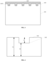
- FIG. 4 is an enlarged structural schematic diagram of a single recess 103.
- S1 refers to a maximum thickness of the substrate 101 in the direction perpendicular to the surface of the substrate 101
- S2 refers to a maximum distance between a bottom of the recess 103 and a second surface of the substrate 101 in the direction perpendicular to the surface of the substrate 101
- the second surface of the substrate 101 refers to a surface opposite to the surface of the substrate 101 on which the recess 103 is formed.
- the open-circuit voltage loss and therefore the photoelectric conversion efficiency of the solar cell are also influenced by the maximum depth of a recess 103 of the plurality of recesses in the direction perpendicular to the surface of the substrate.
- An excessive depth of the recess 103 i.e. an excessive extension distance of the recess 103 towards the interior of the substrate 101 in the direction perpendicular to the surface of the substrate 101, may lead to a relatively high open-circuit voltage loss and a reduced photoelectric conversion efficiency of the solar cell.
- the maximum depth of a recess 103 of the plurality of recesses in the direction perpendicular to the surface of the substrate 101 is set to be less than 1 ⁇ m, such as 0.1 ⁇ m, 0.15 ⁇ m, 0.3 ⁇ m, 0.5 ⁇ m, 0.85 ⁇ m, or the like. In this way, the influence on the open-circuit voltage loss of the solar cell resulted from the depth of the recess 103 can be reduced, thereby preventing the reduced photoelectric conversion efficiency of the solar cell due to excessively high open-circuit voltage loss.
- the bonding force between the first plating layer 105 and the substrate 101 can be ensured to be high enough, thereby preventing reduced current collection and transferring capabilities and reduced efficiency of the solar cell resulted from the grid lines 104 becoming out of contact with the surface of the substrate 101.
- FIG. 5 is a structural schematic diagram of a recess 103 with a dielectric film layer 106 on the plane surface of the substrate 101
- FIG. 6 is a structural schematic diagram of a recess 103 with a dielectric film layer 106 on the textured surface of the substrate 101.
- FIG. 5 is a structural schematic diagram of a recess 103 with a dielectric film layer 106 on the plane surface of the substrate 101
- FIG. 6 is a structural schematic diagram of a recess 103 with a dielectric film layer 106 on the textured surface of the substrate 101.
- the maximum depth of a recess 103 of the plurality of recesses in the direction perpendicular to the surface of the substrate 101 includes not only the extension distance of the recess 103 in the substrate 101, but also a maximum thickness of the dielectric film layer 106 crossed through by the recess 103, and it is the extension distance of the recess 103 in the substrate 101 which should not go beyond 1 ⁇ m.
- the maximum depth of a recess 103 of the plurality of recesses in the direction perpendicular to the surface of the substrate 101 may be increased appropriately depending on the maximum thickness of the dielectric film layer 106, as long as the maximum depth of the obtained recess 103 is greater than the maximum thickness of the dielectric film layer 106 and less than a sum of the maximum thickness of the dielectric film layer 106 and 1 ⁇ m.
- the recess may be formed between two adjacent bulges on the textured surface.
- the maximum depth of the recess 103 refers to a difference between a maximum distance A and a maximum distance B.
- the maximum distance A refers to a distance between a top surface of the dielectric film layer 106 on a bulge located out of a formation region of the recess 103 and a bottom surface opposite to the textured surface of the substrate 101
- the maximum distance B refers to a distance between a top surface of the etched dielectric film layer 106 on a bulge located in a formation region of the recess 103 and a bottom surface opposite to the textured surface of the substrate 101.
- etch is performed between adjacent selected bulges on the textured surface and in a direction perpendicular to the bottom of the recess 103 and directing to the interior of the substrate 101, and the maximum distance between the top surface of the dielectric film layer 106 and the bottom surface of the substrate 101 reduce, after the etch, by not more than 1 ⁇ m.
- each of the plurality of grid lines 104 further includes a second plating layer 107 formed on a surface of the first plating layer 105 away from the substrate 101 and a third plating layer 108 formed on a surface of the second plating layer 107 away from the substrate 101.
- each of the plurality of grid lines 104 is formed by the first plating layer 105, the second plating layer 107 formed on a surface of the first plating layer 105 away from the substrate 101 and the third plating layer 108 formed on a surface of the second plating layer 107 away from the substrate 101.
- the first plating layer 105 is mainly configured to fully bond with the substrate 101 through the portions formed on the surface of the substrate 101 and the extension portions 1051 each formed in a respective recess 103 and being in contact with the substrate 101, in order to improve the bonding stability between the plurality of grid lines 104 and the substrate 101.
- the second plating layer 107 is mainly configured to transfer, as a transferring center layer of a grid line 104, the collected current.
- the third plating layer 108 is mainly configured as a protective layer for the second plating layer 107 to prevent the second plating layer 107 from being damaged or broken under the condition that scrape or collision occurs, thereby securing the current collection and transferring capabilities of the plurality of grid lines 104.
- the first plating layer 105 is configured to improve the bonding stability between the plurality of grid lines 104 and the substrate 101
- the second plating layer 107 is configured to secure the current transferring capability of the grid line 104
- the third plating layer 108 is configured to improve the adaptability of the grid line 104 in practical application, reduce the possibility of fracture of the grid line 104, improve working stability of the grid line 104, and ensure the photoelectric conversion efficiency of the solar cell.
- a maximum thickness of the second plating layer 107 in the direction perpendicular to the surface of the substrate 101 is greater than a maximum thickness of the first plating layer 105 in the direction perpendicular to the surface of the substrate 101 and a maximum thickness of the third plating layer 108 in the direction perpendicular to the surface of the substrate 101.
- the second plating layer 107 is arranged between the first plating layer 105 being in contact with the substrate 101 and the third plating layer 108 functioning as a top layer, and the core function of the second plating layer 107 is to collect and transfer the current generated on the substrate 101.
- the current collection and transferring capabilities of the second plating layer 107 depend on its resistance.
- the second plating layers 107 with a same length each have a resistance depending on its cross-sectional area, and the cross-sectional area depends on the maximum thickness in the direction perpendicular to the surface of the substrate 101 and on a maximum width in a direction perpendicular to the second direction of the second plating layers 107.
- the resistance of a second plating layer 107 is negatively related to its maximum thickness in the direction perpendicular to the surface of the substrate 101.
- the maximum thickness of the second plating layer 107 is increased as much as possible, such that the maximum thickness of the second plating layer 107 is greater than the maximum thicknesses of the first plating layer 105 and the third plating layer 108.
- overall resistance of the grid line 104 can be reduced, and the current collection and transferring capabilities of the grid line 104 can be improved, thereby securing the photoelectric conversion efficiency of the solar cell.
- a maximum thickness of the second plating layer 107 in the direction perpendicular to the surface of the substrate 101 ranges from 2 ⁇ m to 30 ⁇ m.
- the core function of the second plating layer 107 is to collect and transfer the current.
- Considering the balance between an overall thickness of a grid line 104 and current collection and transferring capabilities when the maximum thickness of the second plating layer 107 in the direction perpendicular to the surface of the substrate 101 is excessively small, its small cross-sectional area leads to an excessive resistance, which prevents efficient current collection and transferring.
- the grid line 104 has an excessive overall thickness, which leads to increased production cost of the grid line 104 and an excessive weight of the solar cell.
- the maximum thickness of the second plating layer 107 in the direction perpendicular to the surface of the substrate 101 is set to be within the range of 2 ⁇ m to 30 ⁇ m, such as 3 ⁇ m, 5 ⁇ m, 8 ⁇ m, 15 ⁇ m, 25 ⁇ m, or the like.
- the second plating layer 107 is provided with a cross-sectional area large enough, in order to prevent an excessive resistance of the second plating layer 107, thereby securing the current collection and transferring capabilities of the grid line 104.
- the grid line 104 is provided with an appropriate overall thickness, thereby reducing the production cost of the grid line 104 and the weight of the solar cell.
- the maximum thickness of the second plating layer 107 in the direction perpendicular to the surface of the substrate 101 may range from 3 ⁇ m to 15 ⁇ m, such as 4 ⁇ m, 6 ⁇ m, 9 ⁇ m, 13 ⁇ m, or the like.
- the maximum thickness of the second plating layer 107 in the direction perpendicular to the surface of the substrate 101 may range from 7 ⁇ m to 20 ⁇ m, such as 8 ⁇ m, 10 ⁇ m, 13 ⁇ m, 16 ⁇ m, or the like. Embodiments of the present disclosure do not limit the maximum thickness of the second plating layer 107 in the direction perpendicular to the surface of the substrate 101 to a specific value.
- a maximum thickness of the third plating layer 108 in the direction perpendicular to the surface of the substrate 101 ranges from 10 nm to 5 ⁇ m.
- the core function of the third plating layer 108 is to function as a protective layer for the second plating layer 107, so as to prevent the second plating layer 107 from being damaged or even broken under the condition that scrape or collision occurs on the grid line 104.
- the maximum thickness of the third plating layer 108 in the direction perpendicular to the surface of the substrate 101 is set to be within the range of 10 nm to 5 ⁇ m, such as 50 nm, 150 nm, 500 nm, 1 ⁇ m, 2 ⁇ m, 4 ⁇ m, or the like.
- the grid line 104 can have an appropriate overall thickness, and the production cost of the grid line 104 and the weight of the solar cell can be reduced.
- a maximum thickness of the first plating layer 105 in the direction perpendicular to the surface of the substrate 101 ranges from 10 nm to 5 ⁇ m.
- the core function of the first plating layer 105 is to increase the bonding force between the grid line 104 and the substrate 101, thereby preventing the grid line 104 from becoming out of contact with the substrate or the occurrence of virtual open circuit when in use of the solar cell.
- the first plating layer 105 has a relatively low limit of force, which cannot effectively prevent the grid line 104 from becoming out of contact with the substrate or the occurrence of virtual open circuit when in use of the solar cell.
- the grid line 104 has an excessive overall thickness, which leads to increased production cost of the grid line 104 and an excessive weight of the solar cell.
- the maximum thickness of the first plating layer 105 in the direction perpendicular to the surface of the substrate 101 is set to be within the range of 10 nm to 5 ⁇ m, such as 100 nm, 500 nm, 1 ⁇ m, 2 ⁇ m, 4 ⁇ m, or the like.
- the grid line 104 can have an appropriate overall thickness, and the production cost of the grid line 104 and the weight of the solar cell can be reduced.
- the first plating layer 105 includes two or more sub-plating layers sequentially formed in the direction perpendicular to the surface of the substrate.
- the core function of the first plating layer 105 is to increase the bonding force between the grid line 104 and the substrate 101.
- the desired first plating layer 105 may be divided into two or more sub-plating layers in the direction perpendicular to the surface of the substrate 101, and these two or more sub-plating layers may be formed one by one to form the first plating layer 105.
- the first plating layer 105 By forming two or more sub-plating layers one by one to form the first plating layer 105, the first plating layer 105 can be formed by a plurality of stacked sub-plating layers which have more uniform structure. In this way, tightness of the structure of the first plating layer 105 can be further improved, and the limit of force of the first plating layer 105 can be increased, thereby increasing the bonding force between the grid line 104 and the substrate, and effectively preventing the grid line 104 from becoming out of contact with the substrate or the occurrence of virtual open circuit.
- a conductivity of the first plating layer 105 is less than or equal to a conductivity of the second plating layer 107.
- the core function of the first plating layer 105 is to increase the bonding force between the grid line 104 and the substrate 101, and the core function of the second plating layer 107 is to secure the current collection and transferring capabilities of the grid line 104.
- the second plating layer 107 give priority to conductivity of selected materials, and materials with relatively high conductivity are selected to form the second plating layer 107.
- a first plating layer 105 with relatively low conductivity and high bonding force with the substrate 101 and a second plating layer 107 with relatively high conductivity can be obtained.
- the bonding stability between the grid line 104 and the substrate 101 as well as the current collection and transferring capabilities of the grid line 104 can be secured, thereby securing the photoelectric conversion efficiency of the solar cell.
- a distance between adjacent recess sets 102 in the first direction ranges from 0.5 mm to 3 mm.
- Each of the plurality of grid lines 104 is formed in a region defined by a respective recess set 102.
- density of the plurality of grid lines 104 on the surface of the solar cell depends on the distance between adjacent recess sets 102. Since the plurality of grid lines 104 are configured to collect and transfer the currents generated by the solar cell, the smaller the distance between adjacent recess sets 102 in the first direction, i.e. the higher the density of the plurality of grid lines 104, the stronger the current collection and transferring capabilities of the solar cell.
- the higher the density of adj acent recess sets 102 the larger the etched area on the surface of the solar cell, the higher the open-circuit voltage loss, which leads to a reduced current generation capability of the solar cell.
- the distance between adjacent recess sets 102 is set to be within the range of 0.5 mm to 3 mm, such as 0.6 mm, 1 mm, 1.5 mm, 2 mm, 2.8 mm, or the like.
- the current collection and transferring capabilities of the solar cell can be improved by an appropriate density of the plurality of grid lines 104 on the surface of the solar cell, and the solar cell can have an appropriate open-circuit voltage loss, thereby preventing from influencing the current generation capability and photoelectric conversion efficiency of the solar cell.
- each of the plurality of recess sets 102 includes a plurality of recesses 103 arranged at intervals in the second direction, and the distance between adjacent recesses 103 in the second direction is greater than 0 and is less than 4 times the maximum dimension of a recess 103 of the plurality of recesses in the second direction.
- the plurality of recesses of each recess set 102 form a discontinuous pattern consisted of a plurality of concave points, such that an etched area on the surface of the substrate can be reduced, thereby reducing an open-circuit voltage loss and improving a photoelectric conversion efficiency of the solar cell.
- the first plating layer 105 is formed in a region defined by a respective recess set 102 on the surface of the substrate 101.
- the first plating layer 105 includes portions formed on the surface of the substrate 101 and extension portions 1051 extending into respective recesses 103 of a respective recess set 102, each of the extension portions 1051 is formed in a respective recess 103 of the respective recess set 102 and is in contact with the substrate 101 through the recess 103.
- binding force between the plurality of grid lines 104 and the substrate 101 can be improved, and reduction of the photoelectric conversion efficiency of the solar cell due to one or more grid lines 104 becoming out of contact with the substrate 101 can be avoided, thereby securing the photoelectric conversion efficiency of the solar cell.
- Embodiments of the present disclosure further provide a method for producing the solar cell as illustrated above.
- the process of the method can be seen in FIG. 8 , including operations as follows.
- each of the plurality of recess sets 102 includes a plurality of recesses 103 arranged at intervals in a second direction, and 0 ⁇ d ⁇ 4L, herein d refers to a distance between adjacent recesses 103 in the second direction, and L refers to a maximum dimension of a recess 103 of the plurality of recesses in the second direction.
- the operation of forming the plurality of recess sets 102 includes laser etching, ion etching or paste etching.
- a suitable process can be selected among the plurality of etching processes according to scenarios and needs, in order to improve the adaptability of the solution.
- each of the plurality of grid lines 104 is formed in a region defined by a respective recess set 102 and extends in the second direction.
- a first plating layer 105 is formed in the region defined by a respective recess set 102.
- the first plating layer 105 includes portions formed on the surface of the substrate 101 and extension portions 1051 extending into respective recesses 103 of a respective recess set 102, each of the extension portions 1051 is formed in a respective recess 103 of the respective recess set 102 and is in contact with the substrate 101 through the recess 103.
- a respective grid line 104 is formed based on the first plating layer 105.
- the first plating layer 105 is formed by a process of electroplating, electroless plating or physical vapor deposition.
- a suitable process can be selected among the plurality of plating layer production processes according to scenarios and needs, in order to improve the adaptability and practicability of the solution.
- the operation of forming the plurality of grid lines 104 further includes forming a second plating layer 107 on a surface of the first plating layer 105 away from the substrate 101 by electroplating.
- the operation of forming the plurality of grid lines 104 further includes forming a third plating layer 108 on a surface of the second plating layer 107 away from the substrate 101 by electroplating or electroless plating.
- the materials of the first plating layer 105 include one or more of nickel, copper, titanium, aluminum, gold, titanium, zinc, cobalt, palladium, indium, chromium and tungsten.
- the second plating layer 107 may include copper or the like, and the third plating layer 108 may include tin, silver, or the like.
- Embodiments of the present disclosure further provide a photovoltaic module, referring to FIG. 9 , the photovoltaic module includes: at least one cell string including a plurality of solar cells 110 as illustrated hereinabove, the plurality of solar cells 101 are electrically connected in sequence; at least one encapsulation layer 120 configured to cover a surface of the at least one cell string; and at least one cover plate 130 configured to cover a surface of the at least one encapsulation layer 120 facing away from the at least one cell string.
- the solar cells 110 are electrically connected in a form of a whole piece or multiple pieces to form a plurality of cell strings, and the plurality of cell strings are electrically connected in series and/or parallel.
- the plurality of cell strings may be electrically connected through conductive bars 140.
- the encapsulation layers 120 cover the front and rear surfaces of the solar cells 110.
- the encapsulation layers 120 may be an organic encapsulation adhesive film such as an ethylene vinyl acetate copolymer (EVA) adhesive film, a polyethylene octene copolymer (POE) adhesive film, or a polyethylene terephthalate (PET) adhesive film.
- EVA ethylene vinyl acetate copolymer
- POE polyethylene octene copolymer
- PET polyethylene terephthalate
- the cover plate 130 may be a glass cover plate, a plastic cover plate or the like with a light transmission function.
- a surface of the cover plate 130 facing to the encapsulation layer 120 may be a textured surface, thereby increasing the utilization of incident light.
Landscapes
- Physics & Mathematics (AREA)
- Electromagnetism (AREA)
- Photovoltaic Devices (AREA)
Abstract
Embodiments of the present disclosure relates to a solar cell, a method for producing the solar cell and a photovoltaic module. The solar cell includes a substrate having a surface with a plurality of recess sets arranged at intervals along a first direction, each recess set of the plurality of recess sets including a plurality of recesses arranged at intervals along a second direction, and a distance d between adjacent recesses of the each recess set is greater than zero and less than 4L, L being a maximum dimension of a single recess of the plurality of recesses in the second direction; and a plurality of grid lines formed over the surface of the substrate. Each of the plurality of grid lines is formed in a region defined by a respective recess set and includes a first plating layer. The first plating layer includes portions formed on the surface of the substrate and extension portions extending into respective recesses of a respective recess set. Each of the extension portions is formed in a respective recess of the respective recess set and is in contact with the substrate through the recess. Embodiments of the present disclosure are conducive to reducing open-circuit voltage loss and improving efficiency of the solar cell.
Description
- Embodiments of the present disclosure relate to the field of solar cells, and in particular to a solar cell, a method for producing the solar cell and a photovoltaic module.
- Solar cells have good photoelectric conversion capabilities. Thus, solar cells are the focus of clean energy development. In order to secure the photoelectric conversion efficiency of solar cells, the research and development of solar cells are ongoing. During the production of a solar cell, recesses are formed on a surface of a substrate and respective grid line is formed in each recess. In this way, currents generated by the solar cell can be collected and transferred to the module end through a bus bar.
- However, the existing solar cells have the problem of low photoelectric conversion efficiency.
- Embodiments of the present disclosure provide a solar cell, a method for producing the solar cell and a photovoltaic module, which are at least conducive to reducing open-circuit voltage loss and improving photoelectric conversion efficiency of the solar cell.
- Some embodiments of the present disclosure provide a solar cell, including: a substrate having a surface with a plurality of recess sets arranged at intervals along a first direction, each recess set of the plurality of recess sets including a plurality of recesses arranged at intervals along a second direction, and a distance d between adjacent recesses of the each recess set is greater than zero and less than 4L, L being a maximum dimension of a single recess of the plurality of recesses in the second direction; and a plurality of grid lines formed over the surface of the substrate. Each of the plurality of grid lines is formed in a region defined by a respective recess set and includes a first plating layer. The first plating layer includes portions formed on the surface of the substrate and extension portions extending into respective recesses of a respective recess set. Each of the extension portions is formed in a respective recess of the respective recess set and is in contact with the substrate through the recess.
- In some embodiments, the maximum dimension of a recess of the plurality of recesses in the second direction ranges from 3 µm to 50 µm.
- In some embodiments, the distance between adjacent recesses in the second direction is less than 200 µm.
- In some embodiments, a maximum depth of a recess of the plurality of recesses in a direction perpendicular to the surface of the substrate is less than 1 µm.
- In some embodiments, a shape of an orthogonal projection of a recess of the plurality of recesses on the surface of the substrate includes a circle, an ellipse or a polygon.
- In some embodiments, each of the plurality of grid lines further includes a second plating layer formed on a surface of the first plating layer away from the substrate and a third plating layer formed on a surface of the second plating layer away from the substrate.
- In some embodiments, a maximum thickness of the second plating layer in a direction perpendicular to the surface of the substrate is greater than a maximum thickness of the first plating layer in the direction perpendicular to the surface of the substrate and a maximum thickness of the third plating layer in the direction perpendicular to the surface of the substrate.
- In some embodiments, a maximum thickness of the second plating layer in a direction perpendicular to the surface of the substrate ranges from 2 µm to 30 µm.
- In some embodiments, a maximum thickness of the third plating layer in a direction perpendicular to the surface of the substrate ranges from 10 nm to 5 µm.
- In some embodiments, a conductivity of the first plating layer is less than or equal to a conductivity of the second plating layer.
- In some embodiments, a maximum thickness of the first plating layer in a direction perpendicular to the surface of the substrate ranges from 10 nm to 5 µm.
- In some embodiments, the first plating layer includes two or more sub-plating layers sequentially formed in a direction perpendicular to the surface of the substrate.
- In some embodiments, a distance between adjacent recess sets in the first direction ranges from 0.5 mm to 3 mm.
- Some embodiments of the present disclosure provide a method for producing a solar cell, including: providing a substrate; forming a plurality of recess sets arranged at intervals along a first direction on a surface of the substrate, each recess set of the plurality of recess sets includes a plurality of recesses arranged at intervals in a second direction, and a distance d between adjacent recesses in the each recess set is greater than zero and less than 4L, L being a maximum dimension of a single recess of the plurality of recesses in the second direction; and forming a plurality of grid lines over the surface of the substrate. Each of the plurality of grid lines is formed in a region defined by a respective recess set and includes a first plating layer. The first plating layer includes portions formed on the surface of the substrate and extension portions extending into respective recesses of a respective recess set. Each of the extension portions is formed in a respective recess of the respective recess set and is in contact with the substrate through the recess.
- In some embodiments, the plurality of recess sets are formed by laser etching, ion etching or paste etching.
- In some embodiments, forming the plurality of grid lines further includes forming a second plating layer on a surface of the first plating layer away from the substrate by electroplating.
- In some embodiments, forming the plurality of grid lines further includes forming a third plating layer on a surface of the second plating layer away from the substrate by electroplating or electroless plating.
- Some embodiments of the present disclosure provide a photovoltaic module, including: at least one cell string including a plurality of solar cells as described above, the plurality of solar cells are electrically connected in sequence; at least one encapsulation layer configured to cover a surface of the at least one cell string; and at least one cover plate configured to cover a surface of the at least one encapsulation layer facing away from the at least one cell string.
- One or more embodiments are exemplarily illustrated in reference to corresponding accompanying drawing(s), and these exemplary illustrations do not constitute limitations on the embodiments. Unless otherwise stated, the accompanying drawings do not constitute scale limitations.
-
FIG. 1 is a structural schematic diagram of the plurality of recesses of a solar cell according to some embodiments of the present disclosure. -
FIG. 2 is a structural schematic diagram of the plurality of grid lines of the solar cell according to some embodiments of the present disclosure. -
FIG. 3 is a structural schematic diagram of the first plating layer of the solar cell according to some embodiments of the present disclosure. -
FIG. 4 is a partially enlarged structural schematic diagram of a recess according to some embodiments of the present disclosure. -
FIG. 5 is another partially enlarged structural schematic diagram of a recess according to some embodiments of the present disclosure. -
FIG. 6 is still another partially enlarged structural schematic diagram of a recess according to some embodiments of the present disclosure. -
FIG. 7 is another structural schematic diagram of a grid line of the solar cell according to some embodiments of the present disclosure. -
FIG. 8 is a flow chart of a method for producing a solar cell according to some embodiments of the present disclosure. -
FIG. 9 is a structural schematic diagram of a photovoltaic module according to some embodiments of the present disclosure. - It can be known from the background art that the existing solar cells have a poor photoelectric conversion efficiency.
- In the solar cell provided by embodiments of the present disclosure, a plurality of recess sets arranged at intervals in a first direction are formed on a surface of the substrate of the solar cell, each of the plurality of recess sets includes a plurality of recesses arranged at intervals in the second direction, and a distance between adjacent recesses in the second direction is greater than 0 and is less than 4 times a maximum dimension of a recess of the plurality of recesses in the second direction. In this way, the plurality of recesses of each recess set form a discontinuous pattern consisted of a plurality of concave points on the surface of the substrate, such that an etched area of each recess set and a total etched area of the plurality of recess sets on the surface of the substrate can be reduced, thereby reducing an open-circuit voltage loss and improving a photoelectric conversion efficiency of the solar cell. Moreover, the distance between adjacent recesses and the maximum dimension of a recess of the plurality of recesses in the second direction meet 0 < d < 4L. In this way, problems of an increased etching damage due to overlapping recesses resulted from an excessively small distance between adjacent recesses and of a reduced current transferring capability of the plurality of grid lines due to excessively narrow segments of a grid line in regions between adjacent recesses resulted from an excessively large distance between adjacent recesses can be avoid, thereby securing generation capability of photo-generated carriers of the solar cell and current transferring capability of the plurality of grid lines. During the production of the plurality of grid lines extending in the second direction, the first plating layer is formed in a region defined by a respective recess set on the surface of the substrate. The first plating layer includes portions formed on the surface of the substrate and extension portions each formed in a respective recess of a respective recess set, and each of the extension portions is in contact with the substrate through the recess. In this way, binding force between the plurality of grid lines and the substrate can be improved, and reduction of the photoelectric conversion efficiency of the solar cell due to one or more grid lines of the solar cell becoming out of contact with the substrate can be avoided, thereby securing the photoelectric conversion efficiency of the solar cell.
- Embodiments of the present disclosure will be described in detail below with reference to the accompanying drawings. Those skilled in the art should understand that, in the embodiments of the present disclosure, many technical details are provided for the reader to better understand the present disclosure. However, even without these technical details and various modifications and variants based on the following embodiments, the technical solutions claimed in the present disclosure can be realized.
- Referring to
FIGS. 1 to 3 ,FIG. 1 is a structural schematic diagram of the plurality of recesses on the surface of the solar cell,FIG. 2 is a structural schematic diagram of the plurality of grid lines on the surface of the solar cell, andFIG. 3 is a structural schematic diagram of the first plating layer. The solar cell includes asubstrate 101 and a plurality ofgrid lines 104. A plurality of recess sets 102 arranged at intervals in a first direction are formed on a surface of thesubstrate 101, and each of the plurality ofgrid lines 104 is formed in a region defined by a respective recess set 102 and extends in a second direction on the surface of thesubstrate 101. Each of the plurality ofrecess sets 102 includes a plurality ofrecesses 103 arranged at intervals in the second direction, and 0 < d < 4L, herein d refers to a distance betweenadjacent recesses 103 in the second direction, and L refers to a maximum dimension of arecess 103 of the plurality of recesses in the second direction. Each of the plurality ofgrid lines 104 includes afirst plating layer 105. Thefirst plating layer 105 includes portions formed on the surface of thesubstrate 101 andextension portions 1051 each formed in arespective recess 103 of a respective recess set 102, and each of theextension portions 1051 is in contact with thesubstrate 101 through therecess 103. Herein, direction X refers to the first direction, and direction Y refers to the second direction. - The plurality of recess sets 102 arranged at intervals in the first direction on the surface of the
substrate 101 may be formed by laser etching, ion etching, paste etching or the like. Each of the plurality of recess sets 102 includes a plurality ofrecesses 103 arranged at intervals in the second direction, and the distance d betweenadjacent recesses 103 in the second direction is greater than 0 and is less than 4 times a maximum dimension L of arecess 103 of the plurality of recesses in the second direction. For example, d may be equal to 0.5L, L, 1.5L, 2L, 3L, and so on. During the formation of the plurality of recess sets 102 arranged at intervals in the first direction on the surface of thesubstrate 101 of the solar cell, each of the plurality of recess sets 102 is provided with a plurality ofrecesses 103 arranged at intervals in the second direction, and the distance d betweenadjacent recesses 103 in the second direction is set to be greater than 0 and is less than 4 times a maximum dimension L of arecess 103 of the plurality of recesses in the second direction. In this way, recess sets 102 including a plurality ofrecesses 103 arranged at intervals can be obtained, and each recess set 102 forms a discontinuous pattern consisted of a plurality of concave points, such that a total etched area on the surface of thesubstrate 101 can be reduced, thereby reducing an open-circuit voltage loss and improving a photoelectric conversion efficiency of the solar cell. During the production of the plurality ofgrid lines 104 extending in the second direction, the plurality ofgrid lines 104 contact with thesubstrate 101 through thefirst plating layer 105. Thefirst plating layer 105 includes portions formed on the surface of thesubstrate 101 andextension portions 1051 each contact with thesubstrate 101 through arespective recess 103 of a respective recess set 102. Since thefirst plating layer 105 includes not only the portions formed on the surface of thesubstrate 101, but also theextension portions 1051 contacted with thesubstrate 101 through therecess 103, the bonding force between the plurality ofgrid lines 104 and thesubstrate 101 can be greatly enhanced, thereby ensuring stability of the plurality ofgrid lines 104 arranged on thesubstrate 101. In this way, the problem of a reduced collection capability of currents of the solar cell due to one ormore grid lines 104 becoming out of contact with thesubstrate 101 can be avoided, thereby securing the photoelectric conversion efficiency of the solar cell. - Moreover, the distance between
adjacent recesses 103 and the maximum dimension of arecess 103 of the plurality of recesses in the second direction meet 0 < d < 4L. The distance betweenadjacent recesses 103 is set to be greater than 0, in order to avoid the problem of an increased etching damage due to overlappingadjacent recesses 103 resulted from an excessively small distance betweenadjacent recesses 103, and generation capability of photo-generated carriers of the solar cell can be secured. Since each of the plurality ofgrid lines 104 grows, in the second direction, from the plurality ofrecesses 103 of a respective recess set, a largest width of an obtainedgrid line 104 occurs at a center of arecess 103, and the width of the obtainedgrid line 104 decreases as being away from the center of arecess 103. In view of this, the distance betweenadjacent recesses 103 is set to a value less than 4L, in order to ensure widths of segments of agrid line 104 in regions betweenadjacent recesses 103 to be large enough, and problem of a reduced current transferring capability of the plurality of grid lines due to excessively narrow segments of agrid line 104 in regions betweenadjacent recesses 103 resulted from an excessively large distance betweenadjacent recesses 103 can be avoid, thereby securing current transferring capability of the plurality of grid lines. Furthermore, the plurality ofgrid lines 104 are formed in a way that each of the plurality ofgrid lines 104 has no excessively narrow segment between adjacent recesses and no excessive width at eachrecess 103. In this way, a reduced light absorption area of the solar cell due to increased surface area occupied by the plurality ofgrid lines 104 on the surface of thesubstrate 101 can be avoided, thereby securing light absorption capability of the solar cell. - The
substrate 101 is configured to receive incoming light and generate photo-generated carriers. In some embodiments, materials of thesubstrate 101 may be a silicon substrate, and the materials of the silicon substrate may include at least one of monocrystalline silicon, polycrystalline silicon, amorphous silicon or microcrystalline silicon. In some other embodiments, materials of thesubstrate 101 may include silicon carbide, organic material or multicomponent compound. The multicomponent compound may include but not limited to materials such as perovskite, gallium arsenide, cadmium telluride, copper indium selenium or the like. - In some embodiments, the first direction and the second direction may be perpendicular to each other or have an included angle of less than 90 degrees, for example, 60 degrees, 45 degrees, 30 degrees, etc., as long as the first direction and the second direction being different directions. For the convenience of description and understanding, embodiments of the present disclosure take the first direction and the second direction perpendicular to each other as examples to illustrate. In specific applications, the included angle between the first direction and the second direction may be set or adjusted according to actual needs and application scenarios, and embodiments of the present disclosure are not limited to this.
- In some embodiments, the maximum dimension of a
recess 103 of the plurality of recesses in the second direction ranges from 3 µm to 50 µm. The plurality ofgrid lines 104 contact, through the plurality ofrecesses 103, with thesubstrate 101 by means of theextension portions 1051 of the first plating layers 105. The contact resistance between agrid line 104 and thesubstrate 101 depends on cross-sectional areas of the plurality ofrecesses 103. The larger the cross-sectional areas of the plurality ofrecesses 103, the lower the resistance between thegrid line 104 and thesubstrate 101 being in electrical contact through theextension portions 1051. However, excessively large cross-sectional areas of the plurality ofrecesses 103 lead to increased open-circuit voltage loss of the solar cell, thereby affecting the photoelectric conversion efficiency of the solar cell. When the plurality ofrecesses 103 have identical widths and depths, an excessively small maximum dimension of arecess 103 of the plurality of recesses in the second direction leads to an excessively high resistance between agrid line 104 and thesubstrate 101, thereby affecting the current collection and transferring capabilities of thegrid line 104. When arecess 103 of the plurality of recesses has an excessively large maximum dimension in the second direction, the solar cell has an excessively high open-circuit voltage loss and reduced photoelectric conversion efficiency. - In view of this, the maximum dimension of the plurality of
recesses 103 of each recess set 102 in the second direction is set to be within a range of 3 µm to 50 µm, in order to balance the contact resistance between thegrid lines 104 and thesubstrate 101 being in electrical contact with each other and the open-circuit voltage loss of the solar cell. For example, the maximum dimension of arecess 103 in the second direction is set to be 4 µm, 6 µm, 10 µm, 25 µm, 45 µm or the like. By setting the maximum dimension of arecess 103 of the plurality of recesses in the second direction to be within the range of 3 µm to 50 µm, an etched area on the surface of thesubstrate 101 and therefore an open-circuit voltage loss of the solar cell can be reduced, thereby improving a photoelectric conversion efficiency of the solar cell. Meanwhile, in this way, the contact resistance between theextension portions 1051 of thegrid lines 104 and thesubstrate 101 can be low as much as possible, thereby avoiding reduced current collection and transferring capabilities of thegrid lines 104 due to excessive contact resistance, and avoiding a resulted reduction in efficiency of the solar cell. - In some embodiments, in order to prevent a
recess 103 from having an excessive area on the surface of thesubstrate 101, during the formation of therecess 103, a maximum dimension of connecting lines between any two points on the edge of therecess 103 is set to be within the range of 3 µm to 50 µm. For example, when forming arecess 103 by laser etching, the distance between any two points on the edge of the laser spot is set to be within the range of 3 µm to 50 µm. Thus, the area of therecess 103 on the surface of thesubstrate 101 is limited to an area of a circle with a diameter of 3 µm to 50 µm. In this way, the contact resistance between thegrid lines 104 and thesubstrate 101 and the open-circuit voltage loss of the solar cell can be reduced as much as possible, thereby securing the efficiency of the solar cell. - In some embodiments, the distance between
adjacent recesses 103 in the second direction is less than 200 µm. Given that a maximum length of thesubstrate 101 in the second direction is fixed, a number of the plurality ofrecesses 103 of arecess set 102 depends on not only the maximum dimension of a recess of the plurality ofrecesses 103 in the second direction, but also the distance betweenadjacent recesses 103 in the second direction. An excessively large distance betweenadjacent recesses 103 in the second direction leads to an excessively small number of the plurality ofrecesses 103 of arecess set 102, thereby leading to a small etched area on the surface of thesubstrate 101, a relative high contact resistance between thegrid lines 104 and thesubstrate 101, poor current collection and transferring capabilities of thegrid lines 104, and a low photoelectric conversion efficiency of the solar cell. - In view of this, in order to balance the contact resistance between the
grid lines 104 and thesubstrate 101 and the open-circuit voltage loss of the solar cell, during the formation of the plurality ofrecesses 103, not only a relationship between the maximum dimension of arecess 103 of the plurality of recesses in the second direction and the distance betweenadjacent recesses 103 in the second direction, but also a maximum value of the distance betweenadjacent recesses 103 in the second direction should be taken into account. The distance betweenadjacent recesses 103 in the second direction is set to be less than 200 µm, for example, the distance betweenadjacent recesses 103 is set to be 3 µm, 6 µm, 12 µm, 60 µm, 120 µm or the like, depending on the maximum dimension of arecess 103. In this way, an etched area on the surface of thesubstrate 101 can be ensured to be large enough, thereby preventing a reduced efficiency of the solar cell due to reduced current collection and transferring capabilities of the grid lines 104. - It should be understood that the distance between
adjacent recesses 103 may vary or be fixed, as long as the conditions that the distance betweenadjacent recesses 103 in the second direction is less than 200 µm, and is greater than 0 and less than 4 times the maximum dimension of arecess 103 of the plurality of recesses in the second direction are met. Embodiments of the present disclosure do not limit the distance betweenadjacent recesses 103 to fixed. - In some embodiments, a shape of an orthogonal projection of a
recess 103 of the plurality of recesses on the surface of thesubstrate 101 includes a circle, an ellipse or a polygon. The plurality ofrecesses 103 are configured to receive theextension portions 1051 of thefirst plating layer 105 of arespective grid line 104, such that theextension portions 1051 can contact with thesubstrate 101 through therecess 103. Thus, the shape of the orthogonal projection of arecess 103 of the plurality of recesses on the surface of thesubstrate 101 can be set according to the material selected for producing thefirst plating layer 105 and the specific application scenario for the grid lines 104. - For example, in a case that the material selected for producing the
first plating layer 105 has a high resistance, arecess 103 of which the orthogonal projection on the surface of thesubstrate 101 has a shape of a circle or an ellipse and has a relatively large area may be formed, so as to maximize, through theextension portion 1051 in therecess 103, the contact area between therespective grid line 104 and thesubstrate 101 when the electrical contact occurs, and to reduce the contact resistance between therespective grid line 104 and thesubstrate 101. In a case that the material selected for producing thefirst plating layer 105 has a low resistance, arecess 103 of which the orthogonal projection on the surface of thesubstrate 101 has a shape of a polygon such as a triangle or a diamond and has a relatively small area may be formed, so as to minimize the etched area on the surface of thesubstrate 101 and to reduce the open-circuit voltage loss of the solar cell, thereby improving the photoelectric conversion efficiency of the solar cell. Thus, the orthogonal projection of arecess 103 of the plurality of recesses on the surface of thesubstrate 101 may be adjusted according to application scenarios and needs, to form arecess 103 with different cross-sectional areas. In this way, the contact resistance between therespective grid line 104 and thesubstrate 101 and the open-circuit voltage loss of the solar cell can be reduced as much as possible, thereby improving the photoelectric conversion efficiency of the solar cell. - In some embodiments, a maximum depth of a
recess 103 of the plurality of recesses in a direction perpendicular to the surface of thesubstrate 101 is less than 1 µm. During the formation of the plurality ofrecesses 103, a shape of an orthogonal projection of an obtainedrecess 103 of the plurality of recesses on the surface of thesubstrate 101 may be selected according to needs. For the convenience of illustration, arecess 103 having a circular shaped orthogonal projection on the surface of thesubstrate 101 is taken as an example. - Referring to
FIGS. 2 to 4 ,FIG. 4 is an enlarged structural schematic diagram of asingle recess 103. In the direction perpendicular to the surface of thesubstrate 101 on which therecess 103 is formed, the maximum depth S of therecess 103 refers to a maximum extension length of therecess 103 towards the interior of thesubstrate 101, which may be calculated according to the following formula: S=S1-S2. S1 refers to a maximum thickness of thesubstrate 101 in the direction perpendicular to the surface of thesubstrate 101, and S2 refers to a maximum distance between a bottom of therecess 103 and a second surface of thesubstrate 101 in the direction perpendicular to the surface of thesubstrate 101, herein the second surface of thesubstrate 101 refers to a surface opposite to the surface of thesubstrate 101 on which therecess 103 is formed. - During the formation of the plurality of
recesses 103, the open-circuit voltage loss and therefore the photoelectric conversion efficiency of the solar cell are also influenced by the maximum depth of arecess 103 of the plurality of recesses in the direction perpendicular to the surface of the substrate. An excessive depth of therecess 103, i.e. an excessive extension distance of therecess 103 towards the interior of thesubstrate 101 in the direction perpendicular to the surface of thesubstrate 101, may lead to a relatively high open-circuit voltage loss and a reduced photoelectric conversion efficiency of the solar cell. In view of this, during the formation of the plurality ofrecesses 103, the maximum depth of arecess 103 of the plurality of recesses in the direction perpendicular to the surface of thesubstrate 101 is set to be less than 1 µm, such as 0.1 µm, 0.15 µm, 0.3 µm, 0.5 µm, 0.85 µm, or the like. In this way, the influence on the open-circuit voltage loss of the solar cell resulted from the depth of therecess 103 can be reduced, thereby preventing the reduced photoelectric conversion efficiency of the solar cell due to excessively high open-circuit voltage loss. Moreover, the bonding force between thefirst plating layer 105 and thesubstrate 101 can be ensured to be high enough, thereby preventing reduced current collection and transferring capabilities and reduced efficiency of the solar cell resulted from thegrid lines 104 becoming out of contact with the surface of thesubstrate 101. - In some embodiments, referring to
FIGS. 1 ,5 and 6, FIG. 5 is a structural schematic diagram of arecess 103 with adielectric film layer 106 on the plane surface of thesubstrate 101, andFIG. 6 is a structural schematic diagram of arecess 103 with adielectric film layer 106 on the textured surface of thesubstrate 101. In the structure as shown inFIG. 5 , the maximum depth of arecess 103 of the plurality of recesses in the direction perpendicular to the surface of thesubstrate 101 includes not only the extension distance of therecess 103 in thesubstrate 101, but also a maximum thickness of thedielectric film layer 106 crossed through by therecess 103, and it is the extension distance of therecess 103 in thesubstrate 101 which should not go beyond 1 µm. Thus, during the formation of the plurality ofrecesses 103, the maximum depth of arecess 103 of the plurality of recesses in the direction perpendicular to the surface of thesubstrate 101 may be increased appropriately depending on the maximum thickness of thedielectric film layer 106, as long as the maximum depth of the obtainedrecess 103 is greater than the maximum thickness of thedielectric film layer 106 and less than a sum of the maximum thickness of thedielectric film layer FIG. 6 , the recess may be formed between two adjacent bulges on the textured surface. In a direction perpendicular to a bottom of therecess 103, the maximum depth of therecess 103 refers to a difference between a maximum distance A and a maximum distance B. Herein the maximum distance A refers to a distance between a top surface of thedielectric film layer 106 on a bulge located out of a formation region of therecess 103 and a bottom surface opposite to the textured surface of thesubstrate 101, and the maximum distance B refers to a distance between a top surface of the etcheddielectric film layer 106 on a bulge located in a formation region of therecess 103 and a bottom surface opposite to the textured surface of thesubstrate 101. Thus, during the formation of therecess 103 on thesubstrate 101 with a textured surface, etch is performed between adjacent selected bulges on the textured surface and in a direction perpendicular to the bottom of therecess 103 and directing to the interior of thesubstrate 101, and the maximum distance between the top surface of thedielectric film layer 106 and the bottom surface of thesubstrate 101 reduce, after the etch, by not more than 1 µm. - Referring to
FIGS. 1 to 7 , in some embodiments, each of the plurality ofgrid lines 104 further includes asecond plating layer 107 formed on a surface of thefirst plating layer 105 away from thesubstrate 101 and athird plating layer 108 formed on a surface of thesecond plating layer 107 away from thesubstrate 101. - During the formation of the plurality of
grid lines 104, not only the bonding stability between the plurality ofgrid lines 104 and thesubstrate 101, but also the current transferring capability and working capability, under the condition that scrape or collision occurs, of the plurality ofgrid lines 104 in use of the solar cell should be taken into account. Thus, during the formation of the plurality ofgrid lines 104, each of the plurality ofgrid lines 104 is formed by thefirst plating layer 105, thesecond plating layer 107 formed on a surface of thefirst plating layer 105 away from thesubstrate 101 and thethird plating layer 108 formed on a surface of thesecond plating layer 107 away from thesubstrate 101. Thefirst plating layer 105 is mainly configured to fully bond with thesubstrate 101 through the portions formed on the surface of thesubstrate 101 and theextension portions 1051 each formed in arespective recess 103 and being in contact with thesubstrate 101, in order to improve the bonding stability between the plurality ofgrid lines 104 and thesubstrate 101. Thesecond plating layer 107 is mainly configured to transfer, as a transferring center layer of agrid line 104, the collected current. Thethird plating layer 108 is mainly configured as a protective layer for thesecond plating layer 107 to prevent thesecond plating layer 107 from being damaged or broken under the condition that scrape or collision occurs, thereby securing the current collection and transferring capabilities of the plurality of grid lines 104. - Thus, during the formation of the plurality of
grid lines 104, three plating layers are stacked to form agrid line 104. Thefirst plating layer 105 is configured to improve the bonding stability between the plurality ofgrid lines 104 and thesubstrate 101, thesecond plating layer 107 is configured to secure the current transferring capability of thegrid line 104, and thethird plating layer 108 is configured to improve the adaptability of thegrid line 104 in practical application, reduce the possibility of fracture of thegrid line 104, improve working stability of thegrid line 104, and ensure the photoelectric conversion efficiency of the solar cell. - In some embodiments, a maximum thickness of the
second plating layer 107 in the direction perpendicular to the surface of thesubstrate 101 is greater than a maximum thickness of thefirst plating layer 105 in the direction perpendicular to the surface of thesubstrate 101 and a maximum thickness of thethird plating layer 108 in the direction perpendicular to the surface of thesubstrate 101. - The
second plating layer 107 is arranged between thefirst plating layer 105 being in contact with thesubstrate 101 and thethird plating layer 108 functioning as a top layer, and the core function of thesecond plating layer 107 is to collect and transfer the current generated on thesubstrate 101. The current collection and transferring capabilities of thesecond plating layer 107 depend on its resistance. In a case of using the same materials and production process, the second plating layers 107 with a same length each have a resistance depending on its cross-sectional area, and the cross-sectional area depends on the maximum thickness in the direction perpendicular to the surface of thesubstrate 101 and on a maximum width in a direction perpendicular to the second direction of the second plating layers 107. Based on this, in a case that the maximum width in the direction perpendicular to the second direction of the second plating layers 107 is fixed, the resistance of asecond plating layer 107 is negatively related to its maximum thickness in the direction perpendicular to the surface of thesubstrate 101. - Thus, given that the overall thickness of a
grid line 104 is fixed, in the direction perpendicular to the surface of thesubstrate 101, the maximum thickness of thesecond plating layer 107 is increased as much as possible, such that the maximum thickness of thesecond plating layer 107 is greater than the maximum thicknesses of thefirst plating layer 105 and thethird plating layer 108. In this way, overall resistance of thegrid line 104 can be reduced, and the current collection and transferring capabilities of thegrid line 104 can be improved, thereby securing the photoelectric conversion efficiency of the solar cell. - In some embodiments, a maximum thickness of the
second plating layer 107 in the direction perpendicular to the surface of thesubstrate 101 ranges from 2 µm to 30 µm. The core function of thesecond plating layer 107, as a core layer of agrid line 104, is to collect and transfer the current. The greater the cross-sectional area of thesecond plating layer 107, the smaller its resistance, and the stronger the current collection and transferring capabilities. Considering the balance between an overall thickness of agrid line 104 and current collection and transferring capabilities, when the maximum thickness of thesecond plating layer 107 in the direction perpendicular to the surface of thesubstrate 101 is excessively small, its small cross-sectional area leads to an excessive resistance, which prevents efficient current collection and transferring. When the maximum thickness of thesecond plating layer 107 is excessively large, thegrid line 104 has an excessive overall thickness, which leads to increased production cost of thegrid line 104 and an excessive weight of the solar cell. - Thus, during the formation of the
second plating layer 107, the maximum thickness of thesecond plating layer 107 in the direction perpendicular to the surface of thesubstrate 101 is set to be within the range of 2 µm to 30 µm, such as 3 µm, 5 µm, 8 µm, 15 µm, 25 µm, or the like. Thesecond plating layer 107 is provided with a cross-sectional area large enough, in order to prevent an excessive resistance of thesecond plating layer 107, thereby securing the current collection and transferring capabilities of thegrid line 104. Meanwhile, thegrid line 104 is provided with an appropriate overall thickness, thereby reducing the production cost of thegrid line 104 and the weight of the solar cell. - It should be understood that during the formation of the
second plating layer 107, in consideration of the difference between the performance of the front surface and that of the rear surface of the solar cell, when forming agrid line 104 on the front surface of the solar cell, the maximum thickness of thesecond plating layer 107 in the direction perpendicular to the surface of thesubstrate 101 may range from 3 µm to 15 µm, such as 4 µm, 6 µm, 9 µm, 13 µm, or the like. When forming agrid line 104 on the rear surface of the solar cell, the maximum thickness of thesecond plating layer 107 in the direction perpendicular to the surface of thesubstrate 101 may range from 7 µm to 20 µm, such as 8 µm, 10 µm, 13 µm, 16 µm, or the like. Embodiments of the present disclosure do not limit the maximum thickness of thesecond plating layer 107 in the direction perpendicular to the surface of thesubstrate 101 to a specific value. - In some embodiments, a maximum thickness of the
third plating layer 108 in the direction perpendicular to the surface of thesubstrate 101 ranges from 10 nm to 5 µm. The core function of thethird plating layer 108 is to function as a protective layer for thesecond plating layer 107, so as to prevent thesecond plating layer 107 from being damaged or even broken under the condition that scrape or collision occurs on thegrid line 104. Considering the balance between the overall thickness of thegrid line 104 and protection ability of thethird plating layer 108 to thesecond plating layer 107, when the maximum thickness of thethird plating layer 108 in the direction perpendicular to the surface of thesubstrate 101 is excessively small, its protection ability is limited, since the protection ability is positively related to the maximum thickness of thethird plating layer 108, which cannot prevent thesecond plating layer 107 from being damaged under the condition that scrape or collision occurs on thegrid line 104. When the maximum thickness of thethird plating layer 108 is excessively large, thegrid line 104 has an excessive overall thickness, which leads to increased production cost of thegrid line 104 and an excessive weight of the solar cell. - In view of this, when other parameters are kept unchanged, the maximum thickness of the
third plating layer 108 in the direction perpendicular to the surface of thesubstrate 101 is set to be within the range of 10 nm to 5 µm, such as 50 nm, 150 nm, 500 nm, 1 µm, 2 µm, 4 µm, or the like. In this way, the protection ability of thethird plating layer 108 to thesecond plating layer 107 can be secured, thegrid line 104 can have an appropriate overall thickness, and the production cost of thegrid line 104 and the weight of the solar cell can be reduced. - In some embodiments, a maximum thickness of the
first plating layer 105 in the direction perpendicular to the surface of thesubstrate 101 ranges from 10 nm to 5 µm. The core function of thefirst plating layer 105 is to increase the bonding force between thegrid line 104 and thesubstrate 101, thereby preventing thegrid line 104 from becoming out of contact with the substrate or the occurrence of virtual open circuit when in use of the solar cell. Considering the balance between the overall thickness of thegrid line 104 and the improvement of the bonding force by thefirst plating layer 105, when the maximum thickness of thefirst plating layer 105 in the direction perpendicular to the surface of thesubstrate 101 is excessively small, thefirst plating layer 105 has a relatively low limit of force, which cannot effectively prevent thegrid line 104 from becoming out of contact with the substrate or the occurrence of virtual open circuit when in use of the solar cell. When the maximum thickness of thefirst plating layer 105 is excessively large, thegrid line 104 has an excessive overall thickness, which leads to increased production cost of thegrid line 104 and an excessive weight of the solar cell. - In view of this, when other parameters are kept unchanged, the maximum thickness of the
first plating layer 105 in the direction perpendicular to the surface of thesubstrate 101 is set to be within the range of 10 nm to 5 µm, such as 100 nm, 500 nm, 1 µm, 2 µm, 4 µm, or the like. In this way, the improvement of the bonding force, by thefirst plating layer 105, between thegrid line 104 and thesubstrate 101 can be secured, thereby preventing thegrid line 104 from becoming out of contact with the substrate. Meanwhile, thegrid line 104 can have an appropriate overall thickness, and the production cost of thegrid line 104 and the weight of the solar cell can be reduced. - In some embodiments, the
first plating layer 105 includes two or more sub-plating layers sequentially formed in the direction perpendicular to the surface of the substrate. The core function of thefirst plating layer 105 is to increase the bonding force between thegrid line 104 and thesubstrate 101. During the formation of thefirst plating layer 105, the desiredfirst plating layer 105 may be divided into two or more sub-plating layers in the direction perpendicular to the surface of thesubstrate 101, and these two or more sub-plating layers may be formed one by one to form thefirst plating layer 105. By forming two or more sub-plating layers one by one to form thefirst plating layer 105, thefirst plating layer 105 can be formed by a plurality of stacked sub-plating layers which have more uniform structure. In this way, tightness of the structure of thefirst plating layer 105 can be further improved, and the limit of force of thefirst plating layer 105 can be increased, thereby increasing the bonding force between thegrid line 104 and the substrate, and effectively preventing thegrid line 104 from becoming out of contact with the substrate or the occurrence of virtual open circuit. - In some embodiments, a conductivity of the
first plating layer 105 is less than or equal to a conductivity of thesecond plating layer 107. The core function of thefirst plating layer 105 is to increase the bonding force between thegrid line 104 and thesubstrate 101, and the core function of thesecond plating layer 107 is to secure the current collection and transferring capabilities of thegrid line 104. Thus, during the formation of thefirst plating layer 105, give priority to the influence of selected materials on the bonding force between thefirst plating layer 105 and thesubstrate 101, and materials with relatively high bonding force are selected to form thefirst plating layer 105. During the formation of thesecond plating layer 107, give priority to conductivity of selected materials, and materials with relatively high conductivity are selected to form thesecond plating layer 107. Thus, afirst plating layer 105 with relatively low conductivity and high bonding force with thesubstrate 101 and asecond plating layer 107 with relatively high conductivity can be obtained. In this way, the bonding stability between thegrid line 104 and thesubstrate 101 as well as the current collection and transferring capabilities of thegrid line 104 can be secured, thereby securing the photoelectric conversion efficiency of the solar cell. - In some embodiments, a distance between adjacent recess sets 102 in the first direction ranges from 0.5 mm to 3 mm. Each of the plurality of
grid lines 104 is formed in a region defined by a respective recess set 102. Thus, density of the plurality ofgrid lines 104 on the surface of the solar cell depends on the distance between adjacent recess sets 102. Since the plurality ofgrid lines 104 are configured to collect and transfer the currents generated by the solar cell, the smaller the distance between adjacent recess sets 102 in the first direction, i.e. the higher the density of the plurality ofgrid lines 104, the stronger the current collection and transferring capabilities of the solar cell. However, the higher the density of adj acent recess sets 102, the larger the etched area on the surface of the solar cell, the higher the open-circuit voltage loss, which leads to a reduced current generation capability of the solar cell. - In view of this, during the formation of the adjacent recess sets 102, not only the current collection and transferring capabilities of the
grid lines 104, but also the open-circuit voltage loss and current generation capability of the solar cell should be taken into account. The distance between adjacent recess sets 102 is set to be within the range of 0.5 mm to 3 mm, such as 0.6 mm, 1 mm, 1.5 mm, 2 mm, 2.8 mm, or the like. In this way, the current collection and transferring capabilities of the solar cell can be improved by an appropriate density of the plurality ofgrid lines 104 on the surface of the solar cell, and the solar cell can have an appropriate open-circuit voltage loss, thereby preventing from influencing the current generation capability and photoelectric conversion efficiency of the solar cell. - In the solar cell as illustrated above, a plurality of recess sets 102 arranged at intervals in the first direction are formed on the surface of the
substrate 101, each of the plurality of recess sets 102 includes a plurality ofrecesses 103 arranged at intervals in the second direction, and the distance betweenadjacent recesses 103 in the second direction is greater than 0 and is less than 4 times the maximum dimension of arecess 103 of the plurality of recesses in the second direction. In this way, the plurality of recesses of each recess set 102 form a discontinuous pattern consisted of a plurality of concave points, such that an etched area on the surface of the substrate can be reduced, thereby reducing an open-circuit voltage loss and improving a photoelectric conversion efficiency of the solar cell. During the production of the plurality of grid lines, thefirst plating layer 105 is formed in a region defined by a respective recess set 102 on the surface of thesubstrate 101. Thefirst plating layer 105 includes portions formed on the surface of thesubstrate 101 andextension portions 1051 extending intorespective recesses 103 of a respective recess set 102, each of theextension portions 1051 is formed in arespective recess 103 of the respective recess set 102 and is in contact with thesubstrate 101 through therecess 103. In this way, binding force between the plurality ofgrid lines 104 and thesubstrate 101 can be improved, and reduction of the photoelectric conversion efficiency of the solar cell due to one ormore grid lines 104 becoming out of contact with thesubstrate 101 can be avoided, thereby securing the photoelectric conversion efficiency of the solar cell. - Embodiments of the present disclosure further provide a method for producing the solar cell as illustrated above. The process of the method can be seen in
FIG. 8 , including operations as follows. - Providing a
substrate 101. - Referring to
FIGS. 1 and3 , forming a plurality of recess sets 102 on thesubstrate 101. - During the operation of forming the plurality of recess sets 102 on the surface of the
substrate 101, the plurality of recess sets 102 are arranged at intervals in a first direction on a surface of thesubstrate 101, each of the plurality of recess sets 102 includes a plurality ofrecesses 103 arranged at intervals in a second direction, and 0 < d < 4L, herein d refers to a distance betweenadjacent recesses 103 in the second direction, and L refers to a maximum dimension of arecess 103 of the plurality of recesses in the second direction. - In some embodiments, the operation of forming the plurality of recess sets 102 includes laser etching, ion etching or paste etching. A suitable process can be selected among the plurality of etching processes according to scenarios and needs, in order to improve the adaptability of the solution.
- Referring to
FIGS. 2 and3 , forming a plurality ofgrid lines 104, each of the plurality ofgrid lines 104 is formed in a region defined by a respective recess set 102 and extends in the second direction. - During the operation of forming the plurality of
grid lines 104, afirst plating layer 105 is formed in the region defined by a respective recess set 102. Thefirst plating layer 105 includes portions formed on the surface of thesubstrate 101 andextension portions 1051 extending intorespective recesses 103 of a respective recess set 102, each of theextension portions 1051 is formed in arespective recess 103 of the respective recess set 102 and is in contact with thesubstrate 101 through therecess 103. Arespective grid line 104 is formed based on thefirst plating layer 105. - In some embodiments, the
first plating layer 105 is formed by a process of electroplating, electroless plating or physical vapor deposition. A suitable process can be selected among the plurality of plating layer production processes according to scenarios and needs, in order to improve the adaptability and practicability of the solution. - In some embodiments, referring to
FIGS. 2 and7 , the operation of forming the plurality ofgrid lines 104 further includes forming asecond plating layer 107 on a surface of thefirst plating layer 105 away from thesubstrate 101 by electroplating. - In some embodiments, the operation of forming the plurality of
grid lines 104 further includes forming athird plating layer 108 on a surface of thesecond plating layer 107 away from thesubstrate 101 by electroplating or electroless plating. - In some embodiments, the materials of the
first plating layer 105 include one or more of nickel, copper, titanium, aluminum, gold, titanium, zinc, cobalt, palladium, indium, chromium and tungsten. Thesecond plating layer 107 may include copper or the like, and thethird plating layer 108 may include tin, silver, or the like. - Embodiments of the present disclosure further provide a photovoltaic module, referring to
FIG. 9 , the photovoltaic module includes: at least one cell string including a plurality ofsolar cells 110 as illustrated hereinabove, the plurality ofsolar cells 101 are electrically connected in sequence; at least oneencapsulation layer 120 configured to cover a surface of the at least one cell string; and at least onecover plate 130 configured to cover a surface of the at least oneencapsulation layer 120 facing away from the at least one cell string. Thesolar cells 110 are electrically connected in a form of a whole piece or multiple pieces to form a plurality of cell strings, and the plurality of cell strings are electrically connected in series and/or parallel. - In some embodiments, the plurality of cell strings may be electrically connected through
conductive bars 140. The encapsulation layers 120 cover the front and rear surfaces of thesolar cells 110. In some embodiments, the encapsulation layers 120 may be an organic encapsulation adhesive film such as an ethylene vinyl acetate copolymer (EVA) adhesive film, a polyethylene octene copolymer (POE) adhesive film, or a polyethylene terephthalate (PET) adhesive film. In some embodiments, thecover plate 130 may be a glass cover plate, a plastic cover plate or the like with a light transmission function. In some embodiments, a surface of thecover plate 130 facing to theencapsulation layer 120 may be a textured surface, thereby increasing the utilization of incident light. - Although the present disclosure is disclosed above with exemplary embodiments, they are not used to limit the claims. Any person skilled in the art can make some possible changes and modifications without departing from the concept of the present disclosure. The scope of protection of the present disclosure shall be subject to the scope defined by the claims.
- Those having ordinary skill in the art shall understand that the above embodiments are exemplary implementations for realizing the present disclosure. In practice, any person skilled in the art to which the embodiments of the present disclosure belong may make any modifications and changes in forms and details without departing from the scope of the present disclosure. Therefore, the patent protection scope of the present disclosure shall still be subject to the scope limited by the appended claims.
Claims (15)
- A solar cell, characterized by comprising:a substrate having a surface with a plurality of recess sets arranged at intervals along a first direction, each recess set of the plurality of recess sets including a plurality of recesses arranged at intervals along a second direction, wherein a distance d between adjacent recesses of the each recess set is greater than zero and less than 4L, L being a maximum dimension of a single recess of the plurality of recesses in the second direction; anda plurality of grid lines formed over the surface of the substrate;wherein each of the plurality of grid lines is formed in a region defined by a respective recess set and comprises a first plating layer, the first plating layer comprises portions formed on the surface of the substrate and extension portions extending into respective recesses of a respective recess set, each of the extension portions is formed in a respective recess of the respective recess set and is in contact with the substrate through the recess.
- The solar cell according to claim 1, wherein the maximum dimension of a recess of the plurality of recesses in the second direction ranges from 3 µm to 50 µm.
- The solar cell according to claim 1, wherein the distance between adjacent recesses in the second direction is less than 200 µm.
- The solar cell according to claim 1, wherein a maximum depth of a recess of the plurality of recesses in a direction perpendicular to the surface of the substrate is less than 1 µm.
- The solar cell according to claim 1, wherein a shape of an orthogonal projection of a recess of the plurality of recesses on the surface of the substrate comprises a circle, an ellipse or a polygon.
- The solar cell according to claim 1, wherein each of the plurality of grid lines further comprises a second plating layer formed on a surface of the first plating layer away from the substrate and a third plating layer formed on a surface of the second plating layer away from the substrate.
- The solar cell according to claim 6, wherein a maximum thickness of the second plating layer in a direction perpendicular to the surface of the substrate is greater than a maximum thickness of the first plating layer in the direction perpendicular to the surface of the substrate and a maximum thickness of the third plating layer in the direction perpendicular to the surface of the substrate.
- The solar cell according to claim 6, wherein a maximum thickness of the second plating layer in a direction perpendicular to the surface of the substrate ranges from 2 µm to 30 µm.
- The solar cell according to claim 6, wherein a maximum thickness of the third plating layer in a direction perpendicular to the surface of the substrate ranges from 10 nm to 5 µm.
- The solar cell according to claim 6, wherein a conductivity of the first plating layer is less than or equal to a conductivity of the second plating layer.
- The solar cell according to claim 1, wherein a maximum thickness of the first plating layer in a direction perpendicular to the surface of the substrate ranges from 10 nm to 5 µm.
- The solar cell according to claim 1, wherein the first plating layer comprises two or more sub-plating layers sequentially formed in a direction perpendicular to the surface of the substrate.
- The solar cell according to claim 1, wherein a distance between adjacent recess sets in the first direction ranges from 0.5 mm to 3 mm.
- A method for producing a solar cell, characterized by comprising:providing a substrate;forming a plurality of recess sets arranged at intervals along a first direction on a surface of the substrate, wherein each recess set of the plurality of recess sets includes a plurality of recesses arranged at intervals in a second direction, and a distance d between adjacent recesses in the each recess set is greater than zero and less than 4L, L being a maximum dimension of a single recess of the plurality of recesses in the second direction; andforming a plurality of grid lines over the surface of the substrate, wherein each of the plurality of grid lines is formed in a region defined by a respective recess set and comprises a first plating layer, the first plating layer comprises portions formed on the surface of the substrate and extension portions extending into respective recesses of a respective recess set, each of the extension portions is formed in a respective recess of the respective recess set and is in contact with the substrate through the recess.
- A photovoltaic module, characterized by comprising:at least one cell string including a plurality of solar cells according to any one of claims 1 to 13, wherein the plurality of solar cells are electrically connected in sequence;at least one encapsulation layer configured to cover a surface of the at least one cell string; andat least one cover plate configured to cover a surface of the at least one encapsulation layer facing away from the at least one cell string.
Applications Claiming Priority (1)
| Application Number | Priority Date | Filing Date | Title |
|---|---|---|---|
| CN202211369894.2A CN116682871A (en) | 2022-11-03 | 2022-11-03 | Solar cell, solar cell manufacturing method and photovoltaic module |
Publications (1)
| Publication Number | Publication Date |
|---|---|
| EP4365958A1 true EP4365958A1 (en) | 2024-05-08 |
Family
ID=84689199
Family Applications (1)
| Application Number | Title | Priority Date | Filing Date |
|---|---|---|---|
| EP22217146.4A Pending EP4365958A1 (en) | 2022-11-03 | 2022-12-29 | Solar cell, method for producing the same and photovoltaic module |
Country Status (7)
| Country | Link |
|---|---|
| US (1) | US20240155853A1 (en) |
| EP (1) | EP4365958A1 (en) |
| JP (1) | JP2024068049A (en) |
| CN (1) | CN116682871A (en) |
| AU (1) | AU2022291657B1 (en) |
| DE (1) | DE202023101312U1 (en) |
| NL (1) | NL2034430B1 (en) |
Citations (8)
| Publication number | Priority date | Publication date | Assignee | Title |
|---|---|---|---|---|
| US20050268963A1 (en) * | 2004-02-24 | 2005-12-08 | David Jordan | Process for manufacturing photovoltaic cells |
| US20090008787A1 (en) * | 2005-11-24 | 2009-01-08 | Stuart Ross Wenham | High efficiency solar cell fabrication |
| KR20100115946A (en) * | 2009-04-21 | 2010-10-29 | 현대중공업 주식회사 | Solar cell and method for fabricating the same |
| US20110272009A1 (en) * | 2010-05-07 | 2011-11-10 | International Business Machines Corporation | Method and structure of photovoltaic grid stacks by solution based processes |
| US20120060917A1 (en) * | 2011-02-09 | 2012-03-15 | Yoonsil Jin | Solar cell |
| US20130233379A1 (en) * | 2012-03-06 | 2013-09-12 | David Tanner | Patterned aluminum back contacts for rear passivation |
| US20130255765A1 (en) * | 2012-03-30 | 2013-10-03 | Applied Materials, Inc. | Doped ai paste for local alloyed junction formation with low contact resistance |
| CN103943701A (en) * | 2013-01-22 | 2014-07-23 | 茂迪股份有限公司 | Solar cell, manufacturing method thereof and module thereof |
Family Cites Families (15)
| Publication number | Priority date | Publication date | Assignee | Title |
|---|---|---|---|---|
| DE102008062591A1 (en) * | 2008-08-08 | 2010-03-04 | Deutsche Cell Gmbh | Semiconductor device |
| JP5449849B2 (en) * | 2009-04-30 | 2014-03-19 | シャープ株式会社 | Solar cell and method for manufacturing the same |
| CN102222729B (en) * | 2011-05-31 | 2012-11-21 | 浙江晶科能源有限公司 | Method for improving electroplating quality of front electrode of solar cell |
| CN102856397A (en) * | 2012-08-16 | 2013-01-02 | 常州天合光能有限公司 | Back-passivated solar cell structure with dotted line type slots |
| TWI447921B (en) * | 2013-05-31 | 2014-08-01 | Neo Solar Power Corp | Solar battery |
| CN104167467A (en) * | 2014-06-27 | 2014-11-26 | 浙江晶科能源有限公司 | Method for increasing aluminum back field area |
| JP2018041753A (en) * | 2016-09-05 | 2018-03-15 | 長州産業株式会社 | Photovoltaic element and method of manufacturing the same |
| JP2018041787A (en) * | 2016-09-06 | 2018-03-15 | 長州産業株式会社 | Method for manufacturing photovoltaic element |
| CN107068777A (en) * | 2017-02-13 | 2017-08-18 | 晶澳(扬州)太阳能科技有限公司 | A kind of local Al-BSF solar cell and preparation method thereof |
| CN206921828U (en) * | 2017-03-03 | 2018-01-23 | 广东爱旭科技股份有限公司 | P-type PERC double-sided solar batteries and its component, system |
| CN206628484U (en) * | 2017-03-03 | 2017-11-10 | 广东爱康太阳能科技有限公司 | P-type PERC double-sided solar batteries, component and system |
| WO2018173125A1 (en) * | 2017-03-21 | 2018-09-27 | 三菱電機株式会社 | Solar cell and solar module |
| CN211125676U (en) * | 2019-11-29 | 2020-07-28 | 晋能光伏技术有限责任公司 | Back passivation laser grooving conductive structure |
| CN210640258U (en) * | 2019-12-05 | 2020-05-29 | 通威太阳能(眉山)有限公司 | Grid line structure, solar cell piece and stack tile subassembly |
| CN112510099B (en) * | 2020-11-30 | 2022-05-20 | 晶科能源(海宁)有限公司 | Solar cell module, solar cell and manufacturing method thereof |
-
2022
- 2022-11-03 CN CN202211369894.2A patent/CN116682871A/en active Pending
- 2022-12-26 US US18/146,431 patent/US20240155853A1/en not_active Abandoned
- 2022-12-28 JP JP2022212267A patent/JP2024068049A/en active Pending
- 2022-12-28 AU AU2022291657A patent/AU2022291657B1/en active Active
- 2022-12-29 EP EP22217146.4A patent/EP4365958A1/en active Pending
-
2023
- 2023-03-16 DE DE202023101312.0U patent/DE202023101312U1/en active Active
- 2023-03-26 NL NL2034430A patent/NL2034430B1/en active
Patent Citations (8)
| Publication number | Priority date | Publication date | Assignee | Title |
|---|---|---|---|---|
| US20050268963A1 (en) * | 2004-02-24 | 2005-12-08 | David Jordan | Process for manufacturing photovoltaic cells |
| US20090008787A1 (en) * | 2005-11-24 | 2009-01-08 | Stuart Ross Wenham | High efficiency solar cell fabrication |
| KR20100115946A (en) * | 2009-04-21 | 2010-10-29 | 현대중공업 주식회사 | Solar cell and method for fabricating the same |
| US20110272009A1 (en) * | 2010-05-07 | 2011-11-10 | International Business Machines Corporation | Method and structure of photovoltaic grid stacks by solution based processes |
| US20120060917A1 (en) * | 2011-02-09 | 2012-03-15 | Yoonsil Jin | Solar cell |
| US20130233379A1 (en) * | 2012-03-06 | 2013-09-12 | David Tanner | Patterned aluminum back contacts for rear passivation |
| US20130255765A1 (en) * | 2012-03-30 | 2013-10-03 | Applied Materials, Inc. | Doped ai paste for local alloyed junction formation with low contact resistance |
| CN103943701A (en) * | 2013-01-22 | 2014-07-23 | 茂迪股份有限公司 | Solar cell, manufacturing method thereof and module thereof |
Also Published As
| Publication number | Publication date |
|---|---|
| DE202023101312U1 (en) | 2023-04-27 |
| US20240155853A1 (en) | 2024-05-09 |
| JP2024068049A (en) | 2024-05-17 |
| AU2022291657B1 (en) | 2024-03-14 |
| NL2034430B1 (en) | 2024-05-24 |
| CN116682871A (en) | 2023-09-01 |
Similar Documents
| Publication | Publication Date | Title |
|---|---|---|
| AU2024200716B2 (en) | Semiconductor Substrate, Solar Cell, and Photovoltaic Module | |
| US10720537B2 (en) | Solar cell | |
| US9502590B2 (en) | Photovoltaic devices with electroplated metal grids | |
| EP4525058A1 (en) | Solar cell and photovoltaic module | |
| US20170194516A1 (en) | Advanced design of metallic grid in photovoltaic structures | |
| US10847663B2 (en) | Solar cell and method for manufacturing the same | |
| EP2930755B1 (en) | Solar cell and method for manufacturing the same | |
| CN117423763A (en) | Solar cells and preparation methods and solar cell components | |
| US10205040B2 (en) | Solar cell, method for manufacturing same, solar cell module and wiring sheet | |
| CN115000198B (en) | Solar cell and photovoltaic module | |
| EP4365958A1 (en) | Solar cell, method for producing the same and photovoltaic module | |
| CN214753811U (en) | Heterojunction cell with substrate formed with grooves and cell assembly | |
| TWI573284B (en) | Solar cell, module comprising the same, and method of manufacturing the same | |
| KR101212490B1 (en) | Method for manufacturing solar cell | |
| KR101199591B1 (en) | Method for manufacturing solar cell | |
| KR102060708B1 (en) | Solar cell | |
| KR101212492B1 (en) | Method for manufacturing solar cell | |
| KR101212487B1 (en) | Solar cell | |
| CN116247107A (en) | Solar cell and preparation method, photovoltaic module |
Legal Events
| Date | Code | Title | Description |
|---|---|---|---|
| PUAI | Public reference made under article 153(3) epc to a published international application that has entered the european phase |
Free format text: ORIGINAL CODE: 0009012 |
|
| STAA | Information on the status of an ep patent application or granted ep patent |
Free format text: STATUS: REQUEST FOR EXAMINATION WAS MADE |
|
| 17P | Request for examination filed |
Effective date: 20221229 |
|
| AK | Designated contracting states |
Kind code of ref document: A1 Designated state(s): AL AT BE BG CH CY CZ DE DK EE ES FI FR GB GR HR HU IE IS IT LI LT LU LV MC ME MK MT NL NO PL PT RO RS SE SI SK SM TR |