EP4362084A1 - Halbleiterbauelement und verfahren zur herstellung solch eines halbleiterbauelements - Google Patents
Halbleiterbauelement und verfahren zur herstellung solch eines halbleiterbauelements Download PDFInfo
- Publication number
- EP4362084A1 EP4362084A1 EP22203855.6A EP22203855A EP4362084A1 EP 4362084 A1 EP4362084 A1 EP 4362084A1 EP 22203855 A EP22203855 A EP 22203855A EP 4362084 A1 EP4362084 A1 EP 4362084A1
- Authority
- EP
- European Patent Office
- Prior art keywords
- lead frame
- semiconductor die
- clip
- corrugated part
- semiconductor device
- Prior art date
- Legal status (The legal status is an assumption and is not a legal conclusion. Google has not performed a legal analysis and makes no representation as to the accuracy of the status listed.)
- Pending
Links
Images


Classifications
-
- H—ELECTRICITY
- H10—SEMICONDUCTOR DEVICES; ELECTRIC SOLID-STATE DEVICES NOT OTHERWISE PROVIDED FOR
- H10W—GENERIC PACKAGES, INTERCONNECTIONS, CONNECTORS OR OTHER CONSTRUCTIONAL DETAILS OF DEVICES COVERED BY CLASS H10
- H10W70/00—Package substrates; Interposers; Redistribution layers [RDL]
- H10W70/40—Leadframes
- H10W70/421—Shapes or dispositions
- H10W70/438—Shapes or dispositions of side rails, e.g. having holes
-
- H—ELECTRICITY
- H10—SEMICONDUCTOR DEVICES; ELECTRIC SOLID-STATE DEVICES NOT OTHERWISE PROVIDED FOR
- H10W—GENERIC PACKAGES, INTERCONNECTIONS, CONNECTORS OR OTHER CONSTRUCTIONAL DETAILS OF DEVICES COVERED BY CLASS H10
- H10W70/00—Package substrates; Interposers; Redistribution layers [RDL]
- H10W70/40—Leadframes
- H10W70/481—Leadframes for devices being provided for in groups H10D8/00 - H10D48/00
-
- H—ELECTRICITY
- H10—SEMICONDUCTOR DEVICES; ELECTRIC SOLID-STATE DEVICES NOT OTHERWISE PROVIDED FOR
- H10W—GENERIC PACKAGES, INTERCONNECTIONS, CONNECTORS OR OTHER CONSTRUCTIONAL DETAILS OF DEVICES COVERED BY CLASS H10
- H10W70/00—Package substrates; Interposers; Redistribution layers [RDL]
- H10W70/40—Leadframes
- H10W70/461—Leadframes specially adapted for cooling
-
- H—ELECTRICITY
- H10—SEMICONDUCTOR DEVICES; ELECTRIC SOLID-STATE DEVICES NOT OTHERWISE PROVIDED FOR
- H10W—GENERIC PACKAGES, INTERCONNECTIONS, CONNECTORS OR OTHER CONSTRUCTIONAL DETAILS OF DEVICES COVERED BY CLASS H10
- H10W70/00—Package substrates; Interposers; Redistribution layers [RDL]
- H10W70/01—Manufacture or treatment
- H10W70/04—Manufacture or treatment of leadframes
- H10W70/041—Connecting or disconnecting interconnections to or from leadframes, e.g. connecting bond wires or bumps
-
- H—ELECTRICITY
- H10—SEMICONDUCTOR DEVICES; ELECTRIC SOLID-STATE DEVICES NOT OTHERWISE PROVIDED FOR
- H10W—GENERIC PACKAGES, INTERCONNECTIONS, CONNECTORS OR OTHER CONSTRUCTIONAL DETAILS OF DEVICES COVERED BY CLASS H10
- H10W70/00—Package substrates; Interposers; Redistribution layers [RDL]
- H10W70/01—Manufacture or treatment
- H10W70/04—Manufacture or treatment of leadframes
- H10W70/048—Mechanical treatments, e.g. punching, cutting, deforming or cold welding
-
- H—ELECTRICITY
- H10—SEMICONDUCTOR DEVICES; ELECTRIC SOLID-STATE DEVICES NOT OTHERWISE PROVIDED FOR
- H10W—GENERIC PACKAGES, INTERCONNECTIONS, CONNECTORS OR OTHER CONSTRUCTIONAL DETAILS OF DEVICES COVERED BY CLASS H10
- H10W70/00—Package substrates; Interposers; Redistribution layers [RDL]
- H10W70/40—Leadframes
- H10W70/411—Chip-supporting parts, e.g. die pads
- H10W70/415—Leadframe inner leads serving as die pads
-
- H—ELECTRICITY
- H10—SEMICONDUCTOR DEVICES; ELECTRIC SOLID-STATE DEVICES NOT OTHERWISE PROVIDED FOR
- H10W—GENERIC PACKAGES, INTERCONNECTIONS, CONNECTORS OR OTHER CONSTRUCTIONAL DETAILS OF DEVICES COVERED BY CLASS H10
- H10W70/00—Package substrates; Interposers; Redistribution layers [RDL]
- H10W70/40—Leadframes
- H10W70/464—Additional interconnections in combination with leadframes
- H10W70/466—Tape carriers or flat leads
-
- H—ELECTRICITY
- H10—SEMICONDUCTOR DEVICES; ELECTRIC SOLID-STATE DEVICES NOT OTHERWISE PROVIDED FOR
- H10W—GENERIC PACKAGES, INTERCONNECTIONS, CONNECTORS OR OTHER CONSTRUCTIONAL DETAILS OF DEVICES COVERED BY CLASS H10
- H10W74/00—Encapsulations, e.g. protective coatings
- H10W74/01—Manufacture or treatment
- H10W74/016—Manufacture or treatment using moulds
-
- H—ELECTRICITY
- H10—SEMICONDUCTOR DEVICES; ELECTRIC SOLID-STATE DEVICES NOT OTHERWISE PROVIDED FOR
- H10W—GENERIC PACKAGES, INTERCONNECTIONS, CONNECTORS OR OTHER CONSTRUCTIONAL DETAILS OF DEVICES COVERED BY CLASS H10
- H10W74/00—Encapsulations, e.g. protective coatings
- H10W74/10—Encapsulations, e.g. protective coatings characterised by their shape or disposition
- H10W74/111—Encapsulations, e.g. protective coatings characterised by their shape or disposition the semiconductor body being completely enclosed
-
- H—ELECTRICITY
- H10—SEMICONDUCTOR DEVICES; ELECTRIC SOLID-STATE DEVICES NOT OTHERWISE PROVIDED FOR
- H10W—GENERIC PACKAGES, INTERCONNECTIONS, CONNECTORS OR OTHER CONSTRUCTIONAL DETAILS OF DEVICES COVERED BY CLASS H10
- H10W90/00—Package configurations
- H10W90/811—Multiple chips on leadframes
Definitions
- the present disclosure relates to heat dissipation control in power packages. Accordingly a novel method for manufacturing a semiconductor device is proposed, as well as such novel semiconductor device having an improved heat dissipation.
- a semiconductor device which comprises a lead frame comprising a first lead frame surface and a second lead frame surface, opposite the first lead frame surface, as well as a semiconductor die comprising a first semiconductor die surface and a second semiconductor die surface, opposite the first semiconductor die surface as well as a clip comprising a flat part and a corrugated part, wherein the corrugated part comprises at least one peak and at least one valley.
- the second lead frame surface of the lead frame is connected to the first semiconductor die surface of the semiconductor die, and the second semiconductor die surface of the semiconductor die is connected to the corrugated part of the clip, and a mold compound is used to encapsulate the semiconductor die, and the at least one valley of the corrugated part of the clip, such that the mold compound forms an outer surface of the semiconductor device with at least one peak of the corrugated part of the clip, at least part of the flat part of the clip, and the first lead frame surface of the lead frame being exposed.
- the exposed corrugated part and flat part of the clip effectively function as an enlarged heat dissipation surface, in particular at an upper or top face of the semiconductor device.
- heat generated during operating the semiconductor device is dissipated from an area with a high (hot) temperature towards an area with a lower (colder) temperature.
- the presence of additional heat sink functionality formed by the exposed corrugated part and flat part of the clip provides an additional heat dissipation at the upper surface of the semiconductor device aside from the commonly used heat sink formed by the drain terminal tab. Accordingly, this configuration results in an improved electrical efficiency of the semiconductor device, e.g. formed as a MOSFET or transistor.
- the second lead frame surface of the lead frame is connected to the first semiconductor die surface of the semiconductor die, and/or the second semiconductor die surface of the semiconductor die is connected to the corrugated part of the clip by means of soldering, sintering, or ultrasonic bonding.
- Soldering is the recommended process according to the example, as this allows for applying a required uniform solder volume, which prevents solder voids and/or insufficient soldering material.
- the mold compound and the at least one peak of the corrugated part of the clip forms a single planar surface, thus constituting an optimal heat sink surface with improved heat dissipation.
- the lead frame and/or the clip are made of a conductive metal sheet, for example copper or aluminum.
- the clip is made of a metal sheet, preferably with a width or thickness of 200 ⁇ m.
- a width or thickness of the corrugated part is two times the width of the metal sheet. This will provide clip profile close to the top of the package, and allow the mold compound to penetrate on the corrugated part to prevent voiding or delamination.
- the corrugated part of the clip comprises at least two peaks, more in particular three or four peaks.
- the disclosure also pertains to a method of manufacturing a semiconductor device according to the disclosure.
- the method may comprise the steps of:
- the connecting steps ii) and iii) further comprise the sub-step of: v) applying a connection by means of soldering, sintering, or ultrasonic bonding between the second lead frame surface of the lead frame and the first semiconductor die surface of the semiconductor die and/or between the second semiconductor die surface of the semiconductor die and the corrugated part of the clip.
- soldering is the recommended process according to the example, as this allows for applying a required uniform solder volume, which prevents solder voids and/or insufficient soldering material.
- the encapsulating step iv) is followed by the step of: vi) polishing, such that the mold compound and the at least one peak of the corrugated part of the clip forms a single plane surface.
- This method step results in a semiconductor device with an effective, flat heat sink upper surface with an improved heat dissipation.
- the clip is made by punching a metal sheet or by forming a metal sheet.
- the semiconductor device is singulated from the lead frame.
- Figures 1a-1d combined with Figures 2a-2g , depict in a schematic way the sequence steps of manufacturing an example of a semiconductor device according to the disclosure.
- These sequence steps of the method according to the disclosure present a solution for the ongoing concern on heat dissipation in power packages, such as MOSFET devices. Mitigating this concern it is major a goal of the present disclosure to provide a novel power package with an improved heat dissipation.
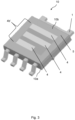
- FIG. 1d As shown in the various partial views of Figures 1a-1d , also combined with Figure 3 , an example of a semiconductor device according to the disclosure is presented.
- the final package is depicted in Figure 1d and 3 , and the semiconductor device is denoted with reference numeral 10. It comprises a lead frame 1 with a first lead frame surface 1a and a second lead frame surface 1b, opposite the first lead frame surface 1a, as well as a semiconductor die 3 comprising a first semiconductor die surface 3a and a second semiconductor die surface 3b, opposite the first semiconductor die surface 3a ( Figure 1b ).
- a clip 4 is implemented, which is composed of a flat part 4a and a corrugated part 4b.
- the corrugated part 4b comprises at least one peak 4b' and at least one valley 4b".
- the corrugated part 4b of the clip 4 comprises at least two peaks 4b', more in particular three peaks 4b'. However more than two peaks 4b' can be used, for example four peaks 4b'.
- the number of peaks 4b' contribute to an enlargement of the heat dissipating surface of the clip 4.
- the second lead frame surface 1b of the lead frame 1 is connected to the first semiconductor die surface 3a of the semiconductor die 3, and the second semiconductor die surface 3b of the semiconductor die 3 is connected to the corrugated part 4b of the clip 4, using a connection technique which will be outlined further in the detailed description.
- the complete assembly formed by the semiconductor die 3, the at least one valley 4b" of the corrugated part 4b of the clip 4, and the lead frame 1 are encapsulated by means of a mold compound 5.
- the encapsulated end product or package 10 is shown in Figure 1d , and shows that after encapsulation the mold compound 5 forms an outer surface of the semiconductor device 10 with at least one peak 4b' of the corrugated part 4b of the clip 4, at least part of the flat part 4a of the clip 4, and the first lead frame surface 1a of the lead frame 1 being exposed.
- the exposed elements of the package 10 effectively function as an enlarged heat dissipation surface, in particular at an upper or top face 10b of the semiconductor device 10.
- the exposed first lead frame surface 1a of the lead frame 1 forms the (first) lower surface 10a of the semiconductor device 10 and effectively functions as a drain terminal tab (also denoted with 1a).
- heat generated during operating the semiconductor device 10 is dissipated from an area with a high (hot) temperature towards an area with a lower (colder) temperature.
- the presence of additional heat sink functionality formed by the exposed corrugated part 4b' and flat part 4a of the clip 4 provides an additional heat dissipation at the upper surface 10b of the semiconductor device 10 aside from the commonly used heat sink formed by the drain terminal tab 1a. Accordingly, this configuration results in an improved electrical efficiency of the semiconductor device 10, e.g. formed as a MOSFET or transistor.
- the second lead frame surface 1b of the lead frame 1 is connected to the first semiconductor die surface 3a of the semiconductor die 3, and/or the second semiconductor die surface 3b of the semiconductor die 3 is connected to the corrugated part 4b of the clip 4 by means of soldering, sintering, or ultrasonic bonding.
- Soldering is the recommended process according to the example, as this allows for applying a required uniform solder volume, which prevents solder voids and/or insufficient soldering material.
- the connection between the lead frame 1 and the semiconductor die 3, and between the semiconductor die 3 and the clip 4 is schematically shown by means of reference numeral 2 (denoting for example solder paste) in Figure 1b and also in Figures 2b and 2d .
- the mold compound 5 and the at least one peak 4b' of the corrugated part 4b of the clip 4 form a single planar (upper) surface 10b of the semiconductor device 10, thus constituting an optimal heat sink surface with improved heat dissipation.
- the lead frame 1 and/or the clip 4 are made of a conductive metal sheet, for example copper or aluminum.
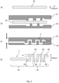
- the sheet has preferably a width of 200 ⁇ m, see Figure 4a .
- a width or thickness w of the corrugated part 4b is two times the width/thickness v of the metal sheet in between peaks 4b', see Figure 4d .
- Figures 2a-2g combined with Figures 1a-1d and Figures 4a-4d show the various steps of an example of a method of manufacturing a semiconductor device according to the disclosure.
- the method may comprise the steps of forming a clip 4 which comprises a flat part 4a and a corrugated part 4b, wherein the corrugated part comprises at least one peak 4b' and at least one valley 4b".
- the forming of such clip 4 is depicted in Figures 4a-4b and starts with a starting strip material 40 ( Figure 4a ) having a certain thickness D, which may be 200 ⁇ m.
- the starting strip material 40 is placed between two preform plates or press dies P1 and P2, which are provided with a preform shape, see Figure 4b .
- Both press dies P1 and P2 are moved towards each ( Figure 4c ) and form or punch the starting strip material 40 into the resulting clip 4 ( Figure 4d ) composed of a flat part 4a and a corrugated part 4b, wherein the corrugated part comprises at least one peak 4b' and at least one valley 4b".
- a width or thickness w of the corrugated part 4b is two times the width/thickness v of the metal sheet in between peaks 4b'.
- each corrugated clip 4 is accommodated in a so-called clip matrix 400, which contains a plurality of corrugated clips 4.
- the method of manufacturing the semiconductor device 10 continues with the step ii) of connecting a semiconductor die 3 to a lead frame 1.
- the lead frame 1 is shown in Figure 2a and in particular is depicted as a lead frame matrix (also denoted with reference numeral 1) suited for manufacturing a plurality of semiconductor devices in one sequence.
- the lead frame 1 is provided with several die attach paddles 1z which function as mounting surface of a semiconductor die 3.
- the lead frame 1 comprises a first lead frame surface 1a and a second lead frame surface 1b opposite the first lead frame surface 1a.
- the semiconductor die 3 comprises a first semiconductor die surface 3a and a second semiconductor die surface 3b opposite first semiconductor die surface 3a.
- the second lead frame surface 1b of the lead frame 1 is connected to the first semiconductor die surface 3a of the semiconductor die 3.
- Step iii) the clip 4 is connected to the semiconductor device 3 such that the second semiconductor die surface 3b of the semiconductor die 3 is connected to the corrugated part 4b of the clip 4.
- Step iii) can be facilitated by mounting the clip matrix 400 containing a plurality of corrugated clips 4 on to the lead frame matrix 1, such that the matrix of individual clips 4 exactly overlap with the plurality of semiconductor dies 3, each mounted to a die attach paddle 1z.
- the connecting steps ii) and iii) can be achieved by a multitude of connection techniques, such as soldering, sintering, or ultrasonic bonding between the second lead frame surface 1b of the lead frame 1 and the first semiconductor die surface 3a of the semiconductor die 3 and/or between the second semiconductor die surface 3b of the semiconductor die 3 and the corrugated part 4b of the clip 4.
- connection techniques such as soldering, sintering, or ultrasonic bonding between the second lead frame surface 1b of the lead frame 1 and the first semiconductor die surface 3a of the semiconductor die 3 and/or between the second semiconductor die surface 3b of the semiconductor die 3 and the corrugated part 4b of the clip 4.
- connection is schematically depicted by means of reference numeral 2, which might include a solder paste and solder material.
- reference numeral 2 might include a solder paste and solder material.
- soldering connection is performed, as soldering is the recommended process according to the example, as this allows for applying a required uniform solder volume, which prevents solder voids and/or insufficient soldering material.
- Figure 2f depicts the next method step iv) of encapsulating each assembly formed by the semiconductor die 3, the at least one valley 4b" of the corrugated part 4b of the clip 4, and the lead frame 1 with a mold compound 5.
- the resulting encapsulant packages are shown in Figure 2f wherein at least one peak 4b' of the corrugated part 4b of the clip 4, at least part of the flat part 4a of the clip 4, and the first lead frame surface 1a of the lead frame 1 are exposed. See also Figures 1d and 3 .
- the encapsulating step iv) results in the at least one peak 4b' of the corrugated part 4b of the clip 4 also being covered by the mold compound 5.
- This is depicted in Figure 1c and also in Figure 2f , wherein the corrugated parts 4b of each clip 4 are covered by mold compound 5, the covering being illustrated by depicting the peaks 4b' by means of dashed lines and with a shading which is slightly lighter than the shading of the mold compound 5.
- the encapsulating step iv) may be followed by a polishing step vi), see Figures 2g and 1d , such that the at least one peak 4b' of the corrugated part 4b of the clip 4 becomes exposed and the mold compound 5 and the at least one peak 4b' of the corrugated part 4b of the clip 4 forms a single plane surface.
- a polishing step vi see Figures 2g and 1d , such that the at least one peak 4b' of the corrugated part 4b of the clip 4 becomes exposed and the mold compound 5 and the at least one peak 4b' of the corrugated part 4b of the clip 4 forms a single plane surface.
- the semiconductor device is singulated from the lead frame matrix 1 and the clip matrix 400, through removal with known techniques of the excessive lead frame parts 1x and clip matrix parts 400x (see Figure 2g ).
Landscapes
- Lead Frames For Integrated Circuits (AREA)
Priority Applications (3)
| Application Number | Priority Date | Filing Date | Title |
|---|---|---|---|
| EP22203855.6A EP4362084A1 (de) | 2022-10-26 | 2022-10-26 | Halbleiterbauelement und verfahren zur herstellung solch eines halbleiterbauelements |
| CN202311380304.0A CN117936490A (zh) | 2022-10-26 | 2023-10-24 | 半导体器件和制造这种半导体器件的方法 |
| US18/494,946 US20240145354A1 (en) | 2022-10-26 | 2023-10-26 | Semiconductor device and a method for manufacturing such semiconductor device |
Applications Claiming Priority (1)
| Application Number | Priority Date | Filing Date | Title |
|---|---|---|---|
| EP22203855.6A EP4362084A1 (de) | 2022-10-26 | 2022-10-26 | Halbleiterbauelement und verfahren zur herstellung solch eines halbleiterbauelements |
Publications (1)
| Publication Number | Publication Date |
|---|---|
| EP4362084A1 true EP4362084A1 (de) | 2024-05-01 |
Family
ID=84044176
Family Applications (1)
| Application Number | Title | Priority Date | Filing Date |
|---|---|---|---|
| EP22203855.6A Pending EP4362084A1 (de) | 2022-10-26 | 2022-10-26 | Halbleiterbauelement und verfahren zur herstellung solch eines halbleiterbauelements |
Country Status (3)
| Country | Link |
|---|---|
| US (1) | US20240145354A1 (de) |
| EP (1) | EP4362084A1 (de) |
| CN (1) | CN117936490A (de) |
Citations (1)
| Publication number | Priority date | Publication date | Assignee | Title |
|---|---|---|---|---|
| US20170047274A1 (en) * | 2015-08-12 | 2017-02-16 | Texas Instruments Incorporated | Double Side Heat Dissipation for Silicon Chip Package |
-
2022
- 2022-10-26 EP EP22203855.6A patent/EP4362084A1/de active Pending
-
2023
- 2023-10-24 CN CN202311380304.0A patent/CN117936490A/zh active Pending
- 2023-10-26 US US18/494,946 patent/US20240145354A1/en active Pending
Patent Citations (1)
| Publication number | Priority date | Publication date | Assignee | Title |
|---|---|---|---|---|
| US20170047274A1 (en) * | 2015-08-12 | 2017-02-16 | Texas Instruments Incorporated | Double Side Heat Dissipation for Silicon Chip Package |
Also Published As
| Publication number | Publication date |
|---|---|
| CN117936490A (zh) | 2024-04-26 |
| US20240145354A1 (en) | 2024-05-02 |
Similar Documents
| Publication | Publication Date | Title |
|---|---|---|
| JP3467454B2 (ja) | 半導体装置の製造方法 | |
| TWI450373B (zh) | 雙側冷卻整合功率裝置封裝及模組,以及製造方法 | |
| US8546183B2 (en) | Method for fabricating heat dissipating semiconductor package | |
| US7410834B2 (en) | Method of manufacturing a semiconductor device | |
| EP1662565B1 (de) | Halbleiterpackung | |
| US20100133674A1 (en) | Compact Semiconductor Package with Integrated Bypass Capacitor and Method | |
| EP2058857A2 (de) | Integrierte Schaltungs-Chipverkapselung mit direkt angeschlossenen Leitungen | |
| US20050121756A1 (en) | Dual gauge leadframe | |
| US5299091A (en) | Packaged semiconductor device having heat dissipation/electrical connection bumps and method of manufacturing same | |
| CN113394119B (zh) | 半导体装置的制造方法以及半导体装置 | |
| JP3261965B2 (ja) | 半導体装置 | |
| EP3108503B1 (de) | Wandler mit teilweise verdünntem leiterrahmen mit gestapelten chips und zwischenstück | |
| TW200810069A (en) | Dual side cooling integrated power device package and module and methods of manufacture | |
| US20240178094A1 (en) | Semiconductor package | |
| JP2007184501A (ja) | 外部に露出する放熱体を上部に有する樹脂封止型半導体装置及びその製法 | |
| EP4362084A1 (de) | Halbleiterbauelement und verfahren zur herstellung solch eines halbleiterbauelements | |
| US8120169B2 (en) | Thermally enhanced molded leadless package | |
| CN118676081A (zh) | 一种高效散热的集成电路结构及其制备方法 | |
| EP4184566A1 (de) | Halbleiterbauelement und verfahren zur herstellung eines solchen halbleiterbauelements | |
| JPH10256455A (ja) | ダイ・パッドをオフセットさせた半導体パッケージ及びその製造方法 | |
| US20250357282A1 (en) | Device package having a cavity with sloped sidewalls | |
| EP4345891A2 (de) | Leistungsrahmengehäuse mit reduzierten löthohlräumen | |
| US20240222234A1 (en) | Package with low-warpage carrier | |
| CN101421840A (zh) | 具有双暴露表面的封装式半导体装置及其制造方法 | |
| CN120164867A (zh) | 半导体器件及其制造方法 |
Legal Events
| Date | Code | Title | Description |
|---|---|---|---|
| PUAI | Public reference made under article 153(3) epc to a published international application that has entered the european phase |
Free format text: ORIGINAL CODE: 0009012 |
|
| STAA | Information on the status of an ep patent application or granted ep patent |
Free format text: STATUS: THE APPLICATION HAS BEEN PUBLISHED |
|
| AK | Designated contracting states |
Kind code of ref document: A1 Designated state(s): AL AT BE BG CH CY CZ DE DK EE ES FI FR GB GR HR HU IE IS IT LI LT LU LV MC ME MK MT NL NO PL PT RO RS SE SI SK SM TR |
|
| STAA | Information on the status of an ep patent application or granted ep patent |
Free format text: STATUS: REQUEST FOR EXAMINATION WAS MADE |
|
| 17P | Request for examination filed |
Effective date: 20241101 |
|
| RBV | Designated contracting states (corrected) |
Designated state(s): AL AT BE BG CH CY CZ DE DK EE ES FI FR GB GR HR HU IE IS IT LI LT LU LV MC ME MK MT NL NO PL PT RO RS SE SI SK SM TR |