EP4361827A2 - Planung von speicheranfragen für eine gekoppelte speichervorrichtung - Google Patents
Planung von speicheranfragen für eine gekoppelte speichervorrichtung Download PDFInfo
- Publication number
- EP4361827A2 EP4361827A2 EP24158174.3A EP24158174A EP4361827A2 EP 4361827 A2 EP4361827 A2 EP 4361827A2 EP 24158174 A EP24158174 A EP 24158174A EP 4361827 A2 EP4361827 A2 EP 4361827A2
- Authority
- EP
- European Patent Office
- Prior art keywords
- memory
- data
- address
- request
- memory request
- Prior art date
- Legal status (The legal status is an assumption and is not a legal conclusion. Google has not performed a legal analysis and makes no representation as to the accuracy of the status listed.)
- Pending
Links
Images



Classifications
-
- G—PHYSICS
- G06—COMPUTING OR CALCULATING; COUNTING
- G06F—ELECTRIC DIGITAL DATA PROCESSING
- G06F3/00—Input arrangements for transferring data to be processed into a form capable of being handled by the computer; Output arrangements for transferring data from processing unit to output unit, e.g. interface arrangements
- G06F3/06—Digital input from, or digital output to, record carriers, e.g. RAID, emulated record carriers or networked record carriers
- G06F3/0601—Interfaces specially adapted for storage systems
- G06F3/0602—Interfaces specially adapted for storage systems specifically adapted to achieve a particular effect
- G06F3/061—Improving I/O performance
- G06F3/0611—Improving I/O performance in relation to response time
-
- G—PHYSICS
- G06—COMPUTING OR CALCULATING; COUNTING
- G06F—ELECTRIC DIGITAL DATA PROCESSING
- G06F3/00—Input arrangements for transferring data to be processed into a form capable of being handled by the computer; Output arrangements for transferring data from processing unit to output unit, e.g. interface arrangements
- G06F3/06—Digital input from, or digital output to, record carriers, e.g. RAID, emulated record carriers or networked record carriers
- G06F3/0601—Interfaces specially adapted for storage systems
- G06F3/0628—Interfaces specially adapted for storage systems making use of a particular technique
- G06F3/0655—Vertical data movement, i.e. input-output transfer; data movement between one or more hosts and one or more storage devices
- G06F3/0659—Command handling arrangements, e.g. command buffers, queues, command scheduling
-
- G—PHYSICS
- G06—COMPUTING OR CALCULATING; COUNTING
- G06F—ELECTRIC DIGITAL DATA PROCESSING
- G06F9/00—Arrangements for program control, e.g. control units
- G06F9/06—Arrangements for program control, e.g. control units using stored programs, i.e. using an internal store of processing equipment to receive or retain programs
- G06F9/46—Multiprogramming arrangements
- G06F9/50—Allocation of resources, e.g. of the central processing unit [CPU]
- G06F9/5005—Allocation of resources, e.g. of the central processing unit [CPU] to service a request
- G06F9/5011—Allocation of resources, e.g. of the central processing unit [CPU] to service a request the resources being hardware resources other than CPUs, Servers and Terminals
-
- G—PHYSICS
- G06—COMPUTING OR CALCULATING; COUNTING
- G06F—ELECTRIC DIGITAL DATA PROCESSING
- G06F12/00—Accessing, addressing or allocating within memory systems or architectures
- G06F12/02—Addressing or allocation; Relocation
- G06F12/08—Addressing or allocation; Relocation in hierarchically structured memory systems, e.g. virtual memory systems
- G06F12/10—Address translation
-
- G—PHYSICS
- G06—COMPUTING OR CALCULATING; COUNTING
- G06F—ELECTRIC DIGITAL DATA PROCESSING
- G06F13/00—Interconnection of, or transfer of information or other signals between, memories, input/output devices or central processing units
- G06F13/14—Handling requests for interconnection or transfer
- G06F13/16—Handling requests for interconnection or transfer for access to memory bus
- G06F13/1605—Handling requests for interconnection or transfer for access to memory bus based on arbitration
- G06F13/161—Handling requests for interconnection or transfer for access to memory bus based on arbitration with latency improvement
- G06F13/1626—Handling requests for interconnection or transfer for access to memory bus based on arbitration with latency improvement by reordering requests
- G06F13/1631—Handling requests for interconnection or transfer for access to memory bus based on arbitration with latency improvement by reordering requests through address comparison
-
- G—PHYSICS
- G06—COMPUTING OR CALCULATING; COUNTING
- G06F—ELECTRIC DIGITAL DATA PROCESSING
- G06F13/00—Interconnection of, or transfer of information or other signals between, memories, input/output devices or central processing units
- G06F13/14—Handling requests for interconnection or transfer
- G06F13/16—Handling requests for interconnection or transfer for access to memory bus
- G06F13/1668—Details of memory controller
- G06F13/1684—Details of memory controller using multiple buses
-
- G—PHYSICS
- G06—COMPUTING OR CALCULATING; COUNTING
- G06F—ELECTRIC DIGITAL DATA PROCESSING
- G06F3/00—Input arrangements for transferring data to be processed into a form capable of being handled by the computer; Output arrangements for transferring data from processing unit to output unit, e.g. interface arrangements
- G06F3/06—Digital input from, or digital output to, record carriers, e.g. RAID, emulated record carriers or networked record carriers
- G06F3/0601—Interfaces specially adapted for storage systems
- G06F3/0628—Interfaces specially adapted for storage systems making use of a particular technique
- G06F3/0655—Vertical data movement, i.e. input-output transfer; data movement between one or more hosts and one or more storage devices
- G06F3/0658—Controller construction arrangements
-
- G—PHYSICS
- G06—COMPUTING OR CALCULATING; COUNTING
- G06F—ELECTRIC DIGITAL DATA PROCESSING
- G06F3/00—Input arrangements for transferring data to be processed into a form capable of being handled by the computer; Output arrangements for transferring data from processing unit to output unit, e.g. interface arrangements
- G06F3/06—Digital input from, or digital output to, record carriers, e.g. RAID, emulated record carriers or networked record carriers
- G06F3/0601—Interfaces specially adapted for storage systems
- G06F3/0668—Interfaces specially adapted for storage systems adopting a particular infrastructure
- G06F3/0671—In-line storage system
- G06F3/0673—Single storage device
-
- G—PHYSICS
- G06—COMPUTING OR CALCULATING; COUNTING
- G06F—ELECTRIC DIGITAL DATA PROCESSING
- G06F13/00—Interconnection of, or transfer of information or other signals between, memories, input/output devices or central processing units
- G06F13/14—Handling requests for interconnection or transfer
- G06F13/16—Handling requests for interconnection or transfer for access to memory bus
- G06F13/1605—Handling requests for interconnection or transfer for access to memory bus based on arbitration
- G06F13/161—Handling requests for interconnection or transfer for access to memory bus based on arbitration with latency improvement
- G06F13/1626—Handling requests for interconnection or transfer for access to memory bus based on arbitration with latency improvement by reordering requests
-
- G—PHYSICS
- G06—COMPUTING OR CALCULATING; COUNTING
- G06F—ELECTRIC DIGITAL DATA PROCESSING
- G06F2212/00—Indexing scheme relating to accessing, addressing or allocation within memory systems or architectures
- G06F2212/10—Providing a specific technical effect
- G06F2212/1016—Performance improvement
- G06F2212/1024—Latency reduction
Definitions
- a variety of computing devices utilize heterogeneous integration, which integrates multiple types of ICs for providing system functionality.
- the multiple functions include audio/video (A/V) data processing, other high data parallel applications for the medicine and business fields, processing instructions of a general-purpose instruction set architecture (ISA), digital, analog, mixed-signal and radio-frequency (RF) functions, and so forth.
- the performance of one or more computing systems can depend on the processing node.
- the processing node is used within a mobile computing device running several different types of applications and possibly relaying information to multiple users (both local and remote) at one time.
- the processing node is used within a desktop.
- the processing node is one of multiple processing nodes in a socket of a multi-socket server. The server is used to provide services to other computer programs in remote computing devices as well as computer programs within the server.
- the memory hierarchy in each of the above variety of computing systems transitions from relatively fast, volatile memory, such as registers on a processor die and caches either located on the processor die or connected to the processor die, to non-volatile and relatively slow memory such as magnetic hard disks.
- the memory hierarchy provides challenges to maintain high performance for quick access demands by the running computer programs.
- One challenge is reducing the amount of time in system memory, which is the random access memory (RAM) located beyond the cache subsystems, but does not include the non-volatile disk memory.
- RAM random access memory
- SDRAM Synchronous dynamic RAM
- other conventional memory technologies reduce the stall time of system memory due to limited bandwidth, but the access latency does not improve with these techniques.
- an appreciable amount of on-die area and power consumption are used to support interfaces and protocols to access the data stored in system memory.
- a computing system includes one or more clients for processing applications.
- clients are a general-purpose central processing unit (CPU), a graphics processing unit (GPU), an accelerated processing unit (APU), an input/output (I/O) device and so forth.
- a memory controller is configured to transfer traffic between the memory controller and two channels, each connected to a memory device.
- one or more of the two memory devices is one of a variety of random access memories (RAMs) on a dual in-line memory module (DIMM).
- RAMs random access memories
- DIMM dual in-line memory module
- one or more of the two memory devices is a planar mounted RAM device, which is a RAM device that is either socketed or soldered onto a motherboard.
- one or more of the two memory devices is a three-dimensional integrated circuit (3D IC).
- a command processor in the memory controller translates memory requests received from clients to commands to be processed by the selected type(s) of memory devices.
- a client sends a 64-byte memory request with an indication specifying that there are two 32-byte requests targeting non-contiguous data within a same page.
- the memory controller generates two addresses.
- the memory controller sends a single command and the two addresses to two channels to access data in a same page.
- the memory controller sends the separate, generated two addresses, or a portion thereof, to the two channels.
- one address is an offset relative to the other address of the two generated addresses.
- the single command with the two addresses accesses non-contiguous data in the same page. In other embodiments, the single command with the two addresses accesses contiguous data in the same page.
- the memory controller does not transfer 64 bytes for a single 32-byte memory request and discards 32 bytes of the 64 bytes, which is inefficient. Rather, the memory controller transfers 64 bytes for two 32-byte memory requests accessing data within a range of memory addresses such as within a page of memory.
- FIG. 1 a generalized block diagram of one embodiment of a computing system 100 is shown.
- clients 110 and 112 send memory requests to memory controllers 130A and 130B via data fabric 120.
- each memory controller has a single memory channel capable of sending two addresses.
- memory controller 130A includes memory channel 140A with address generator 142A and address generator 144A.
- memory controller 130B includes memory channel 140B with address generator 142B and address generator 144B.
- Memory controller 130A transfers commands, addresses and data on channels 152A and 154A to memory devices 160A and 162A.
- Memory controller 130B transfers commands, addresses and data on channels 152B and 154B to memory devices 160B and 162B.
- I/O input/output
- the components of computing system 100 are individual dies on an integrated circuit (IC), such as a system-on-a-chip (SOC).
- IC integrated circuit
- the components are individual dies in a system-in-package (SiP) or a multi-chip module (MCM).
- clients 110 and 112 include one or more of a central processing unit (CPU), a graphics processing unit (GPU), a hub for a multimedia engine, and so forth.
- CPU central processing unit
- GPU graphics processing unit
- hub for a multimedia engine
- each of the one or more processor cores in the CPU includes circuitry for executing instructions according to a given selected instruction set architecture (ISA).
- ISA selected instruction set architecture
- each of the processor cores in the CPU includes a superscalar, multi-threaded microarchitecture used for processing instructions of the given ISA.
- graphics processing unit GPU
- it includes a high parallel data microarchitecture with a significant number of parallel execution lanes.
- the microarchitecture uses single-instruction-multiple-data (SIMD) pipeline for the parallel execution lanes.
- SIMD single-instruction-multiple-data
- communication fabric 120 transfers traffic back and forth between clients 110 and 112 and memory controllers 130A and 130B.
- Data fabric 120 includes interfaces for supporting respective communication protocols.
- communication fabric 120 includes queues for storing requests and responses, selection logic for arbitrating between received requests before sending requests across an internal network, logic for building and decoding packets, and logic for selecting routes for the packets.
- memory controllers 130A-130B receive memory requests from clients 110-112 via communication fabric 120, translate the memory requests to commands, and send the commands to one or more of off-chip disk memory (not shown) and system memory, which is implemented as one of a variety of random access memories (RAMs) in memory devices 160A, 162A, 160B and 162B.
- Memory controller 130 also receives responses from memory devices 160A, 162A, 160B and 162B and disk memory and sends the responses to a corresponding source of clients 110-112.
- the address space of the computing system 100 is divided among at least clients 110-112 and one or more other components such as input/output peripheral devices (not shown) and other types of computing resources.
- Memory maps are maintained for determining which addresses are mapped to which component, and hence to which one of clients 110-112 a memory request for a particular address should be routed.
- clients 110-112 include cache memory subsystems to reduce memory latencies for a respective processor core.
- a shared cache memory subsystem is used by processor cores as a last-level cache (LLC) before accessing memory devices 160A, 162A, 160B and 162B.
- memory access refers to performing a memory read request or a memory write request operation that results in a cache hit if the requested data of a corresponding request address resides in the cache.
- the memory access request results in a cache miss if the requested data does not reside in the cache.
- system memory includes a multi-channel memory architecture.
- This type of architecture increases the transfer speed of data to memory controllers 130A and 130B by adding more channels of communication between them such as channels 152A, 154A, 152B and 154B.
- the multi-channel architecture utilizes multiple memory modules and a motherboard and/or a card capable of supporting multiple channels.
- computing system 100 utilizes one of a variety of dynamic RAM (DRAM) to provide system memory.
- computing system 100 utilizes three-dimensional integrated circuits (3D ICs) to provide system memory.
- 3D integrated DRAM provides both low-latency interconnects and additional on-chip memory storage to reduce off-chip memory accesses.
- Other memory technologies for system memory that use a row-based access scheme including one or more row buffers or other equivalent structures are possible and contemplated. Examples of other memory technologies include phase-change memories, spin-torque-transfer resistive memories, memristors, and so forth.
- each one of channels 152A, 154A, 152B and 154B is a link, which includes a command bus, an address bus and a data bus for multiple banks within a respective one of memory devices 160A, 162A, 160B and 162B.
- memory devices 160A, 162A, 160B and 162B include multiple ranks, each with multiple memory array banks.
- Each of the banks includes multiple rows and a row buffer.
- Each row buffer stores data corresponding to an accessed row of the multiple rows within the memory array banks.
- the accessed row is identified by a DRAM address in the received memory request.
- each row stores a page of data.
- the size of the page is chosen based on design considerations. Such a page size can be one kilobyte (1 KB), four kilobytes (4 KB), or any other size.
- Memory channels 140A and 140B interface with PHY 150A and 150B.
- each of the physical interfaces PHY 150A and 150B convey a stream of commands from memory controllers 130A and 130B to memory devices 160A, 162A, 160B and 162B with a given timing.
- a protocol determines values used for information transfer, such as a number of data transfers per clock cycle, signal voltage levels, signal timings, signal and clock phases and clock frequencies.
- each of PHY 150A and 150B include a state machine for initialization and calibration sequences specified in the protocol.
- each of PHY 150A and 150B include self-test, diagnostic, and error-detection and correction hardware.
- Protocol examples for a respective interface between PHY 150A and 150B and memory devices 160A, 162A, 160B and 162B include DDR2 SDRAM, DDR3 SDRAM, GDDR4 (Graphics Double Data Rate, version 4) SDRAM, GDDR5 SDRAM, and GDDR6 SDRAM.
- memory channel 140A includes address generators 142A and 144A
- memory channel 140B includes address generators 142B and 144B.
- address generators 142A and 144A translate a memory request address received by memory controller 130A to values identifying a given rank, a given bank and a given row in one of the memory devices 160A and 162A. Although two address generators are shown, in other embodiments, another number of address generators are included in memory controller 130A.
- address generator 144A generates a second address as an offset relative to a first address generated by address generator 142A. In one embodiment, address generator 144A uses the same identifiers in the second address as does the first address generated by address generator 142A for identifying a given rank and a given bank and a given row within one of the memory devices 160A and 162A. In addition, in an embodiment, the first address identifies a starting byte of requested first data in the identified row and the second address identifies a starting byte of requested second data that does not overlap the first data. In an embodiment, the second data is contiguous with the first data in the identified row. In other embodiments, the second data is not contiguous with the first data in the identified row. Therefore, the single memory controller 130A transfers data and commands to the two channels 152A and 154A while also supporting simultaneous access to data in a same row for two different requests.
- control unit 132A stores an indication that a given memory access command services each of a first memory request and a second memory request different from the first memory request when control unit 132A determines each of the first memory request and the second memory request targets data within a given range of memory addresses.
- the given range of memory addresses is a range for a page of memory in one of memory devices 160A and 162A.
- control unit 130A marks each of the first memory request and the second memory request as complete responsive to determining the given memory access command has completed.
- memory controller 200 includes an interface 210 to computing resources via a communication fabric, queues 220 for storing received memory access requests and received responses, control unit 250 and an interface 280 to memory devices via at least a physical interface and at least two channels.
- interfaces 210 and 280 supports respective communication protocols.
- queues 220 includes a read queue 232 for storing received read requests and a separate write queue 234 for storing received write requests. In other embodiments, queues 220 includes a unified queue for storing both memory read requests and memory write requests. In one embodiment, queues 220 includes queue 236 for storing scheduled memory access requests selected from read queue 232, write queue 234 or a unified queue if one is used. Queue 236 is also referred to as pending queue 236. In some embodiments, control registers 270 store an indication of a current mode. For example, the off-chip memory data bus and memory device support either a read mode or a write mode at a given time. Therefore, traffic is routed in a given single direction during the current mode and changes direction when the current mode ends.
- read scheduler 252 includes arbitration logic for selecting read requests from the read queue 232 out-of-order.
- Read scheduler 252 schedules the out-of-order issue of the stored requests within the read queue 232 to the memory device based on a quality-of-service (QoS) or other priority information, age, a process or thread identifier (ID), and a relationship with other stored requests such as targeting a same memory channel, targeting a same rank, targeting a same bank and/or targeting a same page.
- QoS quality-of-service
- ID process or thread identifier
- Write scheduler 254 includes similar selection logic for the write queue 234.
- response scheduler 256 includes similar logic for issuing, based on priorities, responses out-of-order to the computing resources, which were received from the memory device.
- command processor 272 translates received memory requests to one or more transactions (or commands) such as read/write transactions and activation and precharge transactions.
- the commands are stored in queues 232-236. In other embodiments, a separate set of queues are used.
- control unit 250 includes address generators 260 and 262.
- address generators 260 and 262 translate a memory request address received by memory controller 130A to values identifying a given rank, a given bank and a given row in one of the memory devices connected to memory controller 200. Although two address generators are shown, in other embodiments, another number of address generators are included in control unit 250.
- address generator 262 generates a second address as an offset relative to a first address generated by address generator 260. In one embodiment, address generator 262 uses the same identifiers in the second address as does the first address for identifying a given rank and a given bank and a given row within one of the memory devices. In addition, in an embodiment, the first address identifies a starting byte of requested data in the identified row and the second address identifies a starting byte of requested data that does not overlap the first data and it is not contiguous with the first data in the identified row. Therefore, the single memory controller 200 transfers data and commands to at least two channels while also supporting simultaneous access to non-contiguous data.
- control unit 250 stores an indication that a given memory access command stored in queues 220 services each of a first memory request and a second memory request different from the first memory request stored in queues 220 when control unit 250 determines each of the first memory request and the second memory request targets data within a given range of memory addresses.
- the given range of memory addresses is an address range for a page of memory in one of the memory devices.
- control unit 250 marks each of the first memory request and the second memory request as complete responsive to determining the given memory access command has completed.
- control registers 270 store an indication of a current mode. For example, the memory data bus and memory device support either a read mode or a write mode at a given time. Therefore, traffic is routed in a given single direction during the current mode and changes direction when the current mode is changed after a data bus turnaround latency.
- control registers 270 store a threshold number of read requests (read burst length) to send during the read mode.
- control registers 270 store weights for criteria used by selection algorithms in read scheduler 252 and write scheduler 254 for selecting requests stored in queues 232-236 to issue.
- each of the at least two channels connected to memory controller 200 via a physical interface receives a same command accessing data in a same page within a selected memory device.
- each channel has its own address.
- a first channel receives a first address from address generator 260 and a second channel different from the first channel receives a second address from address generator 262.
- the addresses generated by address generators 260 and 262 are column addresses for DRAM.
- memory controller 200 simultaneously accesses non-contiguous data.
- memory controller 200 supports the GDDR6 DRAM protocol.
- interface 280 supports read and write transactions per channel (of the two channels) with a width of 16 bits (2 bytes) and the burst length is 16.
- the two ganged 16-bit wide channels provide the equivalent of a 32-bit (4 byte) wide channel. For 64-byte requests, the 32-bit (4 byte) wide equivalent channel provided by the two channels and the burst length of 16 transfers 64 bytes for servicing a 64-byte memory request.
- the two channels are ganged and memory controller 200 manages both 16-bit wide interfaces.
- control unit 250 manages the 64-byte interface as two independent 32-byte interfaces for 32-byte requests.
- control unit 250 sends commands to simultaneously open the same page across both 16-bit channels. For example, control unit 250 issues an activate command to each of the two channels at the same time, and issues a memory access command to each of the two channels at the same time, but control unit 250 sends two different addresses via address generators 260 and 262 to simultaneously and independently access the opened page. Neighboring data (within the same page), which is also non-contiguous data, are accessed simultaneously. Therefore, memory controller 200 does not transfer 64 bytes for a single 32-byte memory request and discards 32 bytes of the 64 bytes, which is inefficient. Rather, memory controller 200 transfers 64 bytes for two 32-byte memory requests accessing non-contiguous data within a range of memory addresses such as within a page of memory.
- control unit 250 determines when two 32-byte memory requests access non-contiguous data within a same page in one of the memory devices.
- a client such as a GPU, determines when two 32-byte memory requests access a same page in one of the memory devices. The client sends a 64-byte memory request with an indication specifying that there are two 32-byte requests targeting non-contiguous data within a same page.
- control unit 250 issues a 64-byte command, the address from address generator 262 is ignored.
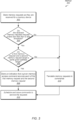
- FIG. 3 one embodiment of a method 300 for performing efficient memory accesses for a computing system is shown.
- the steps in this embodiment are shown in sequential order.
- one or more of the elements described are performed concurrently, in a different order than shown, or are omitted entirely.
- Other additional elements are also performed as desired. Any of the various systems or apparatuses described herein are configured to implement method 300.
- One or more clients execute computer programs, or software applications.
- the client determines a given memory access request misses within a cache memory subsystem and sends the memory access request to system memory via a memory controller.
- the memory requests are stored as they are received (block 302). If the received memory requests do not request data with a data size less than a size threshold ("no" branch of the conditional block 304), then memory requests are translated to commands (block 310).
- memory requests request data with sizes of 64 bytes and 32 bytes.
- the size threshold is set at 64 bytes. Therefore, a memory request requesting data with a data size of 64 bytes does not request data with a data size less than the size threshold.
- a memory request such as a memory read request
- a memory read request is converted into one or more commands based on the memory being accessed.
- control logic within DRAM performs complex transactions such as activation (opening) transactions and precharge of data and control lines within DRAM once to access an identified row and once to put back the modified contents stored in the row buffer to the identified row during a close transaction.
- activation opening
- precharge precharge of data and control lines within DRAM once to access an identified row and once to put back the modified contents stored in the row buffer to the identified row during a close transaction.
- Each of the different DRAM transactions such as activation/open, column access, read access, write access, and precharge/close, has a different respective latency.
- the memory access commands are scheduled for issue to service the memory requests (block 312).
- the memory access commands are marked for out-of-order issue based at least upon priorities and targets of the corresponding memory requests.
- the memory requests are scheduled prior to translation to commands. Therefore, the memory controller supports out-of-order issue for the memory requests.
- method 300 moves to block 310 where memory requests are translated to commands.
- the received memory requests have a data size less than a size of the memory data bus ("yes" branch of the conditional block 304), and a first memory request and a second memory request target a same given address range ("yes" branch of the conditional block 306), then an indication that a given memory access command services each of the first memory request and the second memory request is stored (block 308). Afterward, method 300 moves to block 310 where memory requests are translated to commands.
- FIG. 4 one embodiment of a method 400 for performing efficient memory accesses for a computing system is shown.
- An indication is detected that a given memory access command services each of a first memory request and a second memory request (block 402).
- the given memory access command is sent to a memory device (block 404).
- scheduling logic in a memory controller selects the given memory access command for issue to the memory device based on priority levels, age, and so forth.
- the memory controller sends to the memory device a first address pointing to a first location in the memory device storing first data (block 406).
- the memory controller sends to the memory device a second address pointing to a second location in the memory device storing second data that is non-contiguous with the first data (block 408).
- Each of the first memory request and the second memory request are marked as complete responsive to determining the given memory access command has completed (block 410).
- program instructions of a software application are used to implement the methods and/or mechanisms previously described.
- the program instructions describe the behavior of hardware in a high-level programming language, such as C.
- a hardware design language HDL
- the program instructions are stored on a non-transitory computer readable storage medium. Numerous types of storage media are available.
- the storage medium is accessible by a computing system during use to provide the program instructions and accompanying data to the computing system for program execution.
- the computing system includes at least one or more memories and one or more processors configured to execute program instructions.
- a memory controller comprising a first interface for receiving memory requests; a second interface comprising: a command bus for sending memory access commands corresponding to the memory requests to a memory device; a first address bus for sending addresses to the memory device; and a second address bus for sending addresses to the memory device; control logic, wherein in response to determining a given memory access command is scheduled to be issued at a given point in time, the control logic is configured to:
- control logic is further configured to store an indication that the given memory access command services each of the first memory request and the second memory request, in response to determining each of the first memory request and the second memory request targets data within a given range of memory addresses.
- Clause 3 The memory controller as recited in clause 2, wherein the given range of memory addresses is a range for a page of memory.
- Clause 4 The memory controller as recited in clause 1, wherein a first memory request includes an address pointing to the first location and a second memory request includes an address pointing to the second location.
- Clause 7 The memory controller as recited in clause 1, wherein the second interface further comprises a data bus for transferring data between the memory controller and the memory device, and wherein each of the first data and the second data has a size less than a size threshold.
- Clause 8 The memory controller as recited in clause 7, wherein the first data and the second data are transferred simultaneously on the data bus.
- control logic is further configured to mark each of a first memory request and a second memory request different from the first memory request as complete responsive to determining the given memory access command has completed.
- Clause 10 There is provided a method, comprising: receiving, by a first interface, memory requests; sending, by a command bus in a second interface, memory access commands corresponding to the memory requests to a memory device; sending, by a first address bus in the second interface, addresses to the memory device; sending, by a second address bus in the second interface, addresses to the memory device; in response to determining a given memory access command is scheduled to be issued at a given point in time: sending at the given point in time the given memory access command to the memory device; sending at the given point in time a first address on the first address bus, wherein the first address points to a first location in the memory device storing first data; and sending at the given point in time a second address on the second address bus, wherein the second address points to a second location in the memory device storing second data that is non-contiguous with the first data.
- Clause 11 The method as recited in clause 10, further comprising storing an indication that the given memory access command services each of a first memory request and a second memory request, in response to determining each of the first memory request and the second memory request targets data within a given range of memory addresses.
- Clause 12 The method as recited in clause 10, wherein a first memory request includes an address pointing to the first location and a second memory request includes an address pointing to the second location.
- Clause 14 The method as recited in clause 10, wherein the given memory access command accesses each of the first data and the second data.
- Clause 15 The method as recited in clause 10, wherein the second interface further comprises a data bus for transferring data between the memory controller and the memory device, and wherein each of the first data and the second data has a size less than a size threshold.
- Clause 16 The method as recited in clause 10, further comprising marking each of a first memory request and a second memory request different from the first memory request as complete responsive to determining the given memory access command has completed.
- a computing system comprising: a processor configured to generate memory access requests for data stored in a memory device; and a memory controller coupled to the memory device; wherein in response to determining a given memory access command is scheduled to be issued at a given point in time, the memory controller is configured to: send at the given point in time the given memory access command to the memory device; send at the given point in time a first address on the first address bus, wherein the first address points to a first location in the memory device storing first data; and send at the given point in time a second address on the second address bus, wherein the second address points to a second location in the memory device storing second data that is non-contiguous with the first data.
- Clause 18 The computing system as recited in clause 17, wherein the memory controller is further configured to store an indication that the given memory access command services each of a first memory request and a second memory request, in response to determining each of the first memory request and the second memory request targets data within a given range of memory addresses.
- Clause 19 The computing system as recited in clause 17, wherein the second address is an offset relative to the first address.
- Clause 20 The computing system as recited in clause 17, wherein the memory controller is further configured to mark each of a first memory request and a second memory request different from the first memory request as complete responsive to determining the given memory access command has completed.
Landscapes
- Engineering & Computer Science (AREA)
- Theoretical Computer Science (AREA)
- Physics & Mathematics (AREA)
- General Engineering & Computer Science (AREA)
- General Physics & Mathematics (AREA)
- Human Computer Interaction (AREA)
- Software Systems (AREA)
- Memory System Of A Hierarchy Structure (AREA)
- Memory System (AREA)
- Dram (AREA)
Applications Claiming Priority (3)
| Application Number | Priority Date | Filing Date | Title |
|---|---|---|---|
| US15/851,479 US11422707B2 (en) | 2017-12-21 | 2017-12-21 | Scheduling memory requests for a ganged memory device |
| PCT/US2018/051791 WO2019125563A1 (en) | 2017-12-21 | 2018-09-19 | Scheduling memory requests for a ganged memory device |
| EP18789522.2A EP3729267A1 (de) | 2017-12-21 | 2018-09-19 | Planung von speicheranfragen für eine ganged-memory-vorrichtung |
Related Parent Applications (1)
| Application Number | Title | Priority Date | Filing Date |
|---|---|---|---|
| EP18789522.2A Division EP3729267A1 (de) | 2017-12-21 | 2018-09-19 | Planung von speicheranfragen für eine ganged-memory-vorrichtung |
Publications (2)
| Publication Number | Publication Date |
|---|---|
| EP4361827A2 true EP4361827A2 (de) | 2024-05-01 |
| EP4361827A3 EP4361827A3 (de) | 2024-07-17 |
Family
ID=63915096
Family Applications (2)
| Application Number | Title | Priority Date | Filing Date |
|---|---|---|---|
| EP18789522.2A Ceased EP3729267A1 (de) | 2017-12-21 | 2018-09-19 | Planung von speicheranfragen für eine ganged-memory-vorrichtung |
| EP24158174.3A Pending EP4361827A3 (de) | 2017-12-21 | 2018-09-19 | Planung von speicheranfragen für eine gekoppelte speichervorrichtung |
Family Applications Before (1)
| Application Number | Title | Priority Date | Filing Date |
|---|---|---|---|
| EP18789522.2A Ceased EP3729267A1 (de) | 2017-12-21 | 2018-09-19 | Planung von speicheranfragen für eine ganged-memory-vorrichtung |
Country Status (6)
| Country | Link |
|---|---|
| US (1) | US11422707B2 (de) |
| EP (2) | EP3729267A1 (de) |
| JP (1) | JP7384806B2 (de) |
| KR (1) | KR102789083B1 (de) |
| CN (1) | CN111656322B (de) |
| WO (1) | WO2019125563A1 (de) |
Families Citing this family (9)
| Publication number | Priority date | Publication date | Assignee | Title |
|---|---|---|---|---|
| US11054998B1 (en) | 2019-12-12 | 2021-07-06 | Facebook, Inc. | High bandwidth memory system with distributed request broadcasting masters |
| KR102804852B1 (ko) * | 2019-12-23 | 2025-05-09 | 주식회사 엘엑스세미콘 | 메모리 컨트롤러, 및 이의 동작 방법 |
| US20210200694A1 (en) * | 2019-12-27 | 2021-07-01 | Advanced Micro Devices, Inc. | Staging buffer arbitration |
| WO2022035075A1 (ko) | 2020-08-10 | 2022-02-17 | 주식회사 큐티스의 생명연구센터 | 마이크로니들 패치를 포함하는 최소 침습적 피부 상태 진단 키트 |
| US11494316B2 (en) * | 2020-08-24 | 2022-11-08 | Advanced Micro Devices, Inc. | Memory controller with a plurality of command sub-queues and corresponding arbiters |
| US11775197B2 (en) * | 2021-03-25 | 2023-10-03 | Kyocera Document Solutions Inc. | Single command for reading then clearing dynamic random access memory |
| US20220374237A1 (en) * | 2021-05-21 | 2022-11-24 | Telefonaktiebolaget Lm Ericsson (Publ) | Apparatus and method for identifying and prioritizing certain instructions in a microprocessor instruction pipeline |
| CN115391105B (zh) * | 2022-08-31 | 2025-07-18 | 杭州宏杉科技股份有限公司 | 一种应用于存储设备的存储控制方法和装置 |
| TWI854298B (zh) * | 2022-09-13 | 2024-09-01 | 創鑫智慧股份有限公司 | 記憶體查找裝置及方法 |
Family Cites Families (30)
| Publication number | Priority date | Publication date | Assignee | Title |
|---|---|---|---|---|
| JP2932855B2 (ja) * | 1992-09-08 | 1999-08-09 | 日本電気株式会社 | 多重入出力メモリ |
| US5446855A (en) * | 1994-02-07 | 1995-08-29 | Buslogic, Inc. | System and method for disk array data transfer |
| JP2000099397A (ja) * | 1998-09-18 | 2000-04-07 | Hitachi Ltd | データ処理装置 |
| US6526484B1 (en) | 1998-11-16 | 2003-02-25 | Infineon Technologies Ag | Methods and apparatus for reordering of the memory requests to achieve higher average utilization of the command and data bus |
| US6195727B1 (en) * | 1999-03-31 | 2001-02-27 | International Business Machines Corporation | Coalescing raid commands accessing contiguous data in write-through mode |
| US6457078B1 (en) | 1999-06-17 | 2002-09-24 | Advanced Micro Devices, Inc. | Multi-purpose bi-directional control bus for carrying tokens between initiator devices and target devices |
| US6912173B2 (en) * | 2001-06-29 | 2005-06-28 | Broadcom Corporation | Method and system for fast memory access |
| US6944731B2 (en) * | 2001-12-19 | 2005-09-13 | Agere Systems Inc. | Dynamic random access memory system with bank conflict avoidance feature |
| US6839797B2 (en) * | 2001-12-21 | 2005-01-04 | Agere Systems, Inc. | Multi-bank scheduling to improve performance on tree accesses in a DRAM based random access memory subsystem |
| US7130933B2 (en) * | 2002-07-24 | 2006-10-31 | Intel Corporation | Method, system, and program for handling input/output commands |
| US20050182884A1 (en) * | 2004-01-22 | 2005-08-18 | Hofmann Richard G. | Multiple address two channel bus structure |
| US7373471B2 (en) | 2005-02-09 | 2008-05-13 | International Business Machines Corporation | Executing background writes to idle DIMMs |
| US7492368B1 (en) | 2006-01-24 | 2009-02-17 | Nvidia Corporation | Apparatus, system, and method for coalescing parallel memory requests |
| US7716411B2 (en) * | 2006-06-07 | 2010-05-11 | Microsoft Corporation | Hybrid memory device with single interface |
| JP5055989B2 (ja) * | 2006-12-08 | 2012-10-24 | 富士通セミコンダクター株式会社 | メモリコントローラ |
| US7774563B2 (en) * | 2007-01-09 | 2010-08-10 | International Business Machines Corporation | Reducing memory access latency for hypervisor- or supervisor-initiated memory access requests |
| US8060692B2 (en) * | 2008-06-27 | 2011-11-15 | Intel Corporation | Memory controller using time-staggered lockstep sub-channels with buffered memory |
| JP2011013835A (ja) * | 2009-06-30 | 2011-01-20 | Canon Inc | メモリシステム、メモリアクセス方法、及びプログラム |
| US8943330B2 (en) * | 2011-05-10 | 2015-01-27 | Qualcomm Incorporated | Apparatus and method for hardware-based secure data processing using buffer memory address range rules |
| JP2013137713A (ja) * | 2011-12-28 | 2013-07-11 | Toshiba Corp | メモリコントローラ、メモリシステムおよびメモリ書込み方法 |
| US9569393B2 (en) | 2012-08-10 | 2017-02-14 | Rambus Inc. | Memory module threading with staggered data transfers |
| US20140052906A1 (en) | 2012-08-17 | 2014-02-20 | Rambus Inc. | Memory controller responsive to latency-sensitive applications and mixed-granularity access requests |
| US9639466B2 (en) * | 2012-10-30 | 2017-05-02 | Nvidia Corporation | Control mechanism for fine-tuned cache to backing-store synchronization |
| US20150081967A1 (en) * | 2013-09-18 | 2015-03-19 | Hewlett-Packard Development Company, L.P. | Management of storage read requests |
| US10372616B2 (en) * | 2015-06-03 | 2019-08-06 | Renesas Electronics America Inc. | Microcontroller performing address translations using address offsets in memory where selected absolute addressing based programs are stored |
| US10146691B2 (en) * | 2016-12-09 | 2018-12-04 | Intel Corporation | System and method for performing partial cache line writes without fill-reads or byte enables |
| US10643707B2 (en) * | 2017-07-25 | 2020-05-05 | Western Digital Technologies, Inc. | Group write operations for a data storage device |
| US10296230B1 (en) | 2017-12-22 | 2019-05-21 | Advanced Micro Devices, Inc. | Scheduling memory requests with non-uniform latencies |
| US10546628B2 (en) * | 2018-01-03 | 2020-01-28 | International Business Machines Corporation | Using dual channel memory as single channel memory with spares |
| US10606713B2 (en) * | 2018-01-03 | 2020-03-31 | International Business Machines Corporation | Using dual channel memory as single channel memory with command address recovery |
-
2017
- 2017-12-21 US US15/851,479 patent/US11422707B2/en active Active
-
2018
- 2018-09-19 JP JP2020534405A patent/JP7384806B2/ja active Active
- 2018-09-19 EP EP18789522.2A patent/EP3729267A1/de not_active Ceased
- 2018-09-19 WO PCT/US2018/051791 patent/WO2019125563A1/en not_active Ceased
- 2018-09-19 KR KR1020207021113A patent/KR102789083B1/ko active Active
- 2018-09-19 CN CN201880087934.XA patent/CN111656322B/zh active Active
- 2018-09-19 EP EP24158174.3A patent/EP4361827A3/de active Pending
Also Published As
| Publication number | Publication date |
|---|---|
| CN111656322A (zh) | 2020-09-11 |
| US11422707B2 (en) | 2022-08-23 |
| JP7384806B2 (ja) | 2023-11-21 |
| CN111656322B (zh) | 2025-05-13 |
| US20190196721A1 (en) | 2019-06-27 |
| KR102789083B1 (ko) | 2025-04-01 |
| JP2021507414A (ja) | 2021-02-22 |
| WO2019125563A1 (en) | 2019-06-27 |
| EP4361827A3 (de) | 2024-07-17 |
| EP3729267A1 (de) | 2020-10-28 |
| KR20200100151A (ko) | 2020-08-25 |
Similar Documents
| Publication | Publication Date | Title |
|---|---|---|
| US11422707B2 (en) | Scheduling memory requests for a ganged memory device | |
| EP3729281B1 (de) | Planung von speicheranfragen mit ungleichförmigen latenzen | |
| US12282439B2 (en) | Dynamic page state aware scheduling of read/write burst transactions | |
| EP3724775B1 (de) | Cachespeichersteuerungsbewusste speichersteuerung | |
| US11474942B2 (en) | Supporting responses for memory types with non-uniform latencies on same channel | |
| US10613764B2 (en) | Speculative hint-triggered activation of pages in memory |
Legal Events
| Date | Code | Title | Description |
|---|---|---|---|
| PUAI | Public reference made under article 153(3) epc to a published international application that has entered the european phase |
Free format text: ORIGINAL CODE: 0009012 |
|
| STAA | Information on the status of an ep patent application or granted ep patent |
Free format text: STATUS: THE APPLICATION HAS BEEN PUBLISHED |
|
| AC | Divisional application: reference to earlier application |
Ref document number: 3729267 Country of ref document: EP Kind code of ref document: P |
|
| AK | Designated contracting states |
Kind code of ref document: A2 Designated state(s): AL AT BE BG CH CY CZ DE DK EE ES FI FR GB GR HR HU IE IS IT LI LT LU LV MC MK MT NL NO PL PT RO RS SE SI SK SM TR |
|
| REG | Reference to a national code |
Ref country code: DE Ref legal event code: R079 Free format text: PREVIOUS MAIN CLASS: G06F0013160000 Ipc: G06F0009500000 |
|
| PUAL | Search report despatched |
Free format text: ORIGINAL CODE: 0009013 |
|
| AK | Designated contracting states |
Kind code of ref document: A3 Designated state(s): AL AT BE BG CH CY CZ DE DK EE ES FI FR GB GR HR HU IE IS IT LI LT LU LV MC MK MT NL NO PL PT RO RS SE SI SK SM TR |
|
| RIC1 | Information provided on ipc code assigned before grant |
Ipc: G06F 13/16 20060101ALI20240611BHEP Ipc: G06F 9/50 20060101AFI20240611BHEP |
|
| STAA | Information on the status of an ep patent application or granted ep patent |
Free format text: STATUS: REQUEST FOR EXAMINATION WAS MADE |
|
| 17P | Request for examination filed |
Effective date: 20250117 |
|
| STAA | Information on the status of an ep patent application or granted ep patent |
Free format text: STATUS: EXAMINATION IS IN PROGRESS |
|
| 17Q | First examination report despatched |
Effective date: 20250428 |