EP4354733A2 - Schaltung zur steuerung der anstiegsgeschwindigkeit eines transistors - Google Patents
Schaltung zur steuerung der anstiegsgeschwindigkeit eines transistors Download PDFInfo
- Publication number
- EP4354733A2 EP4354733A2 EP23196216.8A EP23196216A EP4354733A2 EP 4354733 A2 EP4354733 A2 EP 4354733A2 EP 23196216 A EP23196216 A EP 23196216A EP 4354733 A2 EP4354733 A2 EP 4354733A2
- Authority
- EP
- European Patent Office
- Prior art keywords
- transistor
- gate
- ground
- drain region
- source region
- Prior art date
- Legal status (The legal status is an assumption and is not a legal conclusion. Google has not performed a legal analysis and makes no representation as to the accuracy of the status listed.)
- Pending
Links
Images

Classifications
-
- H—ELECTRICITY
- H03—ELECTRONIC CIRCUITRY
- H03K—PULSE TECHNIQUE
- H03K5/00—Manipulating of pulses not covered by one of the other main groups of this subclass
- H03K5/01—Shaping pulses
- H03K5/04—Shaping pulses by increasing duration; by decreasing duration
-
- H—ELECTRICITY
- H03—ELECTRONIC CIRCUITRY
- H03K—PULSE TECHNIQUE
- H03K17/00—Electronic switching or gating, i.e. not by contact-making and –breaking
- H03K17/16—Modifications for eliminating interference voltages or currents
- H03K17/161—Modifications for eliminating interference voltages or currents in field-effect transistor switches
- H03K17/162—Modifications for eliminating interference voltages or currents in field-effect transistor switches without feedback from the output circuit to the control circuit
-
- H—ELECTRICITY
- H03—ELECTRONIC CIRCUITRY
- H03K—PULSE TECHNIQUE
- H03K17/00—Electronic switching or gating, i.e. not by contact-making and –breaking
- H03K17/04—Modifications for accelerating switching
- H03K17/042—Modifications for accelerating switching by feedback from the output circuit to the control circuit
- H03K17/04206—Modifications for accelerating switching by feedback from the output circuit to the control circuit in field-effect transistor switches
-
- H—ELECTRICITY
- H03—ELECTRONIC CIRCUITRY
- H03K—PULSE TECHNIQUE
- H03K17/00—Electronic switching or gating, i.e. not by contact-making and –breaking
- H03K17/16—Modifications for eliminating interference voltages or currents
- H03K17/161—Modifications for eliminating interference voltages or currents in field-effect transistor switches
-
- H—ELECTRICITY
- H03—ELECTRONIC CIRCUITRY
- H03K—PULSE TECHNIQUE
- H03K17/00—Electronic switching or gating, i.e. not by contact-making and –breaking
- H03K17/16—Modifications for eliminating interference voltages or currents
- H03K17/161—Modifications for eliminating interference voltages or currents in field-effect transistor switches
- H03K17/162—Modifications for eliminating interference voltages or currents in field-effect transistor switches without feedback from the output circuit to the control circuit
- H03K17/163—Soft switching
-
- H—ELECTRICITY
- H03—ELECTRONIC CIRCUITRY
- H03K—PULSE TECHNIQUE
- H03K17/00—Electronic switching or gating, i.e. not by contact-making and –breaking
- H03K17/16—Modifications for eliminating interference voltages or currents
- H03K17/161—Modifications for eliminating interference voltages or currents in field-effect transistor switches
- H03K17/165—Modifications for eliminating interference voltages or currents in field-effect transistor switches by feedback from the output circuit to the control circuit
-
- H—ELECTRICITY
- H03—ELECTRONIC CIRCUITRY
- H03K—PULSE TECHNIQUE
- H03K17/00—Electronic switching or gating, i.e. not by contact-making and –breaking
- H03K17/16—Modifications for eliminating interference voltages or currents
- H03K17/168—Modifications for eliminating interference voltages or currents in composite switches
-
- H—ELECTRICITY
- H03—ELECTRONIC CIRCUITRY
- H03K—PULSE TECHNIQUE
- H03K17/00—Electronic switching or gating, i.e. not by contact-making and –breaking
- H03K17/51—Electronic switching or gating, i.e. not by contact-making and –breaking characterised by the components used
- H03K17/56—Electronic switching or gating, i.e. not by contact-making and –breaking characterised by the components used by the use, as active elements, of semiconductor devices
- H03K17/687—Electronic switching or gating, i.e. not by contact-making and –breaking characterised by the components used by the use, as active elements, of semiconductor devices the devices being field-effect transistors
- H03K17/6871—Electronic switching or gating, i.e. not by contact-making and –breaking characterised by the components used by the use, as active elements, of semiconductor devices the devices being field-effect transistors the output circuit comprising more than one controlled field-effect transistor
-
- H—ELECTRICITY
- H03—ELECTRONIC CIRCUITRY
- H03K—PULSE TECHNIQUE
- H03K7/00—Modulating pulses with a continuously-variable modulating signal
- H03K7/08—Duration or width modulation ; Duty cycle modulation
-
- H—ELECTRICITY
- H03—ELECTRONIC CIRCUITRY
- H03K—PULSE TECHNIQUE
- H03K17/00—Electronic switching or gating, i.e. not by contact-making and –breaking
- H03K17/51—Electronic switching or gating, i.e. not by contact-making and –breaking characterised by the components used
- H03K17/56—Electronic switching or gating, i.e. not by contact-making and –breaking characterised by the components used by the use, as active elements, of semiconductor devices
- H03K17/687—Electronic switching or gating, i.e. not by contact-making and –breaking characterised by the components used by the use, as active elements, of semiconductor devices the devices being field-effect transistors
- H03K2017/6875—Electronic switching or gating, i.e. not by contact-making and –breaking characterised by the components used by the use, as active elements, of semiconductor devices the devices being field-effect transistors using self-conductive, depletion FETs
Definitions
- the present disclosure relates to transistors, such as high electron mobility transistors (HEMTs) and metal-insulator-semiconductor HEMTs (MISHEMTs), and more particularly, to embodiments of a circuit for controlling the slew rate of such a transistor.
- transistors such as high electron mobility transistors (HEMTs) and metal-insulator-semiconductor HEMTs (MISHEMTs)
- HEMTs high electron mobility transistors
- MISHEMTs metal-insulator-semiconductor HEMTs
- III-V semiconductor devices such as gallium nitride (GaN)-based high electron mobility transistors (HEMTs) and metal-insulator-semiconductor HEMTs (MISHEMTs) or other III-V semiconductor transistors, have emerged as a leading technology for radio frequency (RF) and millimeter wave (mmWave) (e.g., 3-300GHz) wireless applications.
- RF radio frequency
- mmWave millimeter wave
- Such devices have extremely fast switching rates due to low capacitances and transconductances. Unfortunately, these fast switching rates can lead to ringing and higher order harmonics. In some devices, such as power supplies, the ringing and higher order harmonics can lead to electromagnetic interference that requires expensive filtering components to minimize.
- control circuits for controlling the slew rate and, particularly, the derivation of the output voltage over time (dVout/dt) of a transistor, such as a III-V semiconductor transistor (e.g., a GaN-based HEMT or MISHEMT), during switching in order to minimize electromagnetic interference and thereby minimize the need for expensive filtering components.
- a transistor such as a III-V semiconductor transistor (e.g., a GaN-based HEMT or MISHEMT)
- a control circuit can include a pad, a first transistor, a capacitor and a second transistor.
- the first transistor can be an enhancement mode device and the second transistor can be a depletion mode device.
- the first transistor can have a first source region connected to ground, a first drain region, and a first gate.
- the capacitor can have a first plate connected to the first drain region and a second plate opposite the first plate.
- the second transistor can have a second source region connected to the first gate, a second drain region connected to the pad, and a second gate connected to the second plate.
- control circuit can include a pad, a first transistor, a capacitor and a second transistor.
- both the first transistor and the second transistor can be enhancement mode devices.
- the first transistor can have a first source region connected to ground, a first drain region, and a first gate connected to the pad.
- the capacitor can have a first plate connected to the first drain region and a second plate opposite the first plate.
- the second transistor can have a second source region connected to ground, a second drain region connected to the first gate, and a second gate connected to the second plate.
- Yet another embodiment of such a control circuit can include a pad, a first transistor, a capacitor, and a second transistor.
- both the first transistor and the second transistor can be depletion mode devices.
- the first transistor can have a first source region, a first drain region, and a first gate connected to the pad.
- the capacitor can have a first plate connected to the first drain region and a second plate opposite the first plate.
- the second transistor can have a second source region connected to ground, a second drain region connected to the first gate, and a second gate connected to the second plate.
- III-V semiconductor transistors such as GaN-based HEMTs and MISHEMTs or other III-V semiconductor transistors, have fast switching rates due to low capacitances and transconductances. Unfortunately, these fast switching rates can lead to ringing and higher order harmonics. In some devices, such as power supplies, the ringing and higher order harmonics can lead to electromagnetic interference that requires expensive filtering components to minimize.
- control circuits for controlling the slew rate and, particularly, the derivation of the output voltage over time (dVout/dt) of a III-V semiconductor transistor, such as GaN-based HEMT or MISHEMT or other III-V semiconductor transistor, during switching in order to minimize electromagnetic interference and thereby minimize the need for expensive filtering components.
- a III-V semiconductor transistor such as GaN-based HEMT or MISHEMT or other III-V semiconductor transistor
- Each of the disclosed circuits can include a first transistor (e.g., a III-V semiconductor transistor, such as a GaN-based HEMT or MISHEMT), a capacitor, and a second transistor.
- the first transistor can include a first gate connected to a pad for receiving a pulse-width modulation (PWM) signal, a first drain region connected to a first plate of the capacitor, and a first source region.
- the second transistor can include a second gate connected to a second plate of the capacitor, a second drain region, and a second source region and can be connected to both the pad and the first transistor.
- the connection between the first and second transistors can vary depending on whether the first transistor is an enhancement or depletion mode device and on whether the slew rate control is employed for on state or off state switching.
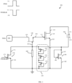
- FIG. 1 is a circuit diagram illustrating an embodiment of a circuit 100 for controlling the slew rate (i.e., dVout/dt) of a high voltage, enhancement mode, III-V semiconductor transistor, such as a high voltage enhancement mode GaN-based HEMT or MISHEMT or other III-V semiconductor-based HEMT or MISHEMT, during switching of the transistor specifically to an on state from an off-state.
- a high voltage, enhancement mode, III-V semiconductor transistor such as a high voltage enhancement mode GaN-based HEMT or MISHEMT or other III-V semiconductor-based HEMT or MISHEMT
- the circuit 100 can include an input/output pad 101 (also referred to herein as a pad or gate pad).
- the pad 101 can receive a gate control signal.
- the gate control signal can, for example, be a pulse-width modulation (PWM) signal, which oscillates between a low voltage (e.g., 0V or some other suitable low voltage) and a high voltage (e.g., 7V or some other suitable high voltage).
- PWM pulse-width modulation
- the circuit 100 can include a first transistor 110.
- the first transistor 110 can include a first source region 112 electrically connected to ground, a first drain region 113, a first channel region between the first source region 112 and the first drain region 113, and a first gate 111 adjacent to the first channel region.
- This first transistor 110 can be, for example, a high voltage, N-channel, enhancement mode III-V semiconductor transistor (e.g., a GaN-based HEMT or MISHEMT or some other III-V semiconductor-based HEMT or MISHEMT).
- the description of the first transistor 110 and any other transistor discussed herein as being an enhancement mode device refers to the fact that the transistor is normally in an off state and that application of a positive gate voltage to the gate thereof is required to switch the transistor to the on state (i.e., the conductive state).
- the circuit 100 can further include a second transistor 120.
- the second transistor 120 can include a second source region 122 electrically connected to the first gate 111 of the first transistor 110, a second drain region 123 electrically connected to the pad 101, a second channel region between the second source region 122 and the second drain region 123, and a second gate 121 adjacent to the second channel region.
- This second transistor 120 can be, for example, a low-voltage, N-channel, depletion mode device.
- the second transistor 120 can be a III-V semiconductor transistor (e.g., a GaN-based HEMT or MISHEMT or other III-V semiconductor HEMT or MISHEMT).
- the second transistor 120 could be a different type of transistor (e.g., a complementary metal oxide semiconductor (CMOS) transistor, a bipolar junction transistor (BJT), etc. if such devices are integrated on the same chip with III-V semiconductor devices).
- CMOS complementary metal oxide semiconductor
- BJT bipolar junction transistor
- various low voltage, N-channel, depletion mode device configurations are well known in the art and, thus, the details thereof have been omitted from this specification in order to allow the reader to focus on the salient aspects of the disclosed embodiments.
- the description of the second transistor 120 and any other transistor discussed herein as being a depletion mode device refers to the fact that the transistor is normally in an on state (i.e., a conductive state) and that application of a ground or negative gate voltage is required to switch the transistor to the off state. As discussed in greater detail below with regard to circuit 100 operation, this second transistor 120 allows impedance to be inserted between the pad 101 and the first gate 111 of the first transistor 110 in order to slow a voltage rise on the first gate 111 when necessary.
- the circuit 100 can further include a capacitor 130.
- the capacitor 130 can be, for example, a high voltage metal-oxide-metal (MOM) capacitor or some other suitable high voltage capacitor.
- the capacitor 130 can have a first conductive plate 131, a second conductive plate 132 opposite and essentially parallel to the first conductive plate 131, and a dielectric layer between the two plates 131-132.
- the first conductive plate 131 can be electrically connected to the first drain region 113 of the first transistor and the second conductive plate 132 can be electrically connected to the second gate 121 of the second transistor 120.
- the circuit 100 can further include a third transistor 170, a resistor 160, a voltage clamp 150, and a fourth transistor 140 connected in parallel between the second gate 121 of the second transistor 120 and ground. More specifically, the third transistor 170 can have a third source region 172 electrically connected to ground, a third drain region 173 electrically connected to the second gate 121 of the second transistor 120, a third channel region between the third source region and the third drain region, and a third gate 171 adjacent to the third channel region.
- the third gate 171 can be controlled by an inverted pulse-width modulation signal (PWMBAR) (i.e., another gate control signal that is inverted with respect to PWM).
- PWMBAR pulse-width modulation signal
- the resistor 160 can be, for example, a resistor derived from two-dimensional electron gas layer in an aluminum gallium nitride (AlGaN)/GaN heterostructure.
- the resistor 160 could be any other suitable resistor, such as a tantalum nitride (TaN) resistor, a silicon chromium (SiCr) resistor, or a polysilicon resistor.
- the fourth transistor 140 can have a fourth source region 142 electrically connected to ground, a fourth drain region 143 electrically connected to the second gate 121 of the second transistor 120, a fourth channel region between the fourth source region and the fourth drain region, and a fourth gate 141 adjacent to the fourth channel region and also electrically connected to the fourth drain region 143.
- the third transistor 170 and the fourth transistor 140 can both be, for example, N-channel, enhancement mode devices (i.e., normally in an off state as discussed above).
- the third transistor 170 and the fourth transistor 140 can be III-V semiconductor transistors (e.g., GaN-based HEMTs and/or MISHEMTs or other III-V semiconductor-based HEMTs and/or MISHEMTs). In other embodiments, they could be some different type of transistor (e.g., CMOS transistors, BJTs, etc. if such devices are integrated on the same chip with III-V semiconductor devices).
- the voltage clamp 150 can be a negative voltage clamp.
- the negative voltage clamp can include two or more stacked N-channel enhancement mode transistors (e.g., see transistors 151-153) with the drain region of the bottom transistor 153 in the stack being connected to ground and the source region of the top transistor 151 in the stack being connected to the second gate 121 of the second transistor 120 and with the gates of each transistor in the stack being tied to their respective drain regions.
- transistors 151-153 stacked N-channel enhancement mode transistors
- the second transistor 120 allows impedance to be inserted between the pad 101 and the first gate 111 of the first transistor 110 in order to allow the voltage rise on the first gate 111 to be slowed down during switching of the first transistor 110 to the on state when necessary. That is, instead of applying PWM directly to the first gate 111 so that the voltage rise on the first gate 111 corresponds to the rise time of PWM from low to high and is, thus, very quick when the first transistor 110 switches to the on state, impedance created by the second transistor 120 can be employed to slow down the voltage rise, for example, when dV/dt begins to happen. Specifically, an operation can start with the first transistor 110 in an off state, PWM low, and PWMBAR high.
- the second transistor 120 When PWM switches from low to high, the second transistor 120 will be in an on-state (i.e., conductive) and will pull up the gate voltage on the first gate 111 of the first transistor 110 and, thereby switch the first transistor 110 to the on-state. Initially, when the first transistor 110 switches to the on state, there will be a negative dVout/dt on the first drain region 113 of the first transistor 110. This will couple through capacitor 130 and resistor 160 (which, in combination, form a high pass filter) to the second gate 121 of the second transistor 120, thereby pulling the gate voltage on the second gate 121 of the second transistor 120 down below ground.
- capacitor 130 and resistor 160 which, in combination, form a high pass filter
- This will, in turn, debias the second transistor 120 and, thus, increase the impedance in series between the pad 101 and the first gate 111 of the first transistor 110.
- the increase in impedance between the pad 101 and the first gate 111 of the first transistor 110 effectively slows down the dVout/dt in a negative feedback loop.
- the negative feedback loop stabilizes to establish a slower dVout/dt until the first drain region 113 of the first transistor 110 completely switches, after which the second transistor 120 will once again fully turn on.
- the negative voltage clamp 150 is configured to prevent the gate voltage on the first gate 111 from ever dropping too far below ground and the fourth transistor 140 is configured to prevent the second gate 121 of the second transistor 120 from jumping up during positive dVout/dt.
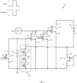
- FIG. 2 is a circuit diagram illustrating an embodiment of a circuit 200 for controlling the slew rate (i.e., dVout/dt) of a high voltage enhancement mode III-V semiconductor transistor, such as a high voltage enhancement mode GaN-based HEMT or MISHEMT or other III-V semiconductor-based HEMT or MISHEMT, during switching of the transistor specifically to an off state from an on-state.
- a high voltage enhancement mode III-V semiconductor transistor such as a high voltage enhancement mode GaN-based HEMT or MISHEMT or other III-V semiconductor-based HEMT or MISHEMT
- the circuit 200 can include an input/output pad 201 (also referred to herein as a pad or gate pad).
- the pad 201 can receive a gate control signal.
- the gate control signal can, for example, be a pulse-width modulation (PWM) signal, which oscillates between a low voltage (e.g., 0V or some other suitable low voltage) and a high voltage (e.g., 7V or some other suitable high voltage).
- PWM pulse-width modulation
- the circuit 200 can include a first transistor 210.
- the first transistor 210 can include a first source region 212 electrically connected to ground, a first drain region 213, a first channel region between the first source region 212 and the first drain region 213, and a first gate 211 adjacent to the first channel region.
- This first transistor 210 can be, for example, a high voltage, N-type, enhancement mode III-V semiconductor transistor (e.g., a GaN-based HEMT or MISHEMT or some other III-V semiconductor-based HEMT or MISHEMT).
- a high voltage, N-type, enhancement mode III-V semiconductor transistor e.g., a GaN-based HEMT or MISHEMT or some other III-V semiconductor-based HEMT or MISHEMT.
- the circuit 200 can further include a second transistor 220.
- the second transistor 220 can include a second source region 222 electrically connected to ground, a second drain region 223 electrically connected to a node between the pad 201 and the first gate 211 of the first transistor 210, a second channel region between the second source region 222 and the second drain region 223, and a second gate 221 adjacent to the second channel region.
- This second transistor 220 can be, for example, a low-voltage, N-channel, enhancement mode device.
- the second transistor 220 can be a III-V semiconductor transistor (e.g., GaN-based HEMT or MISHEMT or other III-V semiconductor-based HEMT or MISHEMT).
- the second transistor 220 could be a different type of transistor (e.g., a complementary metal oxide semiconductor (CMOS) transistor, a bipolar junction transistor (BJT), etc. if such devices are integrated on the same chip with III-V semiconductor devices).
- CMOS complementary metal oxide semiconductor
- BJT bipolar junction transistor
- various low voltage, N-channel, enhancement mode device configurations are well known in the art and, thus, the details thereof have been omitted from this specification in order to allow the reader to focus on the salient aspects of the disclosed embodiments.
- the circuit 200 can further include a capacitor 230.
- the capacitor 230 can be, for example, a high voltage metal-oxide-metal (MOM) capacitor or some other suitable high voltage capacitor.
- the capacitor 230 can have a first conductive plate 231, a second conductive plate 232, and a dielectric layer between the two plates 231-232.
- the first conductive plate 231 can be electrically connected to the first drain region 213 of the first transistor 210 and the second conductive plate 232 can be electrically connected to the second gate 221 of the second transistor 220.
- the circuit 200 can further include a third transistor 270, a resistor 260, a voltage clamp 250, and a fourth transistor 240 connected in parallel between the second gate 221 of the second transistor 220 and ground.
- the circuit 200 can further include a fifth transistor 280 connected in parallel with the second transistor between the first gate 211 of the first transistor 210 and ground.
- the third transistor 270 can have a third source region 272 electrically connected to ground, a third drain region 273 electrically connected to the second gate 221 of the second transistor 220, a third channel region between the third source region and the third drain region, and a third gate 271 adjacent to the third channel region.
- the third gate 271 can be controlled by PWM (i.e., the same signal received at pad 201).
- the resistor 260 can be, for example, a resistor derived from two-dimensional electron gas layer in an AlGaN/GaN heterostructure.
- the resistor 160 could be any other suitable resistor, such as a tantalum nitride (TaN) resistor, a silicon chromium (SiCr) resistor, or a polysilicon resistor.
- the fourth transistor 240 can have a fourth source region 242 electrically connected to the second gate 221, a fourth drain region 243 electrically connected to ground, a fourth channel region between the fourth source region and the fourth drain region, and a fourth gate 241 adjacent to the fourth channel region and also electrically connected to the fourth drain region 243.
- the fifth transistor 280 can include a fifth source region 282 connected to ground, a fifth drain region 283 connected to the first gate 211, a fifth channel region between the fifth source region and the fifth drain region, and a fifth gate 281 adjacent to the fifth channel region controlled by PWMBAR.
- the third transistor 270, the fourth transistor 240, and the fifth transistor 280 can be, for example, N-channel, enhancement mode devices (i.e., normally in an off state as discussed above). In some embodiments, they can be III-V semiconductor transistors (e.g., GaN-based HEMTs and/or MISHEMTs or other III-V semiconductor-based HEMTs and/or MISHEMTs).
- the voltage clamp 250 can be a positive voltage clamp.
- the positive voltage clamp can include two or more stacked N-channel enhancement mode transistors (e.g., see transistors 251-253) with the source region of the bottom transistor 253 in the stack being connected to ground and the drain region of the top transistor 251 in the stack being connected to the second gate 221 of the second transistor 220 and with the gates of each transistor in the stack being tied to their respective drain regions.
- the second transistor 220 allows a node between the pad 201 and the first gate 211 of the first transistor 210 to be pulled down in order to slow down positive dVout/dt on the first drain region 213 of the first transistor 210 during switching of the first transistor 210 to the off state when necessary.
- an operation can start with the first transistor 210 in an on state, with PWM high and PWMBAR low.
- the fifth transistor 280 also referred to herein as the primary pull-down transistor
- the primary pull-down transistor will switch to an on state and, thereby pulling down the gate voltage on the first gate 211 of the first transistor 210.
- the first transistor 210 will start to switch to the off state, thereby creating a positive dVout/dt on the first drain region 213.
- This positive dVout/dt will couple through the capacitor 230 and resistor 260 (which, in combination, form a high pass filter network) to the second gate 221 of the second transistor 220.
- the high pass filter network will raise the gate voltage on the second gate 221 to turn on the second transistor 220 (also referred to herein as the secondary or auxiliary pull-down transistor).
- the second transistor 220 turns on, there will be additional pulldown on the first gate 211 of the first transistor 210 that will further slow down the positive dVout/dt on the first drain region 213 in a negative feedback loop.
- FIG. 3 is a circuit diagram illustrating an embodiment of a circuit 300 for controlling the slew rate (i.e., dVout/dt) of a high voltage depletion mode III-V semiconductor transistor, such as a high voltage depletion mode GaN-based HEMT or MISHEMT or other III-V semiconductor-based HEMT or MISHEMT, during switching of the transistor specifically to an on state from an off state.
- a high voltage depletion mode III-V semiconductor transistor such as a high voltage depletion mode GaN-based HEMT or MISHEMT or other III-V semiconductor-based HEMT or MISHEMT
- the circuit 300 can include an input/output pad 301 (also referred to herein as a pad or gate pad).
- the pad 301 can receive a gate control signal.
- the gate control signal can, for example, be a pulse-width modulation (PWM) signal, which oscillates between a low voltage (e.g., 0V or some other suitable low voltage) and a high voltage (e.g., 7V or some other suitable high voltage).
- PWM pulse-width modulation
- the circuit 300 can include a first transistor 310.
- the first transistor 310 can include a first source region 312 electrically connected to ground, a first drain region 313, a first channel region between the first source region 312 and the first drain region 313, and a first gate 311 adjacent to the first channel region.
- This first transistor 310 can be, for example, a high voltage, N-channel, depletion mode III-V semiconductor transistor (e.g., a GaN-based HEMT or MISHEMT or some other III-V semiconductor-based HEMT or MISHEMT).
- the circuit 300 can further include a second transistor 320.
- the second transistor 320 can include a second source region 322 electrically connected to ground, a second drain region 323 electrically connected to a node between the pad 301 and the first gate 311 of the first transistor 310, a second channel region between the second source region 322 and the second drain region 323, and a second gate 321 adjacent to the second channel region.
- This second transistor 320 can be, for example, a low-voltage, N-channel, depletion mode device.
- the second transistor 320 can be a III-V semiconductor transistor (e.g., a GaN-based HEMT or MISHEMT or other III-V semiconductor-based HEMT or MISHEMT).
- the second transistor 320 could be a different type of transistor (e.g., a complementary metal oxide semiconductor (CMOS) transistor, a bipolar junction transistor (BJT), etc. if such devices are integrated on the same chip with III-V semiconductor devices).
- CMOS complementary metal oxide semiconductor
- BJT bipolar junction transistor
- various low voltage, N-channel, depletion mode device configurations are well known in the art and, thus, the details thereof have been omitted from this specification in order to allow the reader to focus on the salient aspects of the disclosed embodiments.
- the circuit 300 can further include a capacitor 330.
- the capacitor 330 can be, for example, a high voltage metal-oxide-metal (MOM) capacitor or some other suitable high voltage capacitor.
- the capacitor 330 can have a first conductive plate 331, a second conductive plate 332, and a dielectric layer between the two plates 331-332.
- the first conductive plate 331 can be electrically connected to the first drain region 313 of the first transistor 310 and the second conductive plate 332 can be electrically connected to the second gate 321 of the second transistor 320.
- the circuit 300 can further include a third transistor 370, a resistor 360, and a voltage clamp 350 connected in parallel between the second gate 321 of the second transistor 320 and ground.
- the circuit 300 can further include a fourth transistor 340 connected in series between the first transistor 310 and ground.
- the third transistor 370 can have a third source region 372 electrically connected to ground, a third drain region 373 electrically connected to the second gate 321 of the second transistor 320, a third channel region between the third source region and the third drain region, and a third gate 371 adjacent to the third channel region.
- the third gate 371 can be controlled by PWMBAR (i.e., an inverted gate control signal with respect to the gate control signal received at pad 301).
- the resistor 360 can be, for example, a resistor derived from two-dimensional electron gas layer in an AlGaN/GaN heterostructure.
- the resistor 160 could be any other suitable resistor, such as a tantalum nitride (TaN) resistor, a silicon chromium (SiCr) resistor, or a polysilicon resistor.
- the fourth transistor 340 can have a fourth source region 342 electrically connected to ground, a fourth drain region 343 electrically connected to the first source region 312 of the first transistor 310, a fourth channel region between the fourth drain region and the fourth source region, and a fourth gate 341 controlled by PWM.
- the third transistor 370 and the fourth transistor 340 can be, for example, N-channel, enhancement mode devices (i.e., normally in an off state as discussed above).
- they can be GaN-based HEMTs and/or MISHEMTs or other III-V semiconductor-based HEMTs and/or MISHEMTs.
- they could be some different type of transistor (e.g., CMOS transistors, BJTs, etc. if such devices are integrated on the same chip with GaN-based devices).
- the voltage clamp 350 can be a positive voltage clamp.
- the positive voltage clamp can include two or more stacked N-channel enhancement mode transistors (e.g., see transistors 351-353) with the source region of the bottom transistor 353 in the stack being connected to ground and the drain region of the top transistor 351 in the stack being connected to both the second gate 321 of the second transistor 320 and the second conductive plate 332 of the capacitor 330 and with the gates of each transistor in the stack being tied to their respective drain regions.
- the second transistor 320 allows a node between the pad 301 and the first gate 311 of the first transistor 310 to be pulled down in order to slow down negative dVout/dt on the first drain region 313 of the first transistor 310 during switching of the first transistor 310 to the on state when necessary.
- an operation can start with the first transistor 310 in an off state, with PWM low and PWMBAR high.
- PWMBAR high the third transistor 370 will be on and will pull down the gate voltage on the second gate 321 of the second transistor 320. Since the gate voltage on the second gate 321 of the second transistor 320 is held low, it will be fully turned on because, as mentioned above, the second transistor 320 is specifically a depletion mode device in this embodiment.
- the second source region 322 of the second transistor 320 will also be low, as it is connected to ground. As a result, the second transistor provides a low impedance path from the first gate 311 of the first transistor 310 to ground.
- the first source region 312 of the first transistor 310 will be at the pinch off voltage (Vpinch) of the first transistor 310 because, as mentioned above, the first transistor 310 is also a depletion mode device in this embodiment.
- the fourth transistor 340 will turn on, thereby pulling down the source voltage on the first source region 312 of the first transistor 310 to ground.
- the first gate 311 is already at ground and, thus, the first transistor 310 (which as mentioned above is a depletion mode device) will turn on causing a negative dVout/dt.
- This negative dVout/dt will couple through the capacitor 330 and resistor 360 (which, in combination, form a high pass filter network) and will pull down the gate voltage on the second gate 321 of the second transistor 320 (i.e., the other depletion mode device) below the source voltage thereof so as to increase its impedance.
- the Miller capacitance (Cgd) of the first transistor 310 i.e., the intrinsic capacitance between the first drain region 313 and the first gate 311 of the first transistor 310 will push the gate voltage on the first gate 311 below ground, thereby slowing down the negative dVout/dt.
- a negative feedback loop will be established to setup a dVout/dt and this effect will stop once the dVout/dt is completed.
- a semiconductor material refers to a material whose conducting properties can be altered by doping with an impurity.
- semiconductor materials include, for example, silicon-based semiconductor materials (e.g., silicon, silicon germanium, silicon germanium carbide, silicon carbide, etc.) and III-V semiconductor materials (also referred to as III-V compound semiconductors), which are compounds obtained by combining group III elements, such as aluminum (Al), gallium (Ga), or indium (In), with group V elements, such as nitrogen (N), phosphorous (P), arsenic (As) or antimony (Sb)) (e.g., GaN, InP, GaAs, or GaP).
- group III elements such as aluminum (Al), gallium (Ga), or indium (In)
- group V elements such as nitrogen (N), phosphorous (P), arsenic (As) or antimony (Sb)
- a pure semiconductor material and, more particularly, a semiconductor material that is not doped with an impurity for the purposes of increasing conductivity is referred to in the art as an intrinsic semiconductor.
- a semiconductor material that is doped with an impurity for the purposes of increasing conductivity is referred to in the art as an extrinsic semiconductor and will be more conductive than an intrinsic semiconductor made of the same base material. That is, extrinsic silicon will be more conductive than intrinsic silicon; extrinsic silicon germanium will be more conductive than intrinsic silicon germanium; and so on.
- a silicon-based semiconductor material e.g., silicon, silicon germanium, etc.
- a Group III dopant such as boron (B) or indium (In)
- a silicon-based semiconductor material is typically doped a Group V dopant, such as arsenic (As), phosphorous (P) or antimony (Sb), to achieve N-type conductivity.
- a gallium nitride (GaN)-based semiconductor material is typically doped with magnesium (Mg) to achieve P-type conductivity and with silicon (Si) or oxygen to achieve N-type conductivity.
- Mg magnesium
- Si silicon
- oxygen oxygen
- different conductivity levels will depend upon the relative concentration levels of the dopant(s) in a given semiconductor region.
- a semiconductor region or layer is described as being at a higher conductivity level than another semiconductor region or layer, it is more conductive (less resistive) than the other semiconductor region or layer; whereas, when a semiconductor region or layer is described as being at a lower conductivity level than another semiconductor region or layer, it is less conductive (more resistive) than that other semiconductor region or layer.
- laterally is used herein to describe the relative locations of elements and, more particularly, to indicate that an element is positioned to the side of another element as opposed to above or below the other element, as those elements are oriented and illustrated in the drawings.
- an element that is positioned laterally adjacent to another element will be beside the other element
- an element that is positioned laterally immediately adjacent to another element will be directly beside the other element
- an element that laterally surrounds another element will be adjacent to and border the outer sidewalls of the other element.
- the term "include” and its variants may be interpreted as meaning that an embodiment includes stated features, while not necessarily excluding the presence of other features that are not explicitly stated.
Landscapes
- Physics & Mathematics (AREA)
- Nonlinear Science (AREA)
- Junction Field-Effect Transistors (AREA)
- Electronic Switches (AREA)
Applications Claiming Priority (1)
| Application Number | Priority Date | Filing Date | Title |
|---|---|---|---|
| US18/045,909 US12143112B2 (en) | 2022-10-12 | 2022-10-12 | Circuit for controlling the slew rate of a transistor |
Publications (2)
| Publication Number | Publication Date |
|---|---|
| EP4354733A2 true EP4354733A2 (de) | 2024-04-17 |
| EP4354733A3 EP4354733A3 (de) | 2024-05-29 |
Family
ID=88016356
Family Applications (1)
| Application Number | Title | Priority Date | Filing Date |
|---|---|---|---|
| EP23196216.8A Pending EP4354733A3 (de) | 2022-10-12 | 2023-09-08 | Schaltung zur steuerung der anstiegsgeschwindigkeit eines transistors |
Country Status (3)
| Country | Link |
|---|---|
| US (1) | US12143112B2 (de) |
| EP (1) | EP4354733A3 (de) |
| CN (1) | CN117879555A (de) |
Families Citing this family (1)
| Publication number | Priority date | Publication date | Assignee | Title |
|---|---|---|---|---|
| US12323143B2 (en) * | 2023-02-10 | 2025-06-03 | Globalfoundries U.S. Inc. | Charge pumps, logic circuits including charge pumps, logic devices including logic circuits, and methods of operating logic circuits |
Family Cites Families (13)
| Publication number | Priority date | Publication date | Assignee | Title |
|---|---|---|---|---|
| JPH10261925A (ja) | 1997-03-17 | 1998-09-29 | Toshiba Corp | 高周波増幅器 |
| DE19902520B4 (de) | 1999-01-22 | 2005-10-06 | Siemens Ag | Hybrid-Leistungs-MOSFET |
| JP2003243512A (ja) | 2002-02-14 | 2003-08-29 | Hitachi Ltd | 静電破壊保護回路 |
| US8624662B2 (en) | 2010-02-05 | 2014-01-07 | Transphorm Inc. | Semiconductor electronic components and circuits |
| US8804290B2 (en) * | 2012-01-17 | 2014-08-12 | Texas Instruments Incorporated | Electrostatic discharge protection circuit having buffer stage FET with thicker gate oxide than common-source FET |
| US9035690B2 (en) | 2012-08-30 | 2015-05-19 | Infineon Technologies Dresden Gmbh | Circuit arrangement with a first semiconductor device and with a plurality of second semiconductor devices |
| US9692408B2 (en) | 2012-12-21 | 2017-06-27 | Gan Systems Inc. | Devices and systems comprising drivers for power conversion circuits |
| US9929652B1 (en) | 2015-12-08 | 2018-03-27 | Navitas Semiconductor, Inc. | GaN FET with integrated driver and slew rate control |
| EP3440696B1 (de) | 2016-04-08 | 2021-06-09 | Power Integrations, Inc. | Integrierter widerstand für halbleiterbauelement |
| KR102674752B1 (ko) | 2018-09-05 | 2024-06-14 | 이피션트 파워 컨버젼 코퍼레이션 | GaN 기반 조정 가능한 전류 드라이버 회로 |
| US11189717B2 (en) * | 2019-01-10 | 2021-11-30 | Arizona Board Of Regents On Behalf Of Arizona State University | Steep slope transistors with threshold switching devices |
| TWI726817B (zh) * | 2020-09-24 | 2021-05-01 | 漢威光電股份有限公司 | 靜電放電保護電路 |
| US11929012B2 (en) * | 2021-02-22 | 2024-03-12 | Samsung Electronics Co., Ltd. | Display module and display apparatus having the same |
-
2022
- 2022-10-12 US US18/045,909 patent/US12143112B2/en active Active
-
2023
- 2023-09-08 EP EP23196216.8A patent/EP4354733A3/de active Pending
- 2023-09-12 CN CN202311169271.5A patent/CN117879555A/zh active Pending
Also Published As
| Publication number | Publication date |
|---|---|
| EP4354733A3 (de) | 2024-05-29 |
| US12143112B2 (en) | 2024-11-12 |
| US20240128958A1 (en) | 2024-04-18 |
| CN117879555A (zh) | 2024-04-12 |
Similar Documents
| Publication | Publication Date | Title |
|---|---|---|
| US11955478B2 (en) | Power semiconductor device with an auxiliary gate structure | |
| US11336279B2 (en) | Power semiconductor device with a series connection of two devices | |
| TWI839514B (zh) | 具有輔助閘極結構之功率半導體裝置 | |
| CN109427772B (zh) | 用于衬底电位稳定化的具有无源电网络的双向开关 | |
| TWI499058B (zh) | 氮化鎵二極體及積體組件 | |
| EP3696980A2 (de) | Konfigurationen von verbundbauelementen mit einem normal-an und einem normal-aus fet | |
| US12382651B2 (en) | Power semiconductor device with an auxiliary gate structure | |
| US11594628B2 (en) | Monolithic microwave integrated circuits having both enhancement-mode and depletion mode transistors | |
| US9300223B2 (en) | Rectifying circuit and semiconductor device | |
| US11139292B2 (en) | Conductivity modulated drain extended MOSFET | |
| US12575125B2 (en) | Field effect transistor with selective modified access regions | |
| US20140319532A1 (en) | Heterojunction Semiconductor Device and Manufacturing Method | |
| EP4354733A2 (de) | Schaltung zur steuerung der anstiegsgeschwindigkeit eines transistors | |
| US10128829B2 (en) | Composite semiconductor device | |
| US11869964B2 (en) | Field effect transistors with modified access regions | |
| US12294364B2 (en) | Transistor with integrated turn-off slew rate control | |
| CN113809067B (zh) | 一种带有片内栅极回跳保护的常关型hemt器件 | |
| JP7770424B2 (ja) | 修正アクセス領域を備える電界効果トランジスタ | |
| TW202541617A (zh) | 功率電晶體、高電子遷移率電晶體及包括高電子遷移率電晶體的器件 | |
| CN121420472A (zh) | 半导体开关 |
Legal Events
| Date | Code | Title | Description |
|---|---|---|---|
| PUAI | Public reference made under article 153(3) epc to a published international application that has entered the european phase |
Free format text: ORIGINAL CODE: 0009012 |
|
| STAA | Information on the status of an ep patent application or granted ep patent |
Free format text: STATUS: REQUEST FOR EXAMINATION WAS MADE |
|
| 17P | Request for examination filed |
Effective date: 20230908 |
|
| AK | Designated contracting states |
Kind code of ref document: A2 Designated state(s): AL AT BE BG CH CY CZ DE DK EE ES FI FR GB GR HR HU IE IS IT LI LT LU LV MC ME MK MT NL NO PL PT RO RS SE SI SK SM TR |
|
| PUAL | Search report despatched |
Free format text: ORIGINAL CODE: 0009013 |
|
| AK | Designated contracting states |
Kind code of ref document: A3 Designated state(s): AL AT BE BG CH CY CZ DE DK EE ES FI FR GB GR HR HU IE IS IT LI LT LU LV MC ME MK MT NL NO PL PT RO RS SE SI SK SM TR |
|
| RIC1 | Information provided on ipc code assigned before grant |
Ipc: H03K 17/687 20060101ALI20240422BHEP Ipc: H03K 17/16 20060101AFI20240422BHEP |
|
| GRAP | Despatch of communication of intention to grant a patent |
Free format text: ORIGINAL CODE: EPIDOSNIGR1 |
|
| STAA | Information on the status of an ep patent application or granted ep patent |
Free format text: STATUS: GRANT OF PATENT IS INTENDED |
|
| INTG | Intention to grant announced |
Effective date: 20260224 |