EP4354443A2 - Kalibrierungsverfahren und -strukturen für partitionierte speicherarchitektur mit einzelwiderstand oder doppelwiderstandspeicherelementen - Google Patents
Kalibrierungsverfahren und -strukturen für partitionierte speicherarchitektur mit einzelwiderstand oder doppelwiderstandspeicherelementen Download PDFInfo
- Publication number
- EP4354443A2 EP4354443A2 EP23187997.4A EP23187997A EP4354443A2 EP 4354443 A2 EP4354443 A2 EP 4354443A2 EP 23187997 A EP23187997 A EP 23187997A EP 4354443 A2 EP4354443 A2 EP 4354443A2
- Authority
- EP
- European Patent Office
- Prior art keywords
- calibration
- memory
- resistor
- specific
- column
- Prior art date
- Legal status (The legal status is an assumption and is not a legal conclusion. Google has not performed a legal analysis and makes no representation as to the accuracy of the status listed.)
- Pending
Links
Images


Classifications
-
- G—PHYSICS
- G11—INFORMATION STORAGE
- G11C—STATIC STORES
- G11C7/00—Arrangements for writing information into, or reading information out from, a digital store
- G11C7/10—Input/output [I/O] data interface arrangements, e.g. I/O data control circuits, I/O data buffers
- G11C7/1015—Read-write modes for single port memories, i.e. having either a random port or a serial port
- G11C7/1039—Read-write modes for single port memories, i.e. having either a random port or a serial port using pipelining techniques, i.e. using latches between functional memory parts, e.g. row/column decoders, I/O buffers, sense amplifiers
-
- G—PHYSICS
- G11—INFORMATION STORAGE
- G11C—STATIC STORES
- G11C29/00—Checking stores for correct operation ; Subsequent repair; Testing stores during standby or offline operation
- G11C29/02—Detection or location of defective auxiliary circuits, e.g. defective refresh counters
- G11C29/028—Detection or location of defective auxiliary circuits, e.g. defective refresh counters with adaption or trimming of parameters
-
- G—PHYSICS
- G06—COMPUTING OR CALCULATING; COUNTING
- G06F—ELECTRIC DIGITAL DATA PROCESSING
- G06F15/00—Digital computers in general; Data processing equipment in general
- G06F15/76—Architectures of general purpose stored program computers
- G06F15/78—Architectures of general purpose stored program computers comprising a single central processing unit
- G06F15/7807—System on chip, i.e. computer system on a single chip; System in package, i.e. computer system on one or more chips in a single package
- G06F15/7821—Tightly coupled to memory, e.g. computational memory, smart memory, processor in memory
-
- G—PHYSICS
- G06—COMPUTING OR CALCULATING; COUNTING
- G06N—COMPUTING ARRANGEMENTS BASED ON SPECIFIC COMPUTATIONAL MODELS
- G06N3/00—Computing arrangements based on biological models
- G06N3/02—Neural networks
- G06N3/06—Physical realisation, i.e. hardware implementation of neural networks, neurons or parts of neurons
- G06N3/063—Physical realisation, i.e. hardware implementation of neural networks, neurons or parts of neurons using electronic means
- G06N3/065—Analogue means
-
- G—PHYSICS
- G11—INFORMATION STORAGE
- G11C—STATIC STORES
- G11C11/00—Digital stores characterised by the use of particular electric or magnetic storage elements; Storage elements therefor
- G11C11/02—Digital stores characterised by the use of particular electric or magnetic storage elements; Storage elements therefor using magnetic elements
- G11C11/16—Digital stores characterised by the use of particular electric or magnetic storage elements; Storage elements therefor using magnetic elements using elements in which the storage effect is based on magnetic spin effect
- G11C11/165—Auxiliary circuits
- G11C11/1653—Address circuits or decoders
- G11C11/1655—Bit-line or column circuits
-
- G—PHYSICS
- G11—INFORMATION STORAGE
- G11C—STATIC STORES
- G11C11/00—Digital stores characterised by the use of particular electric or magnetic storage elements; Storage elements therefor
- G11C11/02—Digital stores characterised by the use of particular electric or magnetic storage elements; Storage elements therefor using magnetic elements
- G11C11/16—Digital stores characterised by the use of particular electric or magnetic storage elements; Storage elements therefor using magnetic elements using elements in which the storage effect is based on magnetic spin effect
- G11C11/165—Auxiliary circuits
- G11C11/1673—Reading or sensing circuits or methods
-
- G—PHYSICS
- G11—INFORMATION STORAGE
- G11C—STATIC STORES
- G11C11/00—Digital stores characterised by the use of particular electric or magnetic storage elements; Storage elements therefor
- G11C11/02—Digital stores characterised by the use of particular electric or magnetic storage elements; Storage elements therefor using magnetic elements
- G11C11/16—Digital stores characterised by the use of particular electric or magnetic storage elements; Storage elements therefor using magnetic elements using elements in which the storage effect is based on magnetic spin effect
- G11C11/165—Auxiliary circuits
- G11C11/1675—Writing or programming circuits or methods
-
- G—PHYSICS
- G11—INFORMATION STORAGE
- G11C—STATIC STORES
- G11C11/00—Digital stores characterised by the use of particular electric or magnetic storage elements; Storage elements therefor
- G11C11/02—Digital stores characterised by the use of particular electric or magnetic storage elements; Storage elements therefor using magnetic elements
- G11C11/16—Digital stores characterised by the use of particular electric or magnetic storage elements; Storage elements therefor using magnetic elements using elements in which the storage effect is based on magnetic spin effect
- G11C11/165—Auxiliary circuits
- G11C11/1697—Power supply circuits
-
- G—PHYSICS
- G11—INFORMATION STORAGE
- G11C—STATIC STORES
- G11C11/00—Digital stores characterised by the use of particular electric or magnetic storage elements; Storage elements therefor
- G11C11/54—Digital stores characterised by the use of particular electric or magnetic storage elements; Storage elements therefor using elements simulating biological cells, e.g. neuron
-
- G—PHYSICS
- G11—INFORMATION STORAGE
- G11C—STATIC STORES
- G11C13/00—Digital stores characterised by the use of storage elements not covered by groups G11C11/00, G11C23/00, or G11C25/00
- G11C13/0002—Digital stores characterised by the use of storage elements not covered by groups G11C11/00, G11C23/00, or G11C25/00 using resistive RAM [RRAM] elements
- G11C13/0021—Auxiliary circuits
- G11C13/0023—Address circuits or decoders
- G11C13/0026—Bit-line or column circuits
-
- G—PHYSICS
- G11—INFORMATION STORAGE
- G11C—STATIC STORES
- G11C13/00—Digital stores characterised by the use of storage elements not covered by groups G11C11/00, G11C23/00, or G11C25/00
- G11C13/0002—Digital stores characterised by the use of storage elements not covered by groups G11C11/00, G11C23/00, or G11C25/00 using resistive RAM [RRAM] elements
- G11C13/0021—Auxiliary circuits
- G11C13/0038—Power supply circuits
-
- G—PHYSICS
- G11—INFORMATION STORAGE
- G11C—STATIC STORES
- G11C13/00—Digital stores characterised by the use of storage elements not covered by groups G11C11/00, G11C23/00, or G11C25/00
- G11C13/0002—Digital stores characterised by the use of storage elements not covered by groups G11C11/00, G11C23/00, or G11C25/00 using resistive RAM [RRAM] elements
- G11C13/0021—Auxiliary circuits
- G11C13/004—Reading or sensing circuits or methods
-
- G—PHYSICS
- G11—INFORMATION STORAGE
- G11C—STATIC STORES
- G11C13/00—Digital stores characterised by the use of storage elements not covered by groups G11C11/00, G11C23/00, or G11C25/00
- G11C13/0002—Digital stores characterised by the use of storage elements not covered by groups G11C11/00, G11C23/00, or G11C25/00 using resistive RAM [RRAM] elements
- G11C13/0021—Auxiliary circuits
- G11C13/0069—Writing or programming circuits or methods
-
- G—PHYSICS
- G11—INFORMATION STORAGE
- G11C—STATIC STORES
- G11C29/00—Checking stores for correct operation ; Subsequent repair; Testing stores during standby or offline operation
- G11C29/02—Detection or location of defective auxiliary circuits, e.g. defective refresh counters
- G11C29/022—Detection or location of defective auxiliary circuits, e.g. defective refresh counters in I/O circuitry
-
- G—PHYSICS
- G11—INFORMATION STORAGE
- G11C—STATIC STORES
- G11C29/00—Checking stores for correct operation ; Subsequent repair; Testing stores during standby or offline operation
- G11C29/04—Detection or location of defective memory elements, e.g. cell constructio details, timing of test signals
- G11C29/50—Marginal testing, e.g. race, voltage or current testing
-
- G—PHYSICS
- G11—INFORMATION STORAGE
- G11C—STATIC STORES
- G11C7/00—Arrangements for writing information into, or reading information out from, a digital store
- G11C7/10—Input/output [I/O] data interface arrangements, e.g. I/O data control circuits, I/O data buffers
- G11C7/1006—Data managing, e.g. manipulating data before writing or reading out, data bus switches or control circuits therefor
- G11C7/1012—Data reordering during input/output, e.g. crossbars, layers of multiplexers, shifting or rotating
-
- G—PHYSICS
- G11—INFORMATION STORAGE
- G11C—STATIC STORES
- G11C7/00—Arrangements for writing information into, or reading information out from, a digital store
- G11C7/12—Bit line control circuits, e.g. drivers, boosters, pull-up circuits, pull-down circuits, precharging circuits, equalising circuits, for bit lines
-
- G—PHYSICS
- G11—INFORMATION STORAGE
- G11C—STATIC STORES
- G11C11/00—Digital stores characterised by the use of particular electric or magnetic storage elements; Storage elements therefor
- G11C11/02—Digital stores characterised by the use of particular electric or magnetic storage elements; Storage elements therefor using magnetic elements
- G11C11/16—Digital stores characterised by the use of particular electric or magnetic storage elements; Storage elements therefor using magnetic elements using elements in which the storage effect is based on magnetic spin effect
- G11C11/161—Digital stores characterised by the use of particular electric or magnetic storage elements; Storage elements therefor using magnetic elements using elements in which the storage effect is based on magnetic spin effect details concerning the memory cell structure, e.g. the layers of the ferromagnetic memory cell
-
- G—PHYSICS
- G11—INFORMATION STORAGE
- G11C—STATIC STORES
- G11C13/00—Digital stores characterised by the use of storage elements not covered by groups G11C11/00, G11C23/00, or G11C25/00
- G11C13/0002—Digital stores characterised by the use of storage elements not covered by groups G11C11/00, G11C23/00, or G11C25/00 using resistive RAM [RRAM] elements
- G11C13/0004—Digital stores characterised by the use of storage elements not covered by groups G11C11/00, G11C23/00, or G11C25/00 using resistive RAM [RRAM] elements comprising amorphous/crystalline phase transition cells
-
- G—PHYSICS
- G11—INFORMATION STORAGE
- G11C—STATIC STORES
- G11C13/00—Digital stores characterised by the use of storage elements not covered by groups G11C11/00, G11C23/00, or G11C25/00
- G11C13/0002—Digital stores characterised by the use of storage elements not covered by groups G11C11/00, G11C23/00, or G11C25/00 using resistive RAM [RRAM] elements
- G11C13/0007—Digital stores characterised by the use of storage elements not covered by groups G11C11/00, G11C23/00, or G11C25/00 using resistive RAM [RRAM] elements comprising metal oxide memory material, e.g. perovskites
-
- G—PHYSICS
- G11—INFORMATION STORAGE
- G11C—STATIC STORES
- G11C13/00—Digital stores characterised by the use of storage elements not covered by groups G11C11/00, G11C23/00, or G11C25/00
- G11C13/0002—Digital stores characterised by the use of storage elements not covered by groups G11C11/00, G11C23/00, or G11C25/00 using resistive RAM [RRAM] elements
- G11C13/0009—RRAM elements whose operation depends upon chemical change
- G11C13/0011—RRAM elements whose operation depends upon chemical change comprising conductive bridging RAM [CBRAM] or programming metallization cells [PMCs]
-
- G—PHYSICS
- G11—INFORMATION STORAGE
- G11C—STATIC STORES
- G11C13/00—Digital stores characterised by the use of storage elements not covered by groups G11C11/00, G11C23/00, or G11C25/00
- G11C13/0002—Digital stores characterised by the use of storage elements not covered by groups G11C11/00, G11C23/00, or G11C25/00 using resistive RAM [RRAM] elements
- G11C13/0021—Auxiliary circuits
- G11C13/004—Reading or sensing circuits or methods
- G11C2013/0054—Read is performed on a reference element, e.g. cell, and the reference sensed value is used to compare the sensed value of the selected cell
Definitions
- the present invention relates to in-memory processing and, more particularly, to a memory architecture for in-memory processing and calibration thereof.
- NNs neural networks
- a NN is a deep learning algorithm where approximately 90% of the computations performed in the algorithm are multiply-and-accumulate (MAC) operations.
- MAC multiply-and-accumulate
- the various MAC operations are used to compute the products of inputs (also referred to as activations), which are identified intensity values of the pixels in a receptive field, and weights in a filter matrix (also referred to as a kernel) of the same size as the receptive field, and to further compute the sum of the products.
- a structure and, particularly, a partitioned memory architecture which includes single resistor or dual resistor memory elements, which is configured for in-memory pipeline processing with minimal local IR drops, and which further includes additional circuitry to facilitate calibration processing.
- the structure can include an array of memory banks arranged in rows and columns.
- Each memory bank can include input nodes, at least one bitline, and memory elements connected to the input nodes, respectively.
- Each memory element can include at least one programmable resistor connected between a corresponding input node and the at least one bitline.
- Each memory element can further include at least one feedback buffer circuit connected to the at least one bitline, respectively.
- each row of the memory banks in the array can include an initial memory bank (i.e., the first memory bank in the row) and each initial memory bank can include: amplifiers connected in series between the input nodes and the memory elements, respectively; track-and-hold devices; a calibration supply line; and multiplexors.
- Each multiplexor can include at least a first input connected to one of the track-and-hold devices and a second input connected to the calibration supply line.
- Each multiplexor can further have an output connected to one of the amplifiers.
- each multiplexor can selectively connect either a track-and-hold device (which provides a voltage input signal for use during in-memory pipeline processing) or the calibration supply line (which provides a calibration input voltage for use during calibration processing) to the input of an amplifier.
- the structure can include an array of memory banks arranged in rows and columns.
- Each memory bank can include both operational circuitry and calibration circuitry.
- Each memory bank can further include duplicate pairs of single resistor memory elements.
- Each duplicate pair of single resistor memory elements can include two single resistor memory elements, where each single resistor memory element includes a single programmable resistor.
- Each duplicate pair of single resistor memory elements can also include switches at the opposing end terminals of the programmable resistors therein.
- each programmable resistor of each single resistor memory element of each duplicate pair is connectable to (i.e., cable of being connected to) the operational circuitry, connectable to the calibration circuitry, and also disconnectable from (i.e., cable of being disconnected from) both the operational circuitry and the calibration circuitry.
- the switches can be controlled so as to connect one programmable resistor of one single resistor memory element of a duplicate pair to the operational circuitry for in-memory pipeline processing and so as to either connect the programmable resistor of the other single resistor memory element of the duplicate pair to the calibration circuitry for calibration processing or disconnect it from both the operational circuitry and the calibration circuitry (e.g., when no calibration processing is being performed or when calibration processing is directed to a different programmable resistor in the same column).
- the structure can similarly include an array of memory banks arranged in rows and columns.
- Each memory bank can include both operational circuitry and calibration circuitry.
- Each memory bank can further include duplicate pairs of dual resistor memory elements.
- Each duplicate pair of dual resistor memory elements can include two dual resistor memory elements, where each dual resistor memory element in the pair include both a first programmable resistor and a second programmable resistor.
- Each duplicate pair of dual resistor memory elements further includes switches at opposing end terminals of both programmable resistors of each dual resistor memory element. These switches are controllable so that each programmable resistor of each dual resistor memory element of each duplicate pair is connectable to the operational circuitry, connectable to the calibration circuitry, and also disconnectable from both the operational circuitry and the calibration circuitry.
- the switches can be controlled so as to connect the two programmable resistors of one dual resistor memory element of a duplicate pair to the operational circuitry for in-memory pipeline processing.
- the switches can further be controlled to connect one programmable resistor of the other dual resistor memory element of the duplicate pair to the calibration circuitry for calibration processing and to disconnect the other from the operational circuitry and the calibration circuit.
- the switches can further be controlled to disconnect both programmable resistors of the other dual resistor memory element of the duplicate pair from both the operational circuitry and the calibration circuitry (e.g., when no calibration processing is being performed or when calibration processing is directed to a different programmable resistor in the same column).
- a structure and, particularly, a partitioned memory architecture which includes single resistor or dual resistor memory elements, which is configured for in-memory pipeline processing (such as matrix vector multiplication processing, multiply-and-accumulate (MAC) processing, etc.) with minimal local IR drops, and which further includes additional circuitry to facilitate calibration processing.
- the additional circuitry enables calibration processing when in-memory pipeline processing is paused (i.e., the additional circuitry enables interspersed calibration processing).
- the same bitlines and data sensing elements used for in-memory pipeline processing are also used for calibration processing.
- the additional circuitry enables calibration processing concurrent with in-memory pipeline processing.
- the additional circuitry includes duplicate pairs of memory elements with programmable resistors that can be connected to the operational circuitry for in-memory processing, to the calibration circuitry (including calibration-specific sense lines and sensing elements) for calibration processing, or to neither such that one memory element of each duplicate pair always remains operational allowing the other to undergo calibration on demand.
- FIGs. 1 and 2 are schematic diagrams illustrating disclosed embodiments of a structure 100, 200, respectively, including a partitioned memory architecture configured to enable in-memory pipeline processing (e.g., MAC processing) to be paused for calibration processing.
- in-memory pipeline processing e.g., MAC processing
- the structure 100, 200 can include a partitioned array of memory elements 110, 210.
- the memory elements 110 are single resistor memory elements, whereas, in the structure 200, the memory elements are dual resistor memory elements.
- each memory element 110 can include a single programmable resistor 111 (also referred to herein as a variable resistor).
- each memory element 210 can include two programmable resistors and, particularly, a first programmable resistor 211 and a second programmable resistor 212.
- the first and second programmable resistors 211-212 can be essentially the same (i.e., can have the same design, be the same type, be made of the same materials, etc.).
- each programmable resistor in the memory element 110 of the structure 100 or the memory element 210 of the structure 200, can be any type of resistor having a controllable (i.e., adjustable) resistance and suitable for use as a non-volatile resistive memory element (i.e., a resistive memory element that retains its programmed resistance state even if/when the device loses power).
- each programmable resistor 111, 211-212 can be a resistive random access memory (RRAM)-type programmable resistor.
- each programmable resistor 111, 211-212 can be a phase change memory (PCM)-type programmable resistor, magnetic tunnel junction (MTJ)-type programmable resistor, or any other suitable type of programmable resistor configured so that, by applying specific bias conditions to one or both opposing end terminals of the resistor, the resistance of the programmable resistor can be changed between at least two different stable resistance states.
- PCM phase change memory
- MTJ magnetic tunnel junction
- the resistance states of such a programmable resistor can be programmed to a maximum resistance state, to a minimum resistance state, and optionally to one or more resistance states along a continuum between the minimum and maximum resistance states.
- the programmable resistors could have a significantly large number of different stable resistance states (e.g., 16 or more).
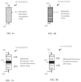
- FIGs. 3A-3D illustrate an RRAM-type programmable resistor that could be employed in a memory element 110, 210 as the programmable resistor(s) 111, 211-212.
- An RRAM is typically a back end of the line (BEOL) multi-layered structure, which includes two metallic layers 312 and 314 separated by a dielectric region 313 (also referred to herein as a resistance switching region).
- BEOL back end of the line
- metal ions migrate to: (a) grow conductive filament(s) 315 in the dielectric region 313 extending between the metallic layers 312 and 314 so that the resistance state of the RRAM-type programmable resistor decreases or (b) break down conductive filament(s) within the dielectric region 313 between the metallic layers 312 and 314 so that the resistance state of the RRAM-type programmable resistor increases.
- conductive filament(s) 315 in the dielectric region 313 extending between the metallic layers 312 and 314 so that the resistance state of the RRAM-type programmable resistor decreases
- break down conductive filament(s) within the dielectric region 313 between the metallic layers 312 and 314 so that the resistance state of the RRAM-type programmable resistor increases.
- An RRAM-type programmable resistor could include metallic layers 312-314 (e.g., of platinum (Pt), titanium (Ti), titanium nitride (TiN), etc.) and, between the metallic layers 212-214, a dielectric region 313 including an oxide layer, such as a tantalum oxide (Ta2O5) layer, a hafnium oxide (HfO2) layer, an iron oxide (Fe2O3) layer, a titanium oxide (TiO2) layer, etc.
- metallic layers 312-314 e.g., of platinum (Pt), titanium (Ti), titanium nitride (TiN), etc.
- a dielectric region 313 including an oxide layer, such as a tantalum oxide (Ta2O5) layer, a hafnium oxide (HfO2) layer, an iron oxide (Fe2O3) layer, a titanium oxide (TiO2) layer, etc.
- one or more thin interface barrier layers e.g., a second oxide layer, such as aluminum oxide (Al2O3) or some other oxide layer, an amorphous silicon layer, or some other suitable interface barrier layer
- a second oxide layer such as aluminum oxide (Al2O3) or some other oxide layer
- Al2O3 aluminum oxide
- amorphous silicon layer or some other suitable interface barrier layer
- FIGs. 4A-4B illustrate a PCM-type programmable resistor that could be employed in a memory element 110, 210 as the programmable resistor(s) 111, 211-212.
- a PCM-type programmable resistor includes a phase change material 411 (e.g., a chalcogenide compound) with programmable structural phases that exhibit different stable resistance states. For example, in a fully amorphous phase, exemplified by the drawing shown in FIG. 4A , the resistor will have the maximum resistance, whereas in a fully crystalline phase, exemplified by the drawing shown in FIG. 4B , the resistor will have the minimum resistance.
- phase change material 411 e.g., a chalcogenide compound
- the resistor will have a resistance between the maximum and the minimum resistances. Phase changes are dependent upon the local temperature of the PCM, which is controlled by the length and strength of an applied voltage.
- changing from a crystalline phase toward or to an amorphous phase can be achieved by applying a short high voltage pulse to one or both of the opposing end terminals 421-422 in order to quickly heat the phase change material above its melting point
- changing from an amorphous phase toward or to a crystalline phase can be achieved by applying a longer lower voltage pulse to one or both of the opposing terminals 421-422 in order to heat the phase change material to its crystallization temperature and then allowing it to cool.
- FIGs. 5A-5B illustrate an MTJ-type programmable resistor that could be employed in a memory element 110, 210 as the programmable resistor(s) 111, 211-212.
- An MTJ-type programmable resistor is typically a back end of the line (BEOL) multi-layered structure, which includes a free ferromagnetic layer 514 (also referred to as a switchable layer) at a first terminal 521, a fixed ferromagnetic layer 512 (also referred to as a pinned layer) at a second terminal 522, and a thin dielectric layer 513 (e.g., a thin oxide layer) between the free ferromagnetic layer 514 and the fixed ferromagnetic layer 512.
- BEOL back end of the line
- the MTJ-type programmable resistor can exhibit different stable resistance states. For example, during a write operation, a high positive voltage (Vcc) can be applied to the second terminal 522 and the first terminal 521 can be discharged to ground (e.g., at 0V). In this case, the free ferromagnetic layer 514 switches to (or maintains) the anti-parallel resistance (RAP) state (also referred to as a high resistance state) (see FIG. 5A ).
- Vcc high positive voltage
- RAP anti-parallel resistance
- Vcc can be applied to the first terminal 521 and the second terminal 522 can be discharged to ground (e.g., at 0V).
- the free ferromagnetic layer 514 switches to (or maintains) a parallel resistance (RP) state (also referred as a low resistance state) (see FIG. 5B ).
- RP parallel resistance
- the MTJ structure described above has two resistance states. However, the example is not intended to be limiting and those skilled in the art will recognize that MTJ-type programmable resistors have been developed that can exhibit more than two different resistance states.
- each programmable resistor e.g., the input terminal of the programmable resistor 111 or the input terminals of both the first and second programmable resistors 211-212
- a corresponding input node 119, 219 either directly or indirectly through an amplifier 115, 215 or voltage buffer 116, 216, as discussed in greater detail below.
- the output terminal of each programmable resistor can be connected to a bitline with the output terminals of the programmable resistors in a dual resistor memory element being connected to different bitlines.
- each memory bank can include one or more bitlines and the number of bitlines per memory bank can be equal to the number of programmable resistors per memory element.
- each memory element 110 in the structure 100 of FIG. 1 has a single programmable resistor with an input terminal connected to an input node 119 and an output terminal connected to a bitline 101
- each memory element 210 in the structure 200 of FIG. 1 has first and second programmable resistors 211-212 having input terminals connected to the same input node 219 and output terminals connected to different bitlines and, particularly, to first and second bitlines 201-202, respectively (as discussed in greater detail below).
- the structure 100, 200 can operate in a normal operational mode (also referred to herein as the mission mode).
- a normal operational mode also referred to herein as the mission mode.
- each memory element 110, 210 has already been pre-programmed (i.e., any programmable resistor therein has already been programmed to a desired resistance state).
- each memory element 110 has already been pre-programmed store a total weight value (also referred to herein as a total data value or a specific total weight value) as a function of the specific resistance state of the programmable resistor 111.
- each dual resistor memory element 210 has been pre-programmed to store a total weight value as a function of the resistance states of the first and second programmable resistors 211-212 therein. That is, in the memory element 210 in the structure 200 of FIG.
- the first programmed resistance state of the first programmable resistor 211 can be representative of a positive weight value
- the second programmed resistance state of the second programmable resistor 212 can be representative of a negative weight value
- the total weight value stored in the dual resistor memory element 210 can be a function of the first programmed resistance state (i.e., the positive weight value) and the second programmed resistance state (i.e., the negative weight value). That is, the total weight value stored in the memory element 210 can be essentially equal to the difference between the positive weight value corresponding to the first resistance state of the first programmable resistor and the negative weight value corresponding to the second resistance state of the second programmable resistor.
- each dual resistor memory element 210 can be pre-programmed to have a maximum resistance state, which is representative of no weight value.
- the total weight value stored in any given dual resistor memory element 210 will be equal to either the specific positive weight value represented by the programmed first resistance state of the first programmable resistor 211 (if the second programmable resistor 212 is programmed to the maximum resistance state) or the specific negative weight value represented by the programmed second resistance state of the second programmable resistor 212 (e.g., if the first programmable resistor 211 is programmed to the maximum resistance state).
- both programmable resistors can be programmed to have some weight value.
- the memory elements 110, 210 of the structure 100, 200 can be arranged in a memory element array.
- the full size of the memory element array i.e., the number of columns and rows of memory elements in the memory element array
- Relatively complex neural networks e.g., for image processing, for audio processing, or the like
- in-memory processing e.g., including 10's or 100's of memory elements per row and column in the dual resistor memory element array.
- each column of memory elements in the dual resistor memory element array is partitioned into two or more smaller groups (also referred to herein as sub-columns).
- each partition (or section) of a memory element array that includes such a sub-column is referred to herein as a memory bank 199, 299.
- the structure 100, 200 includes an array 190, 290 of memory banks 199, 299 (i.e., partitions or sections) that are arranged columns (C0-Cy) and rows (R0-Rx). Since only the columns of the memory elements from the memory element array are partitioned, the total number of columns (C) of memory banks 199, 299 within the memory bank array 190 is the same as the total number of columns of memory elements from the pre-partitioned memory element array.
- each memory bank 199, 299 can have the same number (m+1) of multiple rows (r0-rm) of memory elements 110, 210 therein and the total number of memory banks 199, 299 in each column times the total number of rows of memory elements 110, 210 in each memory bank 199, 299 can be equal to the total number of rows of memory elements 110, 210 as in the memory element array prior to partitioning.
- a 64x64 memory element array is partitioned in the structure 100, 200, there will be 64 columns (C0-C63) of memory banks and x+1 rows (R0-Rx) of memory banks 199, 299, each with m+1 rows (r0-rm) of memory elements 110, 210, where x ⁇ 1 and m ⁇ 1, where 64 is divisible by x+1, and where the number m+1 is a whole number equal to 64/x+1.
- the number of rows (R0-Rx) of memory banks 199, 299 could be 2 with each memory bank 199, 299 having 32 rows (r0-rm) of memory elements 110, 210; the number of rows (R0-Rx) of memory banks 199, 299 could be 4 with each memory bank 199, 299 having 16 rows (r0-rm) of memory elements 110, 210; the number of rows (R0-Rx) of memory banks 199, 299 could be 8 with each memory bank having 8 rows (r0-rm) of memory elements 110, 210; and so on.
- a 128x128 memory element array is partitioned in the structure 100, 200 there will be 128 columns (CO-C 127 ) of memory banks 199 and x+1 rows (R0-Rx) of memory banks 199 with m+1 rows (r0-rm) of memory elements 110, 210 in each memory bank 199, 299, where x ⁇ 1 and m ⁇ 1, where 128 is divisible by x+1, and where the number m+1 is a whole number equal to 128/x+1.
- a 256x256 memory element array is to be partitioned in the structure 100, 200, there will be 256 columns (C0-C255) of memory banks 199, 299 and x+1 rows (R0-Rx) of memory banks 199, 299 with m+1 rows (r0-rm) of memory elements 110, 210 in each memory bank 199, 299, where x ⁇ 1 and m ⁇ 1, where 256 is divisible by x+1, and where the number m+1 is a whole number equal to 256/x+1, and so on.
- a 2x2 memory bank array with only three rows of memory elements per memory bank is shown in the figures.
- each memory bank could have the maximum number of rows necessary before buffering becomes necessary with the last memory bank in each column having some lessor number of rows to include.
- the number of rows in each memory back in each column can drop (with each memory bank or with each group of memory banks) between the first memory bank in the column to the last memory bank in the column. Therefore, it should be understood that the figures are not intended to be limiting.
- the memory bank array 190, 290 in the structure 100, 200 could include any number of two or more columns (C0-Cy) of memory banks 199, 299 and any number of two or more rows (R0-Rx) of memory banks 199, 299 with any number of two or more rows (r0-rm) in any given memory bank within each column with the number of rows in each memory bank in each column being the same or different.
- each memory bank 199, 299 can include a sub-column of memory elements 110, 210, as discussed above.
- Each memory bank 199, 299 can further include corresponding input nodes 119, 219, one for each memory element 110, 210 in the sub-column.
- Each memory bank 199, 299 can further include one or more bitlines and, particularly, the same number of bitlines as there are programmable resistors in each memory element 110, 210.
- each memory bank 199 can include a single bitline 101.
- each memory bank 299 can include two bitlines and, particularly, a first bitline 201 and a second bitline 202.
- the first programmable resistor 211 and the second programmable resistor 212 of each dual resistor memory element 210 in the sub-column of a memory bank can have their respective input terminals connected to each other and to the corresponding input node 219 directly (or, indirectly via an amplifier 215 or voltage buffer 216, as discussed below), and their respective output terminals connected to the first bitline 201 and the second bitline 202, respectively.
- each initial memory bank can include THs 170, multiplexors (MUXs) 118, 218 and amplifiers 115, 215.
- each amplifier 115, 215 is connected between one of the input nodes 119, 219 and one of the memory elements 110, 210 and, more particularly, each amplifier 115, 215 has an input connected to one of the input nodes 119, 219 and an output connected to the input terminal(s) of the programmable resistor(s) 111, 211-212 of one of the memory elements 110, 210.
- each MUX 118, 218 is a multi-input/single-output MUX with the single output connected to one of the input nodes 119, 219 and the multiple inputs including at least a first input connected to a corresponding TH 170, 270 and a second input connected to a global calibration supply line 175, 275.
- the structure 100, 200 can be operated in a normal operational mode for in-memory processing.
- the MUXs 118, 218, in response to a control signal connect the first inputs and, thereby the THs 170, 270 to the input nodes 119, 219 of the initial memory banks.
- the structure 100, 200 can alternatively be operated in a calibration mode for calibration processing.
- the MUXs 118, 218, in response to a control signal connect the second inputs and, thereby the global calibration supply line 175, 275 to the input nodes.
- data input voltages can be sampled by the THs 170, 270 and received at the corresponding input nodes 119, 219 via the MUXs 118, 218 (e.g., V0 R0 at the first row (r0) in the bank R0:C0, V1 R0 at the second row (r1) in the bank R0:C0; and so on).
- the specific data input voltages can, for example, correspond to specific activation values.
- a TH refers to an analog device that samples the voltage of a variable analog signal (e.g., in response to a control signal, such as a clock signal or some other control signal) and stores its value at for some period of time (e.g., dependent upon the control signal).
- Each TH 170, 270 can, as illustrated, include a switch 171, 271 (e.g., a transistor-based switch or some other suitable switch) and a capacitor 172, 272.
- the switch 171, 271 can be connected on one side to an analog voltage terminal and on the opposite side to a track node (e.g., at the input node 119, 219 for the memory element 110, 210).
- the capacitor 172, 272 can be connected between the track node and ground.
- a TH 170, 270 can be configured so that it is operable in a track mode or a hold mode.
- the switch 171, 271 connects the analog voltage terminal to the track node and the capacitor 172, 272 stores a stored voltage equal to the sampled analog voltage at the analog voltage terminal.
- the switch 171, 271 disconnects the analog voltage terminal from the track node such that variations in the analog voltage do not impact circuit operation.
- the TH structure described above and illustrated in the drawings is not intended to be limiting. Alternatively, any other suitable TH device, which is configured for track-and-hold operations as described above, could be employed.
- the THs 170, 270 enable pipeline processing. Additionally, such THs can enable interruptions in normal operations (e.g., mid-stream) to preform maintenance operations (e.g., calibration, refreshment programming, etc.) without resulting in data loss.
- normal operations e.g., mid-stream
- preform maintenance operations e.g., calibration, refreshment programming, etc.
- Each amplifier 115, 215 can be connected to enable receipt of a specific data input voltage from a TH 170, 270 and can be configured to generate and output a level shifted data input voltage 114, 214 that is essentially equal to the sum of the specific data input voltage and a virtual ground voltage (Vvg), as discussed in greater detail below. That is, the amplifier 115, 215 adds Vvg to the specific data input voltage.
- Vvg virtual ground voltage
- the first amplifier 115, 215 in Bank R0:C0 that receives V0 R0 can generate and output a level shifted data input voltage 114, 214 equal to V0 R0 plus Vvg
- the next amplifier 115, 215 in Bank R0:C0 that receives V1 R0 can generate and output a level shifted data input voltage 114, 214 equal to V1 R0 plus Vvg
- the last amplifier 115, 215 in Bank Rx:C0 generating and outputting a level shifted data input voltage 114, 214 equal to Vm Rx plus Vvg.
- the level shifted data input voltage 114, 214 output from any given amplifier 115, 215 will be applied to the memory element 110, 210 (e.g., to the input terminal of the programmable resistor 111 of the memory element 110; to the input terminals of the first and second programmable resistors 211-212 of that memory element 110, 210).
- Vvg is used in analog circuits to refer to a voltage, which is established on a node, which has a certain DC bias that is maintained at a steady reference potential without being connected directly to that reference potential, and which has 0V from an AC perspective.
- Vvg is typically established on a node to essentially function as a "ground" terminal that is level shifted by a fixed DC amount.
- amplifiers can be configured in a negative feedback loop to force their negative input voltage to be equal to the positive input voltage.
- the negative input voltage is referred to as Vvg because there is effectively no potential difference between it and the positive terminal.
- Vvg could be established with a large capacitor which holds a DC voltage and essentially has zero AC across it.
- Each amplifier 115, 215 can be a simple voltage level shifter (also referred to herein as a level shifting amplifier). Alternatively, each amplifier 115, 215 can be configured as a multistate amplifier, where the output state of any given amplifier 115, 215 is controlled by a unique control bit 113, 213 for that amplifier (e.g., control bit S0 R0 for the amplifier 115, 215 in the first row of the first initial memory bank R0:C0, control bit S1 R0 for the amplifier 115, 215 in the next row of the first initial memory bank R0:C0, and so on until the last control bit Sm Rx for the amplifier 115, 215 of the last row of the last initial memory bank Rm:C0).
- control bit S0 R0 for the amplifier 115, 215 in the first row of the first initial memory bank R0:C0
- control bit S1 R0 for the amplifier 115, 215 in the next row of the first initial memory bank R0:C0
- an amplifier 115, 215 can output a level shifted data input voltage (e.g., during the normal operational mode) or some other suitable output, such as a low output (e.g., ground), a high output (e.g., Vcc), or a high impedance (HiZ) output.
- a low output e.g., ground
- a high output e.g., Vcc
- HiZ high impedance
- the structure 100, 200 can further include sets of row interconnect lines 155, 255.
- Each set of row interconnect lines 155, 255 can interconnect adjacent memory banks within the same row (R0-Rx) of memory banks.
- each row interconnect line 155, 255 within a set between adjacent memory banks of a given row of memory banks can connect the input terminal(s) of the programmable resistor(s) on one memory element 110, 210 at a particular bank row address (e.g., r0-rm) in an upstream memory bank to the input node for another memory element at the same bank row address in an adjacent downstream memory bank.
- a particular bank row address e.g., r0-rm
- the first row interconnect line 155 in the set between Bank R0:C0 and Bank R0:Cy would connect the connected input terminal(s) of the programmable resistor(s) of the memory element 110, 210 in row r0 of Bank R0:C0 to the input node 119, 219 for the memory element 110, 210 in row r0 of the adjacent downstream Bank R0:Cy
- the second row interconnect line 155, 255 in the set between Bank R0:C0 and Bank R0:Cy would connect the connected input terminal(s) of the programmable resistor(s) of the memory element 110, 210 in row r1 of Bank R0:C0 to the input node 119, 219 for the memory element 110, 210 in row r1 of the downstream Bank R0:Cy
- the first row interconnect line 155 in the set between Bank R0:C0 and Bank R0:Cy would connect the connected input terminal(s) of the programmable resistor(s) of the memory element 110, 210 in row
- some embodiments of the disclosed structure can include optional voltage buffers 116, 216 (also referred to herein as voltage boost amplifiers).
- memory banks 199, 299 can have integrated voltage buffers 116, 216 (e.g., between the input nodes 119, 219 and the memory elements 110, 210) to buffer the level shifted data input voltages and, thereby compensate for IR drops.
- each memory bank 199, 299 can further include at least one bitline.
- each memory bank 199 can have a single bitline 101 and the programmable resistor 111 of each memory element 110 in the memory bank 199 can have an input terminal connected to a corresponding input node 119 (e.g., either directly or indirectly via an amplifier 115 or voltage buffer 116) and an output terminal connected to a bitline 101.
- a corresponding input node 119 e.g., either directly or indirectly via an amplifier 115 or voltage buffer 116
- each memory bank 299 can have a first bitline 201 and a second bitline 202 and the first programmable resistor 211 and the second programmable resistor 212 of each dual resistor memory element 210 within the memory bank 299 can have their respective input terminals connected to each other and to the corresponding input node 219 (e.g., either directly or indirectly via an amplifier 215 or voltage buffer 216) and their respective output terminals connected to the first bitline 201 and the second bitline 202, respectively.
- Each memory bank 199, 299 can further include the following for each bitline, 101, 201 and 202: a bias node, an output node, and a feedback buffer circuit.
- each memory bank 199 in the structure 100 of FIG. 1 can include a bias node 133 at one end of the bitline 101, an output node 135, and a feedback buffer circuit 120, which is connected to the bias node 133 and the output node 135.
- the feedback buffer circuit 120 can include, for example, a first transistor 131 (e.g., a first P-type field effect transistor (first PFET)) connected in series between the bias node 133 and the output node 135 and a buffer amplifier 121, which has one input connected to the bias node 133, another input connected to receive Vvg, and an output connected to the gate of the PFET 131.
- each memory bank 299 of the structure 200 of FIG. 2 can include a first bias node 233 on the first bitline 201, a first output node 235, and a first feedback buffer circuit 220.1, which is connected to the first bias node 233 and to the first output node 235.
- the first feedback buffer 220.1 circuit can include, for example, a first transistor 231 (e.g., a first P-type field effect transistor (first PFET)) connected in series between the first bias node 233 and the first output node 235 and a first buffer amplifier 221, which has one input connected to the first bias node 233, another input connected to receive Vvg, and an output connected to the gate of the first PFET 231.
- each memory bank 299 can further include a second bias node 234 on the second bitline 202, a second output node 236, and a second feedback buffer circuit 220.2, which is connected to the second bias node 234 and to the second output node 236.
- the second feedback buffer circuit 220.2 can specifically include a second transistor 232 (e.g., a second PFET) connected in series between the second bias node 234 and the second output node 236 and a second buffer amplifier 222, which has one input connected to the second bias node 234, another input connected to receive Vvg, and an output connected to the gate of the second PFET 232.
- a second transistor 232 e.g., a second PFET
- the bias node on each bitline can be biased to Vvg.
- the level shifted data input voltages which have each been level shifted by Vvg and which are output by the amplifiers 115, 215 of the initial memory banks, are received at the input terminals of the memory elements 110, 210 in the initial memory banks and further received at the input nodes for the memory elements 110, 210 in the downstream memory banks.
- the voltage across the programmable resistor(s) 111, 211-212 of each memory element 110, 210 at the same bank row address in the memory banks within the same row will be essentially equal to the received data input voltage.
- output currents from the programmable resistor(s) in each memory bank are output to and summed on the bitline(s) for that memory bank.
- output currents from all programmable resistors 111 of all memory elements 110 in any specific memory bank are output to and summed on the bitline 101, thereby generating a bank-specific output current (I).
- This bank-specific output current is further buffered by the feedback buffer circuit 120 such that a buffered bank-specific output current (bI), which is dependent on the sum of all output currents from all programmable resistors 111 of all memory elements 110 in the specific memory bank, is output on the output node 135 for the specific memory bank.
- bI bank-specific output current
- first output currents from all first programmable resistors 211 of all dual resistor memory elements 210 in any specific memory bank are output to and summed on the first bitline 201, thereby generating a bank-specific first output current (I1).
- This bank-specific first output current is further buffered by the first feedback buffer circuit 220.1 such that a buffered bank-specific first output current (bI1), which is dependent on the sum of all first output currents from all first programmable resistors 211 of all dual resistor memory elements 210 in the specific memory bank, is output on the first output node 235 for the specific memory bank.
- bI1 bank-specific first output current
- second output currents from all second programmable resistors 212 of all dual resistor memory elements 210 in the same specific memory bank are output to and summed on the second bitline 202, thereby generating a bank-specific second output current (I2).
- This bank-specific second output current (I2) is further buffered by the second feedback buffer circuit 220.2 such that a buffered bank-specific second output current (bI2), which is dependent on the sum of all the second output currents from each second programmable resistor 212 of each dual resistor memory element 210 in the specific memory bank, is output on the second output node 236 of the specific memory bank.
- bI2 buffered bank-specific second output current
- the structure 100, 200 can further include column interconnect line(s) for the columns, respectively.
- the structure 100 can include a column interconnect line 151 for each column and electrically connected to all output nodes 135 of all memory banks 199 in that column. That is, the column interconnect line 151 for column C0 will be connected to the output nodes 135, respectively, of all memory banks in the column C0 (i.e., for Banks R0:C0-Rx:C0), and so on.
- the structure 200 of FIG. 2 can include a pair of column interconnect lines for each column.
- Each pair of column interconnect lines can include a first column interconnect line 251, which is electrically connected to all first output nodes 235 of all memory banks 299 in the same column, and a second column interconnect line 252 connected to all second output nodes 236 of all memory banks in the same column. That is, the first and second column interconnect lines 251-252 for column C0 will be connected to the first and second output nodes 235-236, respectively, of all memory banks in the column C0 (i.e., for Banks R0: C0-Rx:C0), and so on.
- the structure 100, 200 can further include data sensing elements 185, 285 at the end of each column and, optionally, analog-to-digital converters (ADCs) 187, 287 connected to the data sensing elements 185, 285, respectively.
- ADCs analog-to-digital converters
- the structure 100 of FIG. 1 can further include data sensing elements 185 and, particularly, current-to-voltage converters (also referred to herein as converters or current-to-voltage converter circuits) for each column.
- Each current-to-voltage converter can be connected to the column interconnect line 151 for that column, can receive the column-specific output current from the column interconnect line 151, and can generate and output a column-specific analog output voltage 189 based on the column-specific output current.
- the column-specific output current on each column interconnect line 151 can represent a current value solution for a dot product computation and the column-specific analog output voltage can represent a voltage value solution for that dot product computation.
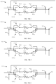
- FIGs. 6A-6E are schematic diagrams illustrating converters 185, respectively, that could be incorporated into the structure 100.
- the current-to-voltage converter 185 of FIG. 6A includes an amplifier 603 and a feedback resistor 604.
- the amplifier 603 has a first input connected to the column interconnect line 151, a second input connected to receive Vvg, and an output.
- the feedback resistor 604 is connected between the output and the first input of the amplifier.
- the feedback resistor 604 can be the same type of programmable resistor as that used in the memory elements. It should be noted that the polarity of the column-specific analog output voltage 189 from the amplifier 603 will be the opposite of that of the column-specific output current on the column interconnect line 151.
- the current-to-voltage converter 185 of FIG. 6B is similarly to the current-to-voltage converter of FIG. 6A but includes additional circuitry to ensure the polarity of the column-specific output current on the column interconnect line and the column-specific output voltage are the same. That is, the current-to-voltage converter 185 includes a first stage and a second stage. The first stage includes first and second n-type field effect transistors (NFETs) 601-602 and the second stage includes the amplifier 603 and the feedback resistor 604. The first NFET 601 is connected in series between the column interconnect line 151 and ground. The second NFET 602 is connected in series between the first input of the amplifier 603 and ground. The drain node of the first NFET 601 can control the gates of the first and second NFETs 601-602.
- NFETs n-type field effect transistors
- the current-to-voltage converter 185 of FIG. 6C includes the amplifier 603, but instead of a feedback resistor, it can include a feedback switched capacitor circuit.
- the amplifier 603 has a first input connected to the column interconnect line 151, a second input connected to receive Vvg, and an output.
- the feedback switched capacitor circuit includes a capacitor 611 that is connected to the output of the amplifier 603 and further connected by a first switch 612 to the first input.
- the feedback switched capacitor circuit can also include a bypass switch 613 that connects the output to the first input of the amplifier 603, bypassing the capacitor 611. In operation, initially the bypass switch 613 is closed to stabilize the high impedance node at Vvg.
- This integration time can be made to be proportional to the temperature coefficient of a programmable resistor used in the memory elements.
- the integration time can be made proportional to a resistor that is made of the same material as the programmable resistors and whose value at the typical temperature of operation is fixed.
- a resistor value can be selected that has a nominal resistor value representative of the variety of resistor values that can appear in the programmable resistors within the array.
- a nominal resistor value e.g., 50k
- this integration time will also determine the magnitude of the output signal and will compensate for the temp-coefficient.
- the value of the output can be held for some duration of time (e.g., track-and-hold circuit), the capacitor 611 can reference some other bias potential, and the power for the op-amp can be turned off to save power.
- the polarity of the column-specific analog output voltage 189 from the amplifier 603 will be the opposite that of the column-specific output current on the column interconnect line 151.
- the current-to-voltage converter 185 of FIG. 6D is similar to the current-to-voltage converter of FIG. 6C but includes additional circuitry to ensure the polarity of the column-specific output current on the column interconnect line and the column-specific output voltage are the same.
- the current-to-voltage converter includes a first stage and a second stage.
- the first stage includes first and second n-type field effect transistors (NFETs) 601-602 and the second stage includes the amplifier 603 and the feedback resistor 604.
- the first NFET 601 is connected in series between the column interconnect line 151 and ground.
- the second NFET 602 is connected in series between the first input of the amplifier 603 and ground.
- the drain node of the first NFET 601 can control the gates of the first and second NFETs 601-602.
- the current-to-voltage converters described above and illustrated in FIGs. 6A-6D are provided for illustration purposes and are not intended to be limiting.
- any other suitable current-to-voltage converter circuit could be incorporated into the structure 100 as a data sensing element.
- the current-to-voltage converter could, alternatively, be in the form of a simple resistor connected between the column interconnect line and ground, as shown in FIG. 6E .
- the structure 200 of FIG. 2 can include data sensing elements 285 and, particularly, subtractors (also referred to herein as subtractor circuits).
- Each subtractor 285 for each column can be connected to the pair of the column interconnect lines 251-252 for that column, can receive the column-specific first output current from the first column interconnect line 251 and the column-specific second output current from the second column interconnect line 252 (e.g., tbI1 C0 and tbI2 C0; ...
- a column-specific analog output parameter 289 e.g., a column-specific analog output voltage (Vout C0-y ) or column-specific analog output current (Iout C0-y )
- Vout C0-y column-specific analog output voltage
- Iout C0-y column-specific analog output current
- Vout C0 or Iout C0 as a function of tbI1 C0 -tbI2 C0; ... ; and Vout Cy or Iout Cy as a function of tbI1 Cy- tbI2 Cy , respectively.
- each first output current is generated on a first bitline 201 in a memory bank as a function of a first programmed resistance state representing a positive weight value and a data input voltage that represents an activation value and since each second output current is generated on the second bitline 202 in each memory bank as a function of a second programmed resistance state representing a negative weight value and the same data input voltage
- the column-specific first output current can represent a solution for a positive side of a dot product computation
- the column-specific second output can represent a solution for a negative side of a dot product computation
- the column-specific analog output parameter e.g., the analog output voltage
- FIGs. 7A-7B are schematic diagrams illustrating subtractors 285, respectively, that could be incorporated into the structure 200.
- the subtractor circuit 285 of FIG. 7A includes a first stage and a second stage.
- the first stage includes first and second n-type field effect transistors (NFETs) 701-702 connected in series between the first and second column interconnect lines 251-252, respectively, of a given column and ground.
- the drain node of the first NFET 701 control the gates of the first and second NFETs 701-702.
- the second stage includes an amplifier 703 and a feedback resistor 704.
- the amplifier has a first input connected to the drain node of the second NFET 702, a second input connected to receive Vvg, and an output.
- the feedback resistor 704 is connected between the output and the first input of the amplifier.
- the feedback resistor 704 can be the same type of programmable resistor used in the memory elements 210.
- the subtractor circuit of FIG. 7B similarly includes a first stage and a second stage.
- the first stage of FIG. 7B is essentially the same as the first stage in FIG. 7A , as discussed above.
- the second stage includes an amplifier 503, but instead of a feedback resistor, it includes a feedback switched capacitor circuit.
- the amplifier 703 has a first input connected to the drain node of the second NFET 702, a second input connected to receive Vvg, and an output.
- the feedback switched capacitor circuit includes a capacitor 711 that is connected to the output of the amplifier 703 and further connected by a first switch 712 to the first input.
- the feedback switched capacitor circuit includes a bypass switch 713 that connects the output to the first input of the amplifier 703, bypassing the capacitor 711.
- the bypass switch 713 is closed to stabilize the high impedance node at Vvg. Then, the bypass switch 713 is opened and there will be a finite integration time across the capacitor 711.
- This integration time can be made proportionate to the value of a programmable resistor used in the memory elements.
- a resistor value can be selected that has a nominal resistor value representative of the variety of resistor values that can appear in the programmable resistors within the array. That is, if the programmable resistors within the array can have values between 20k and 500k, then a nominal resistor value (e.g., 50k) can be selected based on simulations and measurements to minimize the impact of the TCs of the resistors used in the array.
- this integration time will also determine the magnitude of the output signal from the subtractor and will compensate for the temp-coefficient. Furthermore, due to the switched capacitor circuit configuration, the value of the output can be held for some duration of time (e.g., track-and-hold device), the capacitor 711 can reference some other bias potential, and the power for the op-amp can be turned off to save power.
- subtractor circuits described above and illustrated in FIGs. 7A-7B are provided for illustration purposes and are not intended to be limiting. Alternatively, any other suitable subtractor circuit could be incorporated into the structure 200 as a data sensing element.
- FIGs. 1 and 2 are schematic diagrams illustrating embodiments of a structure 100, 200 including a partitioned memory architecture configured for in-memory pipeline processing (e.g., MAC processing).
- MAC processing e.g., MAC processing
- each processing layer e.g., each MAC layer
- a discrete structure configured as described above (i.e., a discrete partitioned memory architecture) with the outputs from one structure for one MAC layer being fed, as inputs, to the next structure for the next MAC layer in the series.
- the number of inputs into a MAC Layer will be greater than the number of outputs from that MAC layer and, thus, the number of inputs to each MAC Layer in the series decreases until a final output is produced.
- THs 170, 270 only serial processing can be performed in order to avoid processing errors. That is, processing of a sample through each structure to the final structure must be completed with the final structure generating a final solution before processing of another sample can begin.
- the presence of the THs 170, 270 in the initial memory banks of each discrete structure 100, 200 in the series enables pipeline processing to be performed.
- the analog voltage outputs from an upstream structure 100, 200 of the series-connected structures are sampled (as data input voltages) and stored (i.e., tracked and held) by THs 170, 270 in the initial memory banks of the adjacent downstream structure 100, 200 in the series, one the THs 170, 270 of the downstream structure are switched to the hold mode, the THs 170, 270 in the upstream structure 100, 200 can switch to the track mode to capture new inputs (i.e., another sample) while downstream processing of the earlier sample is being performed.
- calibration processing refers to a process whereby an actual resistance value of a specific programmable resistor is determined. This actual resistance value can be compared to a desired/expected resistance value to determine whether or not reprogramming of the specific programmable resistor should be performed.
- Veal can be set at some predetermined fixed voltage level that it sufficiently high so that a current output from the specific programmable resistor can be sensed, but sufficiently low to prevent any reprogramming.
- Vcal can range between 0.15V and 0.3V (e.g., 0.2V).
- the control bits 113, 213 for the amplifiers 115, 215 in the structure 100, 200 can be set so that only one specific amplifier 115, 215 in the structure 100, 200 is in an on-state.
- the specific amplifier in the on-state can be in the initial memory bank of one specific row of memory banks at a particular address.
- This specific amplifier 115, 215 can generate and output a level shifted calibration voltage, which is essentially equal to the sum of Vcal plus Vvg. That is, it can add Vvg to Vcal to generate the level shifted calibration voltage.
- This level shifted calibration voltage can be received at the input terminals of the programmable resistors of all memory elements at the same particular address within the same row of memory banks.
- control bits 113, 213 for all other amplifiers 115, 215 in the structure 100, 200 can be set so that the amplifiers output a high impedance (HiZ) state. Additionally, during the calibration mode, each specific bitline connected to each specific programmable resistor to be calibrated can bias be biased to Vvg (e.g., by the feedback buffer circuit 120, 220.1 or 220.2 connected to the specific bitline). All other feedback buffer circuits on all other bitlines are turned off. It should be noted that in the structure 200 of FIG.
- the output current from only one specific programmable resistor is output at the output node of one specific memory bank in the column and received by the data sensing element 185, 285 for that column (via a column interconnect line).
- the data sensing element 185 i.e., the current-to-voltage converter
- the data sensing element 185 can convert that output current to a column-specific analog output voltage 189, which during calibration processing, is indicative of the actual resistance value of the specific programmable resistor.
- the data sensing element 285 i.e., the subtractor
- the data sensing element 285 for the column can compare the output current from the one specific programmable resistor on the column interconnect line to the current on the other column interconnect line of a pair for the column (which is at 0 amps because all output nodes of all memory banks connected to that column interconnect line are also connected to feedback buffer circuits in the off state) and can output a column-specific analog output voltage 289, which during calibration processing is indicative of the actual resistance value of the specific programmable resistor.
- the column-specific analog output voltage 189, 289 can, in turn, be converted to a column-specific digital value 188, 288 by the ADC 187, 287 for the column.
- the column-specific digital value can, for example, be compared to an expected digital value for the specific programmable resistor. If the values differ, a reprogramming processing can be performed (e.g., either immediately or in some subsequent time window designated for reprogramming).
- FIG. 8 is an example of a timing diagram for performing in-memory pipeline processing (e.g., MAC processing including a series of MAC layers) with interspersed calibration processing. As mentioned above, such processing will require multiple instances of the structure 100, 200 described above (one for each MAC layer).
- In-memory pipeline processing begins with the input MAC layer (Layer 1) structure processing a first sample captured and stored by the THs (Sample 1). Time 1, Sample 1 data input voltages are input into the Layer 1 structure (i.e., all activation voltages of Sample 1 are sampled and hold by THs of the Layer 1 structure).
- Time 2 within the Layer 1 structure, the data input voltages of Sample 1 are level-shifted by Vvg and the bitlines are biased to Vvg (i.e., allow settling time for the Vvg buffer).
- Time 3 within the Layer 1 structure, the data sensing elements (i.e., current-to-voltage converters or subtractors, as applicable) are activated.
- Time 4 the column-specific output voltages generated by the data sensing elements of the Layer 1 structure are fed to the THs of the Layer 2 structure.
- Time 5 processing in the Layer 2 structure is again initiated.
- the amplifiers in the Layer 2 structure level-shift the previously received analog voltages from the Layer 1 structure by Vvg and the bitlines are biased to Vvg (i.e., allow settling time for the Vvg buffer).
- Time 6 within the Layer 2 structure, the current-to-voltage converters or subtractors are activated.
- Time 7 the column-specific output voltages generated by the current-to-voltage converters or subtractors of the Layer 2 structure are fed to the THs of a Layer 3 structure, which processes another hidden MAC layer.
- Time 7 within the Layer 3 structure, the column-specific output voltages from the Layer 2 structure are sampled and held by THs as data input voltages.
- Time 8 within the Layer 3 structure, the data input voltages are level-shifted by Vvg and the bitlines are biased to Vvg (i.e., allow settling time for the Vvg buffer).
- Time 9 within the Layer 3 structure, the current-to-voltage converters or subtractors are activated.
- Time 10 the column-specific output voltages generated by the current-to-voltage converters or subtractors of the Layer 3 structure are fed to the THs of a Layer 4 structure.
- Layer structure-to-Layer structure processing continues as described above until the final solution for Sample 1 is output by the final Layer structure in the series.
- Layer 1 can also initiate processing of Sample 2. That is, at Time 4D, the THs of the Layer 1 structure can sample and hold the activation voltages of Sample 2.
- Time 5 within the Layer 1 structure, the data input voltages of Sample 2 are level-shifted by Vvg and the bitlines are biased to Vvg (i.e., allow settling time for the Vvg buffer).
- Time 6 within the Layer 1 structure, the current-to-voltage converters or subtractors, as applicable, are activated.
- Time 7 the column-specific output voltages generated by current-to-voltage converters or subtractors of the Layer 1 structure are fed to the THs of the Layer 2 structure, which processes a hidden MAC layer.
- FIG. 8 only shows MAC processing including three MAC layers with a pause in all MAC processing to perform calibration processing within the Layer 1 structure occurring after processing of Sample 1 in Layer 1 and before processing of Sample 2 in Layer 1.
- FIG. 8 is not intended to be limiting and that such MAC processing typically requires significantly more layers to develop a final solution and pauses for calibration processing can be performed within any Layer because the THs enable storage of inputs.
- FIGs. 9A is a schematic diagram illustrating a structure 900 including the structure 100 of FIG. 1 modified with additional circuitry to enable concurrent in-memory pipeline processing (e.g., MAC processing) and calibration processing.
- FIG. 10A is a schematic diagram illustrating a structure 1000 including the structure 200 of FIG. 2 modified with additional circuitry to enable concurrent in-memory pipeline processing (e.g., MAC processing) and calibration processing.
- the structure 900 of FIG. 9A includes a duplicate pair 910 of single resistor memory elements (e.g., see FIG. 9B and the detailed discussion below) and the structure 1000 of FIG.
- the structure 900 of FIG. 9A and the structure 1000 of FIG. 10A include both operational circuitry for in-memory pipeline processing and calibration circuitry (e.g., calibration supply lines and calibration sense lines for each memory bank and calibration interconnect lines, calibration sensing elements, etc. or each column of memory banks) for calibration processing.
- calibration circuitry e.g., calibration supply lines and calibration sense lines for each memory bank and calibration interconnect lines, calibration sensing elements, etc. or each column of memory banks
- switches connected to opposing end terminals of the programmable resistors of the memory elements of each duplicate pair enable one memory element of the duplicate pair to be connected to the operational circuitry for in-memory pipeline processing and further enable the programmable resistor(s) of the other memory element of the duplicate pair to be individually and selectively connected to the calibration circuitry for on-demand calibration processing or disconnected from both the operational circuitry and the calibration circuitry.
- the structure 900 of FIG. 9A is a modification of the structure 100 of FIG. 1 with additional features labeled in the 900's (e.g., 900, 901, etc.).
- the structure 1000 of FIG. 10A is a modification of the structure 200 of FIG. 2 .
- the structure 900, 1000 can include an array 190, 290 of memory banks 199, 299.
- Each memory bank 199, 299 in structure 900, 1000 can further include operational circuitry and, more particularly, essentially the same circuitry included in the memory banks 199, 299 of the structure 100, 200 discussed above.
- this operational circuitry includes but is not limited to: in each initial memory bank of each row of memory banks, THs 170 and amplifiers 115; optional voltage buffers 116 in one or more downstream memory banks in any row of memory banks 199; and, in each memory bank, a bitline 101 and a feedback buffer circuit 120 connected to both a bias node 133 on the bitline 101 and to an output node 135.
- the structure 900 also includes sets of row interconnect lines 155 that interconnect adjacent memory banks in each row of memory banks, column interconnect lines 151 connected to the output nodes 135 of each memory bank 199 in the same column, and a data sensing element 185 (e.g., a current-to-voltage converter) for each column connected to the column interconnect line 151 for that column.
- a data sensing element 185 e.g., a current-to-voltage converter
- this operational circuitry includes but is not limited to: in each initial memory bank of each row of memory banks, THs 270 and amplifiers 215; optional voltage buffers 216 in one or more downstream memory banks in any row of memory banks 299; and, in each memory bank, a first bitline 201, a second bitline 202, a first feedback buffer circuit 220.1 connected to both a first bias node 233 on the first bitline 201 and a first output node 235, and a second feedback buffer circuit 220.2 connected to both a second bias node 234 on the second bitline 202 and a second output node 236.
- the structure 900 also includes sets of row interconnect lines 155 that interconnect adjacent memory banks in each row of memory banks, column interconnect lines 151 connected to the output nodes 135 of each memory bank 199 in the same column, and a data sensing element 185 (e.g., a current-to-voltage converter) for each column connected to the column interconnect line 151 for that column.
- a data sensing element 185 e.g., a current-to-voltage converter
- the structure 1000 also includes the sets of row interconnect lines 255 that interconnect adjacent memory banks in each row of memory banks, first column interconnect lines 251 connected to the first output nodes 235 of each memory bank 299 in the same column, second column interconnect lines 252 connected to the second output nodes 236 of each memory bank 299 in the same column, and a data sensing element 285 (e.g., a subtractor) for each column connected to the first and second column interconnect lines 251 and 252 for that column.
- a data sensing element 285 e.g., a subtractor
- Each memory bank 199, 299 in the structure 900, 1000 can further include calibration circuitry.
- the calibration circuitry can include a calibration supply line 995, 1095 for supplying a level shifted calibration input voltage to the memory bank 199, 299.
- This level shifted calibration input voltage can be set at a predetermined voltage level that is essentially equal to the sum of a calibration input voltage (Vcal) plus Vvg.
- Vcal can be set at some predetermined fixed voltage level that it sufficiently high so that a current output from the specific programmable resistor can be sensed, but sufficiently low to prevent any reprogramming.
- Vcal can range between 0.15V and 0.3V (e.g., 0.2V).
- the calibration circuitry can further include: a calibration output node 935, 1035; a calibration sense line 901, 1001 including a calibration bias node 933, 1033 at one end; and a calibration feedback buffer circuit 920, 1020 connected to the calibration bias node 933, 1033 and the calibration output node 935, 1035.
- the calibration feedback buffer circuit 920, 1020 can be configured essentially the same as the feedback buffer circuit 120, 220.1-220.2, described above, for biasing the calibration bias node 933, 1033 to Vvg during calibration processing.
- the structure 900, 1000 can also include additional calibration circuitry.
- the additional calibration circuitry can include, for example, calibration interconnect lines 951, 1051 for the columns with each calibration interconnect line for a column connected to the calibration output nodes 935, 1035 of all memory banks 199, 299 in that column, calibration sensing elements 985, 1085 (e.g., current-to-voltage converters) for the columns with each calibration sensing element for a column connected to the calibration interconnect line 951, 1051 for that column, and analog-to-digital converters (ADC) 987, 1087 for the columns with each ADC for a column connected to the calibration sensing element 985,1085 for that column.
- ADC analog-to-digital converters
- FIG. 11 is a schematic diagram illustrating a current-to-voltage converter that can be used in the structure 900 for the calibration sensing elements 985 if/when the data sensing elements 185 are configured in essentially the same manner as the current-to-voltage converter shown in FIG. 6D .
- This same current-to-voltage converter can be used in the structure 1000 for the calibration sensing elements 1085 if/when the data sensing elements 285 are configured in essentially the same manner as the subtractor shown in FIG. 7B .
- the current-to-voltage converter of FIG. 11 includes a first stage and a second stage.
- the first stage includes first and second NFETs 1101-1102 and the second stage includes an amplifier 1103 and a feedback switched capacitor circuit.
- the first NFET 1101 is connected in series between the calibration interconnect line 951, 1051 and GND.
- the second NFET 1102 is connected in series between a first input to the amplifier 1103 and GND.
- the drain node of the first NFET 1101 can control the gates of the first and second NFETs 1101-1102.
- the amplifier 1103 also has a second input connected to receive Vvg and an output.
- the feedback switched capacitor circuit includes a capacitor 1111 that is connected to the output of the amplifier 1103 and further connected by a first switch 1112 to the first input of the amplifier 1103.
- the feedback switched capacitor circuit can also include a bypass switch 1113 that connects the output to the first input of the amplifier 1103, bypassing the capacitor 1111.
- a bypass switch 1113 that connects the output to the first input of the amplifier 1103, bypassing the capacitor 1111.
- the bypass switch 1113 is closed to stabilize the high impedance node at Vvg.
- the bypass switch 1113 is opened and there will be a finite integration time across the capacitor 1111.
- This integration time can be made to be proportionate to the value of a programmable resistor used in the memory elements. For example, a resistor value can be selected that has a nominal resistor value representative of the variety of resistor values that can appear in the programmable resistors within the array.
- a nominal resistor value e.g., 50k
- this integration time will also determine the magnitude of the output signal from the converter and will compensate for the temp-coefficient.
- the value of the output can be held for some duration of time (e.g., track-and-hold circuit), the capacitor 1111 can reference some other bias potential, and the power for the op-amp can be turned off to save power.
- any other suitable current-to-voltage converter circuit could be incorporated into the structure 900, 1000 as a calibration sensing element.
- Each memory bank 199, 299 in the structure 900, 1000 can further include duplicate pairs 910, 1010 of memory elements 110.1-110.2, 210.1-210.2 (as opposed to memory elements 110, 210). That is, in the structure 900, each memory bank 199 can include duplicate pairs 910 of single resistor memory elements 110.1-110.2.
- FIG. 9B is a schematic diagram illustrating a duplicate pair 910. As illustrated in FIGs. 9B-1 to 9B-4 , the single resistor memory element 110.1 and 110.2 can be single programmable resistors 111.1 and 111.2, respectively.
- Each duplicate pair 910 of single resistor memory elements 110.1-110.2 can also include switches at the opposing end terminals of the programmable resistors therein (e.g., see the switches 991.1 at the opposing end terminals of the programmable resistor 111.1 and the switches 991.2 at the opposing end terminals of the programmable resistor 111.2).
- each memory bank 299 can include duplicate pairs 1010 of dual resistor memory elements 210.1-201.2.
- FIG. 10B is a schematic diagram illustrating a duplicate pair 1010 of dual resistor memory elements 210.1-210.2. As illustrated in FIGs.
- each dual resistor memory element 210.1 and 210.2 can be include a first programmable resistor 211.1, 211.2 and a second programmable resistor 212.1, 212.2.
- Each duplicate pair 1010 of dual resistor memory elements 210.1-210.2 can also include switches at the opposing end terminals of each of the programmable resistors therein (e.g., in the dual resistor memory element 210.1, see the switches 1091.1 at the opposing end terminals of the first programmable resistor 211.1 and the switches 1092.1 at the opposing end terminals of the second programmable resistor 212.1; in the dual resistor memory element 210.2, see the switches 1091.2 at the opposing end terminals of the first programmable resistor 211.2 and the switches 1092.2 at the opposing end terminals of the second programmable resistor 212.2).
- switches can include, for example, 3-to-1 multiplexors (3:1 MUXs) at the input terminals of each programmable resistor to allow for selective connection of an operational input node to the input terminal, a calibration supply line to the input terminal, or no operational or calibration circuit component to the input terminal.
- the switches can also include, for example, 1-to-3 multiplexors (1:3 MUXs) at the output terminals of each programmable resistor to allow for selective connection of the output terminal to an operational bitline, to a calibration sense line, or to no operational or calibration circuit component.
- the switches 991.1 at the opposing end terminals of the programmable resistor 111.1 and the switches 991.2 at the opposing end terminals of the programmable resistor 111.2 in the duplicate pair 910 can be controllable so the programmable resistors 111.1 and 111.2 are each connectable to the operational circuitry (e.g., an operational input node and a bitline), connectable to the calibration circuitry (i.e., a calibration supply line and a calibration sense line), and disconnectable from both the operational circuitry and the calibration circuitry.
- the operational circuitry e.g., an operational input node and a bitline
- the calibration circuitry i.e., a calibration supply line and a calibration sense line
- the switches 991.1-991.2 can be controlled so as to selectively connect one programmable resistor of one single resistor memory element of a duplicate pair 910 to the operational circuitry for in-memory pipeline processing and so as to either connect the programmable resistor of the other single resistor memory element of the duplicate pair to the calibration circuitry for calibration processing or disconnect it from both the operational circuitry and the calibration circuitry (e.g., when no calibration processing is being performed or when calibration processing is directed to a different programmable resistor in the same column).
- FIGs. 9B-1 to 9B-4 show various alternative states of the switches 991.1-991.2.
- the switches 1091.1 at the opposing end terminals of the first programmable resistor 211.1, the switches 1092.1 at the opposing end terminals of the second programmable resistor 212.1, the switches 1091.2 at the opposing end terminals of the first programmable resistor 211.2, and the switches 1092.2 at the opposing end terminals of the second programmable resistor 212.2 in the duplicate pair 1010 are controllable so that the programmable resistors 211.1, 211.2, 212.1, 212.2 are each connectable to the operational circuitry (i.e., an operational input node and a first bitline and the operational input node and a second bitline), connectable to the calibration circuitry (i.e., a calibration supply line and a calibration sense line), and disconnectable from both the operational circuitry and the calibration circuitry.
- the operational circuitry i.e., an operational input node and a first bitline and the operational input node and a second bitline
- the calibration circuitry i.e., a calibration supply line and
- the switches 1091.1-1091.2 1092.1-1092.2 can be controlled so as to selectively connect the two programmable resistors of one dual resistor memory element of a duplicate pair 1010 to the operational circuitry for in-memory pipeline processing.
- the switches 1091.1-1091.2 1092.1-1092.2 can further be controlled to connect one programmable resistor of the other dual resistor memory element of the duplicate pair to the calibration circuitry for calibration processing and to disconnect the other from the operational circuitry and the calibration circuit.
- the switches can further be controlled to disconnect both programmable resistors of the other dual resistor memory element of the duplicate pair from both the operational circuitry and the calibration circuitry (e.g., when no calibration processing is being performed or when calibration processing is directed to a different programmable resistor in the same column).
- FIGs. 10B-1 to 10B-6 show various alternative states of the switches 1091.1-1091.2 and 1092.1-1092.2.
- the duplicate pairs 910, 1010 of memory elements and the switches in each of these structures 900, 1000 configured as described above facilitate concurrent performance of both in-memory pipeline processing (e.g., MAC processing) and calibration processing.
- each processing layer e.g., each MAC layer
- each processing layer will typically be handled by a discrete structure configured as described above (i.e., a discrete partitioned memory architecture) with the outputs from one structure for one MAC layer being fed, as inputs, to the next structure for the next MAC layer in the series.
- the number of inputs into a MAC Layer will be greater than the number of outputs from that MAC layer and, thus, the number of inputs to each MAC Layer in the series decreases until a final output is produced.
- the presence of the THs 170, 270 in the initial memory banks enables pipeline processing to be performed.
- the switches in each duplicate pair 910, 1010 of memory elements can be controlled so that one memory element 110.1 or 110.2, 210.1 or 210.2 of each duplicate pair 910, 1010 of memory elements in each memory bank within the array 190, 290 will be connected to the operational circuitry at all times allowing in-memory pipeline processing to proceed essentially as described above with regard to the structure 100 of FIG. 1 or 200 of FIG. 2 .
- the switches in each duplicate pair 910, 1010 of memory elements can further be controlled so that the other memory element of each duplicate pair is disconnected from both the calibration circuitry and the operational circuitry and, thus, idle such that at times only in-memory pipeline processing is performed within the structure.
- calibration processing can be performed concurrently with in-memory pipeline processing.
- calibration processing can also be directed to a single programmable resistor within the structure (i.e., to one specific programmable resistor of one specific memory element of one specific duplicate pair in a specific memory bank of a specific column within the structure) or to a sing programmable transistor within each of one or more columns of the structure (i.e., to one specific programmable resistor of one specific memory element of one specific duplicate pair in one or more columns).
- concurrent calibration processing can be directed to one specific programmable resistor 111.1 or 111.2 of one specific single resistor memory element 110.1 or 110.2 of one specific duplicate pair 910 in a specific memory bank of one specific column, while the other programmable resistor of the other single resistor memory element of the specific duplicate pair is employed for in-memory pipeline processing.
- the switches are controlled to selectively connect the opposing end terminals of the specific programmable resistor to the calibration supply line 995 and the calibration sense line 901 for the specific memory bank.
- the calibration supply line 995 supplies the level shifted calibration input voltage to the input terminal of the specific programmable resistor and the calibration feedback buffer circuit 920 for the specific memory bank biases the calibration bias node 933 on the calibration sense line 901 for the specific memory bank to Vvg. It should be noted that during calibration processing directed to this specific programmable resistor no other programmable resistor in the same specific memory bank or in the same column of memory banks will be connected to calibration circuitry and the calibration feedback buffer circuits 920 in all other memory banks in the same column of memory banks will be in off states. Thus, the only current on the calibration interconnect line 951 is the buffered current from the specific memory bank (which was generated due to the application of the level shifted calibration voltage to the input terminal of the specific programmable resistor).
- concurrent calibration processing can be directed to one specific programmable resistor of the two programmable resistors of one specific dual resistor memory element 210.1 or 210.2 of one specific duplicate pair 1010 in a specific memory bank of one specific column of memory banks, while the other programmable resistor of the specific dual resistor element of the specific duplicate pair is disconnected from both the operational circuitry and the calibration circuit and while the other dual resistor memory element of the specific duplicate pair is employed for in-memory pipeline processing.
- the switches are controlled to selectively connect the opposing end terminals of the specific programmable resistor to the calibration supply line 1095 and the calibration sense line 1001 for the specific memory bank and to disconnect the other programmable resistor of the specific dual resistor memory element from both the operational circuitry and the calibration circuitry.
- the calibration supply line 1095 supplies the level shifted calibration input voltage to the input terminal of the specific programmable resistor and the calibration feedback buffer circuit 1020 for the specific memory bank biases the calibration bias node 1033 on the calibration sense line 1001 for the specific memory bank to Vvg.
- the current on the calibration interconnect line 951, 1051 for the specific column i.e., the column-specific calibration output current
- the calibration sensing element 985, 1085 e.g., a current-to-voltage converter, as discussed above and illustrated in FIG. 11 .
- the calibration sensing element 985, 1085 can convert the column-specific calibration output current to a column-specific calibration output voltage 989, 1089.
- the column-specific calibration output voltage 989, 1089 can, in turn, be converted to a column-specific digital value 988, 1088 by the ADC 987, 1087 for the specific column.
- the column-specific digital value 988, 1088 can, for example, be compared to an expected digital value for the specific programmable resistor. If the values differ, a reprogramming processing can be performed (e.g., either immediately or in some subsequent time window designated for reprogramming).
- FIG. 12 is an example of a timing diagram for concurrently performing in-memory pipeline processing and calibration processing using the structure 900 or 1000.
- the structures disclosed herein can include additional control and connecting circuitry to both feed outputs from structure to the next and to concurrently perform calibration processing (including controlling operation of the switches that selectively connect or disconnect specific memory elements to the operational circuitry, the calibration circuitry, or neither).
- control and connecting circuitry are known in the art and, thus, the details thereof have been omitted from this specification in order to allow the reader to focus on the salient aspects of the disclosed embodiments.
- the structures disclosed herein can also include additional circuitry (not shown) to implement other operational modes (e.g., program modes).
- additional circuitry not shown to implement other operational modes (e.g., program modes).
- the programmable resistors of the memory elements are programmed to particular resistance states and can further be reprogrammed, if necessary, following calibration processing.
- the memory elements are described and shown in the figures as being either single resistor memory elements or dual resistor memory elements. However, it should be understood that the figures and description thereof are not intended to be limiting. Alternatively, the disclosed structures could include memory elements with more than two programmable resistors. In this case, each memory bank would have a corresponding number of bitlines with feedback buffer circuits and each column of memory banks would have additional circuitry (e.g., addition or subtraction circuitry) to combine the current outputs from all bitlines as appropriate depending upon whether the resistances states of the programmable resistors represent positive or negative weight values.
- additional circuitry e.g., addition or subtraction circuitry
- laterally is used herein to describe the relative locations of elements and, more particularly, to indicate that an element is positioned to the side of another element as opposed to above or below the other element, as those elements are oriented and illustrated in the drawings.
- an element that is positioned laterally adjacent to another element will be beside the other element
- an element that is positioned laterally immediately adjacent to another element will be directly beside the other element
- an element that laterally surrounds another element will be adjacent to and border the outer sidewalls of the other element.
Landscapes
- Engineering & Computer Science (AREA)
- Computer Hardware Design (AREA)
- Theoretical Computer Science (AREA)
- Health & Medical Sciences (AREA)
- Life Sciences & Earth Sciences (AREA)
- Biomedical Technology (AREA)
- Physics & Mathematics (AREA)
- Neurology (AREA)
- General Engineering & Computer Science (AREA)
- General Health & Medical Sciences (AREA)
- Molecular Biology (AREA)
- Computing Systems (AREA)
- Biophysics (AREA)
- General Physics & Mathematics (AREA)
- Mathematical Physics (AREA)
- Evolutionary Computation (AREA)
- Computational Linguistics (AREA)
- Software Systems (AREA)
- Artificial Intelligence (AREA)
- Data Mining & Analysis (AREA)
- Microelectronics & Electronic Packaging (AREA)
- Semiconductor Memories (AREA)
- Indication And Recording Devices For Special Purposes And Tariff Metering Devices (AREA)
- Measuring Volume Flow (AREA)
- Techniques For Improving Reliability Of Storages (AREA)
- Semiconductor Integrated Circuits (AREA)
Applications Claiming Priority (1)
| Application Number | Priority Date | Filing Date | Title |
|---|---|---|---|
| US18/045,529 US12136468B2 (en) | 2022-10-11 | 2022-10-11 | Calibration methods and structures for partitioned memory architecture with single resistor or dual resistor memory elements |
Publications (2)
| Publication Number | Publication Date |
|---|---|
| EP4354443A2 true EP4354443A2 (de) | 2024-04-17 |
| EP4354443A3 EP4354443A3 (de) | 2024-08-21 |
Family
ID=87517283
Family Applications (1)
| Application Number | Title | Priority Date | Filing Date |
|---|---|---|---|
| EP23187997.4A Pending EP4354443A3 (de) | 2022-10-11 | 2023-07-27 | Kalibrierungsverfahren und -strukturen für partitionierte speicherarchitektur mit einzelwiderstand oder doppelwiderstandspeicherelementen |
Country Status (3)
| Country | Link |
|---|---|
| US (1) | US12136468B2 (de) |
| EP (1) | EP4354443A3 (de) |
| CN (1) | CN117877558A (de) |
Families Citing this family (1)
| Publication number | Priority date | Publication date | Assignee | Title |
|---|---|---|---|---|
| CN116486857B (zh) * | 2023-05-17 | 2024-04-02 | 北京大学 | 一种基于电荷再分配的存内计算电路 |
Family Cites Families (27)
| Publication number | Priority date | Publication date | Assignee | Title |
|---|---|---|---|---|
| US4906865A (en) | 1988-12-09 | 1990-03-06 | Intel Corporation | Sample and hold circuit for temporal associations in a neural network |
| DE102004056911B4 (de) | 2004-11-25 | 2010-06-02 | Qimonda Ag | Speicherschaltung sowie Verfahren zum Auslesen eines Speicherdatums aus einer solchen Speicherschaltung |
| KR101367659B1 (ko) | 2007-07-12 | 2014-02-25 | 삼성전자주식회사 | 읽기 에러를 줄일 수 있는 멀티 레벨 상 변화 메모리 장치및 그것의 읽기 방법 |
| KR20140023806A (ko) | 2012-08-17 | 2014-02-27 | 삼성전자주식회사 | 자기 저항 메모리 장치의 배치 구조 |
| KR102154296B1 (ko) | 2012-12-18 | 2020-09-14 | 삼성전자 주식회사 | 저항체를 이용한 비휘발성 메모리 장치의 구동 방법 및 비휘발성 메모리 장치 |
| KR102212750B1 (ko) | 2014-07-23 | 2021-02-05 | 삼성전자주식회사 | 저항성 메모리 장치, 이를 포함하는 메모리 시스템 및 저항성 메모리 장치의 데이터 독출 방법 |
| KR20160141890A (ko) | 2015-06-01 | 2016-12-12 | 에스케이하이닉스 주식회사 | 전자 장치 |
| US9666273B2 (en) | 2015-06-18 | 2017-05-30 | International Business Machines Corporation | Determining a cell state of a resistive memory cell |
| GB2552014B (en) | 2016-07-07 | 2020-05-13 | Advanced Risc Mach Ltd | Reconfigurable artificial neural networks comprising programmable non-volatile memory elements |
| JP6481667B2 (ja) * | 2016-07-20 | 2019-03-13 | 株式会社デンソー | ニューラルネットワーク回路 |
| US9997242B2 (en) | 2016-10-14 | 2018-06-12 | Arm Ltd. | Method, system and device for non-volatile memory device state detection |
| US10922608B2 (en) | 2017-03-08 | 2021-02-16 | Arm Ltd | Spiking neural network |
| JP2018156701A (ja) | 2017-03-16 | 2018-10-04 | 東芝メモリ株式会社 | 不揮発性半導体記憶装置 |
| US10726914B2 (en) | 2017-04-14 | 2020-07-28 | Attopsemi Technology Co. Ltd | Programmable resistive memories with low power read operation and novel sensing scheme |
| US9934838B1 (en) | 2017-05-10 | 2018-04-03 | International Business Machines Corporation | Pulse shaping unit cell and array for symmetric updating |
| US10290679B1 (en) | 2018-03-09 | 2019-05-14 | Globalfoundries Singapore Pte. Ltd. | High-Density STT-MRAM with 3D arrays of MTJs in multiple levels of interconnects and method for producing the same |
| US10891080B1 (en) | 2018-06-04 | 2021-01-12 | Mentium Technologies Inc. | Management of non-volatile memory arrays |
| GB2583790A (en) | 2019-05-07 | 2020-11-11 | Cirrus Logic Int Semiconductor Ltd | Computing circuitry |
| US20200378513A1 (en) | 2019-05-31 | 2020-12-03 | Robert Kowalski | Heated Faucet Cover |
| US20210064379A1 (en) | 2019-08-29 | 2021-03-04 | Arm Limited | Refactoring MAC Computations for Reduced Programming Steps |
| US11393512B2 (en) | 2019-11-15 | 2022-07-19 | Taiwan Semiconductor Manufacturing Company, Ltd. | Memory device |
| CN113139641A (zh) | 2020-01-20 | 2021-07-20 | 华为技术有限公司 | 神经网络系统及神经网络计算方法 |
| US11335401B1 (en) * | 2021-01-28 | 2022-05-17 | National Tsing Hua University | Memory unit with multiple word lines for nonvolatile computing-in-memory applications and current calibrating method thereof |
| US11837281B2 (en) | 2021-08-31 | 2023-12-05 | Integrated Circuit, Interface Circuit And Method | Integrated circuit, interface circuit and method |
| US11901004B2 (en) | 2022-04-08 | 2024-02-13 | Taiwan Semiconductor Manufacturing Company, Ltd. | Memory array, memory structure and operation method of memory array |
| US11894052B2 (en) | 2022-04-12 | 2024-02-06 | Stmicroelectronics S.R.L. | Compensated analog computation for an in-memory computation system |
| US12354656B2 (en) | 2022-08-01 | 2025-07-08 | Synopsys, Inc. | Reducing memory device bitline leakage |
-
2022
- 2022-10-11 US US18/045,529 patent/US12136468B2/en active Active
-
2023
- 2023-07-27 EP EP23187997.4A patent/EP4354443A3/de active Pending
- 2023-10-10 CN CN202311306531.9A patent/CN117877558A/zh active Pending
Also Published As
| Publication number | Publication date |
|---|---|
| CN117877558A (zh) | 2024-04-12 |
| EP4354443A3 (de) | 2024-08-21 |
| US12136468B2 (en) | 2024-11-05 |
| US20240119974A1 (en) | 2024-04-11 |
Similar Documents
| Publication | Publication Date | Title |
|---|---|---|
| EP3370145B1 (de) | Analoge multiplizierer-akkumulatoren | |
| US12242949B2 (en) | Compute-in-memory devices, systems and methods of operation thereof | |
| EP1612801B1 (de) | Stromsparendes Lesen in magnetischen Speicheranordnungen | |
| US8203893B2 (en) | Write current compensation using word line boosting circuitry | |
| US7570507B2 (en) | Quasi-differential read operation | |
| US11195580B2 (en) | Integrated pixel and two-terminal non-volatile memory cell and an array of cells for deep in-sensor, in-memory computing | |
| US12198039B2 (en) | Synapse memory | |
| KR20180013789A (ko) | 터너리 내용 주소화 메모리 | |
| US20200202202A1 (en) | Synapse circuit with memory | |
| CN115862708A (zh) | 忆阻器阵列的操作方法、数据处理装置 | |
| EP4354443A2 (de) | Kalibrierungsverfahren und -strukturen für partitionierte speicherarchitektur mit einzelwiderstand oder doppelwiderstandspeicherelementen | |
| EP4354436A1 (de) | Partitionierte speicherarchitektur und verfahren zur wiederholten verwendung der architektur für mehrere speicherinterne verarbeitungsschichten | |
| EP4354438A1 (de) | Partitionierte speicherarchitektur mit einzelwiderstand oder doppelwiderstandsspeicherelementen zur in-memory-pipeline-verarbeitung | |
| EP4354439A1 (de) | Partitionierte speicherarchitektur mit speicherelementen mit zwei widerständen zur seriellen verarbeitung im speicher | |
| US11645503B2 (en) | Multibit neural network | |
| US9761309B2 (en) | Sensing circuit for resistive memory array | |
| US12211585B2 (en) | Partitioned memory architecture with single resistor memory elements for in-memory serial processing | |
| TWI845270B (zh) | 記憶體內計算記憶體裝置及記憶體內計算方法 | |
| US12406723B2 (en) | Voltage-mode crossbar circuits | |
| CN117437961A (zh) | 用于存储器内运算的存储器装置 |
Legal Events
| Date | Code | Title | Description |
|---|---|---|---|
| PUAI | Public reference made under article 153(3) epc to a published international application that has entered the european phase |
Free format text: ORIGINAL CODE: 0009012 |
|
| STAA | Information on the status of an ep patent application or granted ep patent |
Free format text: STATUS: REQUEST FOR EXAMINATION WAS MADE |
|
| 17P | Request for examination filed |
Effective date: 20230727 |
|
| AK | Designated contracting states |
Kind code of ref document: A2 Designated state(s): AL AT BE BG CH CY CZ DE DK EE ES FI FR GB GR HR HU IE IS IT LI LT LU LV MC ME MK MT NL NO PL PT RO RS SE SI SK SM TR |
|
| PUAL | Search report despatched |
Free format text: ORIGINAL CODE: 0009013 |
|
| AK | Designated contracting states |
Kind code of ref document: A3 Designated state(s): AL AT BE BG CH CY CZ DE DK EE ES FI FR GB GR HR HU IE IS IT LI LT LU LV MC ME MK MT NL NO PL PT RO RS SE SI SK SM TR |
|
| RIC1 | Information provided on ipc code assigned before grant |
Ipc: G11C 11/16 20060101ALI20240718BHEP Ipc: G11C 11/54 20060101ALI20240718BHEP Ipc: G11C 7/12 20060101ALI20240718BHEP Ipc: G11C 7/10 20060101ALI20240718BHEP Ipc: G11C 29/02 20060101AFI20240718BHEP |