EP4350767A1 - Semiconductor structure and method for manufacturing same - Google Patents
Semiconductor structure and method for manufacturing same Download PDFInfo
- Publication number
- EP4350767A1 EP4350767A1 EP22924568.3A EP22924568A EP4350767A1 EP 4350767 A1 EP4350767 A1 EP 4350767A1 EP 22924568 A EP22924568 A EP 22924568A EP 4350767 A1 EP4350767 A1 EP 4350767A1
- Authority
- EP
- European Patent Office
- Prior art keywords
- power supply
- substrate
- semiconductor structure
- wiring layer
- frame
- Prior art date
- Legal status (The legal status is an assumption and is not a legal conclusion. Google has not performed a legal analysis and makes no representation as to the accuracy of the status listed.)
- Granted
Links
Images




Classifications
-
- H—ELECTRICITY
- H10—SEMICONDUCTOR DEVICES; ELECTRIC SOLID-STATE DEVICES NOT OTHERWISE PROVIDED FOR
- H10W—GENERIC PACKAGES, INTERCONNECTIONS, CONNECTORS OR OTHER CONSTRUCTIONAL DETAILS OF DEVICES COVERED BY CLASS H10
- H10W90/00—Package configurations
- H10W90/701—Package configurations characterised by the relative positions of pads or connectors relative to package parts
-
- H—ELECTRICITY
- H10—SEMICONDUCTOR DEVICES; ELECTRIC SOLID-STATE DEVICES NOT OTHERWISE PROVIDED FOR
- H10W—GENERIC PACKAGES, INTERCONNECTIONS, CONNECTORS OR OTHER CONSTRUCTIONAL DETAILS OF DEVICES COVERED BY CLASS H10
- H10W20/00—Interconnections in chips, wafers or substrates
- H10W20/20—Interconnections within wafers or substrates, e.g. through-silicon vias [TSV]
-
- H—ELECTRICITY
- H10—SEMICONDUCTOR DEVICES; ELECTRIC SOLID-STATE DEVICES NOT OTHERWISE PROVIDED FOR
- H10W—GENERIC PACKAGES, INTERCONNECTIONS, CONNECTORS OR OTHER CONSTRUCTIONAL DETAILS OF DEVICES COVERED BY CLASS H10
- H10W20/00—Interconnections in chips, wafers or substrates
- H10W20/40—Interconnections external to wafers or substrates, e.g. back-end-of-line [BEOL] metallisations or vias connecting to gate electrodes
- H10W20/482—Interconnections external to wafers or substrates, e.g. back-end-of-line [BEOL] metallisations or vias connecting to gate electrodes for individual devices provided for in groups H10D8/00 - H10D48/00, e.g. for power transistors
- H10W20/484—Interconnections having extended contours, e.g. pads having mesh shape or interconnections comprising connected parallel stripes
-
- H—ELECTRICITY
- H10—SEMICONDUCTOR DEVICES; ELECTRIC SOLID-STATE DEVICES NOT OTHERWISE PROVIDED FOR
- H10W—GENERIC PACKAGES, INTERCONNECTIONS, CONNECTORS OR OTHER CONSTRUCTIONAL DETAILS OF DEVICES COVERED BY CLASS H10
- H10W70/00—Package substrates; Interposers; Redistribution layers [RDL]
- H10W70/40—Leadframes
-
- H—ELECTRICITY
- H10—SEMICONDUCTOR DEVICES; ELECTRIC SOLID-STATE DEVICES NOT OTHERWISE PROVIDED FOR
- H10W—GENERIC PACKAGES, INTERCONNECTIONS, CONNECTORS OR OTHER CONSTRUCTIONAL DETAILS OF DEVICES COVERED BY CLASS H10
- H10W72/00—Interconnections or connectors in packages
- H10W72/071—Connecting or disconnecting
-
- H—ELECTRICITY
- H10—SEMICONDUCTOR DEVICES; ELECTRIC SOLID-STATE DEVICES NOT OTHERWISE PROVIDED FOR
- H10W—GENERIC PACKAGES, INTERCONNECTIONS, CONNECTORS OR OTHER CONSTRUCTIONAL DETAILS OF DEVICES COVERED BY CLASS H10
- H10W90/00—Package configurations
-
- H—ELECTRICITY
- H10—SEMICONDUCTOR DEVICES; ELECTRIC SOLID-STATE DEVICES NOT OTHERWISE PROVIDED FOR
- H10W—GENERIC PACKAGES, INTERCONNECTIONS, CONNECTORS OR OTHER CONSTRUCTIONAL DETAILS OF DEVICES COVERED BY CLASS H10
- H10W90/00—Package configurations
- H10W90/811—Multiple chips on leadframes
-
- H—ELECTRICITY
- H10—SEMICONDUCTOR DEVICES; ELECTRIC SOLID-STATE DEVICES NOT OTHERWISE PROVIDED FOR
- H10W—GENERIC PACKAGES, INTERCONNECTIONS, CONNECTORS OR OTHER CONSTRUCTIONAL DETAILS OF DEVICES COVERED BY CLASS H10
- H10W95/00—Packaging processes not covered by the other groups of this subclass
-
- H—ELECTRICITY
- H10—SEMICONDUCTOR DEVICES; ELECTRIC SOLID-STATE DEVICES NOT OTHERWISE PROVIDED FOR
- H10W—GENERIC PACKAGES, INTERCONNECTIONS, CONNECTORS OR OTHER CONSTRUCTIONAL DETAILS OF DEVICES COVERED BY CLASS H10
- H10W20/00—Interconnections in chips, wafers or substrates
- H10W20/40—Interconnections external to wafers or substrates, e.g. back-end-of-line [BEOL] metallisations or vias connecting to gate electrodes
- H10W20/41—Interconnections external to wafers or substrates, e.g. back-end-of-line [BEOL] metallisations or vias connecting to gate electrodes characterised by their conductive parts
- H10W20/427—Power or ground buses
-
- H—ELECTRICITY
- H10—SEMICONDUCTOR DEVICES; ELECTRIC SOLID-STATE DEVICES NOT OTHERWISE PROVIDED FOR
- H10W—GENERIC PACKAGES, INTERCONNECTIONS, CONNECTORS OR OTHER CONSTRUCTIONAL DETAILS OF DEVICES COVERED BY CLASS H10
- H10W72/00—Interconnections or connectors in packages
- H10W72/01—Manufacture or treatment
-
- H—ELECTRICITY
- H10—SEMICONDUCTOR DEVICES; ELECTRIC SOLID-STATE DEVICES NOT OTHERWISE PROVIDED FOR
- H10W—GENERIC PACKAGES, INTERCONNECTIONS, CONNECTORS OR OTHER CONSTRUCTIONAL DETAILS OF DEVICES COVERED BY CLASS H10
- H10W72/00—Interconnections or connectors in packages
- H10W72/20—Bump connectors, e.g. solder bumps or copper pillars; Dummy bumps; Thermal bumps
- H10W72/231—Shapes
- H10W72/234—Cross-sectional shape, i.e. in side view
-
- H—ELECTRICITY
- H10—SEMICONDUCTOR DEVICES; ELECTRIC SOLID-STATE DEVICES NOT OTHERWISE PROVIDED FOR
- H10W—GENERIC PACKAGES, INTERCONNECTIONS, CONNECTORS OR OTHER CONSTRUCTIONAL DETAILS OF DEVICES COVERED BY CLASS H10
- H10W72/00—Interconnections or connectors in packages
- H10W72/20—Bump connectors, e.g. solder bumps or copper pillars; Dummy bumps; Thermal bumps
- H10W72/241—Dispositions, e.g. layouts
- H10W72/244—Dispositions, e.g. layouts relative to underlying supporting features, e.g. bond pads, RDLs or vias
-
- H—ELECTRICITY
- H10—SEMICONDUCTOR DEVICES; ELECTRIC SOLID-STATE DEVICES NOT OTHERWISE PROVIDED FOR
- H10W—GENERIC PACKAGES, INTERCONNECTIONS, CONNECTORS OR OTHER CONSTRUCTIONAL DETAILS OF DEVICES COVERED BY CLASS H10
- H10W72/00—Interconnections or connectors in packages
- H10W72/834—Interconnections on sidewalls of chips
-
- H—ELECTRICITY
- H10—SEMICONDUCTOR DEVICES; ELECTRIC SOLID-STATE DEVICES NOT OTHERWISE PROVIDED FOR
- H10W—GENERIC PACKAGES, INTERCONNECTIONS, CONNECTORS OR OTHER CONSTRUCTIONAL DETAILS OF DEVICES COVERED BY CLASS H10
- H10W72/00—Interconnections or connectors in packages
- H10W72/90—Bond pads, in general
- H10W72/941—Dispositions of bond pads
- H10W72/944—Dispositions of multiple bond pads
-
- H—ELECTRICITY
- H10—SEMICONDUCTOR DEVICES; ELECTRIC SOLID-STATE DEVICES NOT OTHERWISE PROVIDED FOR
- H10W—GENERIC PACKAGES, INTERCONNECTIONS, CONNECTORS OR OTHER CONSTRUCTIONAL DETAILS OF DEVICES COVERED BY CLASS H10
- H10W90/00—Package configurations
- H10W90/20—Configurations of stacked chips
- H10W90/291—Configurations of stacked chips characterised by containers, encapsulations, or other housings for the stacked chips
-
- H—ELECTRICITY
- H10—SEMICONDUCTOR DEVICES; ELECTRIC SOLID-STATE DEVICES NOT OTHERWISE PROVIDED FOR
- H10W—GENERIC PACKAGES, INTERCONNECTIONS, CONNECTORS OR OTHER CONSTRUCTIONAL DETAILS OF DEVICES COVERED BY CLASS H10
- H10W90/00—Package configurations
- H10W90/20—Configurations of stacked chips
- H10W90/293—Configurations of stacked chips characterised by non-galvanic coupling between the chips, e.g. capacitive coupling
-
- H—ELECTRICITY
- H10—SEMICONDUCTOR DEVICES; ELECTRIC SOLID-STATE DEVICES NOT OTHERWISE PROVIDED FOR
- H10W—GENERIC PACKAGES, INTERCONNECTIONS, CONNECTORS OR OTHER CONSTRUCTIONAL DETAILS OF DEVICES COVERED BY CLASS H10
- H10W90/00—Package configurations
- H10W90/20—Configurations of stacked chips
- H10W90/297—Configurations of stacked chips characterised by the through-semiconductor vias [TSVs] in the stacked chips
-
- H—ELECTRICITY
- H10—SEMICONDUCTOR DEVICES; ELECTRIC SOLID-STATE DEVICES NOT OTHERWISE PROVIDED FOR
- H10W—GENERIC PACKAGES, INTERCONNECTIONS, CONNECTORS OR OTHER CONSTRUCTIONAL DETAILS OF DEVICES COVERED BY CLASS H10
- H10W90/00—Package configurations
- H10W90/701—Package configurations characterised by the relative positions of pads or connectors relative to package parts
- H10W90/721—Package configurations characterised by the relative positions of pads or connectors relative to package parts of bump connectors
- H10W90/722—Package configurations characterised by the relative positions of pads or connectors relative to package parts of bump connectors between stacked chips
-
- H—ELECTRICITY
- H10—SEMICONDUCTOR DEVICES; ELECTRIC SOLID-STATE DEVICES NOT OTHERWISE PROVIDED FOR
- H10W—GENERIC PACKAGES, INTERCONNECTIONS, CONNECTORS OR OTHER CONSTRUCTIONAL DETAILS OF DEVICES COVERED BY CLASS H10
- H10W90/00—Package configurations
- H10W90/701—Package configurations characterised by the relative positions of pads or connectors relative to package parts
- H10W90/721—Package configurations characterised by the relative positions of pads or connectors relative to package parts of bump connectors
- H10W90/726—Package configurations characterised by the relative positions of pads or connectors relative to package parts of bump connectors between a chip and a stacked lead frame, conducting package substrate or heat sink
Definitions
- the present application relates to the field of semiconductors, and more particularly, to a semiconductor structure and a method for fabricating the same.
- HBM high bandwidth memory
- a memory chip stacking technology represented by the HBM an original one-dimensional memory layout is extended to a three-dimensional one. That is, a plurality of memory chips are stacked together and packaged, thereby greatly improving density of the memory chips, and achieving a large capacity and high bandwidth.
- Embodiments of the present application provide a semiconductor structure and a method for fabricating the same, which is at least beneficial to improve the performance of the semiconductor structure.
- an aspect of the embodiments of the present application provides a semiconductor structure, which includes: a substrate having a power supply port; a memory module positioned on an upper surface of the substrate; and a lead frame.
- the memory module includes a plurality of memory chips stacked in a first direction, where the first direction is parallel to the upper surface of the substrate.
- Each of the memory chips has a power supply signal line, at least one of the memory chips has a power supply wiring layer, and the power supply signal line is electrically connected to the power supply wiring layer.
- the power supply wiring layer is positioned in the memory module, and an end surface of the power supply wiring layer far away from the substrate is exposed by the memory module.
- a solder bump is further provided on the end surface, and the lead frame is connected to the solder bump and is also electrically connected to the power supply port.
- another aspect of the embodiments of the present application also provides a method for fabricating a semiconductor structure.
- the method includes: providing a substrate having a power supply port; providing a memory module, where the memory module includes a plurality of memory chips stacked in a first direction, each of the plurality of memory chips has a power supply signal line, at least one of the plurality of memory chips has a power supply wiring layer, the power supply signal line is electrically connected to the power supply wiring layer, the power supply wiring layer is positioned in the memory module, an end surface of the power supply wiring layer far away from the substrate is exposed by the memory module, a solder bump is further provided on the end surface; fixing the memory module to the substrate, where the first direction is parallel to the upper surface of the substrate; providing a lead frame; and connecting the lead frame to the solder bump, and electrically connecting the lead frame to the power supply port.
- a plurality of memory chips are stacked in a direction parallel to the substrate. Therefore, the plurality of memory chips have an equal communication distance, which is advantageous to unifying communication delay and increasing operating speed.
- the power supply wiring layer in the memory chip can lead the power supply signal lines out of the memory chip, so as to achieve wired power supply. The stability and reliability of wired power supply is relatively high.
- the solder bump is connected to the lead frame, so as to improve the strength of the structure.
- a high bandwidth memory, HBM adopts a parallel stacking mode where front surfaces of a plurality of memory chips 200 are parallel to an upper surface of a substrate 300. That is, an arrangement direction of the plurality of memory chips 200 is perpendicular to the upper surface of the substrate 300.
- a communication distance between the memory chip 200 at the uppermost layer and a logic chip 400 has larger difference from a communication distance between the memory chip 200 at the lowermost layer and the logic chip 400, resulting in larger difference between communication delay of different memory chips 200 and communication delay the logic chip 400, which has a negative effect on an operating speed of a product.
- a power supply mode of a semiconductor structure may also have an effect on its performance.
- Embodiments of the present application provide a semiconductor structure, where a plurality of memory chips are stacked in a direction parallel to an upper surface of a substrate. That is, an arrangement direction of the plurality of memory chips is parallel to the upper surface of the substrate. Therefore, the plurality of memory chips have an equal communication distance, which is advantageous to unifying communication delay and increasing operating speed.
- a power supply wiring layer can change a layout of power supply signal lines and lead the power supply signal lines out of a memory module. That is, reliability of power supply can be improved by means of wired power supply.
- a solder bump causes connection between a lead frame and a memory module to be firmer, and the lead frame can specify layout of a power supply path, thereby ensuring stability of power supply.
- an embodiment of the present application provides a semiconductor structure, which includes: a substrate 9 having a power supply port 92; a memory module 100 positioned on an upper surface of the substrate 9; and a lead frame 7.
- the memory module 100 includes a plurality of memory chips 1 stacked in a first direction X, where the first direction X is parallel to the upper surface of the substrate 9.
- Each of the memory chips 1 has a power supply signal line 12, at least one of the memory chips 1 has a power supply wiring layer 2, and the power supply signal line 12 is electrically connected to the power supply wiring layer 2.
- the power supply wiring layer 2 is positioned in the memory module 100, and an end surface 14 of the power supply wiring layer 2 far away from the substrate 9 is exposed by the memory module 100.
- a solder bump 8 is further provided on the end surface 14, and the lead frame 7 is connected to the solder bump 8 and is also electrically connected to the power supply port 92.
- Such design at least includes following effects.
- the power supply wiring layer 2 may lead out the power supply signal line 12, to provide wired power supply to the memory chip 1, thereby improving the stability of power supply.
- the surface of the memory chip 1 includes a front surface and a back surface opposite to each other, and a side surface connected between the front surface and the back surface, where an area of the front surface and an area of the back surface are larger than that of the side surface.
- a plane where the power supply wiring layer 21 is positioned is perpendicular to the upper surface of the substrate 9. That is, the power supply wiring layer 21 may be positioned on the front surface or the back surface of the memory chip 1 to connect the power supply signal line 12.
- the solder bump 1 not only can electrically connect the power supply wiring layer 2 to the lead frame 7, but also can fix the lead frame 7, thereby improving structural strength.
- the lead frame 7 is not easily deformed due to higher strength, such that a direction of a wired power supply path can be specified.
- the plurality of memory chips 1 are stacked along the first direction X. That is, the arrangement direction of the plurality of memory chips 1 is parallel to the substrate 9. In this way, the side surface of the memory chip 1 faces toward the substrate 9. Because the area of the side surface of the memory chip 1 is smaller, an occupied area of the upper surface of the substrate 9 is smaller, which is advantageous to increasing number of the memory chips 1 stacked.
- the semiconductor structure has the first direction X, a second direction Y, and a third direction Z.
- the first direction X is the stacking direction of the memory chips 1
- the second direction Y is perpendicular to the first direction X and is parallel to the upper surface of the substrate 9
- the third direction Z is perpendicular to the upper surface of the substrate 9.
- the plurality of memory chips 1 may be stacked in a hybrid bonding manner.
- a dielectric layer 43 is further provided on the surface of each of the memory chips 1, and the dielectric layers 43 of the adjacent memory chips 1 may be connected together by an acting force such as a molecular force.
- a bonding portion 42 may also be provided on the surface of each of the memory chips 1, and the adjacent bonding portions 42 are bonded and connected together under a heating condition. That is, the dielectric layer 43 is made of an insulating material and can play an isolation role; and the bonding portion 42 is made of a conductive material and can play an electrical connection role.
- the dielectric layer 43 also exposes an end surface 4 of the power supply wiring layer 2 facing away from the substrate 9 and covers the surface of the power supply wiring layer 2 except the end surface 4.
- the memory chip 1 may be a chip such as a dynamic random access memory, DRAM or a static random-access memory, SRAM.
- the adjacent memory chips 1 may all be stacked in the manner that the front surface faces the back surface, which is advantageous to unifying the step of bonding the memory chips 1, such that the production process is simpler.
- the adjacent memory chips 1 may also be stacked in a manner where the front surface faces the front surface or the back surface faces the back surface.
- the front surface of the memory chip 1 may also be understood as an active surface 13, and the back surface of the memory chip 1 may be understood as an inactive surface opposite to the active surface 13.
- the power supply wiring layer 2 and the power supply signal line 12 will be described in detail below.
- the power supply wiring layer 2 may be positioned on the front surface of the memory chip 1. That is, the power supply wiring layer 2 extends along the active surface 13 of the memory chip 1. Therefore, the power supply wiring layer 2 may be fabricated by means of the original back-end process after the fabrication of the components in the memory chip 1 is completed, such that the process is simpler. In addition, the power supply wiring layer 2 may extend only at the edge position close to a side of the active surface 13 of the memory chip 1 without covering the active surface 13 of the entire memory chip 1, so the contact area between the power supply wiring layer 2 and the memory chip 1 is small, which reduces the influence of heat generation of the power supply wiring layer 2 on the memory chip 1.
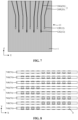
- each memory chip 1 has the plurality of power supply signal lines 12, and the power supply signal line 12 extends from the inside of the memory chip 1 to the active surface 13 to be connected to the power supply wiring layer 2.
- Different power supply signal lines 12 may provide different voltage signals such as digital signals or analog signals for the components in the memory chip 1.
- the power supply signal line 12 may be the ground signal line 12G or the power signal line 12P. Different ground signal lines 12G have different voltage signals, and different power signal lines 12P have different voltage signals.
- Each power supply wiring layer 2 includes the plurality of power supply wirings 20 arranged at intervals, where a power supply wiring 20 is electrically connected to a power supply signal line 12, different power supply signal lines 12 have different voltage signals, and correspondingly, different power supply wirings 20 have different voltage signals.
- the power supply wiring layer 2 includes a ground wiring 20G and a power wiring 20P, where the ground wiring 20G is electrically connected to the ground signal line 12G, and the power wiring 20P is electrically connected to the power signal line 12P.
- each memory chip has one power supply wiring layer 2, and the power supply wiring layer 2 in each memory chip 1 is correspondingly connected to the power supply signal line 12. That is, the power supply signal lines 12 of different memory chips 1 are independent of each other and do not need to be electrically connected together by means of a conductive via 41 and the bonding portion 42; and the power supply signal line 12 in each memory chip 1 may be led out by the power supply wiring layer 2 of the memory chip 1 without the power supply wiring layer 2 of other memory chip 1. Because the power supply signal line 12 of each memory chip 1 may be separately led out, it is advantageous to improving the stability of power supply. In addition, the step of fabricating the conductive via 41 (referring to FIG. 3 ) may be omitted, thereby reducing production costs. In addition, because the plurality of memory chips are independent of each other, no bonding portion 42 may be arranged between the adjacent memory chips 1.
- FIG. 8 is a vertical view of the semiconductor structure shown in FIG. 2 and FIG. 4 to FIG. 6 . To be more intuitive, only the lead frame 7 and the solder bump 8 are shown in FIG. 8 . Referring to FIG. 8 , because each memory chip 1 has the power supply wiring layer 2, correspondingly, each memory chip 1 also has the solder bump 8. That is, number of the solder bumps 8 is larger, so strength of connection between the lead frame 7 and the memory module 100 may be enhanced, thereby improving the stability of the structure.
- the number of the power supply wiring layers 2 may also be less than that of the memory chips 1.
- the conductive via 41 is provided in the memory chip 1, where the conductive via 41 is connected to the power supply signal line 12; and the bonding portion 42 is provided between the adjacent memory chips 1, where the bonding portion 42 is connected to the conductive via 41 in the adjacent memory chips 1. That is, the power supply signal lines 12 having the same voltage signal in different memory chips 1 may be connected together by means of the conductive vias 41 and the bonding portions 42.
- the power supply signal lines 12 having the same voltage signal in two adjacent memory chips 1 are electrically connected to each other, such that only one of the two memory chips 1 needs to have the power supply wiring layer 2.
- the plurality of memory chips 1 may share one power supply wiring layer 2.
- the power supply signal line 12 of the memory chip 1 may be directly connected to its own power supply wiring layer 2. That is, the power supply signal line 12 is led out by its own power supply wiring layer 2.
- the memory chip 1 may be electrically connected to other memory chip 1 by means of the conductive via 41 and the bonding portion 42, such that the power supply signal line 12 is led out by the power supply wiring layer 2 of the other memory chip 1.
- FIG. 9 is a vertical view of the semiconductor structure shown in FIG. 3 . To be more intuitive, FIG. 9 only shows the lead frame 7 and the solder bump 8. Referring to FIG. 9 , because the plurality of memory chips 1 may share one power supply wiring layer 2, the number of the power supply wiring layers 2 is smaller, and correspondingly, the number of the solder bumps 8 is smaller, such that spacing between the adjacent solder bumps 8 may be increased to avoid wrong electrical connection between the adjacent solder bumps 8.
- the lead frame 7 will be described in detail below.
- the lead frame 7 includes a plurality of frame strips 70 arranged at intervals, and the plurality of frame strips 70 are arranged in the second direction Y, where the second direction Y is perpendicular to the first direction X and is parallel to the upper surface of the substrate 9.
- Each of the power supply wiring layers 2 comprises a plurality of power supply wirings 20, and different power supply wirings 20 have different voltages. Different frame strips 70 are connected to the power supply wirings 20 having the different voltages.
- the solder bumps 8 having the same voltage signal may be aligned in the first direction X. That is, the power supply wirings 20 having the same voltage signal in the plurality of power supply wiring layers 2 directly face each other in the first direction X. In this way, orthographic projections of the frame strips 70 on the substrate 9 may be linear, thereby facilitating the alignment of the frame strips 70 to the solder bumps 8, simplifying the soldering processes, and saving materials of the frame strips 70.
- each of the plurality of frame strips 70 includes a ground frame strip 70G and a power frame strip 70P, where the ground frame strip 70G is electrically connected to the ground wiring 20G, and the power frame strip 70P is electrically connected to the power wiring 20P.
- the ground frame strip 70G and the power frame strip 70P are alternately arranged in the second direction Y Accordingly, the ground wiring 20G and the power wiring 20P are alternately arranged in the second direction Y In this way, it is advantageous to reducing electromagnetic interference between adjacent power supply wiring 20 and adjacent frame strips 70.
- the plurality of frame strips 70 are arranged at equal intervals, which is advantageous to improving structural uniformity and avoiding erroneous electrical connection between adjacent frame strips 70 due to smaller distance.
- the lead frame 7 includes support frames 71 and a solder frame 72 connected to each other, where the support frames 71 extend in a direction perpendicular to the upper surface of the substrate 9, and the solder frame 72 extends in a direction parallel to the upper surface of the substrate 9 and is soldered to the solder bump 8. That is, the solder bump 8 may fix the solder frame 72 above the memory module 100, such that the memory module 100 can support the lead frame 7 to improve the stability of the structure.
- the plurality of support frames 71 are advantageous to improving the stability of the lead frame 7, thereby improving the reliability of power supply.
- the lead frame 7 may also have one support frame 71, which is advantageous to saving materials.
- a groove 7a may also be provided in the lead frame 7, and the solder bump 8 directly faces and is soldered to the groove 7a. That is, the groove 7a is positioned in the solder frame 72. It is to be noted that a solder layer 83 is further provided on the top surface of the solder bump 8 to connect the solder bump 8 and the lead frame 7.
- the groove 7a may accommodate more solders to improve the soldering strength and reduce the resistance of contact between the solder bump 8 and the lead frame 7.
- a width of the solder frame 72 in the second direction Y may be greater than that of the solder bump 8 in the second direction Y, and an opening area of the groove 7a is larger than a top surface area of the solder bump 8. In this way, solder capacity is larger and soldering firmness is better; and in addition, the larger opening facilitates the alignment of the solder bump 8 to the groove 7a. In some other embodiments, the width of the solder frame 72 in the second direction Y may also be less than or equal to that of the solder bump 8.
- each frame strip 70 has a plurality of grooves 7a, and the plurality of grooves 7a are in one-to-one correspondence with the plurality of solder bumps 8.
- the groove 7a may guide a flow direction of the solder during soldering. That is, the groove 7a guides the solder to flow toward inside the groove 7a, thereby avoiding electrical connection between the adjacent solder bumps 8.
- each frame strip 70 has one groove 7a, one groove 7a corresponds to the plurality of solder bumps 8, and the groove 7a extends in the first direction X. In this way, the production process is simpler.
- the groove 7a may penetrate through the lead frame 7, such that the groove 7a accommodates more solders.
- a bottom surface of the groove 7a may be positioned in the lead frame 7. That is, the groove 7a does not penetrate through the lead frame 7, such that the bottom surface of the groove 7a may also be in contact with the solder, thereby increasing the contact area to reduce the contact resistance.
- the lead frame 7 further includes extension frames 73 connected to side surfaces of the support frames 71 far away from the solder frame 72.
- a sectional area of each of the extension frames 73 is larger than that of each of the support frames 71, and both sections of the extension frames 73 and sections of the support frames 71 are parallel to the upper surface of the substrate 9.
- the semiconductor structure further comprises lead wires 74 connected between the extension frames 73 and the power supply port 92.
- the extension frame 73 extends in a direction parallel to the upper surface of the substrate 9, and the extension frame 73 is advantageous to increasing the soldering area between the lead wires 74 and the lead frame 7 to facilitate soldering.
- the lead wires 74 can improve flexibility of connection between the lead frame 7 and the power supply port 92.
- head and tail ends of the extension frame 73, of the support frame 71, and of the solder frame 72 are connected in sequence. That is, one strip-shaped conductive material is bent into a plurality of sections to respectively serve as the extension frame 73, the support frame 71, and the solder frame 72, such that the production process is simpler.
- the semiconductor structure further includes power supply lines 75 respectively connected to side surfaces of the support frames 71 far away from the solder frame 72.
- the substrate 9 further has a first via 93 penetrated, the first via 93 serves as the power supply port 92, and the power supply lines 75 are arranged in the first via 93.
- a mode of connection between the lead frame 7 and the power supply port 92 is simpler.
- the side surfaces of the power supply lines 75 are surrounded by the first via 93, the area of contact between the power supply lines 75 and the first via 93 is larger, and thus the contact resistance is smaller.
- the sectional area of the power supply line 75 is smaller than that of the support frame 71, and the section of the power supply line 75 and the section of the support frame 71 are both parallel to the upper surface of the substrate 9.
- the sectional area of the support frame 71 is larger, it is advantageous to improving the structural strength of the lead frame 7; and when the sectional area of the power supply line 75 is smaller, it is advantageous to reducing the volume occupied by the power supply line 75 in the substrate 9, thereby avoiding occupying spatial position of other component in the substrate 9.
- each frame strip 70 may include a structure such as the solder frame 72, the support frame 71, or the extension frame 73.
- the solder bump 8 includes a first bump 81 and a second bump 82 arranged in stack, where the first bump 81 is connected to the power supply wiring layer 2, and the second bump 82 is soldered to the lead frame 7.
- a sectional area of the first bump 81 is larger than a sectional area of the second bump 82, and both a section of the first bump 81 and a section of the second bump 82 are parallel to the upper surface of the substrate 9.
- the first bump 81 has a larger sectional area, which is advantageous to increasing the area of contact between the solder bump 8 and the power supply wiring layer 2, to reduce the contact resistance.
- the second bump 82 has a smaller sectional area, which is advantageous to increasing the distance between the adjacent solder bumps 8 to avoid an erroneous electrical connection between the adjacent solder bumps 8.
- a ratio of a width of the first bump 81 to a width of each of the plurality of memory chips 1 ranges from 0.8 to 1.2.
- the width of the first bump 81 and the width of each of the plurality of memory chips 1 are kept within the above range, it is advantageous to ensuring that the solder bumps 8 have a sufficient contact area with the power supply wiring layer 2, and that a proper distance is provided between the adjacent solder bumps 8, to avoid wrong electrical connection between the adjacent solder bumps 8.
- the semiconductor structure further includes a first sealing layer 51, which surrounds the memory module 100 and exposes a surface of the memory module 100 away from the substrate 9.
- the first sealing layer 51 can protect the memory module 100 from being adversely affected by external environment such as external moisture or solvent, and can resist thermal shock and mechanical vibration when the semiconductor structure is installed.
- the semiconductor structure further includes a second sealing layer 52, which may cover the memory module 100, the lead frame 7, the solder bump 8, and the first sealing layer 51.
- the second sealing layer 52 may fix the solder bump 8 and the lead frame 7 to ensure structural strength. That is, the second sealing layer 52 can improve protection and isolation effects to ensure the performance of the semiconductor structure.
- a material of the first sealing layer 51 may be the same as a material of the second sealing layer 52.
- the first sealing layer 51 and the second sealing layer 52 may be epoxy resin.
- the material of the first sealing layer 51 may be different from the material of the second sealing layer 52.
- a thermal conductivity of the second sealing layer 52 is higher than that of the first sealing layer 51. Based on such arrangement, heat introduced into the second sealing layer 52 through the lead frame 7 may be transferred to the external environment more quickly, such that adverse effects of high temperature environment on the memory module 100 are reduced.
- the semiconductor structure further includes: a logic chip 3 positioned between the substrate 9 and the memory module 100, where the logic chip 3 has a first wireless communication portion 31, each of the plurality of memory chip 1 has a second wireless communication portion 11, and the second wireless communication portion 11 is configured to perform wireless communication with the first wireless communication portion 31.
- the second wireless communication portion 11 is positioned on a side of the memory chip 1 facing the logic chip 3. In this way, the distance between the first wireless communication portion 31 and the second wireless communication portion 11 may be reduced, thereby improving the quality of wireless communication.
- the arrangement direction of the plurality of memory chips 1 is perpendicular to the upper surface of the logic chip 3, the communication delays between the memory chips 1 at different layers and the logic chip 3 have larger difference.
- the number of through-silicon vias, TSV for communication may increase in direct proportion, thereby sacrificing an area of a wafer.
- the stacking direction and the communication mode of the memory chip 1 are changed, which is advantageous to improving the communication quality and saving the area of the wafer.
- the side surface of the memory chip 1 is arranged close to the logic chip 3, and the area of the side surface is smaller.
- the wired communication portion does not need to be arranged between the memory chip 1 and the logic chip 3, such that the process difficulty may be reduced, and sufficient spatial position may be provided for the connection structure between the memory chip 1 and the logic chip 3, to improve the structural strength between the memory chip 1 and the logic chip 3.
- a lower side of the memory module 100 is configured for performing wireless communication
- an upper side of the memory module 100 is configured for arranging the wired power supply path, such that the electromagnetic interference caused by the current in the wired power supply path to a coil in the wireless communication portion can be reduced to avoid signal loss.
- a bonding layer 6 is further provided between the memory module 100 and the logic chip 3. That is, the memory module 100 and the logic chip 3 are connected together by means of gluing to constitute one memory core.
- the bonding layer 6 may be a die attach film, DAF. The bonding process is simpler, and the costs can be saved.
- metal ions may be doped in the bonding layer 6 to improve a heat dissipation effect of the memory module 100 and the logic chip 3.
- a soldered layer (not shown in figure) may be provided between the memory module 100 and the logic chip 3. That is, the memory module 100 and the logic chip 3 are connected together by means of soldering.
- the power supply signal line 12 is led out from an upper part of the memory module 100, such that the sufficient spatial position can be left below the memory module 100 to connect the logic chip 3, thereby improving the structural strength.
- a bonding pad 84 and a solder paste layer 85 are further provided between the logic chip 3 and the substrate 9. That is, the logic chip 3 is soldered on the substrate 9 by means of flip-chip bonding. In this way, the substrate 9 may perform power supply and signal exchange on the logic chip 3 in the wired mode with higher reliability.
- a solder ball 91 is further provided at the bottom of the substrate 9, such that the semiconductor structure may be connected to a peripheral device.
- an upper side of the memory module 100 is connected by using the solder bump 8, such that the stability of connection between the lead frame 7 and the memory module 100 is higher.
- a lower side of the memory module 100 is connected by using the lead wire 74 or the power supply line 75, such that the structure is simple and the flexibility is higher.
- the two connection modes are matched to cause the wired power supply path to be flexible and stable.
- FIG. 10 As shown in FIG. 10 , FIG. 11 and FIG. 2 , another embodiment of the present application provides a method for fabricating a semiconductor structure, where this method may be used for fabricating the semiconductor structure provided in the preceding embodiments. Reference may be made to the foregoing embodiments for a detailed description of the semiconductor structure.
- a memory module 100 is provided, and the memory module 100 includes a plurality of memory chips 1 stacked in the first direction X.
- Each of the plurality of memory chips 1 has a power supply signal line 12, at least one of the plurality of memory chips 1 has a power supply wiring layer 2, the power supply signal line 12 is electrically connected to the power supply wiring layer 2, the power supply wiring layer 2 is positioned in the memory module 100, an end surface 14 of the power supply wiring layer 2 far away from the substrate 9 is exposed by the memory module 100, and a solder bump 8 is further provided on the end surface 14.
- the plurality of memory chips 1 are provided; and the power supply wiring layer 2 is formed on at least one of the plurality of memory chips 1, and after the power supply wiring layer 2 is formed, the plurality of memory chips 1 are stacked.
- the power supply signal line 12 of the memory chip 1 of each layer is led out to the edge of the memory chip 1 via the power supply wiring layer 2, and the memory chips 1 of multiple layers are stacked in the hybrid bonding manner. It is to be noted that the memory chip 1 is horizontally placed during bonding.
- the memory module 100 is rotated 90°, such that each memory chip 1 is perpendicular to the logic chip 3, and the memory chip 1 and the logic chip 3 are fixed via the DAF.
- the plurality of memory modules 100 are reconstructed by means of a first molding process to form the reconstructed wafer, and the first bump 81 is processed on the top surface of the reconstructed wafer by means of a rewiring process.
- the second bump 82 is formed on the first bump 81, the first bump 81 and the second bump 82 constitute the solder bump 8, and the solder layer 83 is formed on the solder bump 8.
- the reconstructed wafer is diced to form the memory cores, and each memory core includes one memory module 100 and one logic chip 3.
- the memory module 100 is fixed to the substrate 9, where the first direction X is parallel to the upper surface of the substrate 9.
- a lead frame 7 is provided, and the lead frame 7 is electrically connected to the solder bump 8 and the power supply port 92.
- the memory core is soldered on the substrate 9 by means of flip-chip bonding, and the lead frame 7 is soldered on the solder bump 8 on a top surface of the memory core.
- the lead frame 7 is connected to the power supply port 92 by means of lead wire connection, to implement connection of the power supply signal between the memory chip 1 and the substrate 9.
- the second sealing layer 52 covering the structures such as the memory module 100 and the lead frame 7 is formed by means of a second molding process.
- the molding process are used twice successively because the first molding process may be configured for connecting the plurality of memory modules 100 together, so the second wire layers 22 may be simultaneously formed on the plurality of memory modules 100 subsequently, which is advantageous to reducing the process steps.
- the volume of the single memory module 100 is smaller, but the total volume of the plurality of memory modules 100 connected together is increased, such that the stability is higher and falling does not easily occur.
- the first sealing layer 51 formed by means of the first molding process can protect and fix the memory module 100 in subsequent steps of forming the solder bump 8, performing flip-chip bonding, etc. to prevent the memory module 100 from collapsing or being damaged, which is advantageous to ensuring the performance of the memory module 100.
- the molding process performed twice successively can improve the sealing effect.
- the memory cores are formed between the memory chips 1 of the multiple layers and the logic chip 3 in the vertically stacked manner, and then the power supply wiring layer 2 is led out to the substrate 9 via the lead frame 7 to be packaged.
- the signal communication between the memory chip 1 and the logic chip 3 is implemented in a wireless manner, which may effectively overcome the communication difficulty caused by the increase of the number of stacked layers of the memory chips 1 in parallel stacking, and ensure the reliability of power supply.
Landscapes
- Internal Circuitry In Semiconductor Integrated Circuit Devices (AREA)
- Semiconductor Memories (AREA)
Abstract
Description
- This application claims priority to
Chinese Patent Application No. 202210957799.8 titled "SEMICONDUCTOR STRUCTURE AND METHOD FOR FABRICATING SAME" and filed on August 10, 2022 - The present application relates to the field of semiconductors, and more particularly, to a semiconductor structure and a method for fabricating the same.
- To improve an integration level of a semiconductor structure, at least one memory chip may be placed in a same package structure. A high bandwidth memory, HBM is a new type of memory. In a memory chip stacking technology represented by the HBM, an original one-dimensional memory layout is extended to a three-dimensional one. That is, a plurality of memory chips are stacked together and packaged, thereby greatly improving density of the memory chips, and achieving a large capacity and high bandwidth.
- However, with increase of number of stacked layers, performance of the HBM needs to be improved.
- Embodiments of the present application provide a semiconductor structure and a method for fabricating the same, which is at least beneficial to improve the performance of the semiconductor structure.
- According to some embodiments of the present application, an aspect of the embodiments of the present application provides a semiconductor structure, which includes: a substrate having a power supply port; a memory module positioned on an upper surface of the substrate; and a lead frame. The memory module includes a plurality of memory chips stacked in a first direction, where the first direction is parallel to the upper surface of the substrate. Each of the memory chips has a power supply signal line, at least one of the memory chips has a power supply wiring layer, and the power supply signal line is electrically connected to the power supply wiring layer. The power supply wiring layer is positioned in the memory module, and an end surface of the power supply wiring layer far away from the substrate is exposed by the memory module. A solder bump is further provided on the end surface, and the lead frame is connected to the solder bump and is also electrically connected to the power supply port.
- According to some embodiments of the present application, another aspect of the embodiments of the present application also provides a method for fabricating a semiconductor structure. The method includes: providing a substrate having a power supply port; providing a memory module, where the memory module includes a plurality of memory chips stacked in a first direction, each of the plurality of memory chips has a power supply signal line, at least one of the plurality of memory chips has a power supply wiring layer, the power supply signal line is electrically connected to the power supply wiring layer, the power supply wiring layer is positioned in the memory module, an end surface of the power supply wiring layer far away from the substrate is exposed by the memory module, a solder bump is further provided on the end surface; fixing the memory module to the substrate, where the first direction is parallel to the upper surface of the substrate; providing a lead frame; and connecting the lead frame to the solder bump, and electrically connecting the lead frame to the power supply port.
- The technical solutions provided by the embodiments of the present application at least have the following advantages. A plurality of memory chips are stacked in a direction parallel to the substrate. Therefore, the plurality of memory chips have an equal communication distance, which is advantageous to unifying communication delay and increasing operating speed. In addition, the power supply wiring layer in the memory chip can lead the power supply signal lines out of the memory chip, so as to achieve wired power supply. The stability and reliability of wired power supply is relatively high. Moreover, the solder bump is connected to the lead frame, so as to improve the strength of the structure.
- The accompanying drawings herein are incorporated in and constitute a part of this specification, illustrate embodiments conforming to the present application and, together with the specification, serve to explain the principles of the present application. Apparently, the accompanying drawings in the following description show merely some embodiments of the present application, and persons of ordinary skill in the art may still derive other drawings from these accompanying drawings without creative efforts.
-
FIG. 1 shows a schematic diagram of a semiconductor structure; -
FIGS. 2 to 6 respectively show sectional views of different semiconductor structures provided by an embodiment of the present application; -
FIG. 7 shows a schematic diagram of an active surface of a memory chip provided by an embodiment of the present application; -
FIG. 8 to FIG. 9 respectively show vertical views of different semiconductor structures provided by an embodiment of the present application; and -
FIG. 10 to FIG. 11 show schematic structural diagrams corresponding to steps in a method for fabricating a semiconductor structure provided by another embodiment of the present application. - Referring to
FIG. 1 , a high bandwidth memory, HBM adopts a parallel stacking mode where front surfaces of a plurality ofmemory chips 200 are parallel to an upper surface of asubstrate 300. That is, an arrangement direction of the plurality ofmemory chips 200 is perpendicular to the upper surface of thesubstrate 300. When number of stacked layers is larger, a communication distance between thememory chip 200 at the uppermost layer and alogic chip 400 has larger difference from a communication distance between thememory chip 200 at the lowermost layer and thelogic chip 400, resulting in larger difference between communication delay ofdifferent memory chips 200 and communication delay thelogic chip 400, which has a negative effect on an operating speed of a product. In addition, a power supply mode of a semiconductor structure may also have an effect on its performance. - Embodiments of the present application provide a semiconductor structure, where a plurality of memory chips are stacked in a direction parallel to an upper surface of a substrate. That is, an arrangement direction of the plurality of memory chips is parallel to the upper surface of the substrate. Therefore, the plurality of memory chips have an equal communication distance, which is advantageous to unifying communication delay and increasing operating speed. In addition, a power supply wiring layer can change a layout of power supply signal lines and lead the power supply signal lines out of a memory module. That is, reliability of power supply can be improved by means of wired power supply. In addition, a solder bump causes connection between a lead frame and a memory module to be firmer, and the lead frame can specify layout of a power supply path, thereby ensuring stability of power supply.
- The embodiments of the present application will be described in detail below in conjunction with the accompanying drawings. However, a person of ordinary skill in the art may understand that in the embodiments of the present application, many technical details are put forward such that a reader may better understand the embodiments of the present application. However, the technical solutions requested to be protected by the embodiments of the present application may also be implemented even without these technical details or various variations and modifications based on the following embodiments.
- As shown in
FIG. 2 to FIG. 9 , an embodiment of the present application provides a semiconductor structure, which includes: a substrate 9 having apower supply port 92; amemory module 100 positioned on an upper surface of the substrate 9; and alead frame 7. Thememory module 100 includes a plurality ofmemory chips 1 stacked in a first direction X, where the first direction X is parallel to the upper surface of the substrate 9. Each of thememory chips 1 has a power supply signal line 12, at least one of thememory chips 1 has a powersupply wiring layer 2, and the power supply signal line 12 is electrically connected to the powersupply wiring layer 2. The powersupply wiring layer 2 is positioned in thememory module 100, and anend surface 14 of the powersupply wiring layer 2 far away from the substrate 9 is exposed by thememory module 100. Asolder bump 8 is further provided on theend surface 14, and thelead frame 7 is connected to thesolder bump 8 and is also electrically connected to thepower supply port 92. - Such design at least includes following effects.
- First, the power
supply wiring layer 2 may lead out the power supply signal line 12, to provide wired power supply to thememory chip 1, thereby improving the stability of power supply. In some embodiments, the surface of thememory chip 1 includes a front surface and a back surface opposite to each other, and a side surface connected between the front surface and the back surface, where an area of the front surface and an area of the back surface are larger than that of the side surface. A plane where the power supply wiring layer 21 is positioned is perpendicular to the upper surface of the substrate 9. That is, the power supply wiring layer 21 may be positioned on the front surface or the back surface of thememory chip 1 to connect the power supply signal line 12. - Second, the
solder bump 1 not only can electrically connect the powersupply wiring layer 2 to thelead frame 7, but also can fix thelead frame 7, thereby improving structural strength. - Third, the
lead frame 7 is not easily deformed due to higher strength, such that a direction of a wired power supply path can be specified. - Fourth, the plurality of
memory chips 1 are stacked along the first direction X. That is, the arrangement direction of the plurality ofmemory chips 1 is parallel to the substrate 9. In this way, the side surface of thememory chip 1 faces toward the substrate 9. Because the area of the side surface of thememory chip 1 is smaller, an occupied area of the upper surface of the substrate 9 is smaller, which is advantageous to increasing number of thememory chips 1 stacked. - The semiconductor structure will be described in detail below with reference to the accompanying drawings.
- First, it is to be noted that the semiconductor structure has the first direction X, a second direction Y, and a third direction Z. The first direction X is the stacking direction of the
memory chips 1, the second direction Y is perpendicular to the first direction X and is parallel to the upper surface of the substrate 9, and the third direction Z is perpendicular to the upper surface of the substrate 9. - Referring to
FIGS. 2 to 6 , the plurality ofmemory chips 1 may be stacked in a hybrid bonding manner. For example, adielectric layer 43 is further provided on the surface of each of thememory chips 1, and thedielectric layers 43 of theadjacent memory chips 1 may be connected together by an acting force such as a molecular force. In addition, abonding portion 42 may also be provided on the surface of each of thememory chips 1, and theadjacent bonding portions 42 are bonded and connected together under a heating condition. That is, thedielectric layer 43 is made of an insulating material and can play an isolation role; and thebonding portion 42 is made of a conductive material and can play an electrical connection role. In addition, thedielectric layer 43 also exposes an end surface 4 of the powersupply wiring layer 2 facing away from the substrate 9 and covers the surface of the powersupply wiring layer 2 except the end surface 4. - The
memory chip 1 may be a chip such as a dynamic random access memory, DRAM or a static random-access memory, SRAM. In some embodiments, theadjacent memory chips 1 may all be stacked in the manner that the front surface faces the back surface, which is advantageous to unifying the step of bonding thememory chips 1, such that the production process is simpler. In some embodiments, theadjacent memory chips 1 may also be stacked in a manner where the front surface faces the front surface or the back surface faces the back surface. The front surface of thememory chip 1 may also be understood as anactive surface 13, and the back surface of thememory chip 1 may be understood as an inactive surface opposite to theactive surface 13. - The power
supply wiring layer 2 and the power supply signal line 12 will be described in detail below. - Referring to
FIGS. 2 to 6 , the powersupply wiring layer 2 may be positioned on the front surface of thememory chip 1. That is, the powersupply wiring layer 2 extends along theactive surface 13 of thememory chip 1. Therefore, the powersupply wiring layer 2 may be fabricated by means of the original back-end process after the fabrication of the components in thememory chip 1 is completed, such that the process is simpler. In addition, the powersupply wiring layer 2 may extend only at the edge position close to a side of theactive surface 13 of thememory chip 1 without covering theactive surface 13 of theentire memory chip 1, so the contact area between the powersupply wiring layer 2 and thememory chip 1 is small, which reduces the influence of heat generation of the powersupply wiring layer 2 on thememory chip 1. - Referring to
FIG. 7 that is the schematic diagram of theactive surface 13 of thememory chip 1, eachmemory chip 1 has the plurality of power supply signal lines 12, and the power supply signal line 12 extends from the inside of thememory chip 1 to theactive surface 13 to be connected to the powersupply wiring layer 2. Different power supply signal lines 12 may provide different voltage signals such as digital signals or analog signals for the components in thememory chip 1. The power supply signal line 12 may be the ground signal line 12G or the power signal line 12P. Different ground signal lines 12G have different voltage signals, and different power signal lines 12P have different voltage signals. - Each power
supply wiring layer 2 includes the plurality ofpower supply wirings 20 arranged at intervals, where apower supply wiring 20 is electrically connected to a power supply signal line 12, different power supply signal lines 12 have different voltage signals, and correspondingly, differentpower supply wirings 20 have different voltage signals. The powersupply wiring layer 2 includes aground wiring 20G and apower wiring 20P, where theground wiring 20G is electrically connected to the ground signal line 12G, and thepower wiring 20P is electrically connected to the power signal line 12P. - In some embodiments, referring to
FIG. 2 andFIG. 4 toFIG. 6 , each memory chip has one powersupply wiring layer 2, and the powersupply wiring layer 2 in eachmemory chip 1 is correspondingly connected to the power supply signal line 12. That is, the power supply signal lines 12 ofdifferent memory chips 1 are independent of each other and do not need to be electrically connected together by means of a conductive via 41 and thebonding portion 42; and the power supply signal line 12 in eachmemory chip 1 may be led out by the powersupply wiring layer 2 of thememory chip 1 without the powersupply wiring layer 2 ofother memory chip 1. Because the power supply signal line 12 of eachmemory chip 1 may be separately led out, it is advantageous to improving the stability of power supply. In addition, the step of fabricating the conductive via 41 (referring toFIG. 3 ) may be omitted, thereby reducing production costs. In addition, because the plurality of memory chips are independent of each other, nobonding portion 42 may be arranged between theadjacent memory chips 1. -
FIG. 8 is a vertical view of the semiconductor structure shown inFIG. 2 andFIG. 4 toFIG. 6 . To be more intuitive, only thelead frame 7 and thesolder bump 8 are shown inFIG. 8 . Referring toFIG. 8 , because eachmemory chip 1 has the powersupply wiring layer 2, correspondingly, eachmemory chip 1 also has thesolder bump 8. That is, number of the solder bumps 8 is larger, so strength of connection between thelead frame 7 and thememory module 100 may be enhanced, thereby improving the stability of the structure. - In some other embodiments, referring to
FIG. 3 , the number of the powersupply wiring layers 2 may also be less than that of thememory chips 1. In some embodiments, the conductive via 41 is provided in thememory chip 1, where the conductive via 41 is connected to the power supply signal line 12; and thebonding portion 42 is provided between theadjacent memory chips 1, where thebonding portion 42 is connected to the conductive via 41 in theadjacent memory chips 1. That is, the power supply signal lines 12 having the same voltage signal indifferent memory chips 1 may be connected together by means of theconductive vias 41 and thebonding portions 42. For example, the power supply signal lines 12 having the same voltage signal in twoadjacent memory chips 1 are electrically connected to each other, such that only one of the twomemory chips 1 needs to have the powersupply wiring layer 2. - That is, the plurality of
memory chips 1 may share one powersupply wiring layer 2. When onememory chip 1 has the powersupply wiring layer 2, the power supply signal line 12 of thememory chip 1 may be directly connected to its own powersupply wiring layer 2. That is, the power supply signal line 12 is led out by its own powersupply wiring layer 2. When onememory chip 1 does not have the powersupply wiring layer 2, thememory chip 1 may be electrically connected toother memory chip 1 by means of the conductive via 41 and thebonding portion 42, such that the power supply signal line 12 is led out by the powersupply wiring layer 2 of theother memory chip 1. -
FIG. 9 is a vertical view of the semiconductor structure shown inFIG. 3 . To be more intuitive,FIG. 9 only shows thelead frame 7 and thesolder bump 8. Referring toFIG. 9 , because the plurality ofmemory chips 1 may share one powersupply wiring layer 2, the number of the powersupply wiring layers 2 is smaller, and correspondingly, the number of the solder bumps 8 is smaller, such that spacing between theadjacent solder bumps 8 may be increased to avoid wrong electrical connection between the adjacent solder bumps 8. - The
lead frame 7 will be described in detail below. - Referring to
FIG. 8 andFIG. 9 , thelead frame 7 includes a plurality of frame strips 70 arranged at intervals, and the plurality of frame strips 70 are arranged in the second direction Y, where the second direction Y is perpendicular to the first direction X and is parallel to the upper surface of the substrate 9. Each of the powersupply wiring layers 2 comprises a plurality ofpower supply wirings 20, and differentpower supply wirings 20 have different voltages. Different frame strips 70 are connected to thepower supply wirings 20 having the different voltages. - The solder bumps 8 having the same voltage signal may be aligned in the first direction X. That is, the
power supply wirings 20 having the same voltage signal in the plurality of powersupply wiring layers 2 directly face each other in the first direction X. In this way, orthographic projections of the frame strips 70 on the substrate 9 may be linear, thereby facilitating the alignment of the frame strips 70 to the solder bumps 8, simplifying the soldering processes, and saving materials of the frame strips 70. - With continued reference to
FIG. 8 andFIG. 9 , each of the plurality of frame strips 70 includes aground frame strip 70G and apower frame strip 70P, where theground frame strip 70G is electrically connected to theground wiring 20G, and thepower frame strip 70P is electrically connected to thepower wiring 20P. In some embodiments, theground frame strip 70G and thepower frame strip 70P are alternately arranged in the second direction Y Accordingly, theground wiring 20G and thepower wiring 20P are alternately arranged in the second direction Y In this way, it is advantageous to reducing electromagnetic interference between adjacentpower supply wiring 20 and adjacent frame strips 70. - In some embodiments, the plurality of frame strips 70 are arranged at equal intervals, which is advantageous to improving structural uniformity and avoiding erroneous electrical connection between adjacent frame strips 70 due to smaller distance.
- Referring to
FIGS. 2 to 6 , thelead frame 7 includes support frames 71 and asolder frame 72 connected to each other, where the support frames 71 extend in a direction perpendicular to the upper surface of the substrate 9, and thesolder frame 72 extends in a direction parallel to the upper surface of the substrate 9 and is soldered to thesolder bump 8. That is, thesolder bump 8 may fix thesolder frame 72 above thememory module 100, such that thememory module 100 can support thelead frame 7 to improve the stability of the structure. - In some embodiments, there are at least two support frames 71, which are respectively positioned on opposite two sides of the
memory module 100 and are connected to opposite two ends of thesolder frame 72, respectively. The plurality of support frames 71 are advantageous to improving the stability of thelead frame 7, thereby improving the reliability of power supply. In some other embodiments, thelead frame 7 may also have onesupport frame 71, which is advantageous to saving materials. - Referring to
FIG. 5 to FIG. 6 , agroove 7a may also be provided in thelead frame 7, and thesolder bump 8 directly faces and is soldered to thegroove 7a. That is, thegroove 7a is positioned in thesolder frame 72. It is to be noted that asolder layer 83 is further provided on the top surface of thesolder bump 8 to connect thesolder bump 8 and thelead frame 7. Thegroove 7a may accommodate more solders to improve the soldering strength and reduce the resistance of contact between thesolder bump 8 and thelead frame 7. - In some embodiments, a width of the
solder frame 72 in the second direction Y may be greater than that of thesolder bump 8 in the second direction Y, and an opening area of thegroove 7a is larger than a top surface area of thesolder bump 8. In this way, solder capacity is larger and soldering firmness is better; and in addition, the larger opening facilitates the alignment of thesolder bump 8 to thegroove 7a. In some other embodiments, the width of thesolder frame 72 in the second direction Y may also be less than or equal to that of thesolder bump 8. - In some embodiments, referring to
FIG. 5 , eachframe strip 70 has a plurality ofgrooves 7a, and the plurality ofgrooves 7a are in one-to-one correspondence with the plurality of solder bumps 8. In this way, thegroove 7a may guide a flow direction of the solder during soldering. That is, thegroove 7a guides the solder to flow toward inside thegroove 7a, thereby avoiding electrical connection between the adjacent solder bumps 8. - In some other embodiments, referring to
FIG. 6 , eachframe strip 70 has onegroove 7a, onegroove 7a corresponds to the plurality ofsolder bumps 8, and thegroove 7a extends in the first direction X. In this way, the production process is simpler. - In addition, in some embodiments, the
groove 7a may penetrate through thelead frame 7, such that thegroove 7a accommodates more solders. In some other embodiments, a bottom surface of thegroove 7a may be positioned in thelead frame 7. That is, thegroove 7a does not penetrate through thelead frame 7, such that the bottom surface of thegroove 7a may also be in contact with the solder, thereby increasing the contact area to reduce the contact resistance. - Referring to
FIG. 2 andFIG. 3 , thelead frame 7 further includes extension frames 73 connected to side surfaces of the support frames 71 far away from thesolder frame 72. A sectional area of each of the extension frames 73 is larger than that of each of the support frames 71, and both sections of the extension frames 73 and sections of the support frames 71 are parallel to the upper surface of the substrate 9. The semiconductor structure further compriseslead wires 74 connected between the extension frames 73 and thepower supply port 92. - That is, the
extension frame 73 extends in a direction parallel to the upper surface of the substrate 9, and theextension frame 73 is advantageous to increasing the soldering area between thelead wires 74 and thelead frame 7 to facilitate soldering. In addition, thelead wires 74 can improve flexibility of connection between thelead frame 7 and thepower supply port 92. - In some embodiments, head and tail ends of the
extension frame 73, of thesupport frame 71, and of thesolder frame 72 are connected in sequence. That is, one strip-shaped conductive material is bent into a plurality of sections to respectively serve as theextension frame 73, thesupport frame 71, and thesolder frame 72, such that the production process is simpler. - In some other embodiments, referring to
FIGS. 4 to 6 , the semiconductor structure further includespower supply lines 75 respectively connected to side surfaces of the support frames 71 far away from thesolder frame 72. The substrate 9 further has a first via 93 penetrated, the first via 93 serves as thepower supply port 92, and thepower supply lines 75 are arranged in the first via 93. In this way, a mode of connection between thelead frame 7 and thepower supply port 92 is simpler. In addition, because the side surfaces of thepower supply lines 75 are surrounded by the first via 93, the area of contact between thepower supply lines 75 and the first via 93 is larger, and thus the contact resistance is smaller. - The sectional area of the
power supply line 75 is smaller than that of thesupport frame 71, and the section of thepower supply line 75 and the section of thesupport frame 71 are both parallel to the upper surface of the substrate 9. When the sectional area of thesupport frame 71 is larger, it is advantageous to improving the structural strength of thelead frame 7; and when the sectional area of thepower supply line 75 is smaller, it is advantageous to reducing the volume occupied by thepower supply line 75 in the substrate 9, thereby avoiding occupying spatial position of other component in the substrate 9. - It is worth noting that because the
lead frame 7 includes a plurality of frame strips 70 arranged at intervals, it is to be understood that eachframe strip 70 may include a structure such as thesolder frame 72, thesupport frame 71, or theextension frame 73. - Referring to
FIGS. 2 to 6 , thesolder bump 8 includes afirst bump 81 and asecond bump 82 arranged in stack, where thefirst bump 81 is connected to the powersupply wiring layer 2, and thesecond bump 82 is soldered to thelead frame 7. A sectional area of thefirst bump 81 is larger than a sectional area of thesecond bump 82, and both a section of thefirst bump 81 and a section of thesecond bump 82 are parallel to the upper surface of the substrate 9. - The
first bump 81 has a larger sectional area, which is advantageous to increasing the area of contact between thesolder bump 8 and the powersupply wiring layer 2, to reduce the contact resistance. Thesecond bump 82 has a smaller sectional area, which is advantageous to increasing the distance between theadjacent solder bumps 8 to avoid an erroneous electrical connection between the adjacent solder bumps 8. - For example, in the first direction X, a ratio of a width of the
first bump 81 to a width of each of the plurality ofmemory chips 1 ranges from 0.8 to 1.2. When the width of thefirst bump 81 and the width of each of the plurality ofmemory chips 1 are kept within the above range, it is advantageous to ensuring that the solder bumps 8 have a sufficient contact area with the powersupply wiring layer 2, and that a proper distance is provided between theadjacent solder bumps 8, to avoid wrong electrical connection between the adjacent solder bumps 8. - With continued reference to
FIGS. 2 to 6 , the semiconductor structure further includes afirst sealing layer 51, which surrounds thememory module 100 and exposes a surface of thememory module 100 away from the substrate 9. Thefirst sealing layer 51 can protect thememory module 100 from being adversely affected by external environment such as external moisture or solvent, and can resist thermal shock and mechanical vibration when the semiconductor structure is installed. - The semiconductor structure further includes a
second sealing layer 52, which may cover thememory module 100, thelead frame 7, thesolder bump 8, and thefirst sealing layer 51. Thesecond sealing layer 52 may fix thesolder bump 8 and thelead frame 7 to ensure structural strength. That is, thesecond sealing layer 52 can improve protection and isolation effects to ensure the performance of the semiconductor structure. - In one embodiment, a material of the
first sealing layer 51 may be the same as a material of thesecond sealing layer 52. For example, thefirst sealing layer 51 and thesecond sealing layer 52 may be epoxy resin. - In one embodiment, the material of the
first sealing layer 51 may be different from the material of thesecond sealing layer 52. For example, a thermal conductivity of thesecond sealing layer 52 is higher than that of thefirst sealing layer 51. Based on such arrangement, heat introduced into thesecond sealing layer 52 through thelead frame 7 may be transferred to the external environment more quickly, such that adverse effects of high temperature environment on thememory module 100 are reduced. - Referring to
FIGS. 2 to 6 , the semiconductor structure further includes: a logic chip 3 positioned between the substrate 9 and thememory module 100, where the logic chip 3 has a firstwireless communication portion 31, each of the plurality ofmemory chip 1 has a secondwireless communication portion 11, and the secondwireless communication portion 11 is configured to perform wireless communication with the firstwireless communication portion 31. - Because distances between the plurality of
memory chips 1 and the logic chip 3 are equal, delays of wireless communication between the plurality ofmemory chips 1 and the logic chip 3 are kept consistent. In some embodiments, the secondwireless communication portion 11 is positioned on a side of thememory chip 1 facing the logic chip 3. In this way, the distance between the firstwireless communication portion 31 and the secondwireless communication portion 11 may be reduced, thereby improving the quality of wireless communication. - It is to be noted that when the arrangement direction of the plurality of
memory chips 1 is perpendicular to the upper surface of the logic chip 3, the communication delays between thememory chips 1 at different layers and the logic chip 3 have larger difference. In addition, with the increase of the number of layers, the number of through-silicon vias, TSV for communication may increase in direct proportion, thereby sacrificing an area of a wafer. In the embodiments of the present application, the stacking direction and the communication mode of thememory chip 1 are changed, which is advantageous to improving the communication quality and saving the area of the wafer. - With continued reference to
FIGS. 2 to 6 , the side surface of thememory chip 1 is arranged close to the logic chip 3, and the area of the side surface is smaller. In the wireless communication mode, the wired communication portion does not need to be arranged between thememory chip 1 and the logic chip 3, such that the process difficulty may be reduced, and sufficient spatial position may be provided for the connection structure between thememory chip 1 and the logic chip 3, to improve the structural strength between thememory chip 1 and the logic chip 3. In addition, a lower side of thememory module 100 is configured for performing wireless communication, and an upper side of thememory module 100 is configured for arranging the wired power supply path, such that the electromagnetic interference caused by the current in the wired power supply path to a coil in the wireless communication portion can be reduced to avoid signal loss. - In some embodiments, a
bonding layer 6 is further provided between thememory module 100 and the logic chip 3. That is, thememory module 100 and the logic chip 3 are connected together by means of gluing to constitute one memory core. For example, thebonding layer 6 may be a die attach film, DAF. The bonding process is simpler, and the costs can be saved. In addition, metal ions may be doped in thebonding layer 6 to improve a heat dissipation effect of thememory module 100 and the logic chip 3. In some other embodiments, a soldered layer (not shown in figure) may be provided between thememory module 100 and the logic chip 3. That is, thememory module 100 and the logic chip 3 are connected together by means of soldering. - That is, the power supply signal line 12 is led out from an upper part of the
memory module 100, such that the sufficient spatial position can be left below thememory module 100 to connect the logic chip 3, thereby improving the structural strength. - With continued reference to
FIGS. 2 to 6 , abonding pad 84 and asolder paste layer 85 are further provided between the logic chip 3 and the substrate 9. That is, the logic chip 3 is soldered on the substrate 9 by means of flip-chip bonding. In this way, the substrate 9 may perform power supply and signal exchange on the logic chip 3 in the wired mode with higher reliability. In addition, asolder ball 91 is further provided at the bottom of the substrate 9, such that the semiconductor structure may be connected to a peripheral device. - In conclusion, in the embodiments of the present application, an upper side of the
memory module 100 is connected by using thesolder bump 8, such that the stability of connection between thelead frame 7 and thememory module 100 is higher. A lower side of thememory module 100 is connected by using thelead wire 74 or thepower supply line 75, such that the structure is simple and the flexibility is higher. The two connection modes are matched to cause the wired power supply path to be flexible and stable. - As shown in
FIG. 10 ,FIG. 11 andFIG. 2 , another embodiment of the present application provides a method for fabricating a semiconductor structure, where this method may be used for fabricating the semiconductor structure provided in the preceding embodiments. Reference may be made to the foregoing embodiments for a detailed description of the semiconductor structure. - Referring to
FIG. 10 andFIG. 11 , amemory module 100 is provided, and thememory module 100 includes a plurality ofmemory chips 1 stacked in the first direction X. Each of the plurality ofmemory chips 1 has a power supply signal line 12, at least one of the plurality ofmemory chips 1 has a powersupply wiring layer 2, the power supply signal line 12 is electrically connected to the powersupply wiring layer 2, the powersupply wiring layer 2 is positioned in thememory module 100, anend surface 14 of the powersupply wiring layer 2 far away from the substrate 9 is exposed by thememory module 100, and asolder bump 8 is further provided on theend surface 14. - In some embodiments, referring to
FIG. 10 , the plurality ofmemory chips 1 are provided; and the powersupply wiring layer 2 is formed on at least one of the plurality ofmemory chips 1, and after the powersupply wiring layer 2 is formed, the plurality ofmemory chips 1 are stacked. For example, the power supply signal line 12 of thememory chip 1 of each layer is led out to the edge of thememory chip 1 via the powersupply wiring layer 2, and thememory chips 1 of multiple layers are stacked in the hybrid bonding manner. It is to be noted that thememory chip 1 is horizontally placed during bonding. - Referring to
FIG. 11 , thememory module 100 is rotated 90°, such that eachmemory chip 1 is perpendicular to the logic chip 3, and thememory chip 1 and the logic chip 3 are fixed via the DAF. The plurality ofmemory modules 100 are reconstructed by means of a first molding process to form the reconstructed wafer, and thefirst bump 81 is processed on the top surface of the reconstructed wafer by means of a rewiring process. Next, thesecond bump 82 is formed on thefirst bump 81, thefirst bump 81 and thesecond bump 82 constitute thesolder bump 8, and thesolder layer 83 is formed on thesolder bump 8. Next, the reconstructed wafer is diced to form the memory cores, and each memory core includes onememory module 100 and one logic chip 3. - Referring to
FIG. 2 , there is provided a substrate 9, which has apower supply port 92. Thememory module 100 is fixed to the substrate 9, where the first direction X is parallel to the upper surface of the substrate 9. Alead frame 7 is provided, and thelead frame 7 is electrically connected to thesolder bump 8 and thepower supply port 92. - In some embodiments, the memory core is soldered on the substrate 9 by means of flip-chip bonding, and the
lead frame 7 is soldered on thesolder bump 8 on a top surface of the memory core. Next, thelead frame 7 is connected to thepower supply port 92 by means of lead wire connection, to implement connection of the power supply signal between thememory chip 1 and the substrate 9. Next, thesecond sealing layer 52 covering the structures such as thememory module 100 and thelead frame 7 is formed by means of a second molding process. - It is worth noting that the molding process are used twice successively because the first molding process may be configured for connecting the plurality of
memory modules 100 together, so the second wire layers 22 may be simultaneously formed on the plurality ofmemory modules 100 subsequently, which is advantageous to reducing the process steps. In addition, the volume of thesingle memory module 100 is smaller, but the total volume of the plurality ofmemory modules 100 connected together is increased, such that the stability is higher and falling does not easily occur. In addition, thefirst sealing layer 51 formed by means of the first molding process can protect and fix thememory module 100 in subsequent steps of forming thesolder bump 8, performing flip-chip bonding, etc. to prevent thememory module 100 from collapsing or being damaged, which is advantageous to ensuring the performance of thememory module 100. In addition, the molding process performed twice successively can improve the sealing effect. - In conclusion, the memory cores are formed between the
memory chips 1 of the multiple layers and the logic chip 3 in the vertically stacked manner, and then the powersupply wiring layer 2 is led out to the substrate 9 via thelead frame 7 to be packaged. The signal communication between thememory chip 1 and the logic chip 3 is implemented in a wireless manner, which may effectively overcome the communication difficulty caused by the increase of the number of stacked layers of thememory chips 1 in parallel stacking, and ensure the reliability of power supply. - In the description of this specification, reference to the description of the terms "some embodiments", "for example", etc. means that a particular feature, structure, material or characteristic described in connection with this embodiment or example is included in at least one embodiment or example of the present application. The schematic representation of the above terms throughout this specification is not necessarily referring to the same embodiment or example. Furthermore, the features, structures, materials, or characteristics described may be combined in any suitable manner in one or more embodiments or examples. In addition, without contradiction, those skilled in the art may combine different embodiments or examples described in the specification and features of different embodiments or examples.
- Although the embodiments of the present application have been shown and described above, it is to be understood that the above-mentioned embodiments are exemplary and should not be construed as limiting the present application. Those of ordinary skill in the art may make changes, modifications, replacements and variations to the above embodiments without departing from the scope of the present application. Therefore, all changes or embellishments made according to the claims and the specification of the present application shall still fall within the scope covered by the patent of the present application.
Claims (16)
- A semiconductor structure comprising:a substrate having a power supply port;a memory module positioned on an upper surface of the substrate, the memory module comprising a plurality of memory chips stacked in a first direction, the first direction being parallel to the upper surface of the substrate,each of the plurality of memory chips having a power supply signal line, at least one of the plurality of memory chips having a power supply wiring layer, the power supply signal line being electrically connected to the power supply wiring layer,the power supply wiring layer being positioned in the memory module, an end surface of the power supply wiring layer far away from the substrate being exposed by the memory module, a solder bump being further provided on the end surface; anda lead frame electrically connected to the solder bump and the power supply port.
- The semiconductor structure according to claim 1, whereinthe lead frame comprises support frames and a solder frame connected to each other;the support frames extend in a direction perpendicular to the upper surface of the substrate; andthe solder frame extends in a direction parallel to the upper surface of the substrate and is soldered to the solder bump.
- The semiconductor structure according to claim 2, wherein there are at least two support frames, and the at least two support frames are respectively positioned on two opposite sides of the memory module and are respectively connected to two opposite ends of the solder frame.
- The semiconductor structure according to claim 2, wherein the lead frame further comprises extension frames connected to side surfaces of the support frames far away from the solder frame,a sectional area of each of the extension frames being larger than a sectional area of each of the support frames, and both sections of the extension frames and sections of the support frames are parallel to the upper surface of the substrate; andthe semiconductor structure further comprises lead wires connected between the extension frames and the power supply port.
- The semiconductor structure according to claim 2, further comprisingpower supply lines respectively connected to side surfaces of the support frames far away from the solder frame; whereinthe substrate further has a first via penetrated, the first via serving as the power supply port; and the power supply lines are arranged in the first via.
- The semiconductor structure according to claim 5, wherein
a sectional area of each of the power supply lines is smaller than a sectional area of each of the support frames, and both sections of the power supply lines and sections of the support frames being parallel to the upper surface of the substrate. - The semiconductor structure according to claim 1, wherein a groove is further provided in the lead frame, the solder bump directly facing and being soldered to the groove.
- The semiconductor structure according to claim 7, wherein an opening area of the groove is larger than a top surface area of the solder bump.
- The semiconductor structure according to claim 1, wherein the lead frame comprises a plurality of frame strips arranged at intervals, and the plurality of frame strips being arranged in a second direction; the second direction is perpendicular to the first direction and is parallel to the upper surface of the substrate;each of the power supply wiring layers comprises a plurality of power supply wirings, and different power supply wirings having different voltages; anddifferent frame strips are connected to the power supply wirings having the different voltages.
- The semiconductor structure according to claim 9, wherein each of the plurality of power supply wirings comprises a ground wiring and a power wiring, each of the plurality of frame strips comprising a ground frame strip and a power frame strip, the ground frame strip being electrically connected to the ground wiring, the power frame strip being electrically connected to the power wiring, and the ground frame strip and the power frame strip being alternately arranged in the second direction.
- The semiconductor structure according to claim 9, wherein the plurality of frame strips are arranged at equal intervals.
- The semiconductor structure according to claim 1, wherein
each of the plurality of memory chips has one power supply wiring layer, and the power supply wiring layer in each of the plurality of memory chips is correspondingly connected to the power supply signal line. - The semiconductor structure according to claim 1, wherein the solder bump comprises a first bump and a second bump arranged in stack; the first bump is connected to the power supply wiring layer; the second bump is soldered to the lead frame; and
a sectional area of the first bump is larger than a sectional area of the second bump, and both a section of the first bump and a section of the second bump are parallel to the upper surface of the substrate. - The semiconductor structure according to claim 13, wherein in the first direction, a ratio of a width of the first bump to a width of each of the plurality of memory chips ranges from 0.8 to 1.2.
- The semiconductor structure according to claim 1, further comprising: a logic chip positioned between the substrate and the memory module, the logic chip having a first wireless communication portion; wherein
each of the plurality of memory chips has a second wireless communication portion, and the second wireless communication portion is configured to perform wireless communication with the first wireless communication portion. - A method for fabricating a semiconductor structure, comprising:providing a substrate having a power supply port;providing a memory module, the memory module comprising a plurality of memory chips stacked in a first direction, each of the plurality of memory chips having a power supply signal line, at least one of the plurality of memory chips having a power supply wiring layer, the power supply signal line being electrically connected to the power supply wiring layer, the power supply wiring layer being positioned in the memory module, an end surface of the power supply wiring layer far away from the substrate being exposed by the memory module, a solder bump being further provided on the end surface;fixing the memory module to the substrate, the first direction being parallel to the upper surface of the substrate; andproviding a lead frame, and electrically connecting the lead frame to the solder bump and the power supply port.
Applications Claiming Priority (2)
| Application Number | Priority Date | Filing Date | Title |
|---|---|---|---|
| CN202210957799.8A CN117650133A (en) | 2022-08-10 | 2022-08-10 | Semiconductor structures and methods of manufacturing semiconductor structures |
| PCT/CN2022/117380 WO2024031768A1 (en) | 2022-08-10 | 2022-09-06 | Semiconductor structure and method for manufacturing same |
Publications (3)
| Publication Number | Publication Date |
|---|---|
| EP4350767A1 true EP4350767A1 (en) | 2024-04-10 |
| EP4350767A4 EP4350767A4 (en) | 2024-08-21 |
| EP4350767B1 EP4350767B1 (en) | 2025-06-25 |
Family
ID=88287405
Family Applications (1)
| Application Number | Title | Priority Date | Filing Date |
|---|---|---|---|
| EP22924568.3A Active EP4350767B1 (en) | 2022-08-10 | 2022-09-06 | Semiconductor structure and method for manufacturing same |
Country Status (4)
| Country | Link |
|---|---|
| US (1) | US12593671B2 (en) |
| EP (1) | EP4350767B1 (en) |
| CN (1) | CN117650133A (en) |
| WO (1) | WO2024031768A1 (en) |
Cited By (1)
| Publication number | Priority date | Publication date | Assignee | Title |
|---|---|---|---|---|
| US20240055325A1 (en) * | 2022-08-10 | 2024-02-15 | Changxin Memory Technologies, Inc. | Semiconductor structure and method for fabricating same |
Families Citing this family (1)
| Publication number | Priority date | Publication date | Assignee | Title |
|---|---|---|---|---|
| JP2025009095A (en) * | 2023-07-07 | 2025-01-20 | 京セラドキュメントソリューションズ株式会社 | Electronic device and operation control method |
Family Cites Families (32)
| Publication number | Priority date | Publication date | Assignee | Title |
|---|---|---|---|---|
| US5903437A (en) * | 1997-01-17 | 1999-05-11 | International Business Machines Corporation | High density edge mounting of chips |
| JP2002501654A (en) * | 1997-05-30 | 2002-01-15 | ミクロン テクノロジー,インコーポレイテッド | 256Meg dynamic random access memory |
| TWI515863B (en) * | 2008-03-12 | 2016-01-01 | 英維瑟斯公司 | Carrier mounted electrical interconnect die component |
| KR101619473B1 (en) * | 2009-07-21 | 2016-05-11 | 삼성전자주식회사 | Semiconductor package having heat slug |
| US8390109B2 (en) * | 2011-02-17 | 2013-03-05 | Oracle America, Inc. | Chip package with plank stack of semiconductor dies |
| US8569874B2 (en) * | 2011-03-09 | 2013-10-29 | International Business Machines Corporation | High memory density, high input/output bandwidth logic-memory structure and architecture |
| JP2014011169A (en) * | 2012-06-27 | 2014-01-20 | Ps4 Luxco S A R L | Silicon interposer and semiconductor device with the same |
| US20140225248A1 (en) * | 2013-02-13 | 2014-08-14 | Qualcomm Incorporated | Power distribution and thermal solution for direct stacked integrated circuits |
| US10325875B2 (en) * | 2014-07-18 | 2019-06-18 | North Carolina State University | Edge interconnect packaging of integrated circuits for power systems |
| US9490195B1 (en) * | 2015-07-17 | 2016-11-08 | Invensas Corporation | Wafer-level flipped die stacks with leadframes or metal foil interconnects |
| US9728524B1 (en) * | 2016-06-30 | 2017-08-08 | Invensas Corporation | Enhanced density assembly having microelectronic packages mounted at substantial angle to board |
| US10008474B2 (en) * | 2016-07-11 | 2018-06-26 | International Business Machines Corporation | Dense assembly of laterally soldered, overmolded chip packages |
| US9917041B1 (en) | 2016-10-28 | 2018-03-13 | Intel Corporation | 3D chip assemblies using stacked leadframes |
| KR102663810B1 (en) * | 2016-12-30 | 2024-05-07 | 삼성전자주식회사 | electronic device package |
| US10545860B2 (en) | 2017-08-10 | 2020-01-28 | Samsung Electronics Co., Ltd. | Intelligent high bandwidth memory appliance |
| KR102605616B1 (en) | 2018-10-05 | 2023-11-24 | 에스케이하이닉스 주식회사 | Semiconductor Module Including a Memory Stack Having TSVs |
| WO2021095083A1 (en) * | 2019-11-11 | 2021-05-20 | ウルトラメモリ株式会社 | Semiconductor module, dimm module and manufacturing method therefor |
| JP2021140837A (en) * | 2020-03-02 | 2021-09-16 | キオクシア株式会社 | Semiconductor storage device |
| CN115298812A (en) * | 2020-04-03 | 2022-11-04 | 超极存储器股份有限公司 | Memory unit, semiconductor module, DIMM module and manufacturing method thereof |
| KR102807602B1 (en) | 2020-09-25 | 2025-05-14 | 에스케이하이닉스 주식회사 | Semiconductor Memory Apparatus, Processing System Having the Same, and Power control Circuit Therefor |
| CN112908945A (en) | 2021-01-12 | 2021-06-04 | 江苏晶凯半导体技术有限公司 | Packaging assembly, electronic equipment and packaging method |
| CN113690230A (en) | 2021-07-07 | 2021-11-23 | 江苏盐芯微电子有限公司 | Multilayer chip stacking packaging structure and packaging method |
| CN117650132B (en) * | 2022-08-10 | 2025-03-28 | 长鑫存储技术有限公司 | Semiconductor structure and method for manufacturing semiconductor structure |
| CN117677207A (en) * | 2022-08-10 | 2024-03-08 | 长鑫存储技术有限公司 | Semiconductor structures, manufacturing methods of semiconductor structures, and semiconductor devices |
| CN117636917A (en) * | 2022-08-10 | 2024-03-01 | 长鑫存储技术有限公司 | Semiconductor Structures and Semiconductor Devices |
| CN117677204A (en) * | 2022-08-10 | 2024-03-08 | 长鑫存储技术有限公司 | Semiconductor structures, manufacturing methods of semiconductor structures, and semiconductor devices |
| CN117650133A (en) * | 2022-08-10 | 2024-03-05 | 长鑫存储技术有限公司 | Semiconductor structures and methods of manufacturing semiconductor structures |
| US20240055399A1 (en) * | 2022-08-10 | 2024-02-15 | Changxin Memory Technologies, Inc. | Semiconductor structure, method for manufacturing semiconductor structure, and semiconductor device |
| CN117677206A (en) * | 2022-08-10 | 2024-03-08 | 长鑫存储技术有限公司 | Semiconductor structures, manufacturing methods of semiconductor structures, and semiconductor devices |
| CN117673013A (en) * | 2022-08-10 | 2024-03-08 | 长鑫存储技术有限公司 | Semiconductor structures and methods of manufacturing semiconductor structures |
| CN117677205A (en) * | 2022-08-10 | 2024-03-08 | 长鑫存储技术有限公司 | Manufacturing method of semiconductor structure, semiconductor structure and semiconductor device |
| WO2025215497A1 (en) * | 2024-04-12 | 2025-10-16 | 株式会社半導体エネルギー研究所 | Semiconductor device |
-
2022
- 2022-08-10 CN CN202210957799.8A patent/CN117650133A/en active Pending
- 2022-09-06 EP EP22924568.3A patent/EP4350767B1/en active Active
- 2022-09-06 WO PCT/CN2022/117380 patent/WO2024031768A1/en not_active Ceased
-
2023
- 2023-01-11 US US18/153,334 patent/US12593671B2/en active Active
Cited By (2)
| Publication number | Priority date | Publication date | Assignee | Title |
|---|---|---|---|---|
| US20240055325A1 (en) * | 2022-08-10 | 2024-02-15 | Changxin Memory Technologies, Inc. | Semiconductor structure and method for fabricating same |
| US12593671B2 (en) * | 2022-08-10 | 2026-03-31 | Changxin Memory Technologies, Inc. | Semiconductor structure and method for fabricating same |
Also Published As
| Publication number | Publication date |
|---|---|
| WO2024031768A1 (en) | 2024-02-15 |
| CN117650133A (en) | 2024-03-05 |
| EP4350767B1 (en) | 2025-06-25 |
| EP4350767A4 (en) | 2024-08-21 |
| US12593671B2 (en) | 2026-03-31 |
| US20240055325A1 (en) | 2024-02-15 |
Similar Documents
| Publication | Publication Date | Title |
|---|---|---|
| US11158621B2 (en) | Double side mounted large MCM package with memory channel length reduction | |
| US5631193A (en) | High density lead-on-package fabrication method | |
| US8383458B2 (en) | Integrated circuit package system employing an offset stacked configuration and method for manufacturing thereof | |
| US7279786B2 (en) | Nested integrated circuit package on package system | |
| US8729687B2 (en) | Stackable integrated circuit package system | |
| US20240055399A1 (en) | Semiconductor structure, method for manufacturing semiconductor structure, and semiconductor device | |
| US12593671B2 (en) | Semiconductor structure and method for fabricating same | |
| US11830849B2 (en) | Semiconductor device with unbalanced die stackup | |
| US12426280B2 (en) | Semiconductor structure with increased number of stacked memory dies and method of manufacturing the same | |
| WO2024031769A1 (en) | Semiconductor structure and manufacturing method for semiconductor structure | |
| US20260005113A1 (en) | Semiconductor package having two-dimensional input and output device | |
| US12027497B2 (en) | Semiconductor device with unbalanced die stackup | |
| CN117650132B (en) | Semiconductor structure and method for manufacturing semiconductor structure | |
| CN117677204A (en) | Semiconductor structures, manufacturing methods of semiconductor structures, and semiconductor devices | |
| US12615782B2 (en) | Semiconductor structure and semiconductor device | |
| US20240055333A1 (en) | Semiconductor structure and method for manufacturing same | |
| WO2024040749A1 (en) | Semiconductor structure and method for manufacturing same | |
| WO2024031774A1 (en) | Semiconductor structure, manufacturing method for semiconductor structure, and semiconductor device | |
| CN117810185A (en) | Semiconductor packaging structure and preparation method thereof | |
| KR20060074091A (en) | Chip stack package | |
| CN222927494U (en) | Semiconductor device and laminated structure | |
| CN216084861U (en) | Semiconductor packaging structure | |
| KR970007847B1 (en) | 3D Integrated Circuit Package Assembly | |
| CN117976653A (en) | A packaging structure | |
| CN120812953A (en) | Semiconductor device, method of manufacturing the same, and electronic apparatus |
Legal Events
| Date | Code | Title | Description |
|---|---|---|---|
| STAA | Information on the status of an ep patent application or granted ep patent |
Free format text: STATUS: UNKNOWN |
|
| STAA | Information on the status of an ep patent application or granted ep patent |
Free format text: STATUS: THE INTERNATIONAL PUBLICATION HAS BEEN MADE |
|
| PUAI | Public reference made under article 153(3) epc to a published international application that has entered the european phase |
Free format text: ORIGINAL CODE: 0009012 |
|
| STAA | Information on the status of an ep patent application or granted ep patent |
Free format text: STATUS: REQUEST FOR EXAMINATION WAS MADE |
|
| 17P | Request for examination filed |
Effective date: 20230808 |
|
| AK | Designated contracting states |
Kind code of ref document: A1 Designated state(s): AL AT BE BG CH CY CZ DE DK EE ES FI FR GB GR HR HU IE IS IT LI LT LU LV MC MK MT NL NO PL PT RO RS SE SI SK SM TR |
|
| A4 | Supplementary search report drawn up and despatched |
Effective date: 20240722 |
|
| RIC1 | Information provided on ipc code assigned before grant |
Ipc: H01L 23/528 20060101ALN20240716BHEP Ipc: H01L 23/498 20060101ALI20240716BHEP Ipc: H01L 25/18 20230101ALI20240716BHEP Ipc: H01L 25/065 20230101AFI20240716BHEP |
|
| GRAP | Despatch of communication of intention to grant a patent |
Free format text: ORIGINAL CODE: EPIDOSNIGR1 |
|
| STAA | Information on the status of an ep patent application or granted ep patent |
Free format text: STATUS: GRANT OF PATENT IS INTENDED |
|
| RIC1 | Information provided on ipc code assigned before grant |
Ipc: H01L 23/528 20060101ALN20250326BHEP Ipc: H01L 23/498 20060101ALI20250326BHEP Ipc: H01L 25/18 20230101ALI20250326BHEP Ipc: H01L 25/065 20230101AFI20250326BHEP |
|
| INTG | Intention to grant announced |
Effective date: 20250404 |
|
| GRAS | Grant fee paid |
Free format text: ORIGINAL CODE: EPIDOSNIGR3 |
|
| P01 | Opt-out of the competence of the unified patent court (upc) registered |
Free format text: CASE NUMBER: APP_18161/2025 Effective date: 20250415 |
|
| GRAA | (expected) grant |
Free format text: ORIGINAL CODE: 0009210 |
|
| STAA | Information on the status of an ep patent application or granted ep patent |
Free format text: STATUS: THE PATENT HAS BEEN GRANTED |
|
| AK | Designated contracting states |
Kind code of ref document: B1 Designated state(s): AL AT BE BG CH CY CZ DE DK EE ES FI FR GB GR HR HU IE IS IT LI LT LU LV MC MK MT NL NO PL PT RO RS SE SI SK SM TR |
|
| DAV | Request for validation of the european patent (deleted) | ||
| DAX | Request for extension of the european patent (deleted) | ||
| REG | Reference to a national code |
Ref country code: GB Ref legal event code: FG4D |
|
| REG | Reference to a national code |
Ref country code: CH Ref legal event code: EP |
|
| REG | Reference to a national code |
Ref country code: CH Ref legal event code: EP |
|
| REG | Reference to a national code |
Ref country code: IE Ref legal event code: FG4D |
|
| REG | Reference to a national code |
Ref country code: DE Ref legal event code: R096 Ref document number: 602022016637 Country of ref document: DE |
|
| PG25 | Lapsed in a contracting state [announced via postgrant information from national office to epo] |
Ref country code: FI Free format text: LAPSE BECAUSE OF FAILURE TO SUBMIT A TRANSLATION OF THE DESCRIPTION OR TO PAY THE FEE WITHIN THE PRESCRIBED TIME-LIMIT Effective date: 20250625 |
|
| PGFP | Annual fee paid to national office [announced via postgrant information from national office to epo] |
Ref country code: DE Payment date: 20250919 Year of fee payment: 4 |
|
| REG | Reference to a national code |
Ref country code: LT Ref legal event code: MG9D |
|
| PG25 | Lapsed in a contracting state [announced via postgrant information from national office to epo] |
Ref country code: NO Free format text: LAPSE BECAUSE OF FAILURE TO SUBMIT A TRANSLATION OF THE DESCRIPTION OR TO PAY THE FEE WITHIN THE PRESCRIBED TIME-LIMIT Effective date: 20250925 Ref country code: GR Free format text: LAPSE BECAUSE OF FAILURE TO SUBMIT A TRANSLATION OF THE DESCRIPTION OR TO PAY THE FEE WITHIN THE PRESCRIBED TIME-LIMIT Effective date: 20250926 |
|
| PG25 | Lapsed in a contracting state [announced via postgrant information from national office to epo] |
Ref country code: BG Free format text: LAPSE BECAUSE OF FAILURE TO SUBMIT A TRANSLATION OF THE DESCRIPTION OR TO PAY THE FEE WITHIN THE PRESCRIBED TIME-LIMIT Effective date: 20250625 |
|
| PG25 | Lapsed in a contracting state [announced via postgrant information from national office to epo] |
Ref country code: HR Free format text: LAPSE BECAUSE OF FAILURE TO SUBMIT A TRANSLATION OF THE DESCRIPTION OR TO PAY THE FEE WITHIN THE PRESCRIBED TIME-LIMIT Effective date: 20250625 |
|
| PGFP | Annual fee paid to national office [announced via postgrant information from national office to epo] |
Ref country code: AT Payment date: 20251020 Year of fee payment: 4 |
|
| PG25 | Lapsed in a contracting state [announced via postgrant information from national office to epo] |
Ref country code: RS Free format text: LAPSE BECAUSE OF FAILURE TO SUBMIT A TRANSLATION OF THE DESCRIPTION OR TO PAY THE FEE WITHIN THE PRESCRIBED TIME-LIMIT Effective date: 20250925 |
|
| PG25 | Lapsed in a contracting state [announced via postgrant information from national office to epo] |
Ref country code: LV Free format text: LAPSE BECAUSE OF FAILURE TO SUBMIT A TRANSLATION OF THE DESCRIPTION OR TO PAY THE FEE WITHIN THE PRESCRIBED TIME-LIMIT Effective date: 20250625 |
|
| REG | Reference to a national code |
Ref country code: NL Ref legal event code: MP Effective date: 20250625 |
|
| PG25 | Lapsed in a contracting state [announced via postgrant information from national office to epo] |
Ref country code: NL Free format text: LAPSE BECAUSE OF FAILURE TO SUBMIT A TRANSLATION OF THE DESCRIPTION OR TO PAY THE FEE WITHIN THE PRESCRIBED TIME-LIMIT Effective date: 20250625 |
|
| REG | Reference to a national code |
Ref country code: DE Ref legal event code: R079 Ref document number: 602022016637 Country of ref document: DE Free format text: PREVIOUS MAIN CLASS: H01L0025065000 Ipc: H10D0080300000 |
|
| PG25 | Lapsed in a contracting state [announced via postgrant information from national office to epo] |
Ref country code: PT Free format text: LAPSE BECAUSE OF FAILURE TO SUBMIT A TRANSLATION OF THE DESCRIPTION OR TO PAY THE FEE WITHIN THE PRESCRIBED TIME-LIMIT Effective date: 20251027 |
|
| REG | Reference to a national code |
Ref country code: AT Ref legal event code: MK05 Ref document number: 1807497 Country of ref document: AT Kind code of ref document: T Effective date: 20250625 |
|
| PG25 | Lapsed in a contracting state [announced via postgrant information from national office to epo] |
Ref country code: IS Free format text: LAPSE BECAUSE OF FAILURE TO SUBMIT A TRANSLATION OF THE DESCRIPTION OR TO PAY THE FEE WITHIN THE PRESCRIBED TIME-LIMIT Effective date: 20251025 |
|
| PG25 | Lapsed in a contracting state [announced via postgrant information from national office to epo] |
Ref country code: AT Free format text: LAPSE BECAUSE OF FAILURE TO SUBMIT A TRANSLATION OF THE DESCRIPTION OR TO PAY THE FEE WITHIN THE PRESCRIBED TIME-LIMIT Effective date: 20250625 Ref country code: SM Free format text: LAPSE BECAUSE OF FAILURE TO SUBMIT A TRANSLATION OF THE DESCRIPTION OR TO PAY THE FEE WITHIN THE PRESCRIBED TIME-LIMIT Effective date: 20250625 |
|
| PG25 | Lapsed in a contracting state [announced via postgrant information from national office to epo] |
Ref country code: CZ Free format text: LAPSE BECAUSE OF FAILURE TO SUBMIT A TRANSLATION OF THE DESCRIPTION OR TO PAY THE FEE WITHIN THE PRESCRIBED TIME-LIMIT Effective date: 20250625 |
|
| PG25 | Lapsed in a contracting state [announced via postgrant information from national office to epo] |
Ref country code: PL Free format text: LAPSE BECAUSE OF FAILURE TO SUBMIT A TRANSLATION OF THE DESCRIPTION OR TO PAY THE FEE WITHIN THE PRESCRIBED TIME-LIMIT Effective date: 20250625 |
|
| PG25 | Lapsed in a contracting state [announced via postgrant information from national office to epo] |
Ref country code: EE Free format text: LAPSE BECAUSE OF FAILURE TO SUBMIT A TRANSLATION OF THE DESCRIPTION OR TO PAY THE FEE WITHIN THE PRESCRIBED TIME-LIMIT Effective date: 20250625 |
|
| PG25 | Lapsed in a contracting state [announced via postgrant information from national office to epo] |
Ref country code: SK Free format text: LAPSE BECAUSE OF FAILURE TO SUBMIT A TRANSLATION OF THE DESCRIPTION OR TO PAY THE FEE WITHIN THE PRESCRIBED TIME-LIMIT Effective date: 20250625 |
|
| PG25 | Lapsed in a contracting state [announced via postgrant information from national office to epo] |
Ref country code: ES Free format text: LAPSE BECAUSE OF FAILURE TO SUBMIT A TRANSLATION OF THE DESCRIPTION OR TO PAY THE FEE WITHIN THE PRESCRIBED TIME-LIMIT Effective date: 20250625 |
|
| PG25 | Lapsed in a contracting state [announced via postgrant information from national office to epo] |
Ref country code: RO Free format text: LAPSE BECAUSE OF FAILURE TO SUBMIT A TRANSLATION OF THE DESCRIPTION OR TO PAY THE FEE WITHIN THE PRESCRIBED TIME-LIMIT Effective date: 20250625 |
|
| PG25 | Lapsed in a contracting state [announced via postgrant information from national office to epo] |
Ref country code: DK Free format text: LAPSE BECAUSE OF FAILURE TO SUBMIT A TRANSLATION OF THE DESCRIPTION OR TO PAY THE FEE WITHIN THE PRESCRIBED TIME-LIMIT Effective date: 20250625 |
|
| PG25 | Lapsed in a contracting state [announced via postgrant information from national office to epo] |
Ref country code: IT Free format text: LAPSE BECAUSE OF FAILURE TO SUBMIT A TRANSLATION OF THE DESCRIPTION OR TO PAY THE FEE WITHIN THE PRESCRIBED TIME-LIMIT Effective date: 20250625 |
|
| REG | Reference to a national code |
Ref country code: CH Ref legal event code: H13 Free format text: ST27 STATUS EVENT CODE: U-0-0-H10-H13 (AS PROVIDED BY THE NATIONAL OFFICE) Effective date: 20260425 |
|
| PLBE | No opposition filed within time limit |
Free format text: ORIGINAL CODE: 0009261 |
|
| STAA | Information on the status of an ep patent application or granted ep patent |
Free format text: STATUS: NO OPPOSITION FILED WITHIN TIME LIMIT |
|
| REG | Reference to a national code |
Ref country code: CH Ref legal event code: L10 Free format text: ST27 STATUS EVENT CODE: U-0-0-L10-L00 (AS PROVIDED BY THE NATIONAL OFFICE) Effective date: 20260507 |