EP4345820A1 - Schaltung zum zerstörungsfreien auslesen ferroelektrischer speicher - Google Patents
Schaltung zum zerstörungsfreien auslesen ferroelektrischer speicher Download PDFInfo
- Publication number
- EP4345820A1 EP4345820A1 EP23192686.6A EP23192686A EP4345820A1 EP 4345820 A1 EP4345820 A1 EP 4345820A1 EP 23192686 A EP23192686 A EP 23192686A EP 4345820 A1 EP4345820 A1 EP 4345820A1
- Authority
- EP
- European Patent Office
- Prior art keywords
- input
- circuit
- reading
- memory cell
- data storage
- Prior art date
- Legal status (The legal status is an assumption and is not a legal conclusion. Google has not performed a legal analysis and makes no representation as to the accuracy of the status listed.)
- Pending
Links
- 230000015654 memory Effects 0.000 title claims abstract description 126
- 238000013500 data storage Methods 0.000 claims abstract description 23
- 239000011159 matrix material Substances 0.000 claims abstract description 12
- 230000010287 polarization Effects 0.000 claims description 20
- 230000004913 activation Effects 0.000 claims description 16
- 238000007599 discharging Methods 0.000 claims description 2
- 235000021183 entrée Nutrition 0.000 description 18
- 238000010586 diagram Methods 0.000 description 14
- 230000003071 parasitic effect Effects 0.000 description 9
- 230000009471 action Effects 0.000 description 8
- 230000001066 destructive effect Effects 0.000 description 8
- 230000009467 reduction Effects 0.000 description 8
- 229910052760 oxygen Inorganic materials 0.000 description 5
- 239000001301 oxygen Substances 0.000 description 5
- 230000015572 biosynthetic process Effects 0.000 description 4
- 230000004044 response Effects 0.000 description 4
- 230000035945 sensitivity Effects 0.000 description 4
- QVGXLLKOCUKJST-UHFFFAOYSA-N atomic oxygen Chemical compound [O] QVGXLLKOCUKJST-UHFFFAOYSA-N 0.000 description 3
- 230000008901 benefit Effects 0.000 description 3
- 239000002184 metal Substances 0.000 description 3
- 230000007704 transition Effects 0.000 description 3
- 230000006399 behavior Effects 0.000 description 2
- 239000000872 buffer Substances 0.000 description 2
- 239000003990 capacitor Substances 0.000 description 2
- 239000004020 conductor Substances 0.000 description 2
- 230000006378 damage Effects 0.000 description 2
- 238000000280 densification Methods 0.000 description 2
- 238000005265 energy consumption Methods 0.000 description 2
- 230000006870 function Effects 0.000 description 2
- -1 oxygen ions Chemical class 0.000 description 2
- 241001080024 Telles Species 0.000 description 1
- 238000009825 accumulation Methods 0.000 description 1
- 230000000903 blocking effect Effects 0.000 description 1
- 239000013078 crystal Substances 0.000 description 1
- 230000001186 cumulative effect Effects 0.000 description 1
- 230000007423 decrease Effects 0.000 description 1
- 230000001419 dependent effect Effects 0.000 description 1
- 238000001514 detection method Methods 0.000 description 1
- 230000009977 dual effect Effects 0.000 description 1
- 230000005684 electric field Effects 0.000 description 1
- 238000005516 engineering process Methods 0.000 description 1
- 230000005764 inhibitory process Effects 0.000 description 1
- 239000012212 insulator Substances 0.000 description 1
- 239000000463 material Substances 0.000 description 1
- 230000007246 mechanism Effects 0.000 description 1
- 229910044991 metal oxide Inorganic materials 0.000 description 1
- 150000004706 metal oxides Chemical class 0.000 description 1
- 238000000034 method Methods 0.000 description 1
- 238000005086 pumping Methods 0.000 description 1
- 230000000630 rising effect Effects 0.000 description 1
Images


Classifications
-
- G—PHYSICS
- G11—INFORMATION STORAGE
- G11C—STATIC STORES
- G11C11/00—Digital stores characterised by the use of particular electric or magnetic storage elements; Storage elements therefor
- G11C11/21—Digital stores characterised by the use of particular electric or magnetic storage elements; Storage elements therefor using electric elements
- G11C11/22—Digital stores characterised by the use of particular electric or magnetic storage elements; Storage elements therefor using electric elements using ferroelectric elements
- G11C11/225—Auxiliary circuits
- G11C11/2273—Reading or sensing circuits or methods
-
- G—PHYSICS
- G11—INFORMATION STORAGE
- G11C—STATIC STORES
- G11C11/00—Digital stores characterised by the use of particular electric or magnetic storage elements; Storage elements therefor
- G11C11/21—Digital stores characterised by the use of particular electric or magnetic storage elements; Storage elements therefor using electric elements
- G11C11/22—Digital stores characterised by the use of particular electric or magnetic storage elements; Storage elements therefor using electric elements using ferroelectric elements
- G11C11/221—Digital stores characterised by the use of particular electric or magnetic storage elements; Storage elements therefor using electric elements using ferroelectric elements using ferroelectric capacitors
-
- G—PHYSICS
- G11—INFORMATION STORAGE
- G11C—STATIC STORES
- G11C11/00—Digital stores characterised by the use of particular electric or magnetic storage elements; Storage elements therefor
- G11C11/21—Digital stores characterised by the use of particular electric or magnetic storage elements; Storage elements therefor using electric elements
- G11C11/22—Digital stores characterised by the use of particular electric or magnetic storage elements; Storage elements therefor using electric elements using ferroelectric elements
- G11C11/225—Auxiliary circuits
- G11C11/2259—Cell access
-
- G—PHYSICS
- G11—INFORMATION STORAGE
- G11C—STATIC STORES
- G11C11/00—Digital stores characterised by the use of particular electric or magnetic storage elements; Storage elements therefor
- G11C11/21—Digital stores characterised by the use of particular electric or magnetic storage elements; Storage elements therefor using electric elements
- G11C11/22—Digital stores characterised by the use of particular electric or magnetic storage elements; Storage elements therefor using electric elements using ferroelectric elements
- G11C11/225—Auxiliary circuits
- G11C11/2297—Power supply circuits
Definitions
- the invention generally relates to data storage circuits based on ferroelectric non-volatile memory cells. More particularly, the invention relates to a non-destructive reading circuit for ferroelectric memories.
- Non-volatile memories present emerging solutions for implementing data storage means for a computer circuit.
- Ferroelectric memories with variable electrical bias feature high write endurance and low write energy.
- There figure 1a presents a structural example of an elementary component NVM (Acronym for the English expression Non Volatile Memory) of a ferroelectric memory cell with variable electrical polarization, more precisely a component of the FeRAM type (acronym for the English expression Ferroelectric Random Access Memory ).
- the elementary component NVM is composed of the stack of thin layers in the following order: a first layer C1 made of an electrically conductive material forming a first electrode EL1; a second layer C2 of a dielectric and ferroelectric material and a third layer C3 of electrically conductive material forming a second electrode EL2.
- the second layer C2 is called the “central layer” in the remainder of the description.
- the stack of thin layers forms a MIM type structure (acronym Metal-Insulating-Metal) acting as a capacitive element with a capacity C.
- the ferroelectric nature of the central layer C2 induces the following behavior: when a positive electrical voltage is applied to the upper electrode EL2, the polarization of the electric dipoles of the central layer is directed in a so-called “negative” direction. Conversely, when a positive electrical voltage is applied to the lower electrode EL2, the polarization of the electric dipoles is directed in a so-called “positive” direction.
- the direction of electrical polarization in the central layer C2 corresponds to a state of equilibrium maintained even in the absence of the electric field induced by the voltage applied to one of the electrodes EL1 or EL2, hence the operation in ferroelectric memory.
- a technical problem to be solved is the destruction of the logical content of a ferroelectric memory cell with variable electrical polarization following a read operation.
- the increase in the number of ferroelectric non-volatile memory cells induces an increase in the parasitic capacitance at the level of the BL bit lines (Bit line in English). Increasing the value of said parasitic capacitance induces a drastic reduction in the sensitivity of known reading circuits.
- the amplitude of the said variation depends directly on the value of the capacitance of the elementary component which reduces the reading sensitivity for densified matrices.
- Another disadvantage of the state of the art solution consists of the destructive aspect of the reading operation of a memory cell which stores a state logic high.
- the invention proposes a reading circuit comprising a capacitive transimpedance amplifier stage CTIA (acronym for the term in English Capacitive Trans-Impedance Amplifier).
- the reading circuit according to the invention thus comprises a capacitive feedback impedance allowing direct reading of the quantity of charges contained in the elementary ferroelectric storage component and not a reading of a voltage variation on the bit line.
- This solution thus makes it possible to carry out a reading operation whose precision is independent of the parasitic capacitances of the bit lines. This makes it possible to construct larger matrices without being penalized by a reduction in the memory window.
- reading in the charge domain allows the limitation of variations in the electric potential at the bit line level. This offers the advantage of a considerable reduction in the dynamic power consumption of the storage circuit.
- the rereading operation is completely integrated by the reading circuit according to the invention. There is no need to copy data into buffers before reading, nor to transfer said data to external circuits. This makes it possible to reduce the complexity of implementing the storage circuit. This also makes it possible to reduce the energy consumption of the storage circuit by limiting the exchange of data at the input and/or output of the storage circuit.
- said sequencer circuit is configured to, during reading, apply a control signal to the first input/output node having an amplitude substantially equal to the first reference signal so as to generate a transfer of charges from the elementary storage component of the selected cell to said capacitive transimpedance amplifier stage.
- said first logical state corresponds to an unloaded state of an elementary storage component.
- the sequencer circuit is such that, following the reading of data corresponding to a first logic state, said sequencer circuit is configured to make said selection transistor of the selected memory cell non-conductive before modifying the control signal on the first input/output node to a new value, to maintain the memory cell just read in an unloaded state.
- control signal is a first pulse
- selection signal is a second pulse
- sequencer circuit is configured to reduce the duration of the first pulse relative to that of the second pulse following the reading of data corresponding to a high logic state.
- the read circuit further comprises a reset switch mounted between the output and the first input of the operational amplifier.
- the read circuit further comprises a first feedback activation switch between the capacitive feedback impedance and the first input of the operational amplifier.
- the data storage circuit further comprises a read activation switch between the first input of the operational amplifier and the second input/output node of the associated memory cell.
- the amplitude of the first reference signal is included in the interval [VDD/2 - 50%; VDD/2 + 50%] with VDD a supply voltage of the data storage circuit.
- the storage circuit circuit comprises at least one elementary storage component configurable according to a operating configuration corresponding to a resistive memory with variable conductive filament;
- the elementary storage component is of the FeRAM type or of the FTJ ferroelectric tunnel junction type.
- the memory cell comprises CM ij an elementary memory component NVM, a selection transistor T1, a first input/output node SL, a second input/output node BL and a selection node WL.
- the memory cell CM ij is intended to be integrated into a matrix comprising a plurality of bit lines (bit line in English), a plurality of word lines (word line in English) and a plurality of source lines (source line in English).
- the first input/output node SL is intended to be connected to a source line associated with the memory cell CM ij .
- the second input/output node BL is intended to be connected to a bit line associated with the memory cell CM ij .
- the selection node WL is intended to be connected to a word line associated with the memory cell CM ij
- the first input/output node (SL) is connected to the second electrode EL2 of the elementary memory component NVM.
- the selection transistor T1 has a gate connected to the selection node WL.
- the selection transistor T1 connects the first electrode EL1 of the elementary memory component NVM to the second input/output node BL.
- the elementary component NVM behaves like a capacitive element having a variable capacitance depending on the direction of the electrical polarization of the central ferroelectric layer C2.
- We thus model the memory cell CM ij by a compact 1C1T architecture. This allows direct action on the electrodes EL1 and EL2 of the capacitive element when the transistor T1 is in the on state.
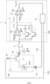
- FIG. 2 illustrates an electrical diagram of a first embodiment of the reading circuit 3 according to the invention connected to a ferroelectric CM ij memory cell with variable electrical polarization.
- the reading circuit 3 is connected to the second input/output node BL of the memory cell to be read CM ij through a reading activation switch i3.
- the i3 read activation switch allows the BL node to be isolated from the read circuit 3 if necessary.
- the memory cell CM ij has the same architecture described previously.
- the parasitic capacitance C BL seen by the second input/output node BL is represented here in order to facilitate understanding of the invention.
- the reading circuit 3 comprises a capacitive transimpedance amplifier stage 31 (translation of the term into English Capacitive Trans-Impedance Amplifier); a comparator 32, a sequencer circuit 33 and a reset switch i1.
- the capacitive transimpedance amplifier stage 31 comprises an operational amplifier AO associated with a capacitive feedback impedance (CCR).
- the operational amplifier AO has a first input e1_ao connected to the second input/output node BL of the associated memory cell; a second input e2_ao for receiving a first reference signal VREF1; and an s1_ao output for providing an analog Vs1_ao read signal.
- the capacitive feedback impedance CCR is mounted between the output s1_ao and the first input e1_ao of the operational amplifier. This type of assembly makes it possible to carry out a direct reading of the quantity of charges contained in the elementary component NVM and not a reading of a voltage variation on the BL node. This assembly thus makes it possible to carry out a reading operation whose precision is independent of the parasitic capacitance C BL .
- the capacitive feedback impedance CCR has the function of converting the quantity of charges supplied by the elementary component NVM (similar to a capacitive element) into an electrical voltage applied between the output s1_ao and the input e1_ao during a switching operation. reading.
- the read circuit comprises a first feedback activation switch i2 between the capacitive feedback impedance CCR and the first input e1_ao of the operational amplifier.
- the comparator 32 has a first input e1_cmp connected to the output s1_ao of the operational amplifier; a second input e2_cmp for receiving a second reference signal VREF2; and an output s1_cmp for providing a digital reading signal Vs1_cmp resulting from the comparison of the analog reading signal Vs1_ao with the second reference signal VREF2.
- the comparator 32 and the operational amplifier AO are each biased by a supply voltage VDD and the electrical ground GND.
- the action of sequencer 33 on the VSL and WL signals will be detailed in a later section.
- the sequencer 33 makes it possible to set up a feedback loop allowing a rewriting operation to be carried out by the reading circuit itself. This makes it possible to overcome destructive reading problems without making the circuit more complex.
- the sequencer action allows rewriting to be performed without transferring the data to external buffers.
- the reset switch i1 is connected between the output s1_ao and the first input e1_ao of the operational amplifier.
- switch reset i1 When switch reset i1 is in the on state, the capacitive feedback impedance CCR is discharged. This discharge also induces the resetting of the analog read signal Vs1_ao to a potential equal to that of the first reference signal VREF1.
- closing the reset switch i1 makes it possible to dissipate the cumulative charges on the second input/output node BL due to leakage currents. Indeed, for advanced technological nodes, there is an increase in leakage currents coming from the selection transistors connected to the second input/output node BL. These leakage currents lead to an accumulation of charges at the level of the parasitic capacitance C BL . This induces potential fluctuations at the second input/output node BL. Hence the specific interest of the reset switch i1 in this scenario.
- the switches i1, i2 and i3 are controlled by control means not shown to simplify the illustration.
- the switches i1, i2 and i3 are made by CMOS transistors as an example.
- the reading circuit 3 is configured to carry out the following steps:
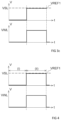
- the first step (i) is a reset step obtained by the configuration illustrated by the figure 3a .
- Reset switch i1, feedback enable switch i2 and read enable switch i3 are closed.
- the sequencer 33 generates a selection signal VWL so as to put the selection transistor T1 in a blocking state.
- the sequencer 33 generates a write and read control signal VSL on the first input/output node SL equal to the electrical ground.
- This step (i) makes it possible to discharge the capacitive feedback impedance CCR and to polarize the first input e1_ao of the operational amplifier to the first reference signal VREF1.
- the second step (ii) is a reading step obtained by the configuration illustrated by the figure 3c .
- FIG 3c illustrates a flowchart of the VSL and VWL signals supplied by the sequencer 33 during a reading step ii).
- Reset switch i1 is open and switches i2 and i3 are closed (on state).
- the sequencer 33 is configured during this step to apply a selection signal VWL making it possible to put the selection transistor T1 in the on state (a rising edge in the case of an NMOS is illustrated here). This results in the creation of a connection path between the elementary component NVM and the capacitive feedback element CCR.
- sequencer 33 is configured to apply a positive read control signal VSL to the first input/output node SL. This results in the application of an almost zero potential difference across the elementary component NVM.
- the combination of the almost zero voltage across the elementary component NVM and its connection with the capacitive feedback element CCR induces a transfer of the charges previously stored in the elementary component NVM to the capacitive feedback element CCR.
- the amount of charge transferred depends on the logic state previously stored in memory CM ij .
- the value of the electrical voltage across the capacitive feedback element CCR depends on the quantity of charges supplied by elementary component NVM to the capacitive feedback element CCR. This induces a variation in the analog output signal Vs1_ao which passes to VREF1-VCCR.
- Vs1_ao VREF1-VCCR ⁇ VREF2 with VCCR of the order of a few hundred millivolts.
- Vs1_cmp VDD corresponding to a high logic level.
- the reading circuit 3 thus makes it possible to carry out a reading operation in the field of loads independent of the value of the parasitic capacitance C BL .
- the third step (iii) consists of rewriting the logical data previously read by the reading circuit 3.
- the rewriting operation is only required in the case where the data read corresponds to a high logic state.
- FIG. 5b illustrates an electrical diagram of a first configuration of the reading circuit 3 according to the invention during a rewriting step.
- the feedback activation switch i2 is kept closed during the writing step so as to repatriate the charges accumulated in the feedback capacitor CCR to the elementary component NVM.
- the charges have not been evacuated downstream of the capacitive transimpedance amplifier 31.
- the charges transmitted during reading are repatriated to the memory cell for rewriting the information with lower energy consumption than in the solution of the 'state of the art.
- FIG. 5c illustrates an electrical diagram of a second configuration of the reading circuit according to the invention during a rewriting step.
- the feedback activation switch i2 is open. This makes it possible to rewrite the memory cell using the potential difference applied between the SL and BL nodes while keeping a copy of the information read in the capacitive feedback impedance CCR.
- FIG. 5d illustrates an electrical diagram of a third configuration of the reading circuit according to the invention during a rewriting step.
- feedback enable switch i2 is open and reset switch i1 is closed.
- This makes it possible to rewrite the memory cell using the potential difference applied between the SL and BL nodes.
- This configuration has a particular advantage in the case where the bit line connected to the node BL is capacitive so as to present a potential not equal to the voltage of VREF1.
- the storage circuit 1 comprises a matrix of memory cells 2 and a plurality of read circuits 3.
- the matrix of memory cells comprises N rows and M columns.
- the memory cells CM ij belonging to the same column C j have first input/output nodes SL interconnected via a common source line (SL n for column C n ).
- the memory cells CM ij belonging to the same column C j present second input/output nodes BL interconnected via a common bit line (BL n for column C n ).
- the memory cells CM ij belonging to the same row L i have selection nodes WL interconnected via a common word line (WL n for the column L n ). It is then a matrix structure with the bit lines BL j and the source lines SL j parallel in a first direction.
- the word lines WL i are orthogonal to said first direction.
- the storage circuit 1 comprises at the foot of each column C j a reading circuit 3 according to the invention connected to the bit line BL j of said column.
- Each reading circuit 3 acts via its feedback loop on the memory cells CM ij belonging to the same column C j to carry out non-destructive reading.
- This configuration makes it possible to write and read a target memory cell CM ij without disturbing the adjacent memory cells in row or column. To do this, it is sufficient to polarize the bit lines BL j of the memory cells adjacent to the electrical ground GND. In addition, this configuration makes it possible to carry out parallel writes/reads of all the memory cells belonging to the same line L i . This parallelization is possible thanks to the independence between the bit lines BL j and the source lines SL j of this set of memory cells.
- the storage circuit 1 further comprises writing means not shown for the sake of simplification.
- the writing means are distinct from the reading circuit according to the invention.
- the writing means are configured to carry out data writing operations and do not intervene in the rewriting operations in response to a destructive reading previously illustrated in the context of the invention
- FIG. 6b illustrates a second embodiment of the storage circuit 1 according to the invention.
- the second embodiment differs from the first by the different orientation of the source lines SL n , SL n-1 , SL n+1 .
- the source lines are common to the memory cells CM ij belonging to the same line L i .
- the source lines SL i extend in a direction orthogonal to that of the bit lines BL j and parallel to that of the word lines WL i .
- This configuration is compatible with the invention provided that inhibition signals are applied to the bit lines BL j of the other columns C j different from that of the memory cell selected for a read operation. That makes it possible to avoid disturbances in the state of the memory cells CM ij belonging to the same line of the target memory cell during its reading.
- the data storage circuit 1 comprises memory cells of the variable conductive filament resistive memory type (OxRAM for example).
- the resistive memory cells with a variable conductive filament can be co-integrated with the ferroelectric memory cells in the same matrix 2.
- the resistive memory cells with a variable conductive filament can be integrated in a second matrix distinct from the matrix 2.
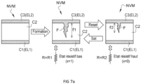
- FIG. 7a illustrates an elementary NVM component of a resistive memory cell with a variable conductive filament compatible with the invention. Resistive operation with variable conductive filament requires the formation of a conductive filament F through at least part of the electrically insulating central layer C2.
- the elementary component NVM is a MIM type structure (metal, insulator, metal) presenting an infinite resistance between the two electrodes EL1 and EL2.
- MIM type structure metal, insulator, metal
- the filament F is formed by the upper electrode EL2 through at least part of the volume of the central layer C2.
- the formation of the filament makes it possible to obtain a variable resistance by modulating the length l of the conductive filament formed.
- an electrical forming voltage is applied to the upper electrode EL2.
- the formation electrical voltage has a sufficiently high amplitude and/or duration to cause the generation of oxygen vacancies in the central layer C2.
- the applied electrical formation voltage must exceed a predetermined value so as to extract oxygen ions from the crystal lattice of the central metal oxide layer which will migrate towards the upper electrode EL2 thus forming a conductive filament F through the layer central consisting of oxygen vacancies.
- the behavior of a resistive element is obtained at a variable resistance R depending on the length l of the conductive filament F.
- a positive electrical voltage is applied to the lower electrode EL1
- the resistance of the resistive element increases.
- a positive electrical voltage is applied to the upper electrode EL2
- the length of the conductive filament F increases by the same mechanism described for the wire forming operation.
- the resistance of the resistive element decreases.
- a low resistive state and a SET type write operation is
- Reading a resistive NVM memory component involves estimating the resistance between the top electrode and the bottom electrode and comparing it to a threshold value to determine whether the resistive state is a high or low state.
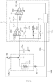
- FIG. 7b illustrates an electrical diagram of a second embodiment of the reading circuit 3 according to the invention connected to a resistive memory cell with a variable conductive filament.
- FIG. 7c illustrates a flowchart of the control signals of the resistive memory cell during reading of a memory cell by the reading circuit according to the invention.
- the elementary component NVM behaves like a resistor.
- the read circuit 3 further comprises a resistive feedback impedance RCR mounted between the output s1_ao and the first input e1_ao of the operational amplifier AO.
- the read circuit 3 comprises a second feedback activation switch i4 between the resistive feedback impedance RCR and the first input e1_ao of the operational amplifier A0.
- the second feedback activation switch i4 is in the on state and the first feedback activation switch i2 is in the off state.
- the sequencer 33 is configured to apply a positive read control signal VSL to the first input/output node SL with the transistor T1 in the on state.
- the amplitude of the positive reading control signal VSL is greater than that of the first reference signal VREF1 (potential of the second node BL).
- the elementary resistive component NVM is then subjected to a non-zero potential difference. This results in the circulation of an electric current l1 through the resistance NVM and the resistive feedback impedance RCR.
- the intensity of the current l1 depends on the resistive state of the filament of the elementary component NVM. This induces a variation of the voltage VRCR across the resistive feedback impedance RCR which depends on the intensity of the current l1. This results in a variation of the electric potential at the output node s1_ao of the operational amplifier AO.
- This voltage variation is an image of the resistive state of the elementary component NVM according to the logical content stored in said component. Reading an elementary NVM component does not destroy the logical content of the memory cell. There is no need for a rewrite step in this case.
Applications Claiming Priority (1)
| Application Number | Priority Date | Filing Date | Title |
|---|---|---|---|
| FR2209851A FR3140198A1 (fr) | 2022-09-28 | 2022-09-28 | Circuit de lecture non-destructive de mémoires ferroélectriques |
Publications (1)
| Publication Number | Publication Date |
|---|---|
| EP4345820A1 true EP4345820A1 (de) | 2024-04-03 |
Family
ID=85018136
Family Applications (1)
| Application Number | Title | Priority Date | Filing Date |
|---|---|---|---|
| EP23192686.6A Pending EP4345820A1 (de) | 2022-09-28 | 2023-08-22 | Schaltung zum zerstörungsfreien auslesen ferroelektrischer speicher |
Country Status (3)
| Country | Link |
|---|---|
| US (1) | US20240105246A1 (de) |
| EP (1) | EP4345820A1 (de) |
| FR (1) | FR3140198A1 (de) |
Citations (1)
| Publication number | Priority date | Publication date | Assignee | Title |
|---|---|---|---|---|
| US20210020222A1 (en) * | 2019-07-17 | 2021-01-21 | Micron Technology, Inc. | Ferroelectric memory cell with access line disturbance mitigation |
-
2022
- 2022-09-28 FR FR2209851A patent/FR3140198A1/fr active Pending
-
2023
- 2023-08-22 EP EP23192686.6A patent/EP4345820A1/de active Pending
- 2023-08-23 US US18/237,333 patent/US20240105246A1/en active Pending
Patent Citations (1)
| Publication number | Priority date | Publication date | Assignee | Title |
|---|---|---|---|---|
| US20210020222A1 (en) * | 2019-07-17 | 2021-01-21 | Micron Technology, Inc. | Ferroelectric memory cell with access line disturbance mitigation |
Also Published As
| Publication number | Publication date |
|---|---|
| FR3140198A1 (fr) | 2024-03-29 |
| US20240105246A1 (en) | 2024-03-28 |
Similar Documents
| Publication | Publication Date | Title |
|---|---|---|
| EP2047476B1 (de) | Ladungszurückhaltungsschaltung zur zeitmessung | |
| EP2050098B1 (de) | Eeprom-ladungserhaltungsschaltung für zeitmessung | |
| EP2047475B1 (de) | Schaltung zur auslesung eines ladungszurückhaltungselements zur zeitmessung | |
| JP2019525377A (ja) | メモリアレイのフルバイアスセンシング | |
| KR102436911B1 (ko) | 메모리 셀을 예비충전하기 위한 기법 | |
| EP2047477B1 (de) | Programmierung einer ladungszurückhaltungsschaltung zur zeitmessung | |
| EP2240956B1 (de) | EEPROM-Zelle mit Ladungsverlust und Herstellungsverfahren derselben, sowie Verfahren zum Messen einer Zeit-Information | |
| JPS5858759B2 (ja) | メモリ装置 | |
| FR2957449A1 (fr) | Micro-amplificateur de lecture pour memoire | |
| EP3496101A1 (de) | Sram-speicher mit schneller löschfunktion | |
| FR2828328A1 (fr) | Memoire semi-conductrice comprenant un circuit de compensation de cellule memoire defectueuse | |
| EP3373303A1 (de) | Tfet-speicherlatch ohne aktualisierung | |
| EP4345820A1 (de) | Schaltung zum zerstörungsfreien auslesen ferroelektrischer speicher | |
| EP0902437A1 (de) | Hochspannungsgeneratorschaltung zum Programmieren oder Löschen eines Speichers | |
| EP2977988B1 (de) | Nicht-flüchtiger speicher mit programmierbarem widerstand | |
| FR2735896A1 (fr) | Memoire eeprom programmable et effacable par effet de fowler-nordheim | |
| FR3044460A1 (fr) | Amplificateur de lecture pour memoire, en particulier une memoire eeprom | |
| AU641205B2 (en) | Ferroelectric memory structure | |
| EP4345821A1 (de) | In eine datenspeicherschaltung integrierte logische datenverarbeitungsschaltung | |
| FR3118267A1 (fr) | Lecture différentielle de mémoire rram à faible consommation | |
| EP3594951B1 (de) | Sram-/rom-speicher, der durch substratvorspannung rekonfigurierbar ist | |
| FR3130447A1 (fr) | Mémoires non volatiles à technologies mixtes OxRAM/FeRAM | |
| EP0669622B1 (de) | Vorspannungsschaltung für einen Transistor in einer Speicherzelle | |
| EP0996064B1 (de) | Einmalig programmierbare Speicherzelle | |
| EP4016531A1 (de) | Speicher mit einer matrix aus resistiven speicherzellen und entsprechendes schnittstellenverbindungsverfahren |
Legal Events
| Date | Code | Title | Description |
|---|---|---|---|
| PUAI | Public reference made under article 153(3) epc to a published international application that has entered the european phase |
Free format text: ORIGINAL CODE: 0009012 |
|
| STAA | Information on the status of an ep patent application or granted ep patent |
Free format text: STATUS: REQUEST FOR EXAMINATION WAS MADE |
|
| 17P | Request for examination filed |
Effective date: 20230822 |
|
| AK | Designated contracting states |
Kind code of ref document: A1 Designated state(s): AL AT BE BG CH CY CZ DE DK EE ES FI FR GB GR HR HU IE IS IT LI LT LU LV MC ME MK MT NL NO PL PT RO RS SE SI SK SM TR |