EP4345516A1 - Unidirectional perspective film, single-sided mirror and preparation method therefor, and electronic device - Google Patents
Unidirectional perspective film, single-sided mirror and preparation method therefor, and electronic device Download PDFInfo
- Publication number
- EP4345516A1 EP4345516A1 EP22860491.4A EP22860491A EP4345516A1 EP 4345516 A1 EP4345516 A1 EP 4345516A1 EP 22860491 A EP22860491 A EP 22860491A EP 4345516 A1 EP4345516 A1 EP 4345516A1
- Authority
- EP
- European Patent Office
- Prior art keywords
- oxide layer
- niobium
- silicon oxide
- thickness
- power supply
- Prior art date
- Legal status (The legal status is an assumption and is not a legal conclusion. Google has not performed a legal analysis and makes no representation as to the accuracy of the status listed.)
- Pending
Links
Images


Classifications
-
- G—PHYSICS
- G02—OPTICS
- G02B—OPTICAL ELEMENTS, SYSTEMS OR APPARATUS
- G02B5/00—Optical elements other than lenses
- G02B5/08—Mirrors
- G02B5/0816—Multilayer mirrors, i.e. having two or more reflecting layers
-
- C—CHEMISTRY; METALLURGY
- C23—COATING METALLIC MATERIAL; COATING MATERIAL WITH METALLIC MATERIAL; CHEMICAL SURFACE TREATMENT; DIFFUSION TREATMENT OF METALLIC MATERIAL; COATING BY VACUUM EVAPORATION, BY SPUTTERING, BY ION IMPLANTATION OR BY CHEMICAL VAPOUR DEPOSITION, IN GENERAL; INHIBITING CORROSION OF METALLIC MATERIAL OR INCRUSTATION IN GENERAL
- C23C—COATING METALLIC MATERIAL; COATING MATERIAL WITH METALLIC MATERIAL; SURFACE TREATMENT OF METALLIC MATERIAL BY DIFFUSION INTO THE SURFACE, BY CHEMICAL CONVERSION OR SUBSTITUTION; COATING BY VACUUM EVAPORATION, BY SPUTTERING, BY ION IMPLANTATION OR BY CHEMICAL VAPOUR DEPOSITION, IN GENERAL
- C23C14/00—Coating by vacuum evaporation, by sputtering or by ion implantation of the coating forming material
- C23C14/0021—Reactive sputtering or evaporation
- C23C14/0036—Reactive sputtering
-
- C—CHEMISTRY; METALLURGY
- C23—COATING METALLIC MATERIAL; COATING MATERIAL WITH METALLIC MATERIAL; CHEMICAL SURFACE TREATMENT; DIFFUSION TREATMENT OF METALLIC MATERIAL; COATING BY VACUUM EVAPORATION, BY SPUTTERING, BY ION IMPLANTATION OR BY CHEMICAL VAPOUR DEPOSITION, IN GENERAL; INHIBITING CORROSION OF METALLIC MATERIAL OR INCRUSTATION IN GENERAL
- C23C—COATING METALLIC MATERIAL; COATING MATERIAL WITH METALLIC MATERIAL; SURFACE TREATMENT OF METALLIC MATERIAL BY DIFFUSION INTO THE SURFACE, BY CHEMICAL CONVERSION OR SUBSTITUTION; COATING BY VACUUM EVAPORATION, BY SPUTTERING, BY ION IMPLANTATION OR BY CHEMICAL VAPOUR DEPOSITION, IN GENERAL
- C23C14/00—Coating by vacuum evaporation, by sputtering or by ion implantation of the coating forming material
- C23C14/06—Coating by vacuum evaporation, by sputtering or by ion implantation of the coating forming material characterised by the coating material
- C23C14/08—Oxides
-
- C—CHEMISTRY; METALLURGY
- C23—COATING METALLIC MATERIAL; COATING MATERIAL WITH METALLIC MATERIAL; CHEMICAL SURFACE TREATMENT; DIFFUSION TREATMENT OF METALLIC MATERIAL; COATING BY VACUUM EVAPORATION, BY SPUTTERING, BY ION IMPLANTATION OR BY CHEMICAL VAPOUR DEPOSITION, IN GENERAL; INHIBITING CORROSION OF METALLIC MATERIAL OR INCRUSTATION IN GENERAL
- C23C—COATING METALLIC MATERIAL; COATING MATERIAL WITH METALLIC MATERIAL; SURFACE TREATMENT OF METALLIC MATERIAL BY DIFFUSION INTO THE SURFACE, BY CHEMICAL CONVERSION OR SUBSTITUTION; COATING BY VACUUM EVAPORATION, BY SPUTTERING, BY ION IMPLANTATION OR BY CHEMICAL VAPOUR DEPOSITION, IN GENERAL
- C23C14/00—Coating by vacuum evaporation, by sputtering or by ion implantation of the coating forming material
- C23C14/06—Coating by vacuum evaporation, by sputtering or by ion implantation of the coating forming material characterised by the coating material
- C23C14/10—Glass or silica
-
- C—CHEMISTRY; METALLURGY
- C23—COATING METALLIC MATERIAL; COATING MATERIAL WITH METALLIC MATERIAL; CHEMICAL SURFACE TREATMENT; DIFFUSION TREATMENT OF METALLIC MATERIAL; COATING BY VACUUM EVAPORATION, BY SPUTTERING, BY ION IMPLANTATION OR BY CHEMICAL VAPOUR DEPOSITION, IN GENERAL; INHIBITING CORROSION OF METALLIC MATERIAL OR INCRUSTATION IN GENERAL
- C23C—COATING METALLIC MATERIAL; COATING MATERIAL WITH METALLIC MATERIAL; SURFACE TREATMENT OF METALLIC MATERIAL BY DIFFUSION INTO THE SURFACE, BY CHEMICAL CONVERSION OR SUBSTITUTION; COATING BY VACUUM EVAPORATION, BY SPUTTERING, BY ION IMPLANTATION OR BY CHEMICAL VAPOUR DEPOSITION, IN GENERAL
- C23C14/00—Coating by vacuum evaporation, by sputtering or by ion implantation of the coating forming material
- C23C14/06—Coating by vacuum evaporation, by sputtering or by ion implantation of the coating forming material characterised by the coating material
- C23C14/14—Metallic material, boron or silicon
- C23C14/20—Metallic material, boron or silicon on organic substrates
-
- C—CHEMISTRY; METALLURGY
- C23—COATING METALLIC MATERIAL; COATING MATERIAL WITH METALLIC MATERIAL; CHEMICAL SURFACE TREATMENT; DIFFUSION TREATMENT OF METALLIC MATERIAL; COATING BY VACUUM EVAPORATION, BY SPUTTERING, BY ION IMPLANTATION OR BY CHEMICAL VAPOUR DEPOSITION, IN GENERAL; INHIBITING CORROSION OF METALLIC MATERIAL OR INCRUSTATION IN GENERAL
- C23C—COATING METALLIC MATERIAL; COATING MATERIAL WITH METALLIC MATERIAL; SURFACE TREATMENT OF METALLIC MATERIAL BY DIFFUSION INTO THE SURFACE, BY CHEMICAL CONVERSION OR SUBSTITUTION; COATING BY VACUUM EVAPORATION, BY SPUTTERING, BY ION IMPLANTATION OR BY CHEMICAL VAPOUR DEPOSITION, IN GENERAL
- C23C14/00—Coating by vacuum evaporation, by sputtering or by ion implantation of the coating forming material
- C23C14/22—Coating by vacuum evaporation, by sputtering or by ion implantation of the coating forming material characterised by the process of coating
- C23C14/34—Sputtering
-
- G—PHYSICS
- G02—OPTICS
- G02B—OPTICAL ELEMENTS, SYSTEMS OR APPARATUS
- G02B1/00—Optical elements characterised by the material of which they are made; Optical coatings for optical elements
- G02B1/10—Optical coatings produced by application to, or surface treatment of, optical elements
- G02B1/11—Anti-reflection coatings
- G02B1/113—Anti-reflection coatings using inorganic layer materials only
- G02B1/115—Multilayers
-
- G—PHYSICS
- G02—OPTICS
- G02B—OPTICAL ELEMENTS, SYSTEMS OR APPARATUS
- G02B5/00—Optical elements other than lenses
- G02B5/08—Mirrors
-
- G—PHYSICS
- G02—OPTICS
- G02B—OPTICAL ELEMENTS, SYSTEMS OR APPARATUS
- G02B5/00—Optical elements other than lenses
- G02B5/08—Mirrors
- G02B5/0816—Multilayer mirrors, i.e. having two or more reflecting layers
- G02B5/085—Multilayer mirrors, i.e. having two or more reflecting layers at least one of the reflecting layers comprising metal
- G02B5/0858—Multilayer mirrors, i.e. having two or more reflecting layers at least one of the reflecting layers comprising metal the reflecting layers comprising a single metallic layer with one or more dielectric layers
Definitions
- the present disclosure relates to the technical field of optics, and more specifically, to a unidirectional perspective film, a single-sided mirror and a method for preparing the same, and an electronic device.
- a single-sided mirror is a type of special coated glass, where a side is a glass mirror face (outer side), which can reflect light, has a function similar to that of an ordinary mirror, and has a mirror face effect; and another side (inner side), from which a scene outside the glass can be seen, has a perspective effect, that is, the inner side of the glass cannot be seen from the outer side of the glass, but from the inner side of the glass, a situation outside the glass can be seen.
- the single-sided mirror is applicable to sites such as prisons, interrogation rooms of public security bureaus, procuratorates, and courts, psychiatric hospitals, research laboratories of university research organizations, and large conference rooms.
- the present disclosure provides a unidirectional perspective film.
- the unidirectional perspective film is low in production cost and stable in performance, and has a good single-sided perspective effect.
- the unidirectional perspective film is diverse in color, and meets marketization requirements.
- the present disclosure further provides a single-sided mirror and a method for preparing the same, and an electronic device.
- a unidirectional perspective film including a first niobium oxide layer, a first silicon oxide layer, an absorption layer, a second niobium oxide layer, and a second silicon oxide layer that are sequentially arranged.
- the absorption layer has a thickness ranging from 8 nm to 20 nm.
- the absorption layer includes one or more of silicon, indium, niobium, titanium, and chromium.
- each of the first niobium oxide layer and the second niobium oxide layer has a thickness ranging from 10 nm to 120 nm.
- each of the first silicon oxide layer and the second silicon oxide layer has a thickness ranging from 10 nm to 160 nm.
- the first niobium oxide layer has a thickness ranging from 30 nm to 60 nm.
- the first silicon oxide layer has a thickness ranging from 90 nm to 110 nm.
- the second niobium oxide layer has a thickness ranging from 60 nm to 110 nm.
- the second silicon oxide layer has a thickness ranging from 50 nm to 90 nm.
- the unidirectional perspective film has a visible light transmission rate ranging from 10% to 25%.
- an absolute value of a difference between visible light reflection rates of two side surfaces of the unidirectional perspective film is greater than or equal to 15%.
- the first niobium oxide layer and the first silicon oxide layer form a reflection-enhancing layer, so that a surface (Ri face) of the unidirectional perspective film close to a side of the first niobium oxide layer has a high reflection rate, to form a mirror face effect; and the second niobium oxide layer and the second silicon oxide layer form a reflection-reducing layer, so that a surface (R 2 face) of the unidirectional perspective film close to a side of the second silicon oxide layer has a low reflection rate, to form a perspective effect.
- the absorption layer can absorb part of light. When the absorption layer has a thickness ranging from 8 nm to 20 nm, it can be ensured that the R 2 face cannot be seen from the R 1 face and the R 1 face can be seen from the R 2 face.
- the present disclosure provides a single-sided mirror, including a substrate and the unidirectional perspective film according to the first aspect of the present disclosure arranged on a surface of the substrate.
- the substrate is arranged on a surface of the first niobium oxide layer.
- the substrate includes a transparent substrate.
- the transparent substrate includes one or more of glass, an acrylic plate, an anti-explosion film, a release film, and polyethylene terephthalate (PET).
- PET polyethylene terephthalate
- the single-sided mirror provided in the second aspect of the present disclosure has a good unidirectional perspective effect, is low in cost and diverse in color, and is widely applied.
- the present disclosure provides a method for preparing a single-sided mirror, including:
- the absorption layer includes one or more of silicon, indium, niobium, titanium, and chromium; the absorption layer has a thickness ranging from 8 nm to 20 nm.
- the present disclosure provides an electronic device, including the unidirectional perspective film according to the first aspect of the present disclosure or the single-sided mirror according to the second aspect of the present disclosure.
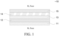
- FIG. 1 is a schematic diagram of a structure of a unidirectional perspective film according to an embodiment of the present disclosure.
- the unidirectional perspective film includes a first niobium oxide layer 11, a first silicon oxide layer 12, an absorption layer 13, a second niobium oxide layer 14, and a second silicon oxide layer 15 that are sequentially arranged.
- an outer side of the unidirectional perspective film refers to a side of the first niobium oxide layer 11; and an inner side of the unidirectional perspective film refers to a side of the second silicon oxide layer 15.
- an outer side surface (Ri face) of the unidirectional perspective film is the first niobium oxide layer, and no half-wave loss is generated when light from the outer side face passes through the first niobium oxide layer to the first silicon oxide layer, so that reflection of the light is enhanced, and the outer side of the unidirectional perspective film presents a mirror face effect; and an inner side surface (R 2 face) of the unidirectional perspective film is the second silicon oxide layer, and half-wave loss is generated when light from the inner side face passes through the second silicon oxide layer to the second niobium oxide layer, so that reflection of the light is reduced, and the inner side of the unidirectional perspective film presents a perspective effect.
- the unidirectional perspective film is prepared from niobium oxide and silicon oxide, which greatly reduces production costs and facilitates product promotion.
- the absorption layer may absorb part of light, so that the unidirectional perspective film has a transmission rate falling within a proper range.
- the absorption layer includes one or more of silicon, indium, niobium, titanium, and chromium.
- the absorption layer has a thickness ranging from 8 nm to 20 nm. Further, the absorption layer has a thickness ranging from 15 nm to 20 nm. The thickness of the absorption layer may be specifically, but is not limited to, 8 nm, 10 nm, 12 nm, 15 nm, 17 nm, or 20 nm.
- a large thickness of the absorption layer indicates a large light absorption amount and a small transmission rate of the unidirectional perspective film.
- a small thickness of the absorption layer indicates a small light absorption amount and a large transmission rate of the unidirectional perspective film.
- the absorption layer can well collaborate with the first niobium oxide layer, the first silicon oxide layer, the second niobium oxide layer, and the second silicon oxide layer, to ensure that the outer side of the unidirectional perspective film presents the mirror face effect and the inner side of the unidirectional perspective film presents the perspective effect.
- the unidirectional perspective film has a visible light transmission rate ranging from 10% to 25%.
- the visible light transmission rate of the unidirectional perspective film may be specifically, but is not limited to, 10%, 15%, 18%, 20%, 22%, or 25%.
- each of the first niobium oxide layer and the second niobium oxide layer has a thickness ranging from 10 nm to 120 nm.
- the thickness of each of the first niobium oxide layer and the second niobium oxide layer may be specifically, but is not limited to, 10 nm, 30 nm, 40 nm, 50 nm, 55 nm, 60 nm, 80 nm, 90 nm, 100 nm, or 120 nm.
- each of the first silicon oxide layer and the second silicon oxide layer has a thickness ranging from 10 nm to 160 nm.
- each of the first silicon oxide layer and the second silicon oxide layer may be specifically, but is not limited to, 10 nm, 30 nm, 50 nm, 70 nm, 80 nm, 90 nm, 100 nm, 110 nm, 120 nm, or 160 nm.
- the thicknesses of the first niobium oxide layer and, the second niobium oxide layer, the first silicon oxide layer, and the second silicon oxide layer are controlled to fall within the foregoing ranges, it can be ensured that the unidirectional perspective film has good structural stability and is not prone to fall off. In addition, preparation costs of the unidirectional perspective film are low, to facilitate product marketization.
- the unidirectional perspective effect of the unidirectional perspective film can be optimized, the reflection rate of the outer side of the unidirectional perspective film can be enhanced, and the reflection rate of the inner side of the unidirectional perspective film can be reduced, to achieve a good visual contrast effect with a side being a mirror face and a side being a perspective face.
- a side being a mirror face and a side being a perspective face.
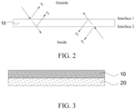
- r 1 is an amplitude reflection coefficient of outside light generated on an interface 1
- r 2 is an amplitude reflection coefficient of outside light generated on an interface 2
- r 3 is an amplitude reflection coefficient of inside light generated on the interface 2
- r 4 is an amplitude reflection coefficient of inside light generated on the interface 1.
- the reflection rate of the unidirectional perspective film on the interface 1 is Ri
- and R 2
- r 1 (N 0 -N 1 )/(N 0 +N 1 )
- r 2 (N 1 -N 2 )/(N 1 +N 2 )*e(-2 ⁇ )
- r3 (N 0 -N 2 )/(N 0 +N 2 )
- r 4 (N 2 -N 1 )/(N 1 +N 2 )*e(-2 ⁇ )
- ⁇ 2 ⁇ *N*D/ ⁇
- N 0 represents a refractive index of an incident medium
- N 1 represents a refractive index of silicon dioxide
- N 2 represents a refractive index of niobium oxide
- ⁇ represents a phase film thickness of the unidirectional perspective film
- D represents a physical film thickness of the unidirectional perspective film
- ⁇ represents a wavelength of light.
- an optical path difference of the light between layers of interfaces is an even multiple of a quarter wavelength
- reflection of the light may be enhanced; or when an optical path difference of the light between layers of interfaces is an odd multiple of a quarter wavelength, reflection of the light may be reduced.
- the outer side face of the single-sided perspective film may have a high reflection rate; and when the second niobium oxide layer has a thickness ranging from 60 nm to 110 nm and the second silicon oxide layer has a thickness ranging from 50 nm to 90 nm, the inner side face of the single-sided perspective film may have a low reflection rate.
- a ratio of the thickness of the first niobium oxide layer to that of the first silicon oxide layer is 1:(1.5 to 3.5), and a ratio of the thickness of the second niobium oxide layer to that of the second silicon oxide layer is 1:(0.5 to 1.5).
- the ratio of the thickness of the first niobium oxide layer to that of the first silicon oxide layer may be specifically, but is not limited to, 1:1.5, 1:2, 1:2.5, or 1:3.5, and the ratio of the thickness of the second niobium oxide layer to that of the second silicon oxide layer may be specifically, but is not limited to, 1:0.5, 1:0.7, 1:1, or 1:1.5.
- an absolute value of a difference between visible light reflection rates of two side surfaces of the unidirectional perspective film is greater than or equal to 15%.
- the absolute value of the difference between the visible light reflection rates of the two side surfaces of the unidirectional perspective film may be specifically, but is not limited to, 15%, 20%, 25%, 30%, 35%, or 40%.
- a larger difference between the visible light reflection rates of the two side surfaces of the unidirectional perspective film indicates a better single-sided perspective effect and a more significant visual difference.
- the thickness relationship between the layers of the unidirectional perspective film also affects the color of the film. Specifically, by adjusting the thicknesses of the layers, the reflection rate of the unidirectional perspective film for the visible light can be changed. Because the unidirectional perspective film has different reflection rates for light in different wavebands, the unidirectional perspective film can present different colors.
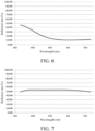
- FIG. 3 is a schematic diagram of a structure of a single-sided mirror according to an embodiment of the present disclosure, where the single-sided mirror includes a substrate 20 and a unidirectional perspective film 10 arranged on a surface of the substrate.
- the substrate includes a transparent substrate.
- the substrate includes one or more of glass and a polymeric transparent substrate, where the polymeric transparent substrate includes one or more of polyethylene terephthalate (PET), an acrylic plate, an anti-explosion film, and a release film.
- PET polyethylene terephthalate
- the unidirectional perspective film may be arranged on any surface of the substrate.
- the substrate is arranged on an outer side (Ri face) of the unidirectional perspective film, that is, the substrate is adjacent to the first niobium oxide layer in the unidirectional perspective film, and the foregoing position arrangement can ensure that the single-sided mirror has a good single-sided perspective effect.
- the present disclosure further provides a method for preparing a single-sided mirror, including the following steps:
- a substrate is provided, and a first niobium oxide layer, a first silicon oxide layer, an absorption layer, a second niobium oxide layer, and a second silicon oxide layer are deposited sequentially on a surface of the substrate to obtain the single-sided mirror.
- the first niobium oxide layer, the first silicon oxide layer, the absorption layer, the second niobium oxide layer, and the second silicon oxide layer are prepared using a sputtering method. Specifically, for the first niobium oxide layer and the second niobium oxide layer, argon and oxygen are fed into a sputtering machine, a niobium target is bombarded through the argon, sputtered niobium reacts with the oxygen to form niobium oxide, and the niobium oxide is deposited simultaneously to form niobium oxide layers.
- argon and oxygen are fed into the sputtering machine, a silicon target is bombarded through the argon, sputtered silicon reacts with the oxygen to form silicon oxide, and the silicon oxide is deposited simultaneously to form silicon oxide layers.
- the absorption layer includes one or more of silicon, indium, niobium, titanium, and chromium.
- the absorption layer is prepared by bombarding a corresponding target material through argon.
- the absorption layer is a silicon layer
- the silicon layer is obtained by bombarding a silicon target through argon and depositing silicon simultaneously.
- a method for preparing a single-sided mirror is as follows:
- a substrate is provided, the substrate placed in a sputtering machine, and a platform furnace chamber is vacuumized.
- Argon is fed into the platform furnace chamber, an ion source is opened after the gas is stable, and ion cleaning is performed on surfaces of the substrate and a target material, where ICP power of the ion source ranges from 0.5 kw to 5 kw, a vacuum degree of the platform furnace chamber ranges from 1 ⁇ 10 -3 to 1 ⁇ 10 -2 Pa, and an ion cleaning time ranges from 1 min to 60 min.
- Argon is continuously fed, and oxygen starts to be fed, where a flow rate of the oxygen ranges from 200 sccm to 300 sccm; a sputtering power supply of a niobium target is started, where sputtering power ranges from 5 kw to 15 kw and a working pressure of a coating film ranges from 0.07 Pa to 1 Pa; and a first niobium oxide layer is deposited on the surface of the substrate, where the first niobium oxide layer has a thickness ranging from 10 nm to 120 nm.
- the sputtering power supply of the niobium target is turned off, argon and oxygen are continuously fed, and a sputtering power supply of a silicon target is turned on, where sputtering power ranges from 5 kw to 15 kw and a working pressure of a coating film ranges from 0.07 Pa to 1 Pa; and a first silicon oxide layer is deposited on a surface of the first niobium oxide layer, where the first silicon oxide layer has a thickness ranging from 10 nm to 160 nm.
- Oxygen is stopped from being fed, and a sputtering power supply of a target material at an absorption layer is turned on, where sputtering power ranges from 5 kw to 15 kw and a working pressure of a coating film ranges from 0.07 Pa to 1 Pa; and the absorption layer is deposited on a surface of the first silicon oxide layer, where the absorption layer has a thickness ranging from 8 nm to 20 nm.
- Argon is continuously fed, and oxygen begins to be fed, where a flow rate of the oxygen ranges from 200 sccm to 300 sccm; a sputtering power supply of a niobium target is started, where sputtering power ranges from 5 kw to 15 kw and a working pressure of a coating film ranges from 0.07 Pa to 1 Pa; and a second niobium oxide layer is deposited on the surface of the substrate, where the second niobium oxide layer has a thickness ranging from 10 nm to 120 nm.
- the sputtering power supply of the niobium target is turned off, argon and oxygen are continuously fed, and a sputtering power supply of a silicon target is turned on, where sputtering power ranges from 5 kw to 15 kw and a working pressure of a coating film ranges from 0.07 Pa to 1 Pa; and a second silicon oxide layer is deposited on a surface of the second niobium oxide layer, where the second silicon oxide layer has a thickness ranging from 10 nm to 160 nm. Then, an atomic mirror is obtained.
- the method for preparing an atomic mirror provided in the present disclosure is simple in process and high in production efficiency, and the prepared atomic mirror has high structural stability and has a good single-sided perspective effect.
- the present disclosure further provides an electronic device, including the unidirectional perspective film or the single-sided mirror according to the present disclosure.
- the electronic device includes a housing, and the housing includes a housing substrate and a unidirectional perspective film, where the housing substrate can provide an arrangement position and support for another structure of the electronic device, and the housing substrate may be a glass substrate or a polymeric transparent substrate.
- the unidirectional perspective film is arranged on a surface of the housing substrate, and a side of the unidirectional perspective film whose reflection rate is high is used as an appearance face of the housing toward the outside of the housing.
- a mirror face effect is presented on the appearance face of the housing, thereby blocking a product structure inside the housing.
- a light-emitting source may be arranged inside the housing, the light-emitting source may be an LED lamp or an organic light-emitting material, and by designing a shape of the light-emitting source and a color of emitted light, a specific pattern such as a product logo or a decorative motif may be formed.
- the single-sided mirror has a specific transmission rate.
- a pattern inside the housing can also be seen from the outside of the housing, but an area where no light is emitted inside the housing is still invisible, that is, a light-emitting pattern inside the housing can be seen from the appearance face of the housing, but the area where no light is emitted inside the housing is still a mirror face, thereby achieving a magic decorative effect.
- the electronic device includes a display screen assembly
- the display screen assembly includes a display panel and a unidirectional perspective film
- the unidirectional perspective film is arranged on a surface of the display panel.
- a side of the unidirectional perspective film whose reflection rate is high faces the outside of the display screen assembly.
- the display screen presents a mirror face effect; and when the display screen is on, pictures of the display screen can be normally displayed.
- the display screen assembly does not emit light (off), light on the outer side of the unidirectional perspective film is brighter, so that reflection of the light is strong, and the surface of the display screen has a mirror face effect; and when the display screen emits light (on), light on the inner side of the unidirectional perspective film is brighter, so that light transmitted from the display screen has high intensity, and content displayed by the display screen can be seen from the outside of the display screen, thereby implementing normal display when the display screen is on, and achieving a decorative effect of a mirror face when the display screen is off.
- the electronic device may be specifically a mobile phone, a computer, an e-cigarette, a smart band, a wearable device, or the like.
- a method for preparing a single-sided mirror includes: A glass substrate is provided, where the glass substrate has a thickness of 3 mm, and the glass substrate is ultrasonically cleaned using ethanol, then rinsed using deionized water, and dried in a vacuum environment.
- the glass substrate is placed on a workpiece turret of a sputtering machine, and a platform is vacuumized, to enable a pressure in a working chamber to be lower than 0.003 Pa.
- An ion source is opened, and argon is fed, where the argon has a flow rate of 280 sccm; and ion cleaning is performed on a surface of the glass substrate, where ICP power of the ion source is 0.7 kw, a vacuum degree is 0.8 Pa, and time is 5 min.
- Argon is continuously fed, oxygen starts to be fed, and a sputtering power supply of a niobium target is turned on, where power of the sputtering power supply is 8 kw; and a first niobium oxide layer is deposited on the surface of the glass substrate, where a working pressure of a coating film is 0.43 Pa, a coating time is 186s, and the first niobium oxide layer has a thickness of 56 nm.
- the niobium target is turned off, a gas source continuously supplies gas, and a sputtering power supply of a silicon target is turned on, where power of the sputtering power supply is 8 kw; and a first silicon oxide layer is deposited on a surface of the first niobium oxide layer, where a working pressure of a coating film is 0.43 Pa, a coating time is 327s, and the first silicon oxide layer has a thickness of 105 nm.
- Oxygen is turned off, and the silicon target is continuously turned on, where power of a sputtering power supply is 8 kw; and a silicon layer deposited on a surface of the first silicon oxide layer, where a working pressure of a coating film is 0.26 Pa, a coating time is 182s, and the silicon layer has a thickness of 18 nm.
- the sputtering power supply of the silicon target is turned off, oxygen is fed, and a sputtering power supply of a niobium target is turned on, where power of the sputtering power supply is 8 kw; and a second niobium oxide layer is deposited on a surface of the silicon layer, where a working pressure of a coating film is 0.43 Pa, a coating time is 340s, and the second niobium oxide layer has a thickness of 102 nm.
- the niobium target is turned off, the gas source continuously supplies gas, the sputtering power supply of the silicon target is turned on, where the power of the sputtering power supply is 8 kw; a second silicon oxide layer is deposited on a surface of the second niobium oxide layer, where a working pressure of a coating film is 0.43 Pa, a coating time is 183s, and the second silicon oxide layer has a thickness of 55 nm; and a unidirectional perspective film is formed, and a single-sided mirror is obtained, where a structure of the single-sided mirror is substrate /Nb 2 O 5 (56 nm)/SiO 2 (105 nm)/Si (18 nm)/Nb 2 O 5 (102 nm)/SiO 2 (55 nm).
- a method for preparing a single-sided mirror includes: A glass substrate is provided, where the glass substrate has a thickness of 3 mm, and the glass substrate is ultrasonically cleaned using ethanol, then rinsed using deionized water, and dried in a vacuum environment.
- the glass substrate is placed on a workpiece turret of a sputtering machine, and a platform is vacuumized, to enable a pressure in a working chamber to be lower than 0.003 Pa.
- An ion source is opened, and argon is fed, where the argon has a flow rate of 280 sccm; and ion cleaning is performed on a surface of the glass substrate, where ICP power of the ion source is 0.7 kw, a vacuum degree is 0.8 Pa, and time is 5 min.
- Argon is continuously fed, oxygen starts to be fed, and a sputtering power supply of a niobium target is turned on, where power of the sputtering power supply is 8 kw; and a first niobium oxide layer is deposited on the surface of the glass substrate, where a working pressure of a coating film is 0.45 Pa, a coating time is 106s, and the first niobium oxide layer has a thickness of 32 nm.
- the niobium target is turned off, a gas source continuously supplies gas, and a sputtering power supply of a silicon target is turned on, where power of the sputtering power supply is 8 kw; and a first silicon oxide layer is deposited on a surface of the first niobium oxide layer, where a working pressure of a coating film is 0.45 Pa, a coating time is 316s, and the first silicon oxide layer has a thickness of 95 nm.
- Oxygen is turned off, and an indium target is turned on, where power of a sputtering power supply is 8 kw; and an indium layer deposited on a surface of the first silicon oxide layer, where a working pressure of a coating film is 0.25 Pa, a coating time is 180s, and the indium layer has a thickness of 18 nm.
- the sputtering power supply of the indium target is turned off, oxygen is fed, and a sputtering power supply of a niobium target is turned on, where power of the sputtering power supply is 8 kw; and a second niobium oxide layer is deposited on a surface of the indium layer, where a working pressure of a coating film is 0.45 Pa, a coating time is 206s, and the second niobium oxide layer has a thickness of 62 nm.
- the niobium target is turned off, the gas source continuously supplies gas, the sputtering power supply of the silicon target is turned on, where the power of the sputtering power supply is 8 kw; a second silicon oxide layer is deposited on a surface of the second niobium oxide layer, where a working pressure of a coating film is 0.45 Pa, a coating time is 286s, and the second silicon oxide layer has a thickness of 86 nm; and a unidirectional perspective film is formed, and a single-sided mirror is obtained, where a structure of the single-sided mirror is substrate /Nb 2 O 5 (32 nm)/SiO 2 (95 nm)/In (18 nm)/Nb 2 O 5 (62 nm)/SiO 2 (86 nm).
- a method for preparing a single-sided mirror includes: A glass substrate is provided, where the glass substrate has a thickness of 3 mm, and the glass substrate is ultrasonically cleaned using ethanol, then rinsed using deionized water, and dried in a vacuum environment.
- the glass substrate is placed on a workpiece turret of a sputtering machine, and a platform is vacuumized, to enable a pressure in a working chamber to be lower than 0.003 Pa.
- An ion source is opened, and argon is fed, where the argon has a flow rate of 280 sccm; and ion cleaning is performed on a surface of the glass substrate, where ICP power of the ion source is 0.7 kw, a vacuum degree is 0.8 Pa, and time is 5 min.
- Argon is continuously fed, oxygen starts to be fed, and a sputtering power supply of a niobium target is turned on, where power of the sputtering power supply is 8 kw; and a first niobium oxide layer is deposited on the surface of the glass substrate, where a working pressure of a coating film is 0.45 Pa, a coating time is 127s, and the first niobium oxide layer has a thickness of 38 nm.
- the niobium target is turned off, a gas source continuously supplies gas, and a sputtering power supply of a silicon target is turned on, where power of the sputtering power supply is 8 kw; and a first silicon oxide layer is deposited on a surface of the first niobium oxide layer, where a working pressure of a coating film is 0.45 Pa, a coating time is 326s, and the first silicon oxide layer has a thickness of 98 nm.
- Oxygen is turned off, and the niobium target is turned on, where power of a sputtering power supply is 5 kw; and a niobium layer deposited on a surface of the first silicon oxide layer, where a working pressure of a coating film is 0.45 Pa, a coating time is 180s, and the film layer has a thickness of 18 nm.
- the sputtering power supply of the niobium target is turned off, oxygen is fed, and the sputtering power supply of the niobium target is turned on, where power of the sputtering power supply is 8 kw; and a second niobium oxide layer is deposited on a surface of the niobium layer, where a working pressure of a coating film is 0.45 Pa, a coating time is 217s, and the second niobium oxide layer has a thickness of 65 nm.
- the niobium target is turned off, the gas source continuously supplies gas, the sputtering power supply of the silicon target is turned on, where the power of the sputtering power supply is 8 kw; a second silicon oxide layer is deposited on a surface of the second niobium oxide layer, where a working pressure of a coating film is 0.45 Pa, a coating time is 206s, and the second silicon oxide layer has a thickness of 62 nm; and a unidirectional perspective film is formed, and a single-sided mirror is obtained, where a structure of the single-sided mirror is substrate /Nb 2 O 5 (38 nm)/SiO 2 (98 nm)/Nb (18 nm)/Nb 2 O 5 (65 nm)/SiO 2 (62 nm).
- a method for preparing a single-sided mirror includes: A glass substrate is provided, where the glass substrate has a thickness of 3 mm, and the glass substrate is ultrasonically cleaned using ethanol, then rinsed using deionized water, and dried in a vacuum environment.
- the glass substrate is placed on a workpiece turret of a sputtering machine, and a platform is vacuumized, to enable a pressure in a working chamber to be lower than 0.003 Pa.
- An ion source is opened, and argon is fed, where the argon has a flow rate of 280 sccm; and ion cleaning is performed on a surface of the glass substrate, where ICP power of the ion source is 0.7 kw, a vacuum degree is 0.8 Pa, and time is 5 min.
- Argon is continuously fed, oxygen starts to be fed, and a sputtering power supply of a niobium target is turned on, where power of the sputtering power supply is 8 kw; and a first niobium oxide layer is deposited on the surface of the glass substrate, where a working pressure of a coating film is 0.45 Pa, a coating time is 140s, and the first niobium oxide layer has a thickness of 42 nm.
- the niobium target is turned off, a gas source continuously supplies gas, and a sputtering power supply of a silicon target is turned on, where power of the sputtering power supply is 8 kw; and a first silicon oxide layer is deposited on a surface of the first niobium oxide layer, where a working pressure of a coating film is 0.45 Pa, a coating time is 340s, and the first silicon oxide layer has a thickness of 102 nm.
- Oxygen is turned off, and the niobium target is turned on, where power of a sputtering power supply is 5 kw; and a niobium layer deposited on a surface of the first silicon oxide layer, where a working pressure of a coating film is 0.45 Pa, a coating time is 180s, and the niobium layer has a thickness of 18 nm.
- the sputtering power supply of the niobium target is turned off, oxygen is fed, and the sputtering power supply of the niobium target is turned on, where power of the sputtering power supply is 8 kw; and a second niobium oxide layer is deposited on a surface of the niobium layer, where a working pressure of a coating film is 0.45 Pa, a coating time is 233s, and the second niobium oxide layer has a thickness of 70 nm.
- the niobium target is turned off, the gas source continuously supplies gas, the sputtering power supply of the silicon target is turned on, where the power of the sputtering power supply is 8 kw; a second silicon oxide layer is deposited on a surface of the second niobium oxide layer, where a working pressure of a coating film is 0.45 Pa, a coating time is 233s, and the second silicon oxide layer has a thickness of 70 nm; and a unidirectional perspective film is formed, and a single-sided mirror is obtained, where a structure of the single-sided mirror is substrate /Nb 2 O 5 (42 nm)/SiO 2 (102 nm)/Nb (18 nm)/Nb 2 O 5 (70 nm)/SiO 2 (70 nm).
- a method for preparing a single-sided mirror includes: A glass substrate is provided, where the glass substrate has a thickness of 3 mm, and the glass substrate is ultrasonically cleaned using ethanol, then rinsed using deionized water, and dried in a vacuum environment.
- the glass substrate is placed on a workpiece turret of a sputtering machine, and a platform is vacuumized, to enable a pressure in a working chamber to be lower than 0.003 Pa.
- An ion source is opened, and argon is fed, where the argon has a flow rate of 280 sccm; and ion cleaning is performed on a surface of the glass substrate, where ICP power of the ion source is 0.7 kw, a vacuum degree is 0.8 Pa, and time is 5 min.
- Argon is continuously fed, oxygen starts to be fed, and a sputtering power supply of a niobium target is turned on, where power of the sputtering power supply is 8 kw; and a first niobium oxide layer is deposited on the surface of the glass substrate, where a working pressure of a coating film is 0.45 Pa, a coating time is 160s, and the first niobium oxide layer has a thickness of 48 nm.
- the niobium target is turned off, a gas source continuously supplies gas, and a sputtering power supply of a silicon target is turned on, where power of the sputtering power supply is 8 kw; and a first silicon oxide layer is deposited on a surface of the first niobium oxide layer, where a working pressure of a coating film is 0.45 Pa, a coating time is 350s, and the first silicon oxide layer has a thickness of 105 nm.
- Oxygen is turned off, and the niobium target is turned on, where power of a sputtering power supply is 5 kw; and a niobium layer deposited on a surface of the first silicon oxide layer, where a working pressure of a coating film is 0.45 Pa, a coating time is 180s, and the niobium layer has a thickness of 18 nm.
- the sputtering power supply of the niobium target is turned off, oxygen is fed, and the sputtering power supply of the niobium target is turned on, where power of the sputtering power supply is 8 kw; and a second niobium oxide layer is deposited on a surface of the niobium layer, where a working pressure of a coating film is 0.45 Pa, a coating time is 240s, and the second niobium oxide layer has a thickness of 72 nm.
- the niobium target is turned off, the gas source continuously supplies gas, the sputtering power supply of the silicon target is turned on, where the power of the sputtering power supply is 8 kw; a second silicon oxide layer is deposited on a surface of the second niobium oxide layer, where a working pressure of a coating film is 0.45 Pa, a coating time is 273s, and the second silicon oxide layer has a thickness of 82 nm; and a unidirectional perspective film is formed, and a single-sided mirror is obtained, where a structure of the single-sided mirror is substrate /Nb 2 O 5 (48 nm)/SiO 2 (105 nm)/Nb (18 nm)/Nb 2 O 5 (72 nm)/SiO 2 (82 nm).
- a method for preparing a single-sided mirror includes: A glass substrate is provided, where the glass substrate has a thickness of 3 mm, and the glass substrate is ultrasonically cleaned using ethanol, then rinsed using deionized water, and dried in a vacuum environment.
- the glass substrate is placed on a workpiece turret of a sputtering machine, and a platform is vacuumized, to enable a pressure in a working chamber to be lower than 0.003 Pa.
- An ion source is opened, and argon is fed, where the argon has a flow rate of 280 sccm; and ion cleaning is performed on a surface of the glass substrate, where ICP power of the ion source is 0.7 kw, a vacuum degree is 0.8 Pa, and time is 5 min.
- Argon is continuously fed, oxygen starts to be fed, and a sputtering power supply of a niobium target is turned on, where power of the sputtering power supply is 8 kw; and a first niobium oxide layer is deposited on the surface of the glass substrate, where a working pressure of a coating film is 0.45 Pa, a coating time is 106s, and the first niobium oxide layer has a thickness of 32 nm.
- the niobium target is turned off, a gas source continuously supplies gas, and a sputtering power supply of a silicon target is turned on, where power of the sputtering power supply is 8 kw; and a first silicon oxide layer is deposited on a surface of the first niobium oxide layer, where a working pressure of a coating film is 0.45 Pa, a coating time is 316s, and the first silicon oxide layer has a thickness of 92 nm.
- Oxygen is turned off, and a titanium target is turned on, where power of a sputtering power supply is 5 kw; and a titanium layer deposited on a surface of the first silicon oxide layer, where a working pressure of a coating film is 0.45 Pa, a coating time is 150s, and the titanium layer has a thickness of 15 nm.
- the sputtering power supply of the titanium target is turned off, oxygen is fed, and the sputtering power supply of the niobium target is turned on, where power of the sputtering power supply is 8 kw; and a second niobium oxide layer is deposited on a surface of the niobium layer, where a working pressure of a coating film is 0.45 Pa, a coating time is 233s, and the second niobium oxide layer has a thickness of 70 nm.
- the niobium target is turned off, the gas source continuously supplies gas, the sputtering power supply of the silicon target is turned on, where the power of the sputtering power supply is 8 kw; a second silicon oxide layer is deposited on a surface of the second niobium oxide layer, where a working pressure of a coating film is 0.45 Pa, a coating time is 273s, and the second silicon oxide layer has a thickness of 85 nm; and a unidirectional perspective film is formed, and a single-sided mirror is obtained, where a structure of the single-sided mirror is substrate /Nb 2 O 5 (32 nm)/SiO 2 (92 nm)/Ti (15 nm)/Nb 2 O 5 (70 nm)/SiO 2 (85 nm).
- a method for preparing a single-sided mirror includes: A glass substrate is provided, where the glass substrate has a thickness of 3 mm, and the glass substrate is ultrasonically cleaned using ethanol, then rinsed using deionized water, and dried in a vacuum environment.
- the glass substrate is placed on a workpiece turret of a sputtering machine, and a platform is vacuumized, to enable a pressure in a working chamber to be lower than 0.003 Pa.
- An ion source is opened, and argon is fed, where the argon has a flow rate of 280 sccm; and ion cleaning is performed on a surface of the glass substrate, where ICP power of the ion source is 0.7 kw, a vacuum degree is 0.8 Pa, and time is 5 min.
- Argon is continuously fed, oxygen starts to be fed, and a sputtering power supply of a niobium target is turned on, where power of the sputtering power supply is 8 kw; and a first niobium oxide layer is deposited on the surface of the glass substrate, where a working pressure of a coating film is 0.45 Pa, a coating time is 160s, and the first niobium oxide layer has a thickness of 48 nm.
- the niobium target is turned off, a gas source continuously supplies gas, and a sputtering power supply of a silicon target is turned on, where power of the sputtering power supply is 8 kw; and a first silicon oxide layer is deposited on a surface of the first niobium oxide layer, where a working pressure of a coating film is 0.45 Pa, a coating time is 350s, and the first silicon oxide layer has a thickness of 102 nm.
- Oxygen is turned off, and a chromium target is turned on, where power of a sputtering power supply is 5 kw; and a chromium layer deposited on a surface of the first silicon oxide layer, where a working pressure of a coating film is 0.45 Pa, a coating time is 100s, and the chromium layer has a thickness of 10 nm.
- the sputtering power supply of the chromium target is turned off, oxygen is fed, and a sputtering power supply of a niobium target is turned on, where power of the sputtering power supply is 8 kw; and a second niobium oxide layer is deposited on a surface of the chromium layer, where a working pressure of a coating film is 0.45 Pa, a coating time is 206s, and the second niobium oxide layer has a thickness of 62 nm.
- the niobium target is turned off, the gas source continuously supplies gas, the sputtering power supply of the silicon target is turned on, where the power of the sputtering power supply is 8 kw; a second silicon oxide layer is deposited on a surface of the second niobium oxide layer, where a working pressure of a coating film is 0.45 Pa, a coating time is 286s, and the second silicon oxide layer has a thickness of 86 nm; and a unidirectional perspective film is formed, and a single-sided mirror is obtained, where a structure of the single-sided mirror is substrate /Nb 2 O 5 (48 nm)/SiO 2 (102 nm)/Cr (10 nm)/Nb 2 O 5 (62 nm)/SiO 2 (86 nm).
- a method for preparing a single-sided mirror includes: A glass substrate is provided, where the glass substrate has a thickness of 3 mm, and the glass substrate is ultrasonically cleaned using ethanol, then rinsed using deionized water, and dried in a vacuum environment.
- the glass substrate is placed on a workpiece turret of a sputtering machine, and a platform is vacuumized, to enable a pressure in a working chamber to be lower than 0.003 Pa.
- An ion source is opened, and argon is fed, where the argon has a flow rate of 280 sccm; and ion cleaning is performed on a surface of the glass substrate, where ICP power of the ion source is 0.7 kw, a vacuum degree is 0.8 Pa, and time is 5 min.
- Argon is continuously fed, oxygen starts to be fed, and a sputtering power supply of a niobium target is turned on, where power of the sputtering power supply is 8 kw; and a first niobium oxide layer is deposited on the surface of the glass substrate, where a working pressure of a coating film is 0.45 Pa, a coating time is 231s, and the first niobium oxide layer has a thickness of 72 nm.
- the niobium target is turned off, a gas source continuously supplies gas, and a sputtering power supply of a silicon target is turned on, where power of the sputtering power supply is 8 kw; and a first silicon oxide layer is deposited on a surface of the first niobium oxide layer, where a working pressure of a coating film is 0.45 Pa, a coating time is 289s, and the first silicon oxide layer has a thickness of 86 nm.
- Oxygen is turned off, and the silicon target is turned on, where power of a sputtering power supply is 5 kw; and a silicon layer deposited on a surface of the first silicon oxide layer, where a working pressure of a coating film is 0.45 Pa, a coating time is 200s, and the silicon layer has a thickness of 20 nm.
- the sputtering power supply of the silicon target is turned off, oxygen is fed, and a sputtering power supply of a niobium target is turned on, where power of the sputtering power supply is 8 kw; and a second niobium oxide layer is deposited on a surface of the chromium layer, where a working pressure of a coating film is 0.45 Pa, a coating time is 240s, and the second niobium oxide layer has a thickness of 72 nm.
- the niobium target is turned off, the gas source continuously supplies gas, the sputtering power supply of the silicon target is turned on, where the power of the sputtering power supply is 8 kw; a second silicon oxide layer is deposited on a surface of the second niobium oxide layer, where a working pressure of a coating film is 0.45 Pa, a coating time is 273s, and the second silicon oxide layer has a thickness of 82 nm; and a unidirectional perspective film is formed, and a single-sided mirror is obtained, where a structure of the single-sided mirror is substrate /Nb 2 O 5 (72 nm)/SiO 2 (86 nm)/Si (20 nm)/Nb 2 O 5 (72 nm)/SiO 2 (82 nm).
- a method for preparing a single-sided mirror includes: A glass substrate is provided, where the glass substrate has a thickness of 3 mm, and the glass substrate is ultrasonically cleaned using ethanol, then rinsed using deionized water, and dried in a vacuum environment.
- the glass substrate is placed on a workpiece turret of a sputtering machine, and a platform is vacuumized, to enable a pressure in a working chamber to be lower than 0.003 Pa.
- An ion source is opened, and argon is fed, where the argon has a flow rate of 280 sccm; and ion cleaning is performed on a surface of the glass substrate, where ICP power of the ion source is 0.7 kw, a vacuum degree is 0.8 Pa, and time is 5 min.
- Argon is continuously fed, oxygen starts to be fed, and a sputtering power supply of a niobium target is turned on, where power of the sputtering power supply is 8 kw; and a first niobium oxide layer is deposited on the surface of the glass substrate, where a working pressure of a coating film is 0.45 Pa, a coating time is 173s, and the first niobium oxide layer has a thickness of 52 nm.
- the niobium target is turned off, a gas source continuously supplies gas, and a sputtering power supply of a silicon target is turned on, where power of the sputtering power supply is 8 kw; and a first silicon oxide layer is deposited on a surface of the first niobium oxide layer, where a working pressure of a coating film is 0.45 Pa, a coating time is 310s, and the first silicon oxide layer has a thickness of 93 nm.
- Oxygen is turned off, and an indium target is turned on, where power of a sputtering power supply is 5 kw; and an indium layer deposited on a surface of the first silicon oxide layer, where a working pressure of a coating film is 0.45 Pa, a coating time is 150s, and the indium layer has a thickness of 15 nm.
- the sputtering power supply of the indium target is turned off, oxygen is fed, and a sputtering power supply of a niobium target is turned on, where power of the sputtering power supply is 8 kw; and a second niobium oxide layer is deposited on a surface of the chromium layer, where a working pressure of a coating film is 0.45 Pa, a coating time is 140s, and the second niobium oxide layer has a thickness of 42 nm.
- the niobium target is turned off, the gas source continuously supplies gas, the sputtering power supply of the silicon target is turned on, where the power of the sputtering power supply is 8 kw; a second silicon oxide layer is deposited on a surface of the second niobium oxide layer, where a working pressure of a coating film is 0.45 Pa, a coating time is 263s, and the second silicon oxide layer has a thickness of 82 nm; and a unidirectional perspective film is formed, and a single-sided mirror is obtained, where a structure of the single-sided mirror is substrate /Nb 2 O 5 (52 nm)/SiO 2 (93 nm)/In (15 nm)/Nb 2 O 5 (42 nm)/SiO 2 (82 nm).
- a method for preparing a single-sided mirror includes: A glass substrate is provided, where the glass substrate has a thickness of 3 mm, and the glass substrate is ultrasonically cleaned using ethanol, then rinsed using deionized water, and dried in a vacuum environment.
- the glass substrate is placed on a workpiece turret of a sputtering machine, and a platform is vacuumized, to enable a pressure in a working chamber to be lower than 0.003 Pa.
- An ion source is opened, and argon is fed, where the argon has a flow rate of 280 sccm; and ion cleaning is performed on a surface of the glass substrate, where ICP power of the ion source is 0.7 kw, a vacuum degree is 0.8 Pa, and time is 5 min.
- Argon is continuously fed, oxygen starts to be fed, and a sputtering power supply of a niobium target is turned on, where power of the sputtering power supply is 8 kw; and a first niobium oxide layer is deposited on the surface of the glass substrate, where a working pressure of a coating film is 0.45 Pa, a coating time is 133s, and the first niobium oxide layer has a thickness of 25 nm.
- the niobium target is turned off, a gas source continuously supplies gas, and a sputtering power supply of a silicon target is turned on, where power of the sputtering power supply is 8 kw; and a first silicon oxide layer is deposited on a surface of the first niobium oxide layer, where a working pressure of a coating film is 0.45 Pa, a coating time is 340s, and the first silicon oxide layer has a thickness of 102 nm.
- Oxygen is turned off, and a chromium target is turned on, where power of a sputtering power supply is 5 kw; and a chromium layer deposited on a surface of the first silicon oxide layer, where a working pressure of a coating film is 0.45 Pa, a coating time is 150s, and the chromium layer has a thickness of 15 nm.
- the sputtering power supply of the chromium target is turned off, oxygen is fed, and a sputtering power supply of a niobium target is turned on, where power of the sputtering power supply is 8 kw; and a second niobium oxide layer is deposited on a surface of the chromium layer, where a working pressure of a coating film is 0.45 Pa, a coating time is 240s, and the second niobium oxide layer has a thickness of 72 nm.
- the niobium target is turned off, the gas source continuously supplies gas, the sputtering power supply of the silicon target is turned on, where the power of the sputtering power supply is 8 kw; a second silicon oxide layer is deposited on a surface of the second niobium oxide layer, where a working pressure of a coating film is 0.45 Pa, a coating time is 263s, and the second silicon oxide layer has a thickness of 82 nm; and a unidirectional perspective film is formed, and a single-sided mirror is obtained, where a structure of the single-sided mirror is substrate /Nb 2 O 5 (25 nm)/SiO 2 (102 nm)/Cr (15 nm)/Nb 2 O 5 (72 nm)/SiO 2 (82 nm).
- a method for preparing a single-sided mirror includes: A glass substrate is provided, where the glass substrate has a thickness of 3 mm, and the glass substrate is ultrasonically cleaned using ethanol, then rinsed using deionized water, and dried in a vacuum environment.
- the glass substrate is placed on a workpiece turret of a sputtering machine, and a platform is vacuumized, to enable a pressure in a working chamber to be lower than 0.003 Pa.
- An ion source is opened, and argon is fed, where the argon has a flow rate of 280 sccm; and ion cleaning is performed on a surface of the glass substrate, where ICP power of the ion source is 0.7 kw, a vacuum degree is 0.8 Pa, and time is 5 min.
- Argon is continuously fed, oxygen starts to be fed, and a sputtering power supply of a niobium target is turned on, where power of the sputtering power supply is 8 kw; and a first niobium oxide layer is deposited on the surface of the glass substrate, where a working pressure of a coating film is 0.45 Pa, a coating time is 127s, and the first niobium oxide layer has a thickness of 38 nm.
- the niobium target is turned off, a gas source continuously supplies gas, and a sputtering power supply of a silicon target is turned on, where power of the sputtering power supply is 8 kw; and a first silicon oxide layer is deposited on a surface of the first niobium oxide layer, where a working pressure of a coating film is 0.45 Pa, a coating time is 326s, and the first silicon oxide layer has a thickness of 98 nm.
- Oxygen is turned off, and the niobium target is turned on, where power of a sputtering power supply is 5 kw; and a niobium layer deposited on a surface of the first silicon oxide layer, where a working pressure of a coating film is 0.45 Pa, a coating time is 180s, and the niobium layer has a thickness of 18 nm.
- the sputtering power supply of the niobium target is turned off, oxygen is fed, and the sputtering power supply of the niobium target is turned on, where power of the sputtering power supply is 8 kw; and a second niobium oxide layer is deposited on a surface of the niobium layer, where a working pressure of a coating film is 0.45 Pa, a coating time is 340s, and the second niobium oxide layer has a thickness of 102 nm.
- the niobium target is turned off, the gas source continuously supplies gas, the sputtering power supply of the silicon target is turned on, where the power of the sputtering power supply is 8 kw; a second silicon oxide layer is deposited on a surface of the second niobium oxide layer, where a working pressure of a coating film is 0.45 Pa, a coating time is 143s, and the second silicon oxide layer has a thickness of 42 nm; and a unidirectional perspective film is formed, and a single-sided mirror is obtained, where a structure of the single-sided mirror is substrate /Nb 2 O 5 (38 nm)/SiO 2 (98 nm)/Nb (18 nm)/Nb 2 O 5 (102 nm)/SiO 2 (42 nm).
- a difference between Contrast Embodiment 1 and Embodiment 1 is that, a condition of depositing a silicon layer in Contrast Embodiment 1 is as follows: Oxygen is turned off, and a silicon target is continuously turned on, where the power of the sputtering power supply is 8 kw; a silicon layer is deposited on a surface of a first silicon oxide layer, where a working pressure of a coating film is 0.45 Pa, a coating time is 600s, and the silicon layer has a thickness of 68 nm; and a film layer is formed, and coated glass is obtained, where a structure of the coated glass is substrate /Nb 2 O 5 (56 nm)/SiO 2 (105 nm)/Si (68 nm)/Nb 2 O 5 (102 nm)/SiO 2 (55 nm).
- a difference between Contrast Embodiment 2 and Embodiment 1 is that, a condition of depositing a silicon layer in Contrast Embodiment 2 is as follows: Oxygen is turned off, and a silicon target is continuously turned on, where the power of the sputtering power supply is 8 kw; a silicon layer is deposited on a surface of a first silicon oxide layer, where a working pressure of a coating film is 0.45 Pa, a coating time is 60s, and the silicon layer has a thickness of 5 nm; and a film layer is formed, and coated glass is obtained, where a structure is substrate /Nb 2 O 5 (56 nm)/SiO 2 (105 nm)/Si (5 nm)/Nb 2 O 5 (102 nm)/SiO 2 (55 nm).
- the present disclosure further provides an effect embodiment.
- FIG. 4 is a test chart of a reflection rate of an R 1 face of a single-sided mirror according to Embodiment 1 of the present disclosure
- FIG. 5 is a test chart of a transmission rate of an R 1 face of a single-sided mirror according to Embodiment 1 of the present disclosure
- FIG. 6 is a test chart of a reflection rate of an R 2 face of a single-sided mirror according to Embodiment 1 of the present disclosure.
- FIG. 7 is a test chart of a reflection rate of an R 1 face of a single-sided mirror according to Embodiment 2 of the present disclosure
- FIG. 8 is a test chart of a transmission rate of an R 1 face of a single-sided mirror according to Embodiment 2 of the present disclosure
- FIG. 9 is a test chart of a reflection rate of an R 2 face of a single-sided mirror according to Embodiment 2 of the present disclosure. According to test results in FIG. 7 to FIG. 9 , full-waveband reflection rates or transmission rates of surfaces of the single-sided mirror are averaged, to learn that in Embodiment 2, an average reflection rate of the R 1 face of the single-sided mirror is 52.6%, an average reflection rate of the R 2 face is 15.6%, and an average transmission rate of the single-sided mirror is 19.9%. Reflection rates and transmission rates of the single-sided mirrors of Embodiments 3 to 11 and the coated glass of Contrast Embodiments 1 and 2 are tested using a same method.
- Table 1 Optical parameters of the single-sided mirrors of Embodiments 1 to 11 and the coated glass of Contrast Embodiments 1 and 2 Experimental group Reflection rate of R 1 face (%) Reflection rate of R 2 face (%) Transmission rate (%) Embodiment 1 42.80% 21.60% 15.60% Embodiment 2 52.60% 15.60% 19.90% Embodiment 3 48.60% 13.70% 19.20% Embodiment 4 53.50% 13.50% 19.50% Embodiment 5 48.30% 15.20% 18.60% Embodiment 6 52.60% 15.20% 19.20% Embodiment 7 48.30% 15.60% 22.60% Embodiment 8 26.30% 15.20% 14.80% Embodiment 9 48.30% 35.60% 20.70% Embodiment 10 20.20% 15.20% 18.60% Embodiment
- the single-sided mirror provided in the embodiments of the present disclosure has the R 1 face with a high reflection rate and the R 2 face with a low reflection rate, and it can be ensured in collaboration with a transmission rate that the single-sided mirror has the R 1 face presenting a mirror face effect and the R 2 face presenting a perspective effect, to achieve a good single-sided perspective effect.
- Contrast Embodiment 1 because the transmission rate of the coated glass is excessively low, neither the R 1 face nor the R 2 face of the coated glass has a perspective effect; and in Contrast Embodiment 2, because the transmission rate of the coated glass is excessively high, each of the R 1 face and the R 2 face of the coated glass has a perspective effect.
- Table 2 Table of color parameters of the single-sided mirrors of Embodiments 1 to 11 Experimental group Chrominance value Color L a b Embodiment 1 65.3 22.3 2.5 Skin pink Embodiment 2 80.2 0.65 1.2 Gray Embodiment 3 72.3 -21.6 0.56 Green Embodiment 4 69.3 0.63 16.2 Golden Embodiment 5 72.5 10.7 -24.5 Purple Embodiment 6 36.2 -21.5 0.53 Green Embodiment 7 32.2 0.23 -18.6 Dark blue Embodiment 8 69.5 9.8 22.6 Orange Embodiment 9 72.73 1.23 -12.6 Light purple Embodiment 10 42.3 24.7 0.3 Brownish pink Embodiment 11 70.7 -16.5 0.53 Bluish green
- the unidirectional perspective film provided in the present disclosure can present different colors, achieve a diversified appearance effect, and meet a marketization requirement.
- Adhesion test results of the single-sided mirrors of Embodiments 1 to 11 are shown in Table 3.
- Table 3 Adhesion test results of the unidirectional perspective films of Embodiments 1 to 11 Experimental group Adhesion Embodiment 1 5B Embodiment 2 5B Embodiment 3 5B Embodiment 4 5B Embodiment 5 5B Embodiment 6 5B Embodiment 7 5B Embodiment 8 4B Embodiment 9 5B Embodiment 10 5B Embodiment 11 5B
- the unidirectional perspective film provided in the present disclosure has a high binding force for the substrate, and the film layer is not prone to fall off.
Landscapes
- Chemical & Material Sciences (AREA)
- Physics & Mathematics (AREA)
- Materials Engineering (AREA)
- Optics & Photonics (AREA)
- Chemical Kinetics & Catalysis (AREA)
- Engineering & Computer Science (AREA)
- General Physics & Mathematics (AREA)
- Mechanical Engineering (AREA)
- Metallurgy (AREA)
- Organic Chemistry (AREA)
- Inorganic Chemistry (AREA)
- Physical Vapour Deposition (AREA)
- Optical Elements Other Than Lenses (AREA)
Abstract
Description
- The present disclosure claims priority to and benefits of
Chinese Patent Application No. 202110979363.4, filed on August 25, 2021 - The present disclosure relates to the technical field of optics, and more specifically, to a unidirectional perspective film, a single-sided mirror and a method for preparing the same, and an electronic device.
- A single-sided mirror is a type of special coated glass, where a side is a glass mirror face (outer side), which can reflect light, has a function similar to that of an ordinary mirror, and has a mirror face effect; and another side (inner side), from which a scene outside the glass can be seen, has a perspective effect, that is, the inner side of the glass cannot be seen from the outer side of the glass, but from the inner side of the glass, a situation outside the glass can be seen. The single-sided mirror is applicable to sites such as prisons, interrogation rooms of public security bureaus, procuratorates, and courts, psychiatric hospitals, research laboratories of university research organizations, and large conference rooms.
- For a single-sided mirror on the current market, silver, titanium, or titanium oxide is mostly used as a plating to form a single-sided perspective effect. However, the foregoing material is not only high in cost, but also poor in stability. As a result, a coating film is prone to fail. Additionally, the existing single-sided mirror is not diverse in color, and does not meet diverse application requirements of people. Therefore, it is necessary to provide a novel unidirectional perspective film, to improve stability of the single-sided mirror and enable the single-sided mirror to have diverse colors.
- In view of this, the present disclosure provides a unidirectional perspective film. The unidirectional perspective film is low in production cost and stable in performance, and has a good single-sided perspective effect. In addition, the unidirectional perspective film is diverse in color, and meets marketization requirements. The present disclosure further provides a single-sided mirror and a method for preparing the same, and an electronic device.
- According to a first aspect of the present disclosure, a unidirectional perspective film is provided, including a first niobium oxide layer, a first silicon oxide layer, an absorption layer, a second niobium oxide layer, and a second silicon oxide layer that are sequentially arranged. The absorption layer has a thickness ranging from 8 nm to 20 nm.
- According to an embodiment of the present disclosure, the absorption layer includes one or more of silicon, indium, niobium, titanium, and chromium.
- According to an embodiment of the present disclosure, each of the first niobium oxide layer and the second niobium oxide layer has a thickness ranging from 10 nm to 120 nm.
- According to an embodiment of the present disclosure, each of the first silicon oxide layer and the second silicon oxide layer has a thickness ranging from 10 nm to 160 nm.
- According to an embodiment of the present disclosure, the first niobium oxide layer has a thickness ranging from 30 nm to 60 nm.
- According to an embodiment of the present disclosure, the first silicon oxide layer has a thickness ranging from 90 nm to 110 nm.
- According to an embodiment of the present disclosure, the second niobium oxide layer has a thickness ranging from 60 nm to 110 nm.
- According to an embodiment of the present disclosure, the second silicon oxide layer has a thickness ranging from 50 nm to 90 nm.
- According to an embodiment of the present disclosure, the unidirectional perspective film has a visible light transmission rate ranging from 10% to 25%.
- According to an embodiment of the present disclosure, an absolute value of a difference between visible light reflection rates of two side surfaces of the unidirectional perspective film is greater than or equal to 15%.
- According to the unidirectional perspective film of the present disclosure, the first niobium oxide layer and the first silicon oxide layer form a reflection-enhancing layer, so that a surface (Ri face) of the unidirectional perspective film close to a side of the first niobium oxide layer has a high reflection rate, to form a mirror face effect; and the second niobium oxide layer and the second silicon oxide layer form a reflection-reducing layer, so that a surface (R2 face) of the unidirectional perspective film close to a side of the second silicon oxide layer has a low reflection rate, to form a perspective effect. The absorption layer can absorb part of light. When the absorption layer has a thickness ranging from 8 nm to 20 nm, it can be ensured that the R2 face cannot be seen from the R1 face and the R1 face can be seen from the R2 face.
- According to a second aspect, the present disclosure provides a single-sided mirror, including a substrate and the unidirectional perspective film according to the first aspect of the present disclosure arranged on a surface of the substrate.
- According to an embodiment of the present disclosure, the substrate is arranged on a surface of the first niobium oxide layer.
- According to an embodiment of the present disclosure, the substrate includes a transparent substrate. The transparent substrate includes one or more of glass, an acrylic plate, an anti-explosion film, a release film, and polyethylene terephthalate (PET).
- The single-sided mirror provided in the second aspect of the present disclosure has a good unidirectional perspective effect, is low in cost and diverse in color, and is widely applied.
- According to a third aspect, the present disclosure provides a method for preparing a single-sided mirror, including:
- providing a substrate, and depositing a first niobium oxide layer, a first silicon oxide layer, an absorption layer, a second niobium oxide layer, and a second silicon oxide layer sequentially on a surface of the substrate to obtain the single-sided mirror. The absorption layer includes one or more of silicon, indium, niobium, titanium, and chromium; the absorption layer has a thickness ranging from 8 nm to 20 nm.
- According to a fourth aspect, the present disclosure provides an electronic device, including the unidirectional perspective film according to the first aspect of the present disclosure or the single-sided mirror according to the second aspect of the present disclosure.
-
-
FIG. 1 is a schematic diagram of a structure of a unidirectional perspective film according to an embodiment of the present disclosure; -
FIG. 2 is a schematic diagram of transmission of light in a unidirectional perspective film according to an embodiment of the present disclosure; -
FIG. 3 is a schematic diagram of a structure of a single-sided mirror according to an embodiment of the present disclosure; -
FIG. 4 is a test chart of a reflection rate of an R1 face of a single-sided mirror according toEmbodiment 1 of the present disclosure; -
FIG. 5 is a test chart of a transmission rate of an R1 face of a single-sided mirror according toEmbodiment 1 of the present disclosure; -
FIG. 6 is a test chart of a reflection rate of an R2 face of a single-sided mirror according toEmbodiment 1 of the present disclosure; -
FIG. 7 is a test chart of a reflection rate of an R1 face of a single-sided mirror according toEmbodiment 2 of the present disclosure; -
FIG. 8 is a test chart of a transmission rate of an R1 face of a single-sided mirror according toEmbodiment 2 of the present disclosure; and -
FIG. 9 is a test chart of a reflection rate of an R2 face of a single-sided mirror according toEmbodiment 2 of the present disclosure. - The following clearly and completely describes the technical solutions in the embodiments of the present disclosure with reference to the accompanying drawings in the embodiments of the present disclosure. Apparently, the described embodiments are only some of the embodiments of the present disclosure rather than all of the embodiments. All other embodiments obtained by a person of ordinary skill in the art based on the embodiments of the present disclosure without creative efforts shall fall within the protection scope of the present disclosure.
- Refer to
FIG. 1. FIG. 1 is a schematic diagram of a structure of a unidirectional perspective film according to an embodiment of the present disclosure. The unidirectional perspective film includes a firstniobium oxide layer 11, a firstsilicon oxide layer 12, anabsorption layer 13, a secondniobium oxide layer 14, and a secondsilicon oxide layer 15 that are sequentially arranged. For ease of description, in the present disclosure, an outer side of the unidirectional perspective film refers to a side of the firstniobium oxide layer 11; and an inner side of the unidirectional perspective film refers to a side of the secondsilicon oxide layer 15. - In the present disclosure, an outer side surface (Ri face) of the unidirectional perspective film is the first niobium oxide layer, and no half-wave loss is generated when light from the outer side face passes through the first niobium oxide layer to the first silicon oxide layer, so that reflection of the light is enhanced, and the outer side of the unidirectional perspective film presents a mirror face effect; and an inner side surface (R2 face) of the unidirectional perspective film is the second silicon oxide layer, and half-wave loss is generated when light from the inner side face passes through the second silicon oxide layer to the second niobium oxide layer, so that reflection of the light is reduced, and the inner side of the unidirectional perspective film presents a perspective effect. In the present disclosure, the unidirectional perspective film is prepared from niobium oxide and silicon oxide, which greatly reduces production costs and facilitates product promotion.
- In the unidirectional perspective film of the present disclosure, the absorption layer may absorb part of light, so that the unidirectional perspective film has a transmission rate falling within a proper range. In an implementation of the present disclosure, the absorption layer includes one or more of silicon, indium, niobium, titanium, and chromium. In an implementation of the present disclosure, the absorption layer has a thickness ranging from 8 nm to 20 nm. Further, the absorption layer has a thickness ranging from 15 nm to 20 nm. The thickness of the absorption layer may be specifically, but is not limited to, 8 nm, 10 nm, 12 nm, 15 nm, 17 nm, or 20 nm. A large thickness of the absorption layer indicates a large light absorption amount and a small transmission rate of the unidirectional perspective film. A small thickness of the absorption layer indicates a small light absorption amount and a large transmission rate of the unidirectional perspective film. When the thickness of the absorption layer ranges from 8 nm to 20 nm, the absorption layer can well collaborate with the first niobium oxide layer, the first silicon oxide layer, the second niobium oxide layer, and the second silicon oxide layer, to ensure that the outer side of the unidirectional perspective film presents the mirror face effect and the inner side of the unidirectional perspective film presents the perspective effect. In an implementation of the present disclosure, the unidirectional perspective film has a visible light transmission rate ranging from 10% to 25%. The visible light transmission rate of the unidirectional perspective film may be specifically, but is not limited to, 10%, 15%, 18%, 20%, 22%, or 25%.
- In an implementation of the present disclosure, each of the first niobium oxide layer and the second niobium oxide layer has a thickness ranging from 10 nm to 120 nm. The thickness of each of the first niobium oxide layer and the second niobium oxide layer may be specifically, but is not limited to, 10 nm, 30 nm, 40 nm, 50 nm, 55 nm, 60 nm, 80 nm, 90 nm, 100 nm, or 120 nm. In an implementation of the present disclosure, each of the first silicon oxide layer and the second silicon oxide layer has a thickness ranging from 10 nm to 160 nm. The thickness of each of the first silicon oxide layer and the second silicon oxide layer may be specifically, but is not limited to, 10 nm, 30 nm, 50 nm, 70 nm, 80 nm, 90 nm, 100 nm, 110 nm, 120 nm, or 160 nm. When the thicknesses of the first niobium oxide layer and, the second niobium oxide layer, the first silicon oxide layer, and the second silicon oxide layer are controlled to fall within the foregoing ranges, it can be ensured that the unidirectional perspective film has good structural stability and is not prone to fall off. In addition, preparation costs of the unidirectional perspective film are low, to facilitate product marketization.
- In the present disclosure, by adjusting the thicknesses of the first niobium oxide layer, the first silicon oxide layer, the second niobium oxide layer, and the second silicon oxide layer, the unidirectional perspective effect of the unidirectional perspective film can be optimized, the reflection rate of the outer side of the unidirectional perspective film can be enhanced, and the reflection rate of the inner side of the unidirectional perspective film can be reduced, to achieve a good visual contrast effect with a side being a mirror face and a side being a perspective face. Specifically, refer to
FIG. 2. FIG. 2 is a schematic diagram of transmission of light in a unidirectional perspective film according to an embodiment of the present disclosure, where r1 is an amplitude reflection coefficient of outside light generated on aninterface 1, r2 is an amplitude reflection coefficient of outside light generated on aninterface 2, r3 is an amplitude reflection coefficient of inside light generated on theinterface 2, and r4 is an amplitude reflection coefficient of inside light generated on theinterface 1. The reflection rate of the unidirectional perspective film on theinterface 1 is Ri, and the reflection rate of the unidirectional perspective film on theinterface 2 is R2, where R1=|r1-r2| and R2=|r3-r4|. Further, r1=(N0-N1)/(N0+N1), r2=(N1-N2)/(N1+N2)*e(-2δ), r3=(N0-N2)/(N0+N2), r4=(N2-N1)/(N1+N2)*e(-2δ), and δ=2π*N*D/λ, where N0 represents a refractive index of an incident medium, N1 represents a refractive index of silicon dioxide, N2 represents a refractive index of niobium oxide, δ represents a phase film thickness of the unidirectional perspective film, D represents a physical film thickness of the unidirectional perspective film, and λ represents a wavelength of light. In addition, when an optical path difference of the light between layers of interfaces is an even multiple of a quarter wavelength, reflection of the light may be enhanced; or when an optical path difference of the light between layers of interfaces is an odd multiple of a quarter wavelength, reflection of the light may be reduced. - According to the foregoing formulas and principles, a thickness relationship of the optimized unidirectional perspective film is deduced in the present disclosure. When the first niobium oxide layer has a thickness ranging from 30 nm to 60 nm and the first silicon oxide layer has a thickness ranging from 90 nm to 110 nm, the outer side face of the single-sided perspective film may have a high reflection rate; and when the second niobium oxide layer has a thickness ranging from 60 nm to 110 nm and the second silicon oxide layer has a thickness ranging from 50 nm to 90 nm, the inner side face of the single-sided perspective film may have a low reflection rate. Further, a ratio of the thickness of the first niobium oxide layer to that of the first silicon oxide layer is 1:(1.5 to 3.5), and a ratio of the thickness of the second niobium oxide layer to that of the second silicon oxide layer is 1:(0.5 to 1.5). The ratio of the thickness of the first niobium oxide layer to that of the first silicon oxide layer may be specifically, but is not limited to, 1:1.5, 1:2, 1:2.5, or 1:3.5, and the ratio of the thickness of the second niobium oxide layer to that of the second silicon oxide layer may be specifically, but is not limited to, 1:0.5, 1:0.7, 1:1, or 1:1.5. In an implementation of the present disclosure, an absolute value of a difference between visible light reflection rates of two side surfaces of the unidirectional perspective film is greater than or equal to 15%. The absolute value of the difference between the visible light reflection rates of the two side surfaces of the unidirectional perspective film may be specifically, but is not limited to, 15%, 20%, 25%, 30%, 35%, or 40%. A larger difference between the visible light reflection rates of the two side surfaces of the unidirectional perspective film indicates a better single-sided perspective effect and a more significant visual difference.
- In the present disclosure, the thickness relationship between the layers of the unidirectional perspective film also affects the color of the film. Specifically, by adjusting the thicknesses of the layers, the reflection rate of the unidirectional perspective film for the visible light can be changed. Because the unidirectional perspective film has different reflection rates for light in different wavebands, the unidirectional perspective film can present different colors.
- The present disclosure further provides a single-sided mirror. Refer to
FIG. 3. FIG. 3 is a schematic diagram of a structure of a single-sided mirror according to an embodiment of the present disclosure, where the single-sided mirror includes asubstrate 20 and aunidirectional perspective film 10 arranged on a surface of the substrate. In an implementation of the present disclosure, the substrate includes a transparent substrate. In some implementations of the present disclosure, the substrate includes one or more of glass and a polymeric transparent substrate, where the polymeric transparent substrate includes one or more of polyethylene terephthalate (PET), an acrylic plate, an anti-explosion film, and a release film. In the present disclosure, the unidirectional perspective film may be arranged on any surface of the substrate. In some implementations of the present disclosure, the substrate is arranged on an outer side (Ri face) of the unidirectional perspective film, that is, the substrate is adjacent to the first niobium oxide layer in the unidirectional perspective film, and the foregoing position arrangement can ensure that the single-sided mirror has a good single-sided perspective effect. - The present disclosure further provides a method for preparing a single-sided mirror, including the following steps:
- A substrate is provided, and a first niobium oxide layer, a first silicon oxide layer, an absorption layer, a second niobium oxide layer, and a second silicon oxide layer are deposited sequentially on a surface of the substrate to obtain the single-sided mirror.
- In an implementation of the present disclosure, the first niobium oxide layer, the first silicon oxide layer, the absorption layer, the second niobium oxide layer, and the second silicon oxide layer are prepared using a sputtering method. Specifically, for the first niobium oxide layer and the second niobium oxide layer, argon and oxygen are fed into a sputtering machine, a niobium target is bombarded through the argon, sputtered niobium reacts with the oxygen to form niobium oxide, and the niobium oxide is deposited simultaneously to form niobium oxide layers. For the first silicon oxide layer and the second silicon oxide layer, argon and oxygen are fed into the sputtering machine, a silicon target is bombarded through the argon, sputtered silicon reacts with the oxygen to form silicon oxide, and the silicon oxide is deposited simultaneously to form silicon oxide layers.
- In the present disclosure, the absorption layer includes one or more of silicon, indium, niobium, titanium, and chromium. The absorption layer is prepared by bombarding a corresponding target material through argon. For example, when the absorption layer is a silicon layer, the silicon layer is obtained by bombarding a silicon target through argon and depositing silicon simultaneously.
- In some implementations of the present disclosure, a method for preparing a single-sided mirror is as follows:
- A substrate is provided, the substrate placed in a sputtering machine, and a platform furnace chamber is vacuumized.
- Argon is fed into the platform furnace chamber, an ion source is opened after the gas is stable, and ion cleaning is performed on surfaces of the substrate and a target material, where ICP power of the ion source ranges from 0.5 kw to 5 kw, a vacuum degree of the platform furnace chamber ranges from 1×10⁻³ to 1×10⁻² Pa, and an ion cleaning time ranges from 1 min to 60 min.
- Argon is continuously fed, and oxygen starts to be fed, where a flow rate of the oxygen ranges from 200 sccm to 300 sccm; a sputtering power supply of a niobium target is started, where sputtering power ranges from 5 kw to 15 kw and a working pressure of a coating film ranges from 0.07 Pa to 1 Pa; and a first niobium oxide layer is deposited on the surface of the substrate, where the first niobium oxide layer has a thickness ranging from 10 nm to 120 nm.
- The sputtering power supply of the niobium target is turned off, argon and oxygen are continuously fed, and a sputtering power supply of a silicon target is turned on, where sputtering power ranges from 5 kw to 15 kw and a working pressure of a coating film ranges from 0.07 Pa to 1 Pa; and a first silicon oxide layer is deposited on a surface of the first niobium oxide layer, where the first silicon oxide layer has a thickness ranging from 10 nm to 160 nm.
- Oxygen is stopped from being fed, and a sputtering power supply of a target material at an absorption layer is turned on, where sputtering power ranges from 5 kw to 15 kw and a working pressure of a coating film ranges from 0.07 Pa to 1 Pa; and the absorption layer is deposited on a surface of the first silicon oxide layer, where the absorption layer has a thickness ranging from 8 nm to 20 nm.
- Argon is continuously fed, and oxygen begins to be fed, where a flow rate of the oxygen ranges from 200 sccm to 300 sccm; a sputtering power supply of a niobium target is started, where sputtering power ranges from 5 kw to 15 kw and a working pressure of a coating film ranges from 0.07 Pa to 1 Pa; and a second niobium oxide layer is deposited on the surface of the substrate, where the second niobium oxide layer has a thickness ranging from 10 nm to 120 nm.
- The sputtering power supply of the niobium target is turned off, argon and oxygen are continuously fed, and a sputtering power supply of a silicon target is turned on, where sputtering power ranges from 5 kw to 15 kw and a working pressure of a coating film ranges from 0.07 Pa to 1 Pa; and a second silicon oxide layer is deposited on a surface of the second niobium oxide layer, where the second silicon oxide layer has a thickness ranging from 10 nm to 160 nm. Then, an atomic mirror is obtained.
- The method for preparing an atomic mirror provided in the present disclosure is simple in process and high in production efficiency, and the prepared atomic mirror has high structural stability and has a good single-sided perspective effect.
- The present disclosure further provides an electronic device, including the unidirectional perspective film or the single-sided mirror according to the present disclosure. In some embodiments of the present disclosure, the electronic device includes a housing, and the housing includes a housing substrate and a unidirectional perspective film, where the housing substrate can provide an arrangement position and support for another structure of the electronic device, and the housing substrate may be a glass substrate or a polymeric transparent substrate. The unidirectional perspective film is arranged on a surface of the housing substrate, and a side of the unidirectional perspective film whose reflection rate is high is used as an appearance face of the housing toward the outside of the housing. Because light outside the housing is strong and the appearance face of the housing has a high reflection rate, a mirror face effect is presented on the appearance face of the housing, thereby blocking a product structure inside the housing. Further, a light-emitting source may be arranged inside the housing, the light-emitting source may be an LED lamp or an organic light-emitting material, and by designing a shape of the light-emitting source and a color of emitted light, a specific pattern such as a product logo or a decorative motif may be formed. The single-sided mirror has a specific transmission rate. Therefore, when a light source inside the housing is sufficiently strong, a pattern inside the housing can also be seen from the outside of the housing, but an area where no light is emitted inside the housing is still invisible, that is, a light-emitting pattern inside the housing can be seen from the appearance face of the housing, but the area where no light is emitted inside the housing is still a mirror face, thereby achieving a magic decorative effect.
- In some other embodiments of the present disclosure, the electronic device includes a display screen assembly, the display screen assembly includes a display panel and a unidirectional perspective film, and the unidirectional perspective film is arranged on a surface of the display panel. A side of the unidirectional perspective film whose reflection rate is high faces the outside of the display screen assembly. When the display screen is off, the display screen presents a mirror face effect; and when the display screen is on, pictures of the display screen can be normally displayed. Specifically, when the display screen assembly does not emit light (off), light on the outer side of the unidirectional perspective film is brighter, so that reflection of the light is strong, and the surface of the display screen has a mirror face effect; and when the display screen emits light (on), light on the inner side of the unidirectional perspective film is brighter, so that light transmitted from the display screen has high intensity, and content displayed by the display screen can be seen from the outside of the display screen, thereby implementing normal display when the display screen is on, and achieving a decorative effect of a mirror face when the display screen is off.
- In an implementation of the present disclosure, the electronic device may be specifically a mobile phone, a computer, an e-cigarette, a smart band, a wearable device, or the like.
- The technical solutions of the present disclosure are further described below by using multiple embodiments.
- A method for preparing a single-sided mirror includes:
A glass substrate is provided, where the glass substrate has a thickness of 3 mm, and the glass substrate is ultrasonically cleaned using ethanol, then rinsed using deionized water, and dried in a vacuum environment. - The glass substrate is placed on a workpiece turret of a sputtering machine, and a platform is vacuumized, to enable a pressure in a working chamber to be lower than 0.003 Pa.
- An ion source is opened, and argon is fed, where the argon has a flow rate of 280 sccm; and ion cleaning is performed on a surface of the glass substrate, where ICP power of the ion source is 0.7 kw, a vacuum degree is 0.8 Pa, and time is 5 min.
- Argon is continuously fed, oxygen starts to be fed, and a sputtering power supply of a niobium target is turned on, where power of the sputtering power supply is 8 kw; and a first niobium oxide layer is deposited on the surface of the glass substrate, where a working pressure of a coating film is 0.43 Pa, a coating time is 186s, and the first niobium oxide layer has a thickness of 56 nm.
- The niobium target is turned off, a gas source continuously supplies gas, and a sputtering power supply of a silicon target is turned on, where power of the sputtering power supply is 8 kw; and a first silicon oxide layer is deposited on a surface of the first niobium oxide layer, where a working pressure of a coating film is 0.43 Pa, a coating time is 327s, and the first silicon oxide layer has a thickness of 105 nm.
- Oxygen is turned off, and the silicon target is continuously turned on, where power of a sputtering power supply is 8 kw; and a silicon layer deposited on a surface of the first silicon oxide layer, where a working pressure of a coating film is 0.26 Pa, a coating time is 182s, and the silicon layer has a thickness of 18 nm.
- The sputtering power supply of the silicon target is turned off, oxygen is fed, and a sputtering power supply of a niobium target is turned on, where power of the sputtering power supply is 8 kw; and a second niobium oxide layer is deposited on a surface of the silicon layer, where a working pressure of a coating film is 0.43 Pa, a coating time is 340s, and the second niobium oxide layer has a thickness of 102 nm.
- The niobium target is turned off, the gas source continuously supplies gas, the sputtering power supply of the silicon target is turned on, where the power of the sputtering power supply is 8 kw; a second silicon oxide layer is deposited on a surface of the second niobium oxide layer, where a working pressure of a coating film is 0.43 Pa, a coating time is 183s, and the second silicon oxide layer has a thickness of 55 nm; and a unidirectional perspective film is formed, and a single-sided mirror is obtained, where a structure of the single-sided mirror is substrate /Nb2O5 (56 nm)/SiO2 (105 nm)/Si (18 nm)/Nb2O5 (102 nm)/SiO2 (55 nm).
- A method for preparing a single-sided mirror includes:
A glass substrate is provided, where the glass substrate has a thickness of 3 mm, and the glass substrate is ultrasonically cleaned using ethanol, then rinsed using deionized water, and dried in a vacuum environment. - The glass substrate is placed on a workpiece turret of a sputtering machine, and a platform is vacuumized, to enable a pressure in a working chamber to be lower than 0.003 Pa.
- An ion source is opened, and argon is fed, where the argon has a flow rate of 280 sccm; and ion cleaning is performed on a surface of the glass substrate, where ICP power of the ion source is 0.7 kw, a vacuum degree is 0.8 Pa, and time is 5 min.
- Argon is continuously fed, oxygen starts to be fed, and a sputtering power supply of a niobium target is turned on, where power of the sputtering power supply is 8 kw; and a first niobium oxide layer is deposited on the surface of the glass substrate, where a working pressure of a coating film is 0.45 Pa, a coating time is 106s, and the first niobium oxide layer has a thickness of 32 nm.
- The niobium target is turned off, a gas source continuously supplies gas, and a sputtering power supply of a silicon target is turned on, where power of the sputtering power supply is 8 kw; and a first silicon oxide layer is deposited on a surface of the first niobium oxide layer, where a working pressure of a coating film is 0.45 Pa, a coating time is 316s, and the first silicon oxide layer has a thickness of 95 nm.
- Oxygen is turned off, and an indium target is turned on, where power of a sputtering power supply is 8 kw; and an indium layer deposited on a surface of the first silicon oxide layer, where a working pressure of a coating film is 0.25 Pa, a coating time is 180s, and the indium layer has a thickness of 18 nm.
- The sputtering power supply of the indium target is turned off, oxygen is fed, and a sputtering power supply of a niobium target is turned on, where power of the sputtering power supply is 8 kw; and a second niobium oxide layer is deposited on a surface of the indium layer, where a working pressure of a coating film is 0.45 Pa, a coating time is 206s, and the second niobium oxide layer has a thickness of 62 nm.
- The niobium target is turned off, the gas source continuously supplies gas, the sputtering power supply of the silicon target is turned on, where the power of the sputtering power supply is 8 kw; a second silicon oxide layer is deposited on a surface of the second niobium oxide layer, where a working pressure of a coating film is 0.45 Pa, a coating time is 286s, and the second silicon oxide layer has a thickness of 86 nm; and a unidirectional perspective film is formed, and a single-sided mirror is obtained, where a structure of the single-sided mirror is substrate /Nb2O5 (32 nm)/SiO2 (95 nm)/In (18 nm)/Nb2O5 (62 nm)/SiO2 (86 nm).
- A method for preparing a single-sided mirror includes:
A glass substrate is provided, where the glass substrate has a thickness of 3 mm, and the glass substrate is ultrasonically cleaned using ethanol, then rinsed using deionized water, and dried in a vacuum environment. - The glass substrate is placed on a workpiece turret of a sputtering machine, and a platform is vacuumized, to enable a pressure in a working chamber to be lower than 0.003 Pa.
- An ion source is opened, and argon is fed, where the argon has a flow rate of 280 sccm; and ion cleaning is performed on a surface of the glass substrate, where ICP power of the ion source is 0.7 kw, a vacuum degree is 0.8 Pa, and time is 5 min.
- Argon is continuously fed, oxygen starts to be fed, and a sputtering power supply of a niobium target is turned on, where power of the sputtering power supply is 8 kw; and a first niobium oxide layer is deposited on the surface of the glass substrate, where a working pressure of a coating film is 0.45 Pa, a coating time is 127s, and the first niobium oxide layer has a thickness of 38 nm.
- The niobium target is turned off, a gas source continuously supplies gas, and a sputtering power supply of a silicon target is turned on, where power of the sputtering power supply is 8 kw; and a first silicon oxide layer is deposited on a surface of the first niobium oxide layer, where a working pressure of a coating film is 0.45 Pa, a coating time is 326s, and the first silicon oxide layer has a thickness of 98 nm.
- Oxygen is turned off, and the niobium target is turned on, where power of a sputtering power supply is 5 kw; and a niobium layer deposited on a surface of the first silicon oxide layer, where a working pressure of a coating film is 0.45 Pa, a coating time is 180s, and the film layer has a thickness of 18 nm.
- The sputtering power supply of the niobium target is turned off, oxygen is fed, and the sputtering power supply of the niobium target is turned on, where power of the sputtering power supply is 8 kw; and a second niobium oxide layer is deposited on a surface of the niobium layer, where a working pressure of a coating film is 0.45 Pa, a coating time is 217s, and the second niobium oxide layer has a thickness of 65 nm.
- The niobium target is turned off, the gas source continuously supplies gas, the sputtering power supply of the silicon target is turned on, where the power of the sputtering power supply is 8 kw; a second silicon oxide layer is deposited on a surface of the second niobium oxide layer, where a working pressure of a coating film is 0.45 Pa, a coating time is 206s, and the second silicon oxide layer has a thickness of 62 nm; and a unidirectional perspective film is formed, and a single-sided mirror is obtained, where a structure of the single-sided mirror is substrate /Nb2O5 (38 nm)/SiO2 (98 nm)/Nb (18 nm)/Nb2O5 (65 nm)/SiO2 (62 nm).
- A method for preparing a single-sided mirror includes:
A glass substrate is provided, where the glass substrate has a thickness of 3 mm, and the glass substrate is ultrasonically cleaned using ethanol, then rinsed using deionized water, and dried in a vacuum environment. - The glass substrate is placed on a workpiece turret of a sputtering machine, and a platform is vacuumized, to enable a pressure in a working chamber to be lower than 0.003 Pa.
- An ion source is opened, and argon is fed, where the argon has a flow rate of 280 sccm; and ion cleaning is performed on a surface of the glass substrate, where ICP power of the ion source is 0.7 kw, a vacuum degree is 0.8 Pa, and time is 5 min.
- Argon is continuously fed, oxygen starts to be fed, and a sputtering power supply of a niobium target is turned on, where power of the sputtering power supply is 8 kw; and a first niobium oxide layer is deposited on the surface of the glass substrate, where a working pressure of a coating film is 0.45 Pa, a coating time is 140s, and the first niobium oxide layer has a thickness of 42 nm.
- The niobium target is turned off, a gas source continuously supplies gas, and a sputtering power supply of a silicon target is turned on, where power of the sputtering power supply is 8 kw; and a first silicon oxide layer is deposited on a surface of the first niobium oxide layer, where a working pressure of a coating film is 0.45 Pa, a coating time is 340s, and the first silicon oxide layer has a thickness of 102 nm.
- Oxygen is turned off, and the niobium target is turned on, where power of a sputtering power supply is 5 kw; and a niobium layer deposited on a surface of the first silicon oxide layer, where a working pressure of a coating film is 0.45 Pa, a coating time is 180s, and the niobium layer has a thickness of 18 nm.
- The sputtering power supply of the niobium target is turned off, oxygen is fed, and the sputtering power supply of the niobium target is turned on, where power of the sputtering power supply is 8 kw; and a second niobium oxide layer is deposited on a surface of the niobium layer, where a working pressure of a coating film is 0.45 Pa, a coating time is 233s, and the second niobium oxide layer has a thickness of 70 nm.
- The niobium target is turned off, the gas source continuously supplies gas, the sputtering power supply of the silicon target is turned on, where the power of the sputtering power supply is 8 kw; a second silicon oxide layer is deposited on a surface of the second niobium oxide layer, where a working pressure of a coating film is 0.45 Pa, a coating time is 233s, and the second silicon oxide layer has a thickness of 70 nm; and a unidirectional perspective film is formed, and a single-sided mirror is obtained, where a structure of the single-sided mirror is substrate /Nb2O5 (42 nm)/SiO2 (102 nm)/Nb (18 nm)/Nb2O5 (70 nm)/SiO2 (70 nm).
- A method for preparing a single-sided mirror includes:
A glass substrate is provided, where the glass substrate has a thickness of 3 mm, and the glass substrate is ultrasonically cleaned using ethanol, then rinsed using deionized water, and dried in a vacuum environment. - The glass substrate is placed on a workpiece turret of a sputtering machine, and a platform is vacuumized, to enable a pressure in a working chamber to be lower than 0.003 Pa.
- An ion source is opened, and argon is fed, where the argon has a flow rate of 280 sccm; and ion cleaning is performed on a surface of the glass substrate, where ICP power of the ion source is 0.7 kw, a vacuum degree is 0.8 Pa, and time is 5 min.
- Argon is continuously fed, oxygen starts to be fed, and a sputtering power supply of a niobium target is turned on, where power of the sputtering power supply is 8 kw; and a first niobium oxide layer is deposited on the surface of the glass substrate, where a working pressure of a coating film is 0.45 Pa, a coating time is 160s, and the first niobium oxide layer has a thickness of 48 nm.
- The niobium target is turned off, a gas source continuously supplies gas, and a sputtering power supply of a silicon target is turned on, where power of the sputtering power supply is 8 kw; and a first silicon oxide layer is deposited on a surface of the first niobium oxide layer, where a working pressure of a coating film is 0.45 Pa, a coating time is 350s, and the first silicon oxide layer has a thickness of 105 nm.
- Oxygen is turned off, and the niobium target is turned on, where power of a sputtering power supply is 5 kw; and a niobium layer deposited on a surface of the first silicon oxide layer, where a working pressure of a coating film is 0.45 Pa, a coating time is 180s, and the niobium layer has a thickness of 18 nm.
- The sputtering power supply of the niobium target is turned off, oxygen is fed, and the sputtering power supply of the niobium target is turned on, where power of the sputtering power supply is 8 kw; and a second niobium oxide layer is deposited on a surface of the niobium layer, where a working pressure of a coating film is 0.45 Pa, a coating time is 240s, and the second niobium oxide layer has a thickness of 72 nm.
- The niobium target is turned off, the gas source continuously supplies gas, the sputtering power supply of the silicon target is turned on, where the power of the sputtering power supply is 8 kw; a second silicon oxide layer is deposited on a surface of the second niobium oxide layer, where a working pressure of a coating film is 0.45 Pa, a coating time is 273s, and the second silicon oxide layer has a thickness of 82 nm; and a unidirectional perspective film is formed, and a single-sided mirror is obtained, where a structure of the single-sided mirror is substrate /Nb2O5 (48 nm)/SiO2 (105 nm)/Nb (18 nm)/Nb2O5 (72 nm)/SiO2 (82 nm).
- A method for preparing a single-sided mirror includes:
A glass substrate is provided, where the glass substrate has a thickness of 3 mm, and the glass substrate is ultrasonically cleaned using ethanol, then rinsed using deionized water, and dried in a vacuum environment. - The glass substrate is placed on a workpiece turret of a sputtering machine, and a platform is vacuumized, to enable a pressure in a working chamber to be lower than 0.003 Pa.
- An ion source is opened, and argon is fed, where the argon has a flow rate of 280 sccm; and ion cleaning is performed on a surface of the glass substrate, where ICP power of the ion source is 0.7 kw, a vacuum degree is 0.8 Pa, and time is 5 min.
- Argon is continuously fed, oxygen starts to be fed, and a sputtering power supply of a niobium target is turned on, where power of the sputtering power supply is 8 kw; and a first niobium oxide layer is deposited on the surface of the glass substrate, where a working pressure of a coating film is 0.45 Pa, a coating time is 106s, and the first niobium oxide layer has a thickness of 32 nm.
- The niobium target is turned off, a gas source continuously supplies gas, and a sputtering power supply of a silicon target is turned on, where power of the sputtering power supply is 8 kw; and a first silicon oxide layer is deposited on a surface of the first niobium oxide layer, where a working pressure of a coating film is 0.45 Pa, a coating time is 316s, and the first silicon oxide layer has a thickness of 92 nm.
- Oxygen is turned off, and a titanium target is turned on, where power of a sputtering power supply is 5 kw; and a titanium layer deposited on a surface of the first silicon oxide layer, where a working pressure of a coating film is 0.45 Pa, a coating time is 150s, and the titanium layer has a thickness of 15 nm.
- The sputtering power supply of the titanium target is turned off, oxygen is fed, and the sputtering power supply of the niobium target is turned on, where power of the sputtering power supply is 8 kw; and a second niobium oxide layer is deposited on a surface of the niobium layer, where a working pressure of a coating film is 0.45 Pa, a coating time is 233s, and the second niobium oxide layer has a thickness of 70 nm.
- The niobium target is turned off, the gas source continuously supplies gas, the sputtering power supply of the silicon target is turned on, where the power of the sputtering power supply is 8 kw; a second silicon oxide layer is deposited on a surface of the second niobium oxide layer, where a working pressure of a coating film is 0.45 Pa, a coating time is 273s, and the second silicon oxide layer has a thickness of 85 nm; and a unidirectional perspective film is formed, and a single-sided mirror is obtained, where a structure of the single-sided mirror is substrate /Nb2O5 (32 nm)/SiO2 (92 nm)/Ti (15 nm)/Nb2O5 (70 nm)/SiO2 (85 nm).
- A method for preparing a single-sided mirror includes:
A glass substrate is provided, where the glass substrate has a thickness of 3 mm, and the glass substrate is ultrasonically cleaned using ethanol, then rinsed using deionized water, and dried in a vacuum environment. - The glass substrate is placed on a workpiece turret of a sputtering machine, and a platform is vacuumized, to enable a pressure in a working chamber to be lower than 0.003 Pa.
- An ion source is opened, and argon is fed, where the argon has a flow rate of 280 sccm; and ion cleaning is performed on a surface of the glass substrate, where ICP power of the ion source is 0.7 kw, a vacuum degree is 0.8 Pa, and time is 5 min.
- Argon is continuously fed, oxygen starts to be fed, and a sputtering power supply of a niobium target is turned on, where power of the sputtering power supply is 8 kw; and a first niobium oxide layer is deposited on the surface of the glass substrate, where a working pressure of a coating film is 0.45 Pa, a coating time is 160s, and the first niobium oxide layer has a thickness of 48 nm.
- The niobium target is turned off, a gas source continuously supplies gas, and a sputtering power supply of a silicon target is turned on, where power of the sputtering power supply is 8 kw; and a first silicon oxide layer is deposited on a surface of the first niobium oxide layer, where a working pressure of a coating film is 0.45 Pa, a coating time is 350s, and the first silicon oxide layer has a thickness of 102 nm.
- Oxygen is turned off, and a chromium target is turned on, where power of a sputtering power supply is 5 kw; and a chromium layer deposited on a surface of the first silicon oxide layer, where a working pressure of a coating film is 0.45 Pa, a coating time is 100s, and the chromium layer has a thickness of 10 nm.
- The sputtering power supply of the chromium target is turned off, oxygen is fed, and a sputtering power supply of a niobium target is turned on, where power of the sputtering power supply is 8 kw; and a second niobium oxide layer is deposited on a surface of the chromium layer, where a working pressure of a coating film is 0.45 Pa, a coating time is 206s, and the second niobium oxide layer has a thickness of 62 nm.
- The niobium target is turned off, the gas source continuously supplies gas, the sputtering power supply of the silicon target is turned on, where the power of the sputtering power supply is 8 kw; a second silicon oxide layer is deposited on a surface of the second niobium oxide layer, where a working pressure of a coating film is 0.45 Pa, a coating time is 286s, and the second silicon oxide layer has a thickness of 86 nm; and a unidirectional perspective film is formed, and a single-sided mirror is obtained, where a structure of the single-sided mirror is substrate /Nb2O5 (48 nm)/SiO2 (102 nm)/Cr (10 nm)/Nb2O5 (62 nm)/SiO2 (86 nm).
- A method for preparing a single-sided mirror includes:
A glass substrate is provided, where the glass substrate has a thickness of 3 mm, and the glass substrate is ultrasonically cleaned using ethanol, then rinsed using deionized water, and dried in a vacuum environment. - The glass substrate is placed on a workpiece turret of a sputtering machine, and a platform is vacuumized, to enable a pressure in a working chamber to be lower than 0.003 Pa.
- An ion source is opened, and argon is fed, where the argon has a flow rate of 280 sccm; and ion cleaning is performed on a surface of the glass substrate, where ICP power of the ion source is 0.7 kw, a vacuum degree is 0.8 Pa, and time is 5 min.
- Argon is continuously fed, oxygen starts to be fed, and a sputtering power supply of a niobium target is turned on, where power of the sputtering power supply is 8 kw; and a first niobium oxide layer is deposited on the surface of the glass substrate, where a working pressure of a coating film is 0.45 Pa, a coating time is 231s, and the first niobium oxide layer has a thickness of 72 nm.
- The niobium target is turned off, a gas source continuously supplies gas, and a sputtering power supply of a silicon target is turned on, where power of the sputtering power supply is 8 kw; and a first silicon oxide layer is deposited on a surface of the first niobium oxide layer, where a working pressure of a coating film is 0.45 Pa, a coating time is 289s, and the first silicon oxide layer has a thickness of 86 nm.
- Oxygen is turned off, and the silicon target is turned on, where power of a sputtering power supply is 5 kw; and a silicon layer deposited on a surface of the first silicon oxide layer, where a working pressure of a coating film is 0.45 Pa, a coating time is 200s, and the silicon layer has a thickness of 20 nm.
- The sputtering power supply of the silicon target is turned off, oxygen is fed, and a sputtering power supply of a niobium target is turned on, where power of the sputtering power supply is 8 kw; and a second niobium oxide layer is deposited on a surface of the chromium layer, where a working pressure of a coating film is 0.45 Pa, a coating time is 240s, and the second niobium oxide layer has a thickness of 72 nm.
- The niobium target is turned off, the gas source continuously supplies gas, the sputtering power supply of the silicon target is turned on, where the power of the sputtering power supply is 8 kw; a second silicon oxide layer is deposited on a surface of the second niobium oxide layer, where a working pressure of a coating film is 0.45 Pa, a coating time is 273s, and the second silicon oxide layer has a thickness of 82 nm; and a unidirectional perspective film is formed, and a single-sided mirror is obtained, where a structure of the single-sided mirror is substrate /Nb2O5 (72 nm)/SiO2 (86 nm)/Si (20 nm)/Nb2O5 (72 nm)/SiO2 (82 nm).
- A method for preparing a single-sided mirror includes:
A glass substrate is provided, where the glass substrate has a thickness of 3 mm, and the glass substrate is ultrasonically cleaned using ethanol, then rinsed using deionized water, and dried in a vacuum environment. - The glass substrate is placed on a workpiece turret of a sputtering machine, and a platform is vacuumized, to enable a pressure in a working chamber to be lower than 0.003 Pa.
- An ion source is opened, and argon is fed, where the argon has a flow rate of 280 sccm; and ion cleaning is performed on a surface of the glass substrate, where ICP power of the ion source is 0.7 kw, a vacuum degree is 0.8 Pa, and time is 5 min.
- Argon is continuously fed, oxygen starts to be fed, and a sputtering power supply of a niobium target is turned on, where power of the sputtering power supply is 8 kw; and a first niobium oxide layer is deposited on the surface of the glass substrate, where a working pressure of a coating film is 0.45 Pa, a coating time is 173s, and the first niobium oxide layer has a thickness of 52 nm.
- The niobium target is turned off, a gas source continuously supplies gas, and a sputtering power supply of a silicon target is turned on, where power of the sputtering power supply is 8 kw; and a first silicon oxide layer is deposited on a surface of the first niobium oxide layer, where a working pressure of a coating film is 0.45 Pa, a coating time is 310s, and the first silicon oxide layer has a thickness of 93 nm.
- Oxygen is turned off, and an indium target is turned on, where power of a sputtering power supply is 5 kw; and an indium layer deposited on a surface of the first silicon oxide layer, where a working pressure of a coating film is 0.45 Pa, a coating time is 150s, and the indium layer has a thickness of 15 nm.
- The sputtering power supply of the indium target is turned off, oxygen is fed, and a sputtering power supply of a niobium target is turned on, where power of the sputtering power supply is 8 kw; and a second niobium oxide layer is deposited on a surface of the chromium layer, where a working pressure of a coating film is 0.45 Pa, a coating time is 140s, and the second niobium oxide layer has a thickness of 42 nm.
- The niobium target is turned off, the gas source continuously supplies gas, the sputtering power supply of the silicon target is turned on, where the power of the sputtering power supply is 8 kw; a second silicon oxide layer is deposited on a surface of the second niobium oxide layer, where a working pressure of a coating film is 0.45 Pa, a coating time is 263s, and the second silicon oxide layer has a thickness of 82 nm; and a unidirectional perspective film is formed, and a single-sided mirror is obtained, where a structure of the single-sided mirror is substrate /Nb2O5 (52 nm)/SiO2 (93 nm)/In (15 nm)/Nb2O5 (42 nm)/SiO2 (82 nm).
- A method for preparing a single-sided mirror includes:
A glass substrate is provided, where the glass substrate has a thickness of 3 mm, and the glass substrate is ultrasonically cleaned using ethanol, then rinsed using deionized water, and dried in a vacuum environment. - The glass substrate is placed on a workpiece turret of a sputtering machine, and a platform is vacuumized, to enable a pressure in a working chamber to be lower than 0.003 Pa.
- An ion source is opened, and argon is fed, where the argon has a flow rate of 280 sccm; and ion cleaning is performed on a surface of the glass substrate, where ICP power of the ion source is 0.7 kw, a vacuum degree is 0.8 Pa, and time is 5 min.
- Argon is continuously fed, oxygen starts to be fed, and a sputtering power supply of a niobium target is turned on, where power of the sputtering power supply is 8 kw; and a first niobium oxide layer is deposited on the surface of the glass substrate, where a working pressure of a coating film is 0.45 Pa, a coating time is 133s, and the first niobium oxide layer has a thickness of 25 nm.
- The niobium target is turned off, a gas source continuously supplies gas, and a sputtering power supply of a silicon target is turned on, where power of the sputtering power supply is 8 kw; and a first silicon oxide layer is deposited on a surface of the first niobium oxide layer, where a working pressure of a coating film is 0.45 Pa, a coating time is 340s, and the first silicon oxide layer has a thickness of 102 nm.
- Oxygen is turned off, and a chromium target is turned on, where power of a sputtering power supply is 5 kw; and a chromium layer deposited on a surface of the first silicon oxide layer, where a working pressure of a coating film is 0.45 Pa, a coating time is 150s, and the chromium layer has a thickness of 15 nm.
- The sputtering power supply of the chromium target is turned off, oxygen is fed, and a sputtering power supply of a niobium target is turned on, where power of the sputtering power supply is 8 kw; and a second niobium oxide layer is deposited on a surface of the chromium layer, where a working pressure of a coating film is 0.45 Pa, a coating time is 240s, and the second niobium oxide layer has a thickness of 72 nm.
- The niobium target is turned off, the gas source continuously supplies gas, the sputtering power supply of the silicon target is turned on, where the power of the sputtering power supply is 8 kw; a second silicon oxide layer is deposited on a surface of the second niobium oxide layer, where a working pressure of a coating film is 0.45 Pa, a coating time is 263s, and the second silicon oxide layer has a thickness of 82 nm; and a unidirectional perspective film is formed, and a single-sided mirror is obtained, where a structure of the single-sided mirror is substrate /Nb2O5 (25 nm)/SiO2 (102 nm)/Cr (15 nm)/Nb2O5 (72 nm)/SiO2 (82 nm).
- A method for preparing a single-sided mirror includes:
A glass substrate is provided, where the glass substrate has a thickness of 3 mm, and the glass substrate is ultrasonically cleaned using ethanol, then rinsed using deionized water, and dried in a vacuum environment. - The glass substrate is placed on a workpiece turret of a sputtering machine, and a platform is vacuumized, to enable a pressure in a working chamber to be lower than 0.003 Pa.
- An ion source is opened, and argon is fed, where the argon has a flow rate of 280 sccm; and ion cleaning is performed on a surface of the glass substrate, where ICP power of the ion source is 0.7 kw, a vacuum degree is 0.8 Pa, and time is 5 min.
- Argon is continuously fed, oxygen starts to be fed, and a sputtering power supply of a niobium target is turned on, where power of the sputtering power supply is 8 kw; and a first niobium oxide layer is deposited on the surface of the glass substrate, where a working pressure of a coating film is 0.45 Pa, a coating time is 127s, and the first niobium oxide layer has a thickness of 38 nm.
- The niobium target is turned off, a gas source continuously supplies gas, and a sputtering power supply of a silicon target is turned on, where power of the sputtering power supply is 8 kw; and a first silicon oxide layer is deposited on a surface of the first niobium oxide layer, where a working pressure of a coating film is 0.45 Pa, a coating time is 326s, and the first silicon oxide layer has a thickness of 98 nm.
- Oxygen is turned off, and the niobium target is turned on, where power of a sputtering power supply is 5 kw; and a niobium layer deposited on a surface of the first silicon oxide layer, where a working pressure of a coating film is 0.45 Pa, a coating time is 180s, and the niobium layer has a thickness of 18 nm.
- The sputtering power supply of the niobium target is turned off, oxygen is fed, and the sputtering power supply of the niobium target is turned on, where power of the sputtering power supply is 8 kw; and a second niobium oxide layer is deposited on a surface of the niobium layer, where a working pressure of a coating film is 0.45 Pa, a coating time is 340s, and the second niobium oxide layer has a thickness of 102 nm.
- The niobium target is turned off, the gas source continuously supplies gas, the sputtering power supply of the silicon target is turned on, where the power of the sputtering power supply is 8 kw; a second silicon oxide layer is deposited on a surface of the second niobium oxide layer, where a working pressure of a coating film is 0.45 Pa, a coating time is 143s, and the second silicon oxide layer has a thickness of 42 nm; and a unidirectional perspective film is formed, and a single-sided mirror is obtained, where a structure of the single-sided mirror is substrate /Nb2O5 (38 nm)/SiO2 (98 nm)/Nb (18 nm)/Nb2O5 (102 nm)/SiO2 (42 nm).
- To highlight beneficial effects of the present disclosure, the following contrast embodiments are set.
- A difference between
Contrast Embodiment 1 andEmbodiment 1 is that, a condition of depositing a silicon layer inContrast Embodiment 1 is as follows: Oxygen is turned off, and a silicon target is continuously turned on, where the power of the sputtering power supply is 8 kw; a silicon layer is deposited on a surface of a first silicon oxide layer, where a working pressure of a coating film is 0.45 Pa, a coating time is 600s, and the silicon layer has a thickness of 68 nm; and a film layer is formed, and coated glass is obtained, where a structure of the coated glass is substrate /Nb2O5 (56 nm)/SiO2 (105 nm)/Si (68 nm)/Nb2O5 (102 nm)/SiO2 (55 nm). - A difference between
Contrast Embodiment 2 andEmbodiment 1 is that, a condition of depositing a silicon layer inContrast Embodiment 2 is as follows: Oxygen is turned off, and a silicon target is continuously turned on, where the power of the sputtering power supply is 8 kw; a silicon layer is deposited on a surface of a first silicon oxide layer, where a working pressure of a coating film is 0.45 Pa, a coating time is 60s, and the silicon layer has a thickness of 5 nm; and a film layer is formed, and coated glass is obtained, where a structure is substrate /Nb2O5 (56 nm)/SiO2 (105 nm)/Si (5 nm)/Nb2O5 (102 nm)/SiO2 (55 nm). - To verify performance of the single-sided mirror prepared in the present disclosure, the present disclosure further provides an effect embodiment.
- (1) Reflection rates and transmission rates of the single-sided mirrors of
Embodiments 1 to 11 and the coated glass ofContrast Embodiments - Refer to
FIG. 4 to FIG. 6 , whereFIG. 4 is a test chart of a reflection rate of an R1 face of a single-sided mirror according toEmbodiment 1 of the present disclosure;FIG. 5 is a test chart of a transmission rate of an R1 face of a single-sided mirror according toEmbodiment 1 of the present disclosure;FIG. 6 is a test chart of a reflection rate of an R2 face of a single-sided mirror according toEmbodiment 1 of the present disclosure. According to test results inFIG. 4 to FIG. 6 , full-waveband reflection rates or transmission rates of surfaces of the single-sided mirror are averaged, to learn that inEmbodiment 1, an average reflection rate of the R1 face of the single-sided mirror is 42.8%, an average reflection rate of the R2 face is 21.6%, and an average transmission rate of the single-sided mirror is 15.6%. Refer toFIG. 7 to FIG. 9 , whereFIG. 7 is a test chart of a reflection rate of an R1 face of a single-sided mirror according toEmbodiment 2 of the present disclosure;FIG. 8 is a test chart of a transmission rate of an R1 face of a single-sided mirror according toEmbodiment 2 of the present disclosure; andFIG. 9 is a test chart of a reflection rate of an R2 face of a single-sided mirror according toEmbodiment 2 of the present disclosure. According to test results inFIG. 7 to FIG. 9 , full-waveband reflection rates or transmission rates of surfaces of the single-sided mirror are averaged, to learn that inEmbodiment 2, an average reflection rate of the R1 face of the single-sided mirror is 52.6%, an average reflection rate of the R2 face is 15.6%, and an average transmission rate of the single-sided mirror is 19.9%. Reflection rates and transmission rates of the single-sided mirrors of Embodiments 3 to 11 and the coated glass ofContrast Embodiments Embodiments 1 to 11 and the coated glass ofContrast Embodiments Table 1: Optical parameters of the single-sided mirrors of Embodiments 1 to 11 and the coated glass ofContrast Embodiments Experimental group Reflection rate of R1 face (%) Reflection rate of R2 face (%) Transmission rate (%) Embodiment 142.80% 21.60% 15.60 % Embodiment 2 52.60% 15.60% 19.90% Embodiment 3 48.60% 13.70% 19.20% Embodiment 4 53.50% 13.50% 19.50% Embodiment 5 48.30% 15.20% 18.60% Embodiment 6 52.60% 15.20% 19.20% Embodiment 7 48.30% 15.60% 22.60% Embodiment 8 26.30% 15.20% 14.80% Embodiment 9 48.30% 35.60% 20.70 % Embodiment 10 20.20% 15.20% 18.60 % Embodiment 11 48.50% 36.80% 19.40 % Contrast Embodiment 1 50.20% 19.50% 0.32 % Contrast Embodiment 2 49.60% 22.30% 42.20% - It may be learned from Table 1 that, the single-sided mirror provided in the embodiments of the present disclosure has the R1 face with a high reflection rate and the R2 face with a low reflection rate, and it can be ensured in collaboration with a transmission rate that the single-sided mirror has the R1 face presenting a mirror face effect and the R2 face presenting a perspective effect, to achieve a good single-sided perspective effect. However, in
Contrast Embodiment 1, because the transmission rate of the coated glass is excessively low, neither the R1 face nor the R2 face of the coated glass has a perspective effect; and inContrast Embodiment 2, because the transmission rate of the coated glass is excessively high, each of the R1 face and the R2 face of the coated glass has a perspective effect. - (2) Chrominances [Lab(CIE)] of the single-sided mirrors of
Embodiments 1 to 11 are tested using a chrominance tester, where L represents a lightness index, A represents a red-green chromaticity index, and b represents a yellow-blue chromaticity index. Chrominance values of the single-sided mirrors ofEmbodiments 1 to 11 are shown in Table 2.Table 2: Table of color parameters of the single-sided mirrors of Embodiments 1 to 11Experimental group Chrominance value Color L a b Embodiment 1 65.3 22.3 2.5 Skin pink Embodiment 2 80.2 0.65 1.2 Gray Embodiment 3 72.3 -21.6 0.56 Green Embodiment 4 69.3 0.63 16.2 Golden Embodiment 5 72.5 10.7 -24.5 Purple Embodiment 6 36.2 -21.5 0.53 Green Embodiment 7 32.2 0.23 -18.6 Dark blue Embodiment 8 69.5 9.8 22.6 Orange Embodiment 9 72.73 1.23 -12.6 Light purple Embodiment 10 42.3 24.7 0.3 Brownish pink Embodiment 11 70.7 -16.5 0.53 Bluish green - It may be learned from Table 2 that, the unidirectional perspective film provided in the present disclosure can present different colors, achieve a diversified appearance effect, and meet a marketization requirement.
- (3) Adhesions of the unidirectional perspective films in the single-sided mirrors of
Embodiments 1 to 11 are tested using a cross-cut adhesion method, and a test method includes: - a. 10×10 1mm×1mm grids are obtained by cutting a place on the unidirectional perspective film with a surface area ≥ 10 mm2 with a cross-cut tester (whose tester blade angle ranges from 15° to 30°), and each cut line should be deepened to a bottom layer of the unidirectional perspective film.
- b. Fragments in a tested area are cleaned using a hairbrush.
- c. An adhesive tape with an adhesion ranging from 350 g/cm2 to 400 g/cm2 (adhesive paper No. 3M600 or equivalent) is used for firmly pasting small grids that are tested, and the adhesive tape is forcefully wiped using an eraser, to increase the contact area and force between the adhesive tape and the tested area.
- d. An end of the adhesive tape is caught with a hand, the adhesive paper is rapidly ripped down at 90 degrees, a same test is performed twice in a same position, and a fall-off situation of the unidirectional perspective film is observed, and is graded as follows:
- 5B: The grids are not peeled off.
- 4B: The area of a part peeled off is not greater than 5% of the area of the adhesive tape in contact with the surface.
- 3B: The area of a part peeled off is greater than 5% of but does not exceed 15% of the area of the adhesive tape in contact with the surface.
- 2B: The area of a part peeled off is greater than 15% of but does not exceed 35% of the area of the adhesive tape in contact with the surface.
- 1B: The area of a part peeled off is greater than 35% of but does not exceed 65% of the area of the adhesive tape in contact with the surface.
- 0B: The area of a part peeled off is greater than 65% of the area of the adhesive tape in contact with the surface.
- Adhesion test results of the single-sided mirrors of
Embodiments 1 to 11 are shown in Table 3.Table 3: Adhesion test results of the unidirectional perspective films of Embodiments 1 to 11Experimental group Adhesion Embodiment 1 5B Embodiment 2 5B Embodiment 3 5B Embodiment 4 5B Embodiment 5 5B Embodiment 6 5B Embodiment 7 5B Embodiment 8 4B Embodiment 9 5B Embodiment 10 5B Embodiment 11 5B - It may be learned from Table 3 that, the unidirectional perspective film provided in the present disclosure has a high binding force for the substrate, and the film layer is not prone to fall off.
- Preferred implementations of the present disclosure are described above, but cannot be construed as a limitation on the scope of the present disclosure. It should be noted that, a person of ordinary skill in the art can further make several improvements and refinements without departing from the principle of the present disclosure, and the improvements and refinements shall fall within the protection scope of the present disclosure.
Claims (12)
- A unidirectional perspective film (10), comprising a first niobium oxide layer (11), a first silicon oxide layer (12), an absorption layer (13), a second niobium oxide layer (14), and a second silicon oxide layer (15) that are sequentially arranged,
wherein the absorption layer (13) has a thickness ranging from 8 nm to 20 nm. - The unidirectional perspective film (10) according to claim 1, wherein the absorption layer (13) comprises one or more of silicon, indium, niobium, titanium, and chromium.
- The unidirectional perspective film (10) according to claim 1 or 2, whereineach of the first niobium oxide layer (11) and the second niobium oxide layer (14) has a thickness independently ranging from 10 nm to 120 nm; andeach of the first silicon oxide layer (12) and the second silicon oxide layer (15) has a thickness independently ranging from 10 nm to 160 nm.
- The unidirectional perspective film (10) according to any one of claims 1 to 3, whereinthe first niobium oxide layer (11) has a thickness ranging from 30 nm to 60 nm;the first silicon oxide layer (12) has a thickness ranging from 90 nm to 110 nm;the second niobium oxide layer (14) has a thickness ranging from 60 nm to 110 nm; andthe second silicon oxide layer (15) has a thickness ranging from 50 nm to 90 nm.
- The unidirectional perspective film (10) according to any one of claims 1 to 4, wherein a ratio of the thickness of the first niobium oxide layer (11) to that of the first silicon oxide layer (12) is 1:(1.5 to 3.5).
- The unidirectional perspective film (10) according to any one of claims 1 to 5, wherein a ratio of the thickness of the second niobium oxide layer (14) to that of the second silicon oxide layer (15) is 1:(0.5 to 1.5).
- The unidirectional perspective film (10) according to any one of claims 1 to 6, wherein the unidirectional perspective film (10) has a visible light transmission rate ranging from 10% to 25%.
- The unidirectional perspective film (10) according to any one of claims 1 to 7, wherein an absolute value of a difference between visible light reflection rates of two side surfaces of the unidirectional perspective film (10) is greater than or equal to 15%.
- A single-sided mirror, comprising a substrate (20) and the unidirectional perspective film (10) according to any one of claims 1 to 8 arranged on a surface of the substrate (20).
- The single-sided mirror according to claim 9, wherein the substrate (20) is arranged on a surface of the first niobium oxide layer away from the first silicon oxide layer.
- The single-sided mirror according to claim 9 or 10, wherein the single-sided mirror is prepared through the following steps:providing the substrate (20), and depositing the first niobium oxide layer, the first silicon oxide layer, the absorption layer, the second niobium oxide layer, and the second silicon oxide layer sequentially on the surface of the substrate (20) to obtain the single-sided mirror, whereinthe absorption layer comprises one or more of silicon, indium, niobium, titanium, and chromium; andthe absorption layer has a thickness ranging from 8 nm to 20 nm.
- An electronic device, comprising:the unidirectional perspective film (10) according to any one of claims 1 to 8; orthe single-sided mirror according to any one of claims 9 to 11.
Applications Claiming Priority (2)
| Application Number | Priority Date | Filing Date | Title |
|---|---|---|---|
| CN202110979363.4A CN115728850B (en) | 2021-08-25 | 2021-08-25 | One-way perspective film, one-way mirror, preparation method thereof and electronic device |
| PCT/CN2022/114244 WO2023025145A1 (en) | 2021-08-25 | 2022-08-23 | Unidirectional perspective film, single-sided mirror and preparation method therefor, and electronic device |
Publications (2)
| Publication Number | Publication Date |
|---|---|
| EP4345516A1 true EP4345516A1 (en) | 2024-04-03 |
| EP4345516A4 EP4345516A4 (en) | 2024-10-09 |
Family
ID=85289603
Family Applications (1)
| Application Number | Title | Priority Date | Filing Date |
|---|---|---|---|
| EP22860491.4A Pending EP4345516A4 (en) | 2021-08-25 | 2022-08-23 | ONE-WAY PERSPECTIVE FILM, ONE-SIDED MIRROR AND PREPARATION METHOD THEREOF, AND ELECTRONIC DEVICE |
Country Status (7)
| Country | Link |
|---|---|
| US (1) | US20240230967A9 (en) |
| EP (1) | EP4345516A4 (en) |
| JP (1) | JP2024529615A (en) |
| KR (1) | KR20240015111A (en) |
| CN (1) | CN115728850B (en) |
| AU (1) | AU2022333104B2 (en) |
| WO (1) | WO2023025145A1 (en) |
Family Cites Families (27)
| Publication number | Priority date | Publication date | Assignee | Title |
|---|---|---|---|---|
| JPH08262481A (en) * | 1995-03-25 | 1996-10-11 | Victor Co Of Japan Ltd | Optical writing and reflection reading out type spatial optical modulation element |
| US6157489A (en) * | 1998-11-24 | 2000-12-05 | Flex Products, Inc. | Color shifting thin film pigments |
| JP2004126530A (en) * | 2002-08-07 | 2004-04-22 | Hoya Corp | Method of manufacturing substrate with antireflection film |
| JP2005283748A (en) * | 2004-03-29 | 2005-10-13 | Sony Corp | Screen and filter manufacturing method |
| DE202006015876U1 (en) * | 2006-10-17 | 2008-02-21 | Mekra Lang Gmbh & Co. Kg | Blendarme mirror disc and rearview mirror with such a mirror disc |
| CN201000489Y (en) * | 2007-02-01 | 2008-01-02 | 甘国工 | Display apparatus protective screen of high-transmittance ratio glass and liquid crystal display using the same |
| JP2010160170A (en) * | 2007-04-24 | 2010-07-22 | Asahi Glass Co Ltd | Reflector and method of manufacturing the same |
| CN102730984B (en) * | 2011-04-06 | 2015-09-16 | 信义玻璃工程(东莞)有限公司 | One-way perspective glass and preparation method thereof |
| US9019606B2 (en) * | 2011-05-20 | 2015-04-28 | Semrock, Inc. | Multilayer thin film attenuators |
| US9140900B2 (en) * | 2011-07-20 | 2015-09-22 | Pixtronix, Inc. | Displays having self-aligned apertures and methods of making the same |
| US9594195B2 (en) * | 2013-02-13 | 2017-03-14 | Centre Luxembourgeois de Recherches Pour le Verre et la Ceramique (CRVC) SaRL | Dielectric mirror |
| JP6181981B2 (en) * | 2013-05-30 | 2017-08-16 | 住友理工株式会社 | Transparent laminated film |
| CN106068467B (en) * | 2013-09-18 | 2020-08-11 | 佳殿欧洲责任有限公司 | Dielectric reflector |
| CN203606527U (en) * | 2013-12-09 | 2014-05-21 | 伯恩光学(惠州)有限公司 | Infrared ray filter lens |
| CN203994928U (en) * | 2013-12-21 | 2014-12-10 | 揭阳市宏光镀膜玻璃有限公司 | A kind of novel one-way viewable low emissivity glass |
| CN204451388U (en) * | 2014-12-18 | 2015-07-08 | 宜昌南玻显示器件有限公司 | Half-reflection and half-transmission glass |
| CN204451390U (en) * | 2014-12-24 | 2015-07-08 | 宜昌南玻显示器件有限公司 | Anti reflection glass |
| CN105068170B (en) * | 2015-07-21 | 2017-06-30 | 美德瑞光电科技(上海)有限公司 | A kind of cutoff filter to IR good filtration effect |
| US10816707B2 (en) * | 2015-11-27 | 2020-10-27 | Sony Corporation | Gold color tone multilayer coat and reflector including the same |
| CN206129005U (en) * | 2016-08-23 | 2017-04-26 | 江苏秀强玻璃工艺股份有限公司 | One -way perspective insulates against heat and prevents impression of hand glass door |
| CN106396425A (en) * | 2016-08-30 | 2017-02-15 | 江苏秀强玻璃工艺股份有限公司 | Coated glass with dual functions of highly reflecting visible light and blocking infrared rays and preparation method thereof |
| CN106431003A (en) * | 2016-08-30 | 2017-02-22 | 江苏秀强玻璃工艺股份有限公司 | Coated glass with dual functions of visible light high reflection and blue purple light blocking and preparation method thereof |
| CN206467149U (en) * | 2017-02-20 | 2017-09-05 | 北京弘森创新真空镀膜技术有限公司 | A kind of novel photochromic half mirror |
| CN106827742A (en) * | 2017-03-20 | 2017-06-13 | 大连爱瑞德纳米科技有限公司 | Half mirror film |
| JP2019133078A (en) * | 2018-02-02 | 2019-08-08 | 日本電気硝子株式会社 | Optical element, half mirror, and band-pass filter |
| CN113050205B (en) * | 2019-12-27 | 2021-09-21 | 比亚迪股份有限公司 | Black material and preparation method and application thereof |
| CN212400492U (en) * | 2020-04-27 | 2021-01-26 | 江西沃格光电股份有限公司 | Non-metal reflective color film |
-
2021
- 2021-08-25 CN CN202110979363.4A patent/CN115728850B/en active Active
-
2022
- 2022-08-23 JP JP2023580877A patent/JP2024529615A/en active Pending
- 2022-08-23 WO PCT/CN2022/114244 patent/WO2023025145A1/en not_active Ceased
- 2022-08-23 KR KR1020237045417A patent/KR20240015111A/en active Pending
- 2022-08-23 EP EP22860491.4A patent/EP4345516A4/en active Pending
- 2022-08-23 AU AU2022333104A patent/AU2022333104B2/en active Active
-
2023
- 2023-12-28 US US18/398,498 patent/US20240230967A9/en active Pending
Also Published As
| Publication number | Publication date |
|---|---|
| AU2022333104A1 (en) | 2024-01-18 |
| US20240134095A1 (en) | 2024-04-25 |
| CN115728850A (en) | 2023-03-03 |
| WO2023025145A1 (en) | 2023-03-02 |
| AU2022333104B2 (en) | 2025-11-20 |
| EP4345516A4 (en) | 2024-10-09 |
| JP2024529615A (en) | 2024-08-08 |
| KR20240015111A (en) | 2024-02-02 |
| CN115728850B (en) | 2024-10-29 |
| US20240230967A9 (en) | 2024-07-11 |
Similar Documents
| Publication | Publication Date | Title |
|---|---|---|
| CN103197361B (en) | Anti-reflection coating and method of manufacturing the same | |
| CA2132254C (en) | Transparent substrate with superimposed thin layers reflecting solar and/or infra-red radiations | |
| CA2129488C (en) | Transparent substrates with multilayer coatings, and their application to thermal insulation and sunshading | |
| EP1892777A2 (en) | A light emitting device including anti-reflection layer(s) | |
| US20080131693A1 (en) | Laminate for reflection film | |
| US11054559B2 (en) | Reflective transparent screen having metal alloy thin film and concavo-convex structure | |
| KR20010041308A (en) | Light absorptive antireflector and method for its production | |
| CA2314897A1 (en) | Patterned coated articles and methods for producing the same | |
| CN109683214A (en) | Double-sided coated glass and production technology applied to visible light and near infrared light wave band | |
| CN106435496B (en) | Energy saving fenestrated membrane of a kind of double silver low radiations of grass green and preparation method thereof | |
| CN111925129B (en) | Anti-blue light, high transmittance coated front panel and anti-blue light solar cell module | |
| CH691593A5 (en) | A substrate having a high light transmission coating, low solar factor and with a neutral appearance in reflection. | |
| AU2022333104B2 (en) | Unidirectional perspective film, single-sided mirror and preparation method therefor, and electronic device | |
| CN106435497B (en) | A kind of energy saving fenestrated membrane of golden low radiation and preparation method thereof | |
| CN108264243B (en) | Low-emissivity coated glass | |
| CN208632386U (en) | Half-reflection and half-transmission coated glass | |
| JP2018002564A (en) | Gray color tone low radiation glass | |
| CN106435475B (en) | A kind of energy saving fenestrated membrane of blue-green three-silver low radiation and preparation method thereof | |
| CN212246777U (en) | Prevent blue light, high transmissivity coating front bezel and prevent blue light solar module | |
| JPH0244046A (en) | Transparent plate having blue-green reflected color and its preparation | |
| US20080174895A1 (en) | High reflection mirror and process for its production | |
| Roos | Optical properties of pyrolytic tin oxide on aluminium | |
| Ruskaup et al. | Color rendering of semi-transparent fully sputtered germanium solar cells: a sensitivity study | |
| CN209537318U (en) | An AR glass with UV protection function | |
| CN106637108B (en) | High heat-insulating and energy-saving fenestrated membranes of a kind of indigo pair silver and preparation method thereof |
Legal Events
| Date | Code | Title | Description |
|---|---|---|---|
| STAA | Information on the status of an ep patent application or granted ep patent |
Free format text: STATUS: THE INTERNATIONAL PUBLICATION HAS BEEN MADE |
|
| PUAI | Public reference made under article 153(3) epc to a published international application that has entered the european phase |
Free format text: ORIGINAL CODE: 0009012 |
|
| STAA | Information on the status of an ep patent application or granted ep patent |
Free format text: STATUS: REQUEST FOR EXAMINATION WAS MADE |
|
| 17P | Request for examination filed |
Effective date: 20231228 |
|
| AK | Designated contracting states |
Kind code of ref document: A1 Designated state(s): AL AT BE BG CH CY CZ DE DK EE ES FI FR GB GR HR HU IE IS IT LI LT LU LV MC MK MT NL NO PL PT RO RS SE SI SK SM TR |
|
| A4 | Supplementary search report drawn up and despatched |
Effective date: 20240909 |
|
| RIC1 | Information provided on ipc code assigned before grant |
Ipc: C23C 14/18 20060101ALI20240903BHEP Ipc: C23C 14/10 20060101ALI20240903BHEP Ipc: C23C 14/08 20060101ALI20240903BHEP Ipc: G02B 5/00 20060101ALI20240903BHEP Ipc: G02B 1/115 20150101ALI20240903BHEP Ipc: G02B 5/08 20060101AFI20240903BHEP |
|
| DAV | Request for validation of the european patent (deleted) | ||
| DAX | Request for extension of the european patent (deleted) | ||
| STAA | Information on the status of an ep patent application or granted ep patent |
Free format text: STATUS: EXAMINATION IS IN PROGRESS |
|
| 17Q | First examination report despatched |
Effective date: 20260407 |