EP4333560B1 - Thermische lichtemittierende vorrichtung - Google Patents
Thermische lichtemittierende vorrichtung Download PDFInfo
- Publication number
- EP4333560B1 EP4333560B1 EP22193994.5A EP22193994A EP4333560B1 EP 4333560 B1 EP4333560 B1 EP 4333560B1 EP 22193994 A EP22193994 A EP 22193994A EP 4333560 B1 EP4333560 B1 EP 4333560B1
- Authority
- EP
- European Patent Office
- Prior art keywords
- lens
- thermal
- emitter device
- emitting membrane
- membrane
- Prior art date
- Legal status (The legal status is an assumption and is not a legal conclusion. Google has not performed a legal analysis and makes no representation as to the accuracy of the status listed.)
- Active
Links
Images


Classifications
-
- F—MECHANICAL ENGINEERING; LIGHTING; HEATING; WEAPONS; BLASTING
- F21—LIGHTING
- F21V—FUNCTIONAL FEATURES OR DETAILS OF LIGHTING DEVICES OR SYSTEMS THEREOF; STRUCTURAL COMBINATIONS OF LIGHTING DEVICES WITH OTHER ARTICLES, NOT OTHERWISE PROVIDED FOR
- F21V5/00—Refractors for light sources
- F21V5/04—Refractors for light sources of lens shape
-
- H—ELECTRICITY
- H05—ELECTRIC TECHNIQUES NOT OTHERWISE PROVIDED FOR
- H05B—ELECTRIC HEATING; ELECTRIC LIGHT SOURCES NOT OTHERWISE PROVIDED FOR; CIRCUIT ARRANGEMENTS FOR ELECTRIC LIGHT SOURCES, IN GENERAL
- H05B3/00—Ohmic-resistance heating
- H05B3/68—Heating arrangements specially adapted for cooking plates or analogous hot-plates
- H05B3/74—Non-metallic plates, e.g. vitroceramic, ceramic or glassceramic hobs, also including power or control circuits
- H05B3/748—Resistive heating elements, i.e. heating elements exposed to the air, e.g. coil wire heater
-
- F—MECHANICAL ENGINEERING; LIGHTING; HEATING; WEAPONS; BLASTING
- F21—LIGHTING
- F21V—FUNCTIONAL FEATURES OR DETAILS OF LIGHTING DEVICES OR SYSTEMS THEREOF; STRUCTURAL COMBINATIONS OF LIGHTING DEVICES WITH OTHER ARTICLES, NOT OTHERWISE PROVIDED FOR
- F21V9/00—Elements for modifying spectral properties, polarisation or intensity of the light emitted, e.g. filters
- F21V9/08—Elements for modifying spectral properties, polarisation or intensity of the light emitted, e.g. filters for producing coloured light, e.g. monochromatic; for reducing intensity of light
-
- G—PHYSICS
- G01—MEASURING; TESTING
- G01J—MEASUREMENT OF INTENSITY, VELOCITY, SPECTRAL CONTENT, POLARISATION, PHASE OR PULSE CHARACTERISTICS OF INFRARED, VISIBLE OR ULTRAVIOLET LIGHT; COLORIMETRY; RADIATION PYROMETRY
- G01J3/00—Spectrometry; Spectrophotometry; Monochromators; Measuring colours
- G01J3/02—Details
- G01J3/10—Arrangements of light sources specially adapted for spectrometry or colorimetry
- G01J3/108—Arrangements of light sources specially adapted for spectrometry or colorimetry for measurement in the infrared range
-
- G—PHYSICS
- G02—OPTICS
- G02B—OPTICAL ELEMENTS, SYSTEMS OR APPARATUS
- G02B19/00—Condensers, e.g. light collectors or similar non-imaging optics
- G02B19/0004—Condensers, e.g. light collectors or similar non-imaging optics characterised by the optical means employed
- G02B19/0028—Condensers, e.g. light collectors or similar non-imaging optics characterised by the optical means employed refractive and reflective surfaces, e.g. non-imaging catadioptric systems
-
- G—PHYSICS
- G02—OPTICS
- G02B—OPTICAL ELEMENTS, SYSTEMS OR APPARATUS
- G02B19/00—Condensers, e.g. light collectors or similar non-imaging optics
- G02B19/0033—Condensers, e.g. light collectors or similar non-imaging optics characterised by the use
-
- G—PHYSICS
- G02—OPTICS
- G02B—OPTICAL ELEMENTS, SYSTEMS OR APPARATUS
- G02B3/00—Simple or compound lenses
-
- H—ELECTRICITY
- H05—ELECTRIC TECHNIQUES NOT OTHERWISE PROVIDED FOR
- H05B—ELECTRIC HEATING; ELECTRIC LIGHT SOURCES NOT OTHERWISE PROVIDED FOR; CIRCUIT ARRANGEMENTS FOR ELECTRIC LIGHT SOURCES, IN GENERAL
- H05B3/00—Ohmic-resistance heating
- H05B3/0004—Devices wherein the heating current flows through the material to be heated
-
- H—ELECTRICITY
- H05—ELECTRIC TECHNIQUES NOT OTHERWISE PROVIDED FOR
- H05B—ELECTRIC HEATING; ELECTRIC LIGHT SOURCES NOT OTHERWISE PROVIDED FOR; CIRCUIT ARRANGEMENTS FOR ELECTRIC LIGHT SOURCES, IN GENERAL
- H05B3/00—Ohmic-resistance heating
- H05B3/0033—Heating devices using lamps
-
- H—ELECTRICITY
- H05—ELECTRIC TECHNIQUES NOT OTHERWISE PROVIDED FOR
- H05B—ELECTRIC HEATING; ELECTRIC LIGHT SOURCES NOT OTHERWISE PROVIDED FOR; CIRCUIT ARRANGEMENTS FOR ELECTRIC LIGHT SOURCES, IN GENERAL
- H05B3/00—Ohmic-resistance heating
- H05B3/02—Details
-
- H—ELECTRICITY
- H05—ELECTRIC TECHNIQUES NOT OTHERWISE PROVIDED FOR
- H05B—ELECTRIC HEATING; ELECTRIC LIGHT SOURCES NOT OTHERWISE PROVIDED FOR; CIRCUIT ARRANGEMENTS FOR ELECTRIC LIGHT SOURCES, IN GENERAL
- H05B3/00—Ohmic-resistance heating
- H05B3/10—Heating elements characterised by the composition or nature of the materials or by the arrangement of the conductor
- H05B3/12—Heating elements characterised by the composition or nature of the materials or by the arrangement of the conductor characterised by the composition or nature of the conductive material
-
- H—ELECTRICITY
- H05—ELECTRIC TECHNIQUES NOT OTHERWISE PROVIDED FOR
- H05B—ELECTRIC HEATING; ELECTRIC LIGHT SOURCES NOT OTHERWISE PROVIDED FOR; CIRCUIT ARRANGEMENTS FOR ELECTRIC LIGHT SOURCES, IN GENERAL
- H05B3/00—Ohmic-resistance heating
- H05B3/84—Heating arrangements specially adapted for transparent or reflecting areas, e.g. for demisting or de-icing windows, mirrors or vehicle windshields
-
- G—PHYSICS
- G02—OPTICS
- G02B—OPTICAL ELEMENTS, SYSTEMS OR APPARATUS
- G02B19/00—Condensers, e.g. light collectors or similar non-imaging optics
- G02B19/0033—Condensers, e.g. light collectors or similar non-imaging optics characterised by the use
- G02B19/009—Condensers, e.g. light collectors or similar non-imaging optics characterised by the use for use with infrared radiation
-
- G—PHYSICS
- G02—OPTICS
- G02B—OPTICAL ELEMENTS, SYSTEMS OR APPARATUS
- G02B3/00—Simple or compound lenses
- G02B2003/0093—Simple or compound lenses characterised by the shape
-
- H—ELECTRICITY
- H05—ELECTRIC TECHNIQUES NOT OTHERWISE PROVIDED FOR
- H05B—ELECTRIC HEATING; ELECTRIC LIGHT SOURCES NOT OTHERWISE PROVIDED FOR; CIRCUIT ARRANGEMENTS FOR ELECTRIC LIGHT SOURCES, IN GENERAL
- H05B2203/00—Aspects relating to Ohmic resistive heating covered by group H05B3/00
- H05B2203/032—Heaters specially adapted for heating by radiation heating
Definitions
- the present invention concerns a thermal light emitting (thermal emitter in the following) device made from a refractory material.
- This device is capable of emitting broadband visible and infrared radiation at high temperatures, e.g., at temperatures higher than 1600 K and/or going up to 3000 K or more.
- the IR light has a wavelength belonging to the range from 0,8 ⁇ m to 12 ⁇ m and visible light has a wavelength belonging to the range 0,4 ⁇ m to 0,8 ⁇ m.
- Thermal emitters for such diverse applications as for example (but not limited to) infrared spectroscopy, illumination for gas sensing, hyperspectral imaging, machine vision, are known.
- thermal emitters examples include WO2020012042 , WO2021144463 or WO2021144464 filed by the applicant.
- Thermal emitters emit light according to the blackbody theory of radiation. This gives detailed information about how the emission intensity varies with temperature and wavelength.
- the blackbody emissivity has to be scaled by a parameter called the emissivity, ⁇ , which is a function of wavelength and temperature.
- thermal emitters are based on materials which are as black as possible, i.e., which have an ⁇ at the wavelength range of interest close to 1.0.
- the drawback is that there are very few materials with high emissivities and in general they can only survive relatively low temperatures, i.e., to temperature below 2000 K.
- Some IR thermal emitters are made from a refractory material.
- a refractory material is a material with a melting point above 2000 K. Examples of refractory materials are Tungsten, Titanium, Hafnium, Zirconium, Tantalum, Molybdenum and their Nitrides, Oxides and Carbides.
- Refractory metals are metals with a melting point above 2000 K.
- refractory metals are quite reflective (Reflectivity ranging from 30% to more than 99%) and the corresponding emissivity belongs in general to the range of 0.7 to 0.01.
- the advantage of refractory metals is that they are stable at high temperature, the disadvantage is their low intrinsic emissivity.
- Flat thermal emitter devices i.e., thermal emitter devices comprising a substantially flat emitting membrane
- Wire thermal emitter devices are Lambertian on one axis (in general, the axis of the filament) and uniform on a second axis. For a Lambertian emitter, the majority of the power is being emitted in a cone at 45°.
- a thermal light emitting device comprises in general a housing, mainly to protect the emitter from oxidation.
- This housing can include elements to enhance the performance of the thermal emitter in an optical system.
- a common issue is how to get light from the thermal emitter into the optical system. In order to use the most power possible, light at very high angles (i.e. to angles higher than 60°or lower than -60°) should be collected. It is also desirable to make the thermal emitter device as compact as possible.
- the size of the parabolic reflector (or mirror) is similar to the thermal emitter device size, then shadowing occurs, i.e., the thermal emitter device itself blocks the light reflected from the parabolic reflector.
- this solution is not suitable for flat thermal emitter devices.
- the parabolic reflector has low efficiency for collecting light from the top side of the thermal emitter device.
- a lens comprising a first lens surface and a second lens surface (opposite to the first lens surface), at least one lens surface facing one of the surfaces of the thermal emitting membrane.
- the lens should be very large to maximize the collected light. However, in this case, light at high angles is lost due to reflection.
- anti-reflective coatings are expensive, they are complicated to fabricate for wide wavelength ranges, and also have a limited range of angles over which they work. Finally, anti-reflective coatings are clearly not ideal when dealing with thermal sources, as the wavelength range is large e.g., 1 ⁇ m -3.5 ⁇ m, and the range of emitting angles is also very large (Lambertian source).
- Moth eye structures are also expensive to fabricate and are generally not available in standard commercial processes.
- An aim of the present invention is the provision of a thermal emitter device that overcomes the shortcomings and limitations of the state of the art.
- Another aim of the invention is the provision of a thermal emitter device with improved efficiency and/or easy to fabricate.
- Another aim of the invention is the provision of a thermal emitter device where the emitted light is used as efficiently as possible.
- the thermal emitter device comprises a thermal emitting membrane comprising a surface, wherein the thermal emitting membrane is arranged to be heated to a thermal emission temperature so that the surface radiates IR or visible light.
- membrane designates an element whose thickness is lower than its other two dimensions.
- membrane is a synonymous of the term “(hot)-plate”.
- a membrane is arranged to keep its own shape independently on the temperatures and it is held at several points. In other words, in this context, a membrane does not buckle nor break at high temperatures.
- the membrane is substantially planar.
- the membrane can support itself, i.e., it is structurally independent. In another embodiment, the membrane cannot support itself, unless attached on all sides.
- the emissivity of the surface is lower than 0.7.
- the invention is useful for low-emissivity materials, i.e., for materials having an emissivity lower than 0.7.
- the thermal emitter device comprises a lens, the lens comprising a lens surface, the lens surface facing the surface of the thermal emitting membrane and having a reflectivity normal to the lens surface comprised in the range 4% to 40%, so as to partially reflect the radiated IR or visible light.
- lens is not necessarily a synonymous of a flat lens.
- a lens could be flat, or it could be not-flat, e.g. it can have a convex shape.
- the distance between the lens surface and said one of the first or second surfaces is equal or lower than L/4, where L is a major length of the thermal emitting membrane.
- L is a major length of the thermal emitting membrane.
- the thermal emitter devices according to the invention are not perfect blackbodies. They have an emissivity lower than 0.7 depending on wavelength and material. This means they have a reflectivity of 30% or higher.
- the thermal emitter device is placed "close" to a partially reflective lens: therefore, a part of the emitted light goes through the lens, and another part of the emitted light will be reflected by the lens, will hit an emitter surface, and either will be reabsorbed by the thermal emitter device or will reflected by the thermal emitter device towards the lens, having then a second chance to go through the lens.
- the thermal emitting membrane is made by or comprises a refractory material, e.g., a refractory metal, a refractory ceramic (such as carbides or nitrides) and/or an alloy of refractory metals.
- a refractory material e.g., a refractory metal, a refractory ceramic (such as carbides or nitrides) and/or an alloy of refractory metals.
- the distance between the lens and the surface of the emitting membrane is equal or lower than U8.
- the lens is closer to the emitting membrane, thereby increasing more the efficiency and/or the lifetime of the thermal emitter device.
- the lens is made of glass, silicon, sapphire, quartz, germanium, and/or a MID-Far thermal material, such as CaF2, MgF2, ZnSe, ZnS, NaCl.
- a MID-Far thermal material such as CaF2, MgF2, ZnSe, ZnS, NaCl.
- the thermal emitter device comprises a lid and the lens is placed in or on the lid.
- the lens is the lid.
- the lens surface is a lens entry surface, the lens comprising a lens exit surface.
- the lens is "thin".
- the thickness of the lens is such that the lens exit surface is also be deemed as being “close” to the emitter surface.
- the refraction of light in the lens material should be taken into account and the lens apparent thickness should be used.
- the lens apparent thickness formula for a lens material with a given refractive index n is well known and depends on the incident angle on the lens. For an angle equal to 45°, the lens apparent thickness formula is the real thickness of the lens, multiplied by a scale factor equal to 1/sqrt(2n ⁇ 2-1).
- a lens is "thin” if its lens apparent thickness is less than U4 (or U8).
- the distance between the lens entry surface and a (first) surface of the thermal emitting membrane, is less than U4 (or U8).
- the lens is a flat lens.
- a lens is flat if both of the lens surfaces are flat and sensibly parallel.
- the lens is "thick". According to this embodiment, a lens is “thick” if its lens apparent thickness is higher than U4 (or U8). In this embodiment, the distance between the lens entry surface and a (first) surface of the thermal emitting membrane, is less than U4 (or U8).
- the lens exit surface is curved so as to refocus the light back to the emitter and/or for making the emission more directional.
- the thermal emitter device comprises a mirror on at least a portion of the lens exit surface.
- the mirror is off-axis.
- the lens has in general a symmetry axis.
- the expression "the mirror is off-axis" indicates that the symmetry axis of the lens does not pass thought the mirror.
- the mirror is a cold mirror, i.e., a mirror whose reflectivity normal to the mirror surface is higher than 80% (i.e., it is a highly reflecting mirror).
- the mirror comprises an opening.
- the portion of the lens facing the opening has a shape different from the shape of the lens which does not face the opening, in order to control the emitted light further.
- the thermal emitter device comprises a plurality of resistive arms connected to the thermal emitting membrane, wherein the thermal emitting membrane is suspended by the resistive arms, wherein the thermal emitting membrane is heated to a thermal emission temperature via said resistive arms.
- the surface is a first surface
- the device comprising a second surface being opposite to the first surface
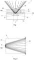
- Figure 1 illustrates a cut section of a portion of a thermal emitter device 1 according to one embodiment of the invention.
- the thermal emitter device 1 comprises a thermal emitting membrane 10 comprising a first surface 11 and a second surface 12, the second surface 12 being opposite to the first surface 11, wherein the thermal emitting membrane 1 is arranged to be heated to a thermal emission temperature so that the first and second surfaces 11, 12 radiate light 100 at the thermal emission temperature.
- the size and the proportion of the different elements illustrated in Figure 1 are just indicative and do not necessarily correspond to the real size respectively proportion.
- the emissivity ⁇ of a surface is lower than 0.7.
- the membrane 10 is monolithic. If the membrane 10 is monolithic, then the second surface 12 will have the same emissivity ⁇ of the first surface 11.
- the first and second surfaces 11, 12 are made by the same material. In another embodiment, the first and second surfaces 11, 12 are made by different materials, but having both an emissivity lower than 0.7.
- Non limitative examples of material having an emissivity lower than 0.7 in the IR and visible spectrum comprises a refractory material, e.g., a refractory metal and their alloys. Examples of refractory metals are Tungsten, Titanium, Hafnium, Zirconium, Tantalum, Molybdenum and their Nitrides, Oxides and Carbides.
- first and second surfaces 11, 12 have been represented as parallel, this is not essential for the invention.
- first and second surfaces 11, 12 have been represented as substantially plate-like, again this is not essential for the invention.
- the invention is particularly adapted for a flat thermal emitting membrane 10.
- the thermal emitting membrane 10 is a single piece membrane. In another embodiment (not illustrated), the thermal emitting membrane 10 is a multi-layer membrane, i.e., it comprises at least one layer (of a different material) between the first and second surfaces 11, 12.
- the thermal emitter device 1 comprises a plurality of resistive arms 4 connected to the thermal emitting membrane 10.
- the resistive arms 4 connect the thermal emitting membrane 10 to a support 13.
- the thermal emitting membrane 10 is suspended by the resistive arms 4, and it is heated to a thermal emission temperature via those resistive arms 4.
- the thermal emitter device 1 comprises also a lens 2.
- the lens 2 comprises a lens entry surface 21, which faces the first surface 11 of the thermal emitting membrane 10 in Figure 1 .
- the lens 2 comprises a lens exit surface 22, opposite to the lens entry surface 21.
- the lens entry surface 21 is substantially flat and the lens exit surface 22 comprises a curved portion 24, in particular a convex portion 24.
- the lens is monobloc and made by the same material. In other embodiments, the lens could comprise two or more pieces and/or could be made of different materials. In one embodiment, a (plano-convex) lens is placed on the lid, e.g. with glue or any other adapted fixation means.
- the thermal emitting membrane 10 is placed in a housing 8 defined by the lens 2 and the support 13.
- this housing 8 comprises vacuum or a controlled atmosphere e.g., without oxygen or other gases which would react with the emitting material at high temperature.
- the lens 2 has a reflectivity normal to a lens surface, e.g., the lens entry surface 21, comprised in the range 4% to 40%, so as to partially reflect the radiated light.
- the lens 2 is made of glass, silicon, sapphire, quartz, germanium, and/or a MID-Far thermal material, such as CaF2, MgF2, ZnSe, ZnS, NaCl.
- a MID-Far thermal material such as CaF2, MgF2, ZnSe, ZnS, NaCl.
- the distance d between the lens entry surface 21 and the first surface 11 of the thermal emitting membrane 10 is equal or lower than L/4, where L is a major dimension of the thermal emitting membrane 10.
- thermal emitting membrane 10 has a rectangular section, its major dimension L is the longer side of the rectangular section. If the thermal emitting membrane 10 has a circular section, its major dimension L is the diameter of the circular section.
- the lens 2 is placed really "close” to the thermal emitter device 10. In this way, a part of the light reflected by the lens 2 is reabsorbed by the thermal emitting membrane 10, and another part of the light reflected by the lens 2 is reflected by the thermal emitting membrane 10 toward the lens 2, having therefore another chance to go through the lens: this allows to increase the efficiency and/or the lifetime of the thermal emitter device.
- the distance d between the lens entry surface 21 and the first surface 11 of the thermal emitting membrane 10 is equal or lower than U8.
- the lens 2 is closer to the thermal emitting membrane 10, thereby increasing more the efficiency and/or the lifetime of the thermal emitter device.
- the thermal emitter device 1 comprises a lid and the lens 2 is placed in or on the lid.
- Using a lens 2 close to the thermal emitting membrane 10 changes the angle dispersion of the thermal emitted light.
- the refraction at the interface between the housing 8 and the lens entry surface 21 allows to convert all angles, so that all light propagates at angles less than a maximum angle related to the angle of total internal reflection at surface 21 due to the material of the lens 2 a.
- the maximum angle is about 40°; if the lens 2 is made of in silicon, the maximum angle is about 16°.
- Figure 2 illustrates a cut view of a lens 2 of a thermal emitter device according to another embodiment of the invention.
- the lens 2 is made by silicon and comprises an entry surface lens 21 and an exit surface lens 22 substantially parallel to the entry surface lens 21, both the entry surface lens 21 and the exit surface lens 22 being substantially flat.
- the thermal emitter device 1 exploits those reflections, by using a thermal emitting membrane 10 which is not a perfect blackbody.
- the thermal emitting membrane 10 has emissivity of lower than 0.7, depending on wavelength and material. This means it has a reflectivity of 30% or higher. According to the invention, the thermal emitting membrane 10 is placed close to the lens: therefore, the light reflected from the lens 2 will hit the first surface 11 of the thermal emitting membrane 10, and either be reabsorbed by the thermal emitting membrane 10 or reflected by the thermal emitting membrane 10 towards the lens, which then has a second chance to go through the lens 2.
- T lens being the transmission of the first surface of the lens 21, then the light transmitted at the first pass is simply T lens .
- R lens being the light reflected by the lens. After reflection R lens from the thermal emitting membrane 10 with reflectivity R emitter then after one round trip and additional R lens R emitter of light will impinge on the lens 2. Therefore, the total light transmitted after first pass and a single round trip is T lens 1 + R lens R emitter and after n round trips it becomes T lens 1 + R lens R emitter + R lens R emitter 2 + ... .
- Table 1 indicates the total light transmitted after a certain number of round trips, for a thermal emitter device having an emissivity equal to 0.4 and a reflectivity R emitter equal to 0.6
- Table 2 indicates the total light transmitted after a certain number of round trips, for a thermal emitter device having an emissivity equal to 0.2 and a reflectivity R emitter equal to 0.8:
- Table 1 No of round trips Transmission 0 68.49% 1 81.43% 2 83.88% 3 84.35% N 84.45%
- Table 2 No of round trips Transmission 0 68.49% 1 85.75% 2 90.10% 3 91.20% N 91.57%
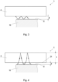
- Figure 3 illustrates a cut view of a thermal emitter device 1 according to another embodiment of the invention.
- a similar advantage can be obtained by exploiting the lens exit surface 22, as long as the lens 2 is "thin".
- the thickness of the lens 2 is such that lens exit surface 22 can also be deemed as being close to lens entrance surface 21 as defined above.
- a lens 2 is "thin” if the lens apparent thickness is less than U4 (or U8). In this embodiment, the distance between the lens entry surface 21 and the surface 11 of the thermal emitting membrane, is less than U4 (or U8).
- Figure 4 illustrates a cut view of a thermal emitter device 1 comprising a "thin" lens 2, according to another embodiment of the invention.
- the refractive index of the lens 2 is taken to be around 3.5 in Figure 4 .
- the thickness is the apparent thickness of the lens when viewed at 45°.
- the refractive index, n is 3.5 then the scale factor is 0.21, so the window appears 0.21 times closer than in reality.
- the scale factor is 0.53.
- the entry and the lens exit surfaces 21, 22 of a "thin" lenses 2 are substantially flat.
- Figure 5 illustrates a cut view of a "thick" lens 2 of a thermal emitter device according to another embodiment of the invention.
- the showed map scale gives just an indication of a possible size of the "thick" lens 2 and should not be considered as limitative.
- the lens exit surface 22 is (at least partially) curved, so as to refocus via reflection at least part of the light back onto the thermal emitting membrane 10. In one embodiment, at least a portion of the lens exit surface 22 is convex. In the embodiment of Figure 5 , all the lenses exit surface 22 is convex.
- lens 2 comprising an exit curved lens exit surface 22. Not only does it enhance the efficiency of the thermal emitter device 1, but it also makes the emission more directional.
- the thermal emitter device 1 comprises an external optics to collimate further the emitted light.
- Figure 6 illustrates a cut view of the "thick" lens 2 of a thermal emitter device 1 of Figure 5 , with an embodiment of the light propagation beyond the lens exit surface.
- the beams are not deviated at the lens exit surface 22.
- the beams could be deviated at the lens exit surface 22.
- the showed map scale gives just an indication of a possible size of the "thick" lens 2 and should not be considered as limitative.
- Figure 7 illustrates a cut view of a "thick" lens 2 of a thermal emitter device, comprising a mirror on a portion 23 of the lens exit surface 22, according to another embodiment of the invention.
- the showed map scale gives just an indication of a possible size of the "thick" lens 2 and should not be considered as limitative.
- the lens exit surface 22 comprised a curved portion 24.
- the mirror 23 is placed at the two ends of the curved portion 24, by restricting therefore the exit angle of the light beam, thereby improving its directionality.
- the thermal emitting membrane 10 (not visible in Figure 7 ) is curved. This allows to increase more the number of trips on the emitted light in the lens 2.
- the mirror portion 23 is slightly defocused, i.e., the emitter is not placed at the exact focal point, the blur should remain small on a scale of the emitter dimension; in another embodiment, the thermal emitting membrane is slightly curved (bowed upwards towards the lens), so that the light reflected from the mirror 23 does not retract exactly the original path. The bowing should be small on the scale of the scale of the emitter dimension.
- the mirrored portion 23 comprises an off-axis aperture on the exit lens surface. This allows to improve the device emissivity.
- the device emissivity is improved by using a using a (cold) mirror.
- Figure 8 illustrates schematically a thermal emitter system 1000 comprising a cold mirror 200, i.e., with a mirror that does not emit at the wavelength of interest.
- the mirror is illustrated as a curved one, the invention is not limited to a curved mirror, but include any shape of mirrors, comprising e.g., flat mirrors.
- the size and the proportion of the different elements of Figure 8 are just indicative and do not necessarily correspond to the actual size respectively proportion. The same applies to the inclination of the depicted arrows.
- This embodiment is based on the reflection by the cold mirror 200 of some of the light emitted from the first thermal emitter device 100 back off the same surface, in order to increase the effective emissivity or the first thermal emitter device 100.
- P 3 R m ⁇ R ⁇ ⁇ ⁇ dA 1 ⁇ ⁇ 1
- R m is the reflectivity of the material of the first thermal emitter device 100.
- the total emission power is conserved, less possible loss in the mirror 200.
- the power towards optic can never exceed dA, ⁇ ⁇ 1 , so that the second law of thermodynamics is satisfied.
- the thermal emitter device according to one embodiment of the invention is an implementation of the idea depicted in Figure 8 .
- Figure 9 illustrates a cut view of a thermal emitter device 1 according to one embodiment of the invention, comprising an off-axis mirror 23.
- the mirror comprises an opening 26.
- the thermal emitter device 1 of Figure 9 comprises also a (not-illustrated) lens, according to the disclosure.
- the emission in a cone ⁇ 1 towards the mirror 23 is reflected back on to the thermal emitting membrane 10.
- Part of the power is reabsorbed in the thermal emitting membrane 10 and part of the power is reflected out through the opening 26, which sums with the original power emitted towards the opening 26, thus enhancing the power out.
- Figure 10 illustrates a cut view of a thermal emitter device 1 according to another embodiment of the invention, comprising an off-axis mirror on the lens exit surface 22.
- the opening 26 is on the lens exit surface 22 22 so the light is more directional.
- This embodiment combines the advantage of a (close) lens (to collect angles) along with the mirror 23 to reflect light off the sample.
- Figure 11 illustrates a cut view of a thermal emitter device 1 according to another embodiment of the invention, comprising an off-axis mirror on the lens exit surface 22.
- the opening could have a different shape to the rest of the lens 2, in order to control the light further.
- FIG 12 shows an example of a thermal emitter device 1 according to the invention, wherein the thermal emitting membrane 10 comprises a plurality of resistive arms 4 connected to the thermal emitting membrane 10, wherein the thermal emitting membrane 10 is suspended by the resistive arms, wherein the thermal emitting membrane 10 is heated to a thermal emission temperature via those resistive arms 4.
- Each of the arms 4 in the illustrated example of Figure 12 has a length 5, a width 6 and a thickness 7, and a cross-sectional area which is much smaller than that of the membrane 10.
- the connection pads 3 are designed to provide mechanical connection to a substrate such that the membrane 10 is only supported relative to the substrate by the arms 4 and pads 3.
- the connection pads 3 provide electrical connection to the arms 4, and thereby to the membrane 10.
- the membrane 10, pads 3 and arms 4 are preferably made of a single contiguous piece of material.
- Other features and other embodiments of this thermal emitter device 1 and/or of this emitting membrane 10 are described in the documents WO2020012042 , WO2021144463 or WO2021144464 filed by the applicant.
- the membrane 10 comprises different holes, as described in the patent application having the application number EP20220155542 filed by the applicant.
Landscapes
- Physics & Mathematics (AREA)
- General Physics & Mathematics (AREA)
- Spectroscopy & Molecular Physics (AREA)
- Optics & Photonics (AREA)
- Engineering & Computer Science (AREA)
- General Engineering & Computer Science (AREA)
- Chemical & Material Sciences (AREA)
- Ceramic Engineering (AREA)
- Toxicology (AREA)
- Health & Medical Sciences (AREA)
- Optical Elements Other Than Lenses (AREA)
- Lenses (AREA)
- Arrangement Of Elements, Cooling, Sealing, Or The Like Of Lighting Devices (AREA)
- Non-Portable Lighting Devices Or Systems Thereof (AREA)
- Led Device Packages (AREA)
- Resistance Heating (AREA)
Claims (15)
- Wärmestrahlungsvorrichtung (1), umfassend:- eine wärmeabstrahlende Membran (10) mit einer Oberfläche (11; 12), wobei die thermisch emittierende Membran (10) so angeordnet ist, dass sie auf eine Wärmeemissionstemperatur erwärmt werden kann, so dass die Oberfläche IR- oder sichtbares Licht abstrahlt,- eine Linse (2), die eine Linsenoberfläche (21) aufweist, wobei die Linsenoberfläche der Oberfläche (11; 12) der wärmeabstrahlenden Membran (10) zugewandt ist, dadurch gekennzeichnet,dass der Emissionsgrad der Oberfläche (11; 12) weniger als 0.7 beträgt,dass die Linsenoberfläche ein Reflexionsvermögen senkrecht zur Linsenoberfläche im Bereich von 4 % bis 40 % aufweist, so dass das abgestrahlte IR- oder sichtbare Licht teilweise reflektiert wird,dass der Abstand (d) zwischen der Linsenoberfläche (21) und der Oberfläche (11; 12) gleich oder kleiner als L/4 ist, wobei L eine Hauptlänge der wärmeabstrahlenden Membran (10) ist, so dass ein Teil des von der Linse (2) reflektierten IR- oder sichtbaren Lichts von der wärmeabstrahlenden Membran (10) reabsorbiert wird und ein anderer Teil des von der Linse (2) reflektierten IR- oder sichtbaren Lichts von der wärmeabstrahlenden Membran (10) in Richtung der Linse (2) reflektiert wird und somit eine weitere Chance hat, durch die Linse zu fallen, wodurch der Wirkungsgrad der Wärmestrahlungsvorrichtung (1) erhöht wird.
- Die Wärmestrahlungsvorrichtung (1) nach Anspruch 1, wobei der Abstand (d) zwischen der Linse (2) und der Oberfläche (11; 12) gleich oder kleiner als L/8 ist.
- Die Wärmestrahlungsvorrichtung (1) nach einem der Ansprüche 1 oder 2, wobei die Linse (2) aus Glas, Silizium, Saphir, Quarz, Germanium und/oder einem MID-Far-Thermomaterial, wie zum Beispiel CaF2, MgF2, ZnSe, ZnS, NaCl.
- Die Wärmestrahlungsvorrichtung (1) nach einem der Ansprüche 1 bis 3, mit einem Deckel, wobei die Linse (2) in oder auf dem Deckel angeordnet ist.
- Die Wärmestrahlungsvorrichtung (1) nach einem der Ansprüche 1 bis 4, wobei die wärmeabstrahlende Membran (10) aus einem feuerfesten Material, z. B. einem feuerfesten Metall und/oder einer Legierung feuerfester Metalle und/oder einer feuerfesten Keramik, hergestellt ist oder diese umfasst.
- Die Wärmestrahlungsvorrichtung (1) nach einem der Ansprüche 1 bis 5, wobei die Linsenscheindicke der Linse (2) gleich oder kleiner als L/4 ist.
- Die Wärmestrahlungsvorrichtung (1) nach einem der Ansprüche 1 bis 5, wobei die Linsenscheindicke der Linse (2) größer als L/4 ist.
- Die Wärmestrahlungsvorrichtung (1) nach Anspruch 7, wobei die Linsenoberfläche eine Linseneingangsoberfläche (21) ist, die Linse (2) eine Linsenausgangsoberfläche (22) umfasst und die Linsenausgangsoberfläche (22) zumindest teilweise gekrümmt ist, um das Licht wieder auf die wärmeabstrahlende Membran (10) zu fokussieren und/oder um die Emission mehr oder weniger gerichtet zu machen.
- Die Wärmestrahlungsvorrichtung (1) nach Anspruch 7 oder 8, aufweisend einen Spiegel (23) auf mindestens einem Teil der Linsenoberfläche (22).
- Die Wärmestrahlungsvorrichtung (1) nach Anspruch 9, wobei der Spiegel (23) ein außermittiger Spiegel ist.
- Die Wärmestrahlungsvorrichtung (1) nach Anspruch 9 oder 10, wobei der Spiegel (23) ein Kaltlichtspiegel (23) ist.
- Die Wärmestrahlungsvorrichtung (1) nach einem der Ansprüche 9 bis 11, wobei der Spiegel (23) eine Öffnung (26) aufweist.
- Die Wärmestrahlungsvorrichtung (1) nach Anspruch 12, wobei ein Teil der Linse (22), der der Öffnung (26) zugewandt ist, eine andere Form hat als die Linse, die der Öffnung nicht zugewandt ist, um das emittierte Licht weiter auszurichten.
- Die Wärmestrahlungsvorrichtung (1) nach einem der Ansprüche 1 bis 13, die eine Vielzahl von Widerstandsarmen umfasst, die mit der wärmeabstrahlenden Membran verbunden sind, wobei die wärmeabstrahlende Membran an den Widerstandsarmen aufgehängt ist, wobei die wärmeabstrahlende Membran über die Widerstandsarme auf eine Wärmeemissionstemperatur erhitzt wird.
- Die Wärmestrahlungsvorrichtung (1) nach einem der Ansprüche 9 bis 14, wobei die Oberfläche eine erste Oberfläche (11) ist, wobei die Vorrichtung eine zweite Oberfläche (12) aufweist, die der ersten Oberfläche (11) gegenüberliegt, wobei die wärmeabstrahlende Membran (10) so angeordnet ist, dass sie auf eine Wärmeemissionstemperatur erwärmt wird, so dass die erste und die zweite Oberfläche IR- oder sichtbares Licht abstrahlen,wobei der Spiegel (23) einer der ersten oder zweiten Oberflächen (11, 12) der wärmeabstrahlenden Membran (10) gegenüberliegt,wobei mindestens ein Teil der wärmeabstrahlenden Membran (10) durchgehende Löcher (40) aufweist,wobei jeder Querschnitt der Löcher (40) in einer Ebene parallel zu einer der ersten oder zweiten Oberflächen der wärmeabstrahlenden Membran eine maximale Abmessung hat, die größer ist als die längste Wellenlänge des vordefinierten Bereichs,wobei die Summe der Flächen der Löcher (40) mindestens 10% der Fläche jeder der ersten oder zweiten Oberflächen (11, 12) der wärmeabstrahlenden Membran (10) beträgt.
Priority Applications (9)
| Application Number | Priority Date | Filing Date | Title |
|---|---|---|---|
| EP22193994.5A EP4333560B1 (de) | 2022-09-05 | 2022-09-05 | Thermische lichtemittierende vorrichtung |
| US19/107,080 US20250354675A1 (en) | 2022-09-05 | 2023-04-05 | Thermal light emitting device with integrated filter |
| PCT/IB2023/053455 WO2024052740A1 (en) | 2022-09-05 | 2023-04-05 | Thermal light emitting device with integrated filter |
| EP23720183.5A EP4585017A1 (de) | 2022-09-05 | 2023-04-05 | Wärmelichtemittierende vorrichtung mit integriertem filter |
| JP2023140717A JP2024036302A (ja) | 2022-09-05 | 2023-08-31 | 熱発光装置 |
| CN202311134897.2A CN117651352A (zh) | 2022-09-05 | 2023-09-04 | 热发光设备 |
| US18/460,813 US20240084997A1 (en) | 2022-09-05 | 2023-09-05 | Thermal light emitting device |
| KR1020230117473A KR20240033683A (ko) | 2022-09-05 | 2023-09-05 | 열 발광 장치 |
| TW113112713A TW202445106A (zh) | 2022-09-05 | 2024-04-03 | 具有積體濾光器之熱發光裝置 |
Applications Claiming Priority (1)
| Application Number | Priority Date | Filing Date | Title |
|---|---|---|---|
| EP22193994.5A EP4333560B1 (de) | 2022-09-05 | 2022-09-05 | Thermische lichtemittierende vorrichtung |
Publications (3)
| Publication Number | Publication Date |
|---|---|
| EP4333560A1 EP4333560A1 (de) | 2024-03-06 |
| EP4333560C0 EP4333560C0 (de) | 2025-01-22 |
| EP4333560B1 true EP4333560B1 (de) | 2025-01-22 |
Family
ID=83692632
Family Applications (2)
| Application Number | Title | Priority Date | Filing Date |
|---|---|---|---|
| EP22193994.5A Active EP4333560B1 (de) | 2022-09-05 | 2022-09-05 | Thermische lichtemittierende vorrichtung |
| EP23720183.5A Pending EP4585017A1 (de) | 2022-09-05 | 2023-04-05 | Wärmelichtemittierende vorrichtung mit integriertem filter |
Family Applications After (1)
| Application Number | Title | Priority Date | Filing Date |
|---|---|---|---|
| EP23720183.5A Pending EP4585017A1 (de) | 2022-09-05 | 2023-04-05 | Wärmelichtemittierende vorrichtung mit integriertem filter |
Country Status (7)
| Country | Link |
|---|---|
| US (2) | US20250354675A1 (de) |
| EP (2) | EP4333560B1 (de) |
| JP (1) | JP2024036302A (de) |
| KR (1) | KR20240033683A (de) |
| CN (1) | CN117651352A (de) |
| TW (1) | TW202445106A (de) |
| WO (1) | WO2024052740A1 (de) |
Family Cites Families (8)
| Publication number | Priority date | Publication date | Assignee | Title |
|---|---|---|---|---|
| EP2447705A1 (de) * | 2009-06-25 | 2012-05-02 | Panasonic Corporation | Infrarotgasdetektor und infrarotgasmessvorrichtung |
| EP3096345B1 (de) * | 2015-05-22 | 2018-07-11 | CSEM Centre Suisse d'Electronique et de Microtechnique SA - Recherche et Développement | Infrarotemitter |
| AT519870B1 (de) | 2017-07-14 | 2018-11-15 | Efkon Gmbh | Verfahren zum Bestimmen der Dämpfung von Strahlung sowie Vorrichtung mit Infrarotsender und -empfänger |
| US10883804B2 (en) | 2017-12-22 | 2021-01-05 | Ams Sensors Uk Limited | Infra-red device |
| DE102018101974B4 (de) * | 2018-01-30 | 2025-05-15 | Infrasolid Gmbh | Infrarotstrahlungsquelle |
| EP3595403A1 (de) * | 2018-07-13 | 2020-01-15 | Matthias Imboden | Hochtemperatur-infrarotstralelement und -verfahren |
| CA3079443A1 (en) | 2020-01-15 | 2021-07-15 | Matthias Imboden | Metrology device, system and method |
| EP3863371A1 (de) | 2020-02-07 | 2021-08-11 | Infineon Technologies AG | Ir-strahler mit glasdeckel |
-
2022
- 2022-09-05 EP EP22193994.5A patent/EP4333560B1/de active Active
-
2023
- 2023-04-05 US US19/107,080 patent/US20250354675A1/en active Pending
- 2023-04-05 EP EP23720183.5A patent/EP4585017A1/de active Pending
- 2023-04-05 WO PCT/IB2023/053455 patent/WO2024052740A1/en not_active Ceased
- 2023-08-31 JP JP2023140717A patent/JP2024036302A/ja active Pending
- 2023-09-04 CN CN202311134897.2A patent/CN117651352A/zh active Pending
- 2023-09-05 US US18/460,813 patent/US20240084997A1/en active Pending
- 2023-09-05 KR KR1020230117473A patent/KR20240033683A/ko active Pending
-
2024
- 2024-04-03 TW TW113112713A patent/TW202445106A/zh unknown
Also Published As
| Publication number | Publication date |
|---|---|
| EP4585017A1 (de) | 2025-07-16 |
| CN117651352A (zh) | 2024-03-05 |
| EP4333560C0 (de) | 2025-01-22 |
| US20250354675A1 (en) | 2025-11-20 |
| US20240084997A1 (en) | 2024-03-14 |
| WO2024052740A1 (en) | 2024-03-14 |
| KR20240033683A (ko) | 2024-03-12 |
| EP4333560A1 (de) | 2024-03-06 |
| TW202445106A (zh) | 2024-11-16 |
| JP2024036302A (ja) | 2024-03-15 |
Similar Documents
| Publication | Publication Date | Title |
|---|---|---|
| KR101158229B1 (ko) | 포물면 태양 반사경과 함께 사용하기 위한 구면 결상 렌즈를 갖는 광발전기 | |
| US10422499B2 (en) | Integrated planar reflective LARP package and method | |
| CN101088031A (zh) | 用于euv光谱区域的热稳定的多层的反射镜 | |
| JPH0968604A (ja) | 固体カタディオプトリックレンズ | |
| US20100025581A1 (en) | Infrared imaging apparatus | |
| US20070029289A1 (en) | System and method for high power laser processing | |
| US6415783B1 (en) | Solar energy receiver assembly | |
| EP2613132B1 (de) | Gegen Wärmestrahlung abgeschirmtes Infrarotspektrometer mit ungekühlter Optik. | |
| JP2010211247A (ja) | 光学波長分散システム | |
| US4554448A (en) | Optical elements | |
| EP4333560B1 (de) | Thermische lichtemittierende vorrichtung | |
| KR102497712B1 (ko) | 다중분광 스텔스 소자 | |
| JP2022100255A (ja) | 日射計 | |
| US5756992A (en) | Blackbody simulating apparatus for calibrating an infrared imaging device | |
| CN111623886B (zh) | 一种空间光电环境模拟系统及红外太阳模拟器 | |
| US5017786A (en) | V2 O3 protection for IR detector arrays against intense thermal radiation | |
| JP7004597B2 (ja) | 放射冷却装置 | |
| US10254169B2 (en) | Optical detector based on an antireflective structured dielectric surface and a metal absorber | |
| US4251288A (en) | Photovoltaic device with specially arranged luminescent collector and cell | |
| RU2607049C9 (ru) | Солнечный оптический телескоп космического базирования (варианты) | |
| WO2018063939A1 (en) | Laser power and energy sensor using anisotropic thermoelectric material | |
| US10215447B2 (en) | Spectrally selective semiconductor dielectric photonic solar thermal absorber | |
| JP2002221449A (ja) | 放射検出装置 | |
| JP2006046926A (ja) | 放射温度測定装置 | |
| JP2012177560A (ja) | 放射温度計 |
Legal Events
| Date | Code | Title | Description |
|---|---|---|---|
| PUAI | Public reference made under article 153(3) epc to a published international application that has entered the european phase |
Free format text: ORIGINAL CODE: 0009012 |
|
| STAA | Information on the status of an ep patent application or granted ep patent |
Free format text: STATUS: THE APPLICATION HAS BEEN PUBLISHED |
|
| AK | Designated contracting states |
Kind code of ref document: A1 Designated state(s): AL AT BE BG CH CY CZ DE DK EE ES FI FR GB GR HR HU IE IS IT LI LT LU LV MC MK MT NL NO PL PT RO RS SE SI SK SM TR |
|
| STAA | Information on the status of an ep patent application or granted ep patent |
Free format text: STATUS: REQUEST FOR EXAMINATION WAS MADE |
|
| 17P | Request for examination filed |
Effective date: 20240521 |
|
| RBV | Designated contracting states (corrected) |
Designated state(s): AL AT BE BG CH CY CZ DE DK EE ES FI FR GB GR HR HU IE IS IT LI LT LU LV MC MK MT NL NO PL PT RO RS SE SI SK SM TR |
|
| GRAP | Despatch of communication of intention to grant a patent |
Free format text: ORIGINAL CODE: EPIDOSNIGR1 |
|
| STAA | Information on the status of an ep patent application or granted ep patent |
Free format text: STATUS: GRANT OF PATENT IS INTENDED |
|
| GRAS | Grant fee paid |
Free format text: ORIGINAL CODE: EPIDOSNIGR3 |
|
| GRAJ | Information related to disapproval of communication of intention to grant by the applicant or resumption of examination proceedings by the epo deleted |
Free format text: ORIGINAL CODE: EPIDOSDIGR1 |
|
| GRAL | Information related to payment of fee for publishing/printing deleted |
Free format text: ORIGINAL CODE: EPIDOSDIGR3 |
|
| STAA | Information on the status of an ep patent application or granted ep patent |
Free format text: STATUS: REQUEST FOR EXAMINATION WAS MADE |
|
| INTG | Intention to grant announced |
Effective date: 20241004 |
|
| GRAP | Despatch of communication of intention to grant a patent |
Free format text: ORIGINAL CODE: EPIDOSNIGR1 |
|
| STAA | Information on the status of an ep patent application or granted ep patent |
Free format text: STATUS: GRANT OF PATENT IS INTENDED |
|
| INTC | Intention to grant announced (deleted) | ||
| RAP3 | Party data changed (applicant data changed or rights of an application transferred) |
Owner name: 4K-MEMS SA |
|
| GRAA | (expected) grant |
Free format text: ORIGINAL CODE: 0009210 |
|
| STAA | Information on the status of an ep patent application or granted ep patent |
Free format text: STATUS: THE PATENT HAS BEEN GRANTED |
|
| INTG | Intention to grant announced |
Effective date: 20241122 |
|
| AK | Designated contracting states |
Kind code of ref document: B1 Designated state(s): AL AT BE BG CH CY CZ DE DK EE ES FI FR GB GR HR HU IE IS IT LI LT LU LV MC MK MT NL NO PL PT RO RS SE SI SK SM TR |
|
| REG | Reference to a national code |
Ref country code: GB Ref legal event code: FG4D |
|
| REG | Reference to a national code |
Ref country code: CH Ref legal event code: EP |
|
| REG | Reference to a national code |
Ref country code: IE Ref legal event code: FG4D |
|
| REG | Reference to a national code |
Ref country code: DE Ref legal event code: R096 Ref document number: 602022009758 Country of ref document: DE |
|
| U01 | Request for unitary effect filed |
Effective date: 20250127 |
|
| U07 | Unitary effect registered |
Designated state(s): AT BE BG DE DK EE FI FR IT LT LU LV MT NL PT RO SE SI Effective date: 20250131 |
|
| PG25 | Lapsed in a contracting state [announced via postgrant information from national office to epo] |
Ref country code: RS Free format text: LAPSE BECAUSE OF FAILURE TO SUBMIT A TRANSLATION OF THE DESCRIPTION OR TO PAY THE FEE WITHIN THE PRESCRIBED TIME-LIMIT Effective date: 20250422 |
|
| PG25 | Lapsed in a contracting state [announced via postgrant information from national office to epo] |
Ref country code: PL Free format text: LAPSE BECAUSE OF FAILURE TO SUBMIT A TRANSLATION OF THE DESCRIPTION OR TO PAY THE FEE WITHIN THE PRESCRIBED TIME-LIMIT Effective date: 20250122 |
|
| PG25 | Lapsed in a contracting state [announced via postgrant information from national office to epo] |
Ref country code: ES Free format text: LAPSE BECAUSE OF FAILURE TO SUBMIT A TRANSLATION OF THE DESCRIPTION OR TO PAY THE FEE WITHIN THE PRESCRIBED TIME-LIMIT Effective date: 20250122 |
|
| PG25 | Lapsed in a contracting state [announced via postgrant information from national office to epo] |
Ref country code: IS Free format text: LAPSE BECAUSE OF FAILURE TO SUBMIT A TRANSLATION OF THE DESCRIPTION OR TO PAY THE FEE WITHIN THE PRESCRIBED TIME-LIMIT Effective date: 20250522 Ref country code: NO Free format text: LAPSE BECAUSE OF FAILURE TO SUBMIT A TRANSLATION OF THE DESCRIPTION OR TO PAY THE FEE WITHIN THE PRESCRIBED TIME-LIMIT Effective date: 20250422 |
|
| PG25 | Lapsed in a contracting state [announced via postgrant information from national office to epo] |
Ref country code: HR Free format text: LAPSE BECAUSE OF FAILURE TO SUBMIT A TRANSLATION OF THE DESCRIPTION OR TO PAY THE FEE WITHIN THE PRESCRIBED TIME-LIMIT Effective date: 20250122 |
|
| PG25 | Lapsed in a contracting state [announced via postgrant information from national office to epo] |
Ref country code: GR Free format text: LAPSE BECAUSE OF FAILURE TO SUBMIT A TRANSLATION OF THE DESCRIPTION OR TO PAY THE FEE WITHIN THE PRESCRIBED TIME-LIMIT Effective date: 20250423 |
|
| PG25 | Lapsed in a contracting state [announced via postgrant information from national office to epo] |
Ref country code: SM Free format text: LAPSE BECAUSE OF FAILURE TO SUBMIT A TRANSLATION OF THE DESCRIPTION OR TO PAY THE FEE WITHIN THE PRESCRIBED TIME-LIMIT Effective date: 20250122 |
|
| PG25 | Lapsed in a contracting state [announced via postgrant information from national office to epo] |
Ref country code: CZ Free format text: LAPSE BECAUSE OF FAILURE TO SUBMIT A TRANSLATION OF THE DESCRIPTION OR TO PAY THE FEE WITHIN THE PRESCRIBED TIME-LIMIT Effective date: 20250122 |
|
| PG25 | Lapsed in a contracting state [announced via postgrant information from national office to epo] |
Ref country code: SK Free format text: LAPSE BECAUSE OF FAILURE TO SUBMIT A TRANSLATION OF THE DESCRIPTION OR TO PAY THE FEE WITHIN THE PRESCRIBED TIME-LIMIT Effective date: 20250122 |
|
| U20 | Renewal fee for the european patent with unitary effect paid |
Year of fee payment: 4 Effective date: 20250924 |
|
| PLBE | No opposition filed within time limit |
Free format text: ORIGINAL CODE: 0009261 |
|
| STAA | Information on the status of an ep patent application or granted ep patent |
Free format text: STATUS: NO OPPOSITION FILED WITHIN TIME LIMIT |
|
| 26N | No opposition filed |
Effective date: 20251023 |