EP4333044A1 - Substrate, package, electronic component, and light emitting device - Google Patents
Substrate, package, electronic component, and light emitting device Download PDFInfo
- Publication number
- EP4333044A1 EP4333044A1 EP22795644.8A EP22795644A EP4333044A1 EP 4333044 A1 EP4333044 A1 EP 4333044A1 EP 22795644 A EP22795644 A EP 22795644A EP 4333044 A1 EP4333044 A1 EP 4333044A1
- Authority
- EP
- European Patent Office
- Prior art keywords
- substrate
- via conductors
- view
- light emitting
- package
- Prior art date
- Legal status (The legal status is an assumption and is not a legal conclusion. Google has not performed a legal analysis and makes no representation as to the accuracy of the status listed.)
- Pending
Links
Images






Classifications
-
- H—ELECTRICITY
- H10—SEMICONDUCTOR DEVICES; ELECTRIC SOLID-STATE DEVICES NOT OTHERWISE PROVIDED FOR
- H10H—INORGANIC LIGHT-EMITTING SEMICONDUCTOR DEVICES HAVING POTENTIAL BARRIERS
- H10H20/00—Individual inorganic light-emitting semiconductor devices having potential barriers, e.g. light-emitting diodes [LED]
- H10H20/80—Constructional details
- H10H20/85—Packages
- H10H20/858—Means for heat extraction or cooling
- H10H20/8585—Means for heat extraction or cooling being an interconnection
-
- H—ELECTRICITY
- H10—SEMICONDUCTOR DEVICES; ELECTRIC SOLID-STATE DEVICES NOT OTHERWISE PROVIDED FOR
- H10W—GENERIC PACKAGES, INTERCONNECTIONS, CONNECTORS OR OTHER CONSTRUCTIONAL DETAILS OF DEVICES COVERED BY CLASS H10
- H10W70/00—Package substrates; Interposers; Redistribution layers [RDL]
- H10W70/60—Insulating or insulated package substrates; Interposers; Redistribution layers
-
- H—ELECTRICITY
- H05—ELECTRIC TECHNIQUES NOT OTHERWISE PROVIDED FOR
- H05K—PRINTED CIRCUITS; CASINGS OR CONSTRUCTIONAL DETAILS OF ELECTRIC APPARATUS; MANUFACTURE OF ASSEMBLAGES OF ELECTRICAL COMPONENTS
- H05K1/00—Printed circuits
- H05K1/02—Details
- H05K1/11—Printed elements for providing electric connections to or between printed circuits
- H05K1/111—Pads for surface mounting, e.g. lay-out
- H05K1/112—Pads for surface mounting, e.g. lay-out directly combined with via connections
- H05K1/113—Via provided in pad; Pad over filled via
-
- H—ELECTRICITY
- H05—ELECTRIC TECHNIQUES NOT OTHERWISE PROVIDED FOR
- H05K—PRINTED CIRCUITS; CASINGS OR CONSTRUCTIONAL DETAILS OF ELECTRIC APPARATUS; MANUFACTURE OF ASSEMBLAGES OF ELECTRICAL COMPONENTS
- H05K3/00—Apparatus or processes for manufacturing printed circuits
- H05K3/40—Forming printed elements for providing electric connections to or between printed circuits
- H05K3/403—Edge contacts; Windows or holes in the substrate having plural connections on the walls thereof
-
- H—ELECTRICITY
- H10—SEMICONDUCTOR DEVICES; ELECTRIC SOLID-STATE DEVICES NOT OTHERWISE PROVIDED FOR
- H10H—INORGANIC LIGHT-EMITTING SEMICONDUCTOR DEVICES HAVING POTENTIAL BARRIERS
- H10H20/00—Individual inorganic light-emitting semiconductor devices having potential barriers, e.g. light-emitting diodes [LED]
- H10H20/80—Constructional details
- H10H20/81—Bodies
- H10H20/819—Bodies characterised by their shape, e.g. curved or truncated substrates
-
- H—ELECTRICITY
- H10—SEMICONDUCTOR DEVICES; ELECTRIC SOLID-STATE DEVICES NOT OTHERWISE PROVIDED FOR
- H10H—INORGANIC LIGHT-EMITTING SEMICONDUCTOR DEVICES HAVING POTENTIAL BARRIERS
- H10H20/00—Individual inorganic light-emitting semiconductor devices having potential barriers, e.g. light-emitting diodes [LED]
- H10H20/80—Constructional details
- H10H20/85—Packages
- H10H20/857—Interconnections, e.g. lead-frames, bond wires or solder balls
-
- H—ELECTRICITY
- H10—SEMICONDUCTOR DEVICES; ELECTRIC SOLID-STATE DEVICES NOT OTHERWISE PROVIDED FOR
- H10W—GENERIC PACKAGES, INTERCONNECTIONS, CONNECTORS OR OTHER CONSTRUCTIONAL DETAILS OF DEVICES COVERED BY CLASS H10
- H10W90/00—Package configurations
-
- H—ELECTRICITY
- H01—ELECTRIC ELEMENTS
- H01S—DEVICES USING THE PROCESS OF LIGHT AMPLIFICATION BY STIMULATED EMISSION OF RADIATION [LASER] TO AMPLIFY OR GENERATE LIGHT; DEVICES USING STIMULATED EMISSION OF ELECTROMAGNETIC RADIATION IN WAVE RANGES OTHER THAN OPTICAL
- H01S5/00—Semiconductor lasers
- H01S5/02—Structural details or components not essential to laser action
- H01S5/022—Mountings; Housings
- H01S5/02218—Material of the housings; Filling of the housings
- H01S5/0222—Gas-filled housings
-
- H—ELECTRICITY
- H01—ELECTRIC ELEMENTS
- H01S—DEVICES USING THE PROCESS OF LIGHT AMPLIFICATION BY STIMULATED EMISSION OF RADIATION [LASER] TO AMPLIFY OR GENERATE LIGHT; DEVICES USING STIMULATED EMISSION OF ELECTROMAGNETIC RADIATION IN WAVE RANGES OTHER THAN OPTICAL
- H01S5/00—Semiconductor lasers
- H01S5/02—Structural details or components not essential to laser action
- H01S5/022—Mountings; Housings
- H01S5/0225—Out-coupling of light
- H01S5/02257—Out-coupling of light using windows, e.g. specially adapted for back-reflecting light to a detector inside the housing
-
- H—ELECTRICITY
- H01—ELECTRIC ELEMENTS
- H01S—DEVICES USING THE PROCESS OF LIGHT AMPLIFICATION BY STIMULATED EMISSION OF RADIATION [LASER] TO AMPLIFY OR GENERATE LIGHT; DEVICES USING STIMULATED EMISSION OF ELECTROMAGNETIC RADIATION IN WAVE RANGES OTHER THAN OPTICAL
- H01S5/00—Semiconductor lasers
- H01S5/02—Structural details or components not essential to laser action
- H01S5/022—Mountings; Housings
- H01S5/023—Mount members, e.g. sub-mount members
- H01S5/02315—Support members, e.g. bases or carriers
-
- H—ELECTRICITY
- H05—ELECTRIC TECHNIQUES NOT OTHERWISE PROVIDED FOR
- H05K—PRINTED CIRCUITS; CASINGS OR CONSTRUCTIONAL DETAILS OF ELECTRIC APPARATUS; MANUFACTURE OF ASSEMBLAGES OF ELECTRICAL COMPONENTS
- H05K1/00—Printed circuits
- H05K1/02—Details
- H05K1/03—Use of materials for the substrate
- H05K1/0306—Inorganic insulating substrates, e.g. ceramic, glass
-
- H—ELECTRICITY
- H05—ELECTRIC TECHNIQUES NOT OTHERWISE PROVIDED FOR
- H05K—PRINTED CIRCUITS; CASINGS OR CONSTRUCTIONAL DETAILS OF ELECTRIC APPARATUS; MANUFACTURE OF ASSEMBLAGES OF ELECTRICAL COMPONENTS
- H05K1/00—Printed circuits
- H05K1/02—Details
- H05K1/14—Structural association of two or more printed circuits
- H05K1/141—One or more single auxiliary printed circuits mounted on a main printed circuit, e.g. modules, adapters
-
- H—ELECTRICITY
- H05—ELECTRIC TECHNIQUES NOT OTHERWISE PROVIDED FOR
- H05K—PRINTED CIRCUITS; CASINGS OR CONSTRUCTIONAL DETAILS OF ELECTRIC APPARATUS; MANUFACTURE OF ASSEMBLAGES OF ELECTRICAL COMPONENTS
- H05K2201/00—Indexing scheme relating to printed circuits covered by H05K1/00
- H05K2201/09—Shape and layout
- H05K2201/09145—Edge details
- H05K2201/09181—Notches in edge pads
-
- H—ELECTRICITY
- H05—ELECTRIC TECHNIQUES NOT OTHERWISE PROVIDED FOR
- H05K—PRINTED CIRCUITS; CASINGS OR CONSTRUCTIONAL DETAILS OF ELECTRIC APPARATUS; MANUFACTURE OF ASSEMBLAGES OF ELECTRICAL COMPONENTS
- H05K2201/00—Indexing scheme relating to printed circuits covered by H05K1/00
- H05K2201/09—Shape and layout
- H05K2201/09818—Shape or layout details not covered by a single group of H05K2201/09009 - H05K2201/09809
- H05K2201/09845—Stepped hole, via, edge, bump or conductor
-
- H—ELECTRICITY
- H05—ELECTRIC TECHNIQUES NOT OTHERWISE PROVIDED FOR
- H05K—PRINTED CIRCUITS; CASINGS OR CONSTRUCTIONAL DETAILS OF ELECTRIC APPARATUS; MANUFACTURE OF ASSEMBLAGES OF ELECTRICAL COMPONENTS
- H05K2201/00—Indexing scheme relating to printed circuits covered by H05K1/00
- H05K2201/10—Details of components or other objects attached to or integrated in a printed circuit board
- H05K2201/10007—Types of components
- H05K2201/10106—Light emitting diode [LED]
-
- H—ELECTRICITY
- H10—SEMICONDUCTOR DEVICES; ELECTRIC SOLID-STATE DEVICES NOT OTHERWISE PROVIDED FOR
- H10H—INORGANIC LIGHT-EMITTING SEMICONDUCTOR DEVICES HAVING POTENTIAL BARRIERS
- H10H20/00—Individual inorganic light-emitting semiconductor devices having potential barriers, e.g. light-emitting diodes [LED]
- H10H20/80—Constructional details
- H10H20/85—Packages
- H10H20/8506—Containers
Definitions
- the present disclosure relates to a substrate, a package, an electronic component, and a light emitting device.
- a light emitting module described in Patent Document 1 includes a carrier (substrate) on which a semiconductor laser mounted on a submount (protruding portion) and a lens component are mounted.
- Patent Document 1 JP 2013-80900 A
- a substrate in an aspect of the present disclosure, includes a first substrate having a first surface on which an element is to be mounted, a second surface opposite the first surface, and a first side surface connecting the first surface and the second surface, a second substrate larger than the first substrate and having a third surface supporting the first substrate and a fourth surface opposite the third surface, and first via conductors configured to electrically connect the first surface and the second surface and exposed on the first side surface of the first substrate from the first surface to the second surface.
- a package includes the substrate and a lid.
- an electronic component includes the substrate or the package, and an element mounted in the package.
- a light emitting device includes the substrate or the package, and an element mounted in the package, in which the element is a light emitting element.
- FIG. 1 is a perspective view of a substrate 1 according to the present embodiment.
- FIG. 2 includes a top view, a cross-sectional view, side views, and a bottom view of the substrate 1.
- a view indicated by reference numeral 201 is the top view of the substrate 1
- a view indicated by reference numeral 202 is the cross-sectional view taken along line I-I in the view indicated by reference numeral 201.
- a view indicated by reference numeral 203 is a side view of the substrate 1 when viewed from a negative direction of an X-axis
- a view indicated by reference numeral 204 is a side view of the substrate 1 when viewed from a positive direction of a Y-axis.
- a view indicated by reference numeral 205 in FIG. 2 is the bottom view of the substrate 1.
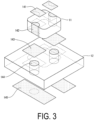
- FIG. 3 is an exploded perspective view of the substrate 1.
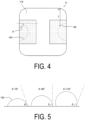
- FIG. 4 is a top view of a first substrate 11 included in the substrate 1.
- the substrate 1 is assumed to be located on an X-Y plane in a virtual XYZ space.
- an upward direction refers to a positive direction of a virtual Z-axis.
- the terms "up/top” and “down/bottom” are used in the following description by way of convenience and are not to be construed as limiting in the actual use of the substrate 1 or the like.
- a thickness direction of the substrate 1 refers to the direction of the Z-axis.
- the substrate 1 is a substrate for mounting an element and functions as a support for supporting the element.
- the substrate 1 can be used for mounting an element that requires heat dissipation and/or an element that requires reduction in conductor resistance. More specifically, the substrate 1 can be used for mounting, for example, an element such as a light emitting element such as a light emitting diode (LED) or a laser diode (LD), a light receiving element such as a photo diode (PD), a charge coupled device (CCD) type or a complementary metal oxide semiconductor (CMOS) type imaging element, or a sensor element such as an acceleration sensor.
- a light emitting element such as a light emitting diode (LED) or a laser diode (LD)
- a light receiving element such as a photo diode (PD), a charge coupled device (CCD) type or a complementary metal oxide semiconductor (CMOS) type imaging element
- a sensor element such as an acceleration sensor.
- the substrate 1 includes the first substrate 11 and a second substrate 12 that supports the first substrate 11 and is larger than the first substrate 11. Specifically, when viewed in plan from the Z-axis direction, the second substrate 12 is larger than the first substrate 11. Therefore, part of a third surface 12A (upper surface) of the second substrate 12 is covered with the first substrate 11, and at least part of a surrounding area is not covered.
- the first substrate 11 has, for example, a rectangular shape, and has a first surface 11A having a region on which an element is to be mounted (hereinafter referred to as an element mounting region 13) and a second surface 11B located opposite the first surface 11A.
- the second substrate 12 has the third surface 12A supporting the first substrate 11 and a fourth surface 12B located opposite the third surface 12A.
- the first substrate 11 and the second substrate 12 have, for example, a rectangular shape.
- the shape of the first substrate 11 and the second substrate 12 is not limited to rectangular, and may be circular or polygonal.
- the element mounting region 13 is a region on which an element is to be mounted on the first surface 11A, and is a region indicated by dashed lines in each of the accompanying drawings.
- a shape of the element mounting region 13 is square, but is not limited thereto, and may be a shape corresponding to a shape of an element to be mounted.
- a ceramic such as an aluminum oxide sintered body (alumina ceramic), an aluminum nitride sintered body, a silicon nitride sintered body, a mullite sintered body, or a glass ceramic sintered body can be used.
- a slurry is prepared by adding and mixing a suitable organic binder, solvent, and the like with raw material powders such as aluminum oxide (Al 2 O 3 ), silicon oxide (SiO 2 ), magnesium oxide (MgO), and calcium oxide (CaO).
- a ceramic green sheet is produced by forming this slurry into a sheet by employing a well-known doctor blade method, calender roll method, or the like. Subsequently, this ceramic green sheet is subjected to an appropriate punching process, and multiple ceramic green sheets are stacked to form a green body, which is then fired at a high temperature (approximately 1600°C) to produce the first substrate 11 and the second substrate 12.
- Wiring conductors 14 are provided on the surface and inside of the substrate 1.
- the substrate 1 includes connection pads 141, first via conductors 142, wiring layers 143, second via conductors 144, and terminal electrodes 145 as the wiring conductors 14.
- connection pads 141 for connection with an element are provided on an upper surface of the substrate 1 (first surface 11A).
- the terminal electrodes 145 for connection with an external electrical circuit are provided on a lower surface of the substrate 1 (fourth surface 12B).
- the terminal electrodes 145 are not limited to being provided on the lower surface of the substrate 1, and may be provided on side surfaces from the lower surface or on the side surfaces of the substrate 1.
- These connection pads 141 and the terminal electrodes 145 are electrically connected by the first via conductors 142, the wiring layers 143, and the second via conductors 144 provided on the surface and inside of the substrate 1.
- connection pads 141 and the terminal electrodes 145 mainly contain, for example, metals such as tungsten, molybdenum, manganese, copper, silver, palladium, gold, platinum, nickel, or cobalt, or alloys containing any of these metals as conductor materials.
- the connection pads 141 and the terminal electrodes 145 are formed on the surfaces of the substrate 1 as metal layers such as metallization layers or plating layers of a conductor material.
- the wiring layers 143 are formed inside the substrate 1 by metallization of a conductor material.
- the first substrate 11 and the second substrate 12 are different in size. Thus, the wiring layers 143 placed between the first substrate 11 and the second substrate 12 may be exposed on the surface of the second substrate 12.
- connection pads 141, the wiring layers 143, and the terminal electrodes 145 are, for example, metallization layers of tungsten
- they can be formed by printing a metal paste prepared by mixing tungsten powder with an organic solvent and an organic binder at predetermined positions on the ceramic green sheets to be the substrate 1 by a screen printing method or the like and firing the paste.
- a plating layer of nickel, gold, or the like may be further deposited on exposed surfaces of the metallization layers to serve as the connection pads 141, the wiring layers 143, and the terminal electrodes 145 by using an electrolytic plating method, electroless plating method, or the like.
- the first via conductors 142 are via conductors that electrically connect the first surface 11A side and the second surface 11B side and are exposed on the side surfaces of first substrate 11 from the first surface 11A to the second surface 11B.
- the first via conductors 142 electrically connect conductors on the first surface 11A and conductors on the second surface 11B.
- the first via conductors 142 electrically connect the connection pads 141 on the first surface 11A and the wiring conductors (wiring layers 143) on the second surface.
- the second via conductors 144 are via conductors that electrically connect the third surface 12A side and the fourth surface 12B side.
- the second via conductors 144 electrically connect conductors on the third surface 12A and conductors on the fourth surface 12B.
- the second via conductors 144 electrically connect the wiring layers 143 on the third surface 12A and the terminal electrodes 145 on the fourth surface 12B.
- via conductors may be used as a generic term for the first via conductors 142 and the second via conductors 144. That is, the via conductors are conductors passing through the first substrate 11 or the second substrate 12.
- the via conductors may be formed at predetermined positions in the ceramic green sheet prior to printing of the metal paste for forming the connection pads 141, the wiring layers 143, and the terminal electrodes 145. For example, first, through holes for via conductors are formed in the ceramic green sheet for the first substrate 11 or the second substrate 12 by a machining method such as stamping using a die or punching or laser beam machining.
- the through holes are filled with a metallization paste for via conductors by the above printing method, and the via conductors are formed by firing together with the ceramic green sheet for the first substrate 11 or the second substrate 12.
- the metallization paste is prepared by kneading the metal powder described above with an appropriate solvent and binder to adjust viscosity to an appropriate level.
- the metallization paste may contain glass powder or ceramic powder in order to increase bonding strength with the first substrate 11 or the second substrate 12.
- the via conductors other than the first via conductors 142 have, for example, a circular shape when viewed in plan from the Z-axis direction. That is, for example, in the first substrate 11 of the present embodiment, the second via conductors 144 are cylindrical. However, the shape of the via conductors is not limited to cylindrical, and may be oval, polygonal, or prismatic, for example.
- all of the via conductors included in the first substrate 11 are the first via conductors 142, but the first substrate 11 may include via conductors that are not exposed on the side surfaces of the first substrate 11.
- the first via conductors 142 have, for example, a semi-circular shape when viewed in plan from the Z-axis direction. That is, the first via conductors 142 may be, for example, semi-cylindrical.
- the shape of the first via conductors 142 when viewed in plan is not limited to semi-circular, and may be semi-elliptical or rectangular.
- the shape of the first via conductors 142 as viewed in plan is a shape without corners such as a semi-circular shape or a semi-elliptical shape, the likelihood of cracks in the first substrate 11 originating from the corners can be reduced.
- the sizes of the multiple first via conductors 142 included in the first substrate 11 may be different from each other.
- the first via conductors 142 may be formed as follows, for example. That is, (i) in the ceramic green sheet to be the first substrate 11, forming via conductors based on positions of the first via conductors 142 in the first substrate 11. (ii) Punching out the first substrate 11 such that at least part of the via conductors is exposed on the side surfaces of the first substrate 11 using a die corresponding to the shape of the first substrate 11.
- the first via conductors 142 having a semi-cylindrical shape can be formed by forming cylindrical via conductors in (i) and punching out in (ii).
- the exposed surfaces of the first via conductors 142 may be further coated with a plating layer of nickel, gold, or the like using an electrolytic plating method, an electroless plating method, or the like.
- the step (ii) may be performed after the ceramic green sheet to be the second substrate 12 is positioned below the ceramic green sheet to be the first substrate 11, with the first substrate 11 and the second substrate 12 aligned, so that they have a predetermined positional relationship.
- an appropriate binder obtained by adding and mixing a resin, a solvent, and the like may be applied to a portion to be the second surface 11B of the first substrate 11, and a portion to be the first substrate 11 may be pressed against the portion to be the third surface 12A of the second substrate 12 for adhesion while punching out the portion to be the first substrate 11.
- the punching process of the portion to be the first substrate 11 and the stacking step of the portion to be the first substrate 11 and the portion to be the second substrate 12 may be performed simultaneously.
- positional accuracy when mounting the first substrate 11 on the second substrate 12 may be improved.
- connection pads 141 connected to the element and the terminal electrodes 145 are connected by the via conductors having wider cross-sectional areas than connection wires or the like, thereby achieving low conductor resistance.
- the via conductors included in the first substrate 11 close to the element are exposed on the side surfaces of the first substrate 11, which provide excellent heat dissipation.
- the first substrate 11 is smaller than the second substrate 12, an area occupied by the wiring conductors 14 is relatively large with respect to an area of the first substrate 11 in a horizontal cross section of the first substrate 11 when viewed in plan. Therefore, when the via conductors are formed inside the first substrate, distances between the via conductors and the side surfaces of the first substrate 11 may be insufficient depending on the positions of the via conductors. Cracks may occur in the first substrate 11 at locations where the distance between the outer edge of the via conductor and the side surface of the first substrate 11 is not sufficient. However, the first via conductors 142 of the present embodiment are exposed from the first surface 11A to the second surface 11B, which reduces a possibility of such cracks. Even when other through-hole conductors need to be provided in order to mount a semiconductor element, a capacitor, or the like other than the element described above on the first substrate, wiring layout flexibility can be improved while reducing the possibility of cracks.
- the first via conductors 142 have portions overlapping the second via conductors 144 when viewed in plan.
- heat and current conduction paths are formed in straight lines and with large cross-sectional areas from the first surface 11A on which the element is mounted to the fourth surface 12B connected to the mounting substrate, further improving heat dissipation and an effect of reducing conductor resistance.
- the cross-sectional area of the second via conductors 144 is larger than the cross-sectional area of the first via conductors 142.
- heat transfer paths from the first surface 11A to the fourth surface 12B also extend in the X-Y plane direction, so heat is transferred to the fourth surface 12B while diffusing in the X-Y plane direction.
- heat dissipation can be further improved.
- FIG. 4 is a top view of the first substrate 11.
- FIG. 5 is a schematic plan view schematically illustrating an outer edge of the first via conductor 142 and a side of the first surface 11A when an angle ⁇ illustrated in FIG. 4 is changed.
- the first substrate 11 may include the first via conductors 142 at the centers of opposite sides of the first surface 11A.
- This configuration increases a distance L between the first via conductor 142 and a side at which the first via conductor 142 is not located, thereby reducing a possibility of cracks in the first substrate 11 due to stress such as thermal stress caused by heat generated during use.
- the distance L can be defined as the shortest distance from the side where the first via conductor 142 is not located to a position where an extension line orthogonal to the side intersects the outer edge of the first via conductor 142.
- An angle between a tangent to the outer edge of the first via conductor 142 at the intersection and the side of the first surface 11A is defined as an angle ⁇ .
- the angle ⁇ may be from 70° to 110° (90° ⁇ 20°).
- FIG. 6 includes a top view, a cross-sectional view, side views, and a bottom view of a substrate 1P that is a variation of the substrate 1.
- a view indicated by reference numeral 601 is the top view of the substrate 1P
- a view indicated by reference numeral 602 is the cross-sectional view taken along line II-II in the view indicated by reference numeral 601.
- a view indicated by reference numeral 603 is a side view of the substrate 1P when viewed from the negative direction of the X-axis
- a view indicated by reference numeral 604 is a side view of the substrate 1P when viewed from the positive direction of the Y-axis.
- a view indicated by reference numeral 605 in FIG. 6 is the bottom view of the substrate 1P.
- a first substrate 11P according to a first variation includes first via conductors 142P.
- a cross-sectional area of the first via conductors 142P in a cross section parallel to the first surface 11A increases from the first surface 11A toward the second surface 11B.
- the cross-sectional area may increase stepwise from the first surface 11A toward the second surface 11B, or may gradually increase from the first surface 11A toward the second surface 11B.
- the above configuration of the first via conductors 142P improves heat dissipation because heat from the element is transferred to the second substrate side while diffusing in a plane direction as well. Connection areas between the first via conductors 142P and the wiring layers 143 on a second substrate 12P are increased, thereby improving connection reliability. The large conduction cross-sectional area further reduces the conductor resistance compared with the first via conductors 142.
- the second substrate 12P of the substrate 1P includes second via conductors 144P.
- the cross-sectional area of the second via conductors 144P in a cross section parallel to the third surface 12A increases from the third surface toward the fourth surface.
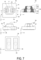
- FIG. 7 includes a top view, a cross-sectional view, side views, and a bottom view of a substrate 1Q that is a variation of the substrate 1.
- a view indicated by reference numeral 701 is the top view of the substrate 1Q
- a view indicated by reference numeral 702 is a cross-sectional view taken along line III-III in the view indicated by reference numeral 701.
- a view indicated by reference numeral 703 is a side view of the substrate 1Q when viewed from the positive direction of the X-axis
- a view indicated by reference numeral 704 is a side view of the substrate 1Q when viewed from the positive direction of the Y-axis.
- a view indicated by reference numeral 705 in FIG. 7 is the bottom view of the substrate 1Q.
- Second variation Side surfaces of a first substrate 11Q according to a second variation are inclined, and an angle ⁇ P between the side surfaces and the third surface 12A is an obtuse angle.
- Surfaces of the first via conductors 142Q exposed on the side surfaces of the first substrate 11Q may be flush with the side surfaces of the first substrate 11Q, and the exposed surfaces of the first via conductors 142Q may also be inclined.
- the angle between the exposed surfaces and the third surface 12A may be the same as the angle ⁇ P between the side surfaces and the third surface 12A.
- the angle ⁇ P is not limited, and may be, for example, from 95° to 110°.
- the inclined surfaces of the first substrate 11Q can be formed, for example, by providing a clearance between dies in the step of punching out the ceramic green sheet to be the first substrate 11Q.
- the inclined surfaces can be formed by setting a diameter (length of one side) of a support die (female die) installed on a punching end surface side of the first substrate 11Q to be larger than a diameter (length of one side) of a punching die (male die) installed on a punching start surface side of the first substrate 11Q.
- the inclination angle (angle ⁇ P) of the first substrate 11Q can be adjusted by changing the size of the clearance between the male die and the female die.
- the angle ⁇ P between the side surfaces of the first substrate 11Q and the third surface 12A is an obtuse angle, which reduces a possibility of cracks originating from the corners. This reduces the likelihood of disconnection of the wiring, thereby improving reliability.
- the substrate 1Q in which the angle ⁇ P is an obtuse angle has excellent heat dissipation because areas of the first via conductors 142Q exposed to the side surfaces of the first substrate 11Q are larger than that of the substrate in which the angle ⁇ P is a right angle.
- the first via conductors 142Q further increase a conductor cross-sectional area and increase thermal diffusion in a lateral direction, which further improves a conductor resistance reduction effect and a heat dissipation effect.
- FIG. 8 includes a top view, a cross-sectional view, side views, and a bottom view of a substrate 1R that is a variation of the substrate 1.
- a view indicated by reference numeral 801 is the top view of the substrate 1R
- a view indicated by reference numeral 802 is a cross-sectional view taken along line IV-IV in the view indicated by reference numeral 801.
- a view indicated by reference numeral 803 is a side view of the substrate 1R when viewed from the negative direction of the X-axis
- a view indicated by reference numeral 804 is a side view of the substrate 1R when viewed from the positive direction of the Y-axis.
- a view indicated by reference numeral 805 in FIG. 8 is the bottom view of the substrate 1R.
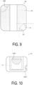
- FIG. 9 is an enlarged top view of a first substrate 11R.
- the substrate 1R according to a third variation has a rectangular shape, and includes first via conductors 142R at opposite corners of the first surface 11A.
- the distance between outer edges of the first via conductors 142R can be increased, thereby reducing the likelihood of cracks occurring in a portion between the first via conductors 142R of the first substrate 11R.
- Diameters of the first via conductors 142R can be increased, which further improves a conductor resistance reduction effect and a heat dissipation effect.
- angles ⁇ 1 and ⁇ 2 may be different from each other.
- the angles ⁇ 1 and ⁇ 2 may each be from 70° to 110° (90° ⁇ 20°).
- FIG. 10 is a top view of a first substrate 11S that is a variation of the first substrate 11.
- the first substrate 11S includes two first via conductors 142S1 and 142S2 of different sizes.
- the first via conductor 142S1 has a semi-elliptical shape, and part of the first via conductor 142S1 overlaps the element mounting region 13 when viewed in plan.
- the region overlapping the element mounting region 13 when viewed in plan is larger than that in the embodiment and variations described above. Consequently, heat dissipation can be further improved.
- the first via conductor 142S1 having a larger cross-sectional area may be used as ground potential, and the first via conductor 142S2 having a smaller cross-sectional area may be used as potential for power extraction.
- the first via conductor 142S1 may be connected to a wiring conductor through, for example, an electrically conductive bonding material (solder, brazing material, electrically conductive adhesive, etc.) placed on a lower surface of the first substrate 11S.
- first via conductor 142S2 may be connected to a wiring conductor through a bonding wire.
- one first via conductor 142S1 having a larger cross-sectional area may be provided only for heat dissipation, and two first via conductors 142S2 having a smaller cross-sectional area may be provided for electrical connection.
- the first substrate 11 and the second substrate 12 each have a single layer.
- the first substrate 11 and the second substrate 12 may be a stacked body in which two or more insulating layers are stacked. By stacking the multiple insulating layers, a complicated wiring structure can be easily provided.
- via conductors may be defined as conductors passing through the insulating layers.
- an internal wiring layer may be provided between the insulating layers.
- the connection pad 141 and the terminal electrode 145 may be electrically connected by the first via conductor 142, the wiring layer 143, the internal wiring layer, and the second via conductor 144.
- An electronic component according to the present disclosure includes the substrate 1 according to the present disclosure and an element.
- the element is a light emitting element 2, that is, a case in which the electronic component is a light emitting device 5 will be described.
- FIG. 11 is an exploded perspective view illustrating the light emitting device 5.
- FIG. 12 includes a top view, a cross-sectional view, and a side view of the light emitting device 5.
- a view indicated by reference numeral 1201 is the top view of the light emitting device 5.
- a view indicated by reference numeral 1202 is the cross-sectional view taken along line V-V in the view indicated by reference numeral 1201.
- a view indicated by reference numeral 1203 is the side view of the light emitting device 5 as viewed from a negative X-axis negative direction.
- the light emitting device 5 includes the substrate 1 and the light emitting element 2. As illustrated in FIG. 11 , when the light emitting element 2 is required to be hermetically sealed, the light emitting device 5 may include a lid 3. A configuration including the substrate 1 and the lid 3 is referred to as a package 4. That is, the light emitting device 5 can be said to include the package 4 and the light emitting element 2.
- the light emitting element 2 mounted on the substrate 1 and an external electrical circuit are electrically connected by electrically connecting the terminal electrodes 145 provided, for example, on the lower surface of the substrate 1 to the external electrical circuit.
- the light emitting element 2 and the external electrical circuit are electrically connected to each other via the wiring conductors 14.
- connection members such as bonding wires, or may be flip-chip connected by solder or the like through terminals provided on a lower surface of the light emitting element 2.
- connection methods may be used in combination.
- the light emitting device 5 may include another semiconductor element and/or a passive element such as a capacitor in addition to the light emitting element 2, when needed. These components may be mounted on the first surface 11A of the first substrate 11 or the third surface 12A of the second substrate 12.
- Other semiconductor elements may include, for example, integrated circuits such as an application specific integrated circuit (ASIC).
- ASIC application specific integrated circuit
- the semiconductor element and/or the capacitor may be electrically connected to the light emitting element 2 and the substrate 1 by connection members such as bonding wires, or may be connected to the wiring conductors 14 of the substrate 1 by soldering.
- the light emitting element 2 is sealed and protected by the lid 3.
- the light emitting device 5 includes the lid 3 that is box-shaped (cap-shaped) and collectively covers the light emitting element 2, the first substrate 11, and the wiring layers 143 on the upper surface of the second substrate 12.
- the lid 3 is made of a material such as metal or resin, and is bonded to the substrate 1.
- the lid 3 may be bonded through a sealing bonding material.
- the sealing bonding material include, for example a resin adhesive, glass, and a brazing material including solder.
- a bonding metal layer 6 may be provided on the upper surface of the second substrate 12 so as to surround the first substrate 11 and the wiring layers 143 on the upper surface of the second substrate 12.
- the lid 3 may be bonded to the bonding metal layer 6 on the second substrate 12 by welding such as seam welding or laser welding.
- the bonding metal layer 6 may be formed of, for example a metal film such as a plating film, a metallization layer, or the like.
- the lid 3 includes a window 31 on an upper surface for emitting light.
- the window 31 may be made by closing an opening portion 310 formed at a predetermined position of the lid 3 with a glass plate 311 that transmits light.
- the lid 3 can be used to mount a surface emitting LD such as a surface emitting LED or a vertical cavity surface emitting laser (VCSEL).
- a surface emitting LD such as a surface emitting LED or a vertical cavity surface emitting laser (VCSEL).
- VCSEL vertical cavity surface emitting laser
- the shape of the window 31 is circular in FIG. 11 , the shape of the window 31 is not limited to being circular, and may be rectangular, polygonal, or the like.
- the size of the window 31 may also be changed as appropriate.
- the opening portion 310 may be provided on the upper surface or a side surface of the lid 3 depending on the direction in which the light emitting element 2 emits light.
- the bonding metal layer 6 may be connected to ground potential, and the bonding metal layer 6 and the electrically conductive lid 3 made of metal or the like may be bonded or welded with an electrically conductive bonding material. With this configuration, the lid 3 is at ground potential, thereby providing a magnetic shield effect for the elements mounted inside the lid 3.
- the shield effect can also be obtained by connecting an inner surface of the lid 3 and the first via conductor 142 with an electrically conductive bonding material.
- a metal bonding material such as solder may be used as a bonding material for connecting the inner surface of the lid 3 and the first via conductor 142.
- the metal bonding material such as solder has excellent thermal conductivity, allowing the lid 3 to serve as a radiator, which also improves heat dissipation.
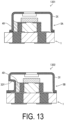
- FIG. 13 includes cross-sectional views of a light emitting device 5A and a light emitting device 5B in each of which the inner surface of the lid 3 and the first via conductor 142 are bonded with a bonding material 40.
- a lid 3X included in the light emitting device 5A indicated by reference numeral 1301 in FIG. 13 one of four side walls is located near the first via conductor 142 at ground potential.
- a lid 3Y included in the light emitting device 5B indicated by reference numeral 1302 in FIG. 13 has a recessed portion 32Y in which part of a side wall protrudes inward.
- the light emitting devices 5A and 5B illustrated in FIG. 13 by placing the inner surface of the lid 3 facing the first via conductor 142 close to the first via conductor 142, connection between the lid 3 and the first via conductor 142 is facilitated.
- the substrate 1 and the lid 3 have a rectangular shape when viewed in plan, but the substrate 1 and the lid 3 may have another shape such as circular or polygonal when viewed in plan.
- the substrate 1 may have multiple element mounting regions 13, and the lid 3 may have multiple windows 31.
- the light emitting device 5 includes the substrate 1 having a conductor resistance reduction effect and a heat dissipation effect or the package 4 including the substrate 1, an energy-saving effect or reliability as an electronic component can be improved.
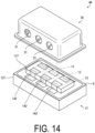
- FIG. 14 is an exploded perspective view of a package 4A.
- the package 4A includes a substrate 1T that is a variation of the substrate 1, and a lid 3A that is a variation of the lid 3.
- the substrate 1T has three element mounting regions 13 on a first substrate 11T, and can be used, for example, as a substrate on which three types of edge emitting LDs that respectively emit red (R) light, green (G) light, and blue (B) light are mounted as elements.
- the lid 3A has three windows 31 corresponding to the multiple elements.
- FIG. 14 illustrates an example in which the substrate 1T has three element mounting regions 13, but the number of the element mounting regions 13 is not limited to this example. The number of element mounting regions 13 that the substrate 1T has and the number of the windows 31 that the lid 3A has can be set freely.
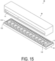
- FIG. 15 is an exploded perspective view of a package 4B.
- the package 4B includes a substrate 1U that is a variation of the substrate 1, and a lid 3B that is a variation of the lid 3.
- the substrate 1U has multiple element mounting regions 13 on a first substrate 11U, and has a rectangular shape elongated in an arrangement direction of the elements.
- the substrate 1U can be used, for example, as a substrate on which edge emitting LDs are mounted.
- the lid 3B has one window 31 for the multiple elements included in the first substrate 11U of the element.
- the window 31 of the lid 3B has a rectangular shape elongated in the arrangement direction of the elements.
- one window 31 may be provided in the lid 3B for the multiple elements.
Landscapes
- Engineering & Computer Science (AREA)
- Microelectronics & Electronic Packaging (AREA)
- Manufacturing & Machinery (AREA)
- Structure Of Printed Boards (AREA)
- Led Device Packages (AREA)
- Semiconductor Lasers (AREA)
Abstract
Description
- The present disclosure relates to a substrate, a package, an electronic component, and a light emitting device.
- Depending on a type or an application of an element, one method to raise a mounting position of the element is to mount the element on a surface of a protruding portion of a substrate having the protruding portion. For example, a light emitting module described in
Patent Document 1 includes a carrier (substrate) on which a semiconductor laser mounted on a submount (protruding portion) and a lens component are mounted. - Patent Document 1:
JP 2013-80900 A - In an aspect of the present disclosure, a substrate includes a first substrate having a first surface on which an element is to be mounted, a second surface opposite the first surface, and a first side surface connecting the first surface and the second surface, a second substrate larger than the first substrate and having a third surface supporting the first substrate and a fourth surface opposite the third surface, and first via conductors configured to electrically connect the first surface and the second surface and exposed on the first side surface of the first substrate from the first surface to the second surface.
- In an aspect of the present disclosure, a package includes the substrate and a lid.
- In an aspect of the present disclosure, an electronic component includes the substrate or the package, and an element mounted in the package.
- In an aspect of the present disclosure, a light emitting device includes the substrate or the package, and an element mounted in the package, in which the element is a light emitting element.
-
-
FIG. 1 is a perspective view of a substrate according to an embodiment of the present disclosure. -
FIG. 2 includes a top view, a cross-sectional view, side views, and a bottom view of the substrate. -
FIG. 3 is an exploded perspective view of the substrate. -
FIG. 4 is a top view of a first substrate included in the substrate. -
FIG. 5 is a schematic plan view schematically illustrating an outer edge of a first via conductor and a side of a first surface when an angle θ illustrated inFIG. 4 is changed. -
FIG. 6 includes a top view, a cross-sectional view, side views, and a bottom view of a substrate as a variation. -
FIG. 7 includes a top view, a cross-sectional view, side views, and a bottom view of a substrate as a variation. -
FIG. 8 includes a top view, a cross-sectional view, side views, and a bottom view of a substrate as a variation. -
FIG. 9 is an enlarged top view of a first substrate of the variation. -
FIG. 10 is a top view of a first substrate as a variation. -
FIG. 11 is an exploded perspective view of an electronic component including the substrate according to the embodiment of the present disclosure. -
FIG. 12 includes a top view, a cross-sectional view, and a side view of the electronic component. -
FIG. 13 includes cross-sectional views of exemplary light emitting devices in each of which an inner surface of a lid and a first via conductor are bonded with a bonding material. -
FIG. 14 is an exploded perspective view of another exemplary package. -
FIG. 15 is an exploded perspective view of another exemplary package. - An exemplary embodiment of the present disclosure will be described in detail below with reference to the accompanying drawings.
-
FIG. 1 is a perspective view of asubstrate 1 according to the present embodiment.FIG. 2 includes a top view, a cross-sectional view, side views, and a bottom view of thesubstrate 1. InFIG. 2 , a view indicated byreference numeral 201 is the top view of thesubstrate 1, and a view indicated byreference numeral 202 is the cross-sectional view taken along line I-I in the view indicated byreference numeral 201. InFIG. 2 , a view indicated byreference numeral 203 is a side view of thesubstrate 1 when viewed from a negative direction of an X-axis, and a view indicated byreference numeral 204 is a side view of thesubstrate 1 when viewed from a positive direction of a Y-axis. A view indicated byreference numeral 205 inFIG. 2 is the bottom view of thesubstrate 1.FIG. 3 is an exploded perspective view of thesubstrate 1.FIG. 4 is a top view of afirst substrate 11 included in thesubstrate 1. - In the accompanying drawings, the
substrate 1 is assumed to be located on an X-Y plane in a virtual XYZ space. In this specification, an upward direction refers to a positive direction of a virtual Z-axis. The terms "up/top" and "down/bottom" are used in the following description by way of convenience and are not to be construed as limiting in the actual use of thesubstrate 1 or the like. A thickness direction of thesubstrate 1 refers to the direction of the Z-axis. - The
substrate 1 is a substrate for mounting an element and functions as a support for supporting the element. Thesubstrate 1 can be used for mounting an element that requires heat dissipation and/or an element that requires reduction in conductor resistance. More specifically, thesubstrate 1 can be used for mounting, for example, an element such as a light emitting element such as a light emitting diode (LED) or a laser diode (LD), a light receiving element such as a photo diode (PD), a charge coupled device (CCD) type or a complementary metal oxide semiconductor (CMOS) type imaging element, or a sensor element such as an acceleration sensor. - As illustrated in
FIGs. 1 to 3 , thesubstrate 1 includes thefirst substrate 11 and asecond substrate 12 that supports thefirst substrate 11 and is larger than thefirst substrate 11. Specifically, when viewed in plan from the Z-axis direction, thesecond substrate 12 is larger than thefirst substrate 11. Therefore, part of athird surface 12A (upper surface) of thesecond substrate 12 is covered with thefirst substrate 11, and at least part of a surrounding area is not covered. Thefirst substrate 11 has, for example, a rectangular shape, and has afirst surface 11A having a region on which an element is to be mounted (hereinafter referred to as an element mounting region 13) and asecond surface 11B located opposite thefirst surface 11A. Thesecond substrate 12 has thethird surface 12A supporting thefirst substrate 11 and afourth surface 12B located opposite thethird surface 12A. Thefirst substrate 11 and thesecond substrate 12 have, for example, a rectangular shape. The shape of thefirst substrate 11 and thesecond substrate 12 is not limited to rectangular, and may be circular or polygonal. - The
element mounting region 13 is a region on which an element is to be mounted on thefirst surface 11A, and is a region indicated by dashed lines in each of the accompanying drawings. In the drawings, a shape of theelement mounting region 13 is square, but is not limited thereto, and may be a shape corresponding to a shape of an element to be mounted. - As the
first substrate 11 and thesecond substrate 12, a ceramic such as an aluminum oxide sintered body (alumina ceramic), an aluminum nitride sintered body, a silicon nitride sintered body, a mullite sintered body, or a glass ceramic sintered body can be used. When thefirst substrate 11 and thesecond substrate 12 are, for example, aluminum oxide sintered bodies, a slurry is prepared by adding and mixing a suitable organic binder, solvent, and the like with raw material powders such as aluminum oxide (Al2O3), silicon oxide (SiO2), magnesium oxide (MgO), and calcium oxide (CaO). A ceramic green sheet is produced by forming this slurry into a sheet by employing a well-known doctor blade method, calender roll method, or the like. Subsequently, this ceramic green sheet is subjected to an appropriate punching process, and multiple ceramic green sheets are stacked to form a green body, which is then fired at a high temperature (approximately 1600°C) to produce thefirst substrate 11 and thesecond substrate 12. -
Wiring conductors 14 are provided on the surface and inside of thesubstrate 1. For example, in the example illustrated inFIGs. 1 to 3 , thesubstrate 1 includesconnection pads 141, first viaconductors 142,wiring layers 143, second viaconductors 144, andterminal electrodes 145 as thewiring conductors 14. - The connection pads 141 for connection with an element are provided on an upper surface of the substrate 1 (
first surface 11A). Theterminal electrodes 145 for connection with an external electrical circuit are provided on a lower surface of the substrate 1 (fourth surface 12B). Theterminal electrodes 145 are not limited to being provided on the lower surface of thesubstrate 1, and may be provided on side surfaces from the lower surface or on the side surfaces of thesubstrate 1. Theseconnection pads 141 and theterminal electrodes 145 are electrically connected by thefirst via conductors 142, thewiring layers 143, and the second viaconductors 144 provided on the surface and inside of thesubstrate 1. - The
connection pads 141 and theterminal electrodes 145 mainly contain, for example, metals such as tungsten, molybdenum, manganese, copper, silver, palladium, gold, platinum, nickel, or cobalt, or alloys containing any of these metals as conductor materials. Theconnection pads 141 and theterminal electrodes 145 are formed on the surfaces of thesubstrate 1 as metal layers such as metallization layers or plating layers of a conductor material. The wiring layers 143 are formed inside thesubstrate 1 by metallization of a conductor material. Thefirst substrate 11 and thesecond substrate 12 are different in size. Thus, the wiring layers 143 placed between thefirst substrate 11 and thesecond substrate 12 may be exposed on the surface of thesecond substrate 12. - When the
connection pads 141, the wiring layers 143, and theterminal electrodes 145 are, for example, metallization layers of tungsten, they can be formed by printing a metal paste prepared by mixing tungsten powder with an organic solvent and an organic binder at predetermined positions on the ceramic green sheets to be thesubstrate 1 by a screen printing method or the like and firing the paste. A plating layer of nickel, gold, or the like may be further deposited on exposed surfaces of the metallization layers to serve as theconnection pads 141, the wiring layers 143, and theterminal electrodes 145 by using an electrolytic plating method, electroless plating method, or the like. - The first via
conductors 142 are via conductors that electrically connect thefirst surface 11A side and thesecond surface 11B side and are exposed on the side surfaces offirst substrate 11 from thefirst surface 11A to thesecond surface 11B. The first viaconductors 142 electrically connect conductors on thefirst surface 11A and conductors on thesecond surface 11B. To be specific, the first viaconductors 142 electrically connect theconnection pads 141 on thefirst surface 11A and the wiring conductors (wiring layers 143) on the second surface. The second viaconductors 144 are via conductors that electrically connect thethird surface 12A side and thefourth surface 12B side. The second viaconductors 144 electrically connect conductors on thethird surface 12A and conductors on thefourth surface 12B. To be specific, the second viaconductors 144 electrically connect the wiring layers 143 on thethird surface 12A and theterminal electrodes 145 on thefourth surface 12B. - The term via conductors may be used as a generic term for the first via
conductors 142 and the second viaconductors 144. That is, the via conductors are conductors passing through thefirst substrate 11 or thesecond substrate 12. The via conductors may be formed at predetermined positions in the ceramic green sheet prior to printing of the metal paste for forming theconnection pads 141, the wiring layers 143, and theterminal electrodes 145. For example, first, through holes for via conductors are formed in the ceramic green sheet for thefirst substrate 11 or thesecond substrate 12 by a machining method such as stamping using a die or punching or laser beam machining. Thereafter, the through holes are filled with a metallization paste for via conductors by the above printing method, and the via conductors are formed by firing together with the ceramic green sheet for thefirst substrate 11 or thesecond substrate 12. The metallization paste is prepared by kneading the metal powder described above with an appropriate solvent and binder to adjust viscosity to an appropriate level. The metallization paste may contain glass powder or ceramic powder in order to increase bonding strength with thefirst substrate 11 or thesecond substrate 12. The via conductors other than the first viaconductors 142 have, for example, a circular shape when viewed in plan from the Z-axis direction. That is, for example, in thefirst substrate 11 of the present embodiment, the second viaconductors 144 are cylindrical. However, the shape of the via conductors is not limited to cylindrical, and may be oval, polygonal, or prismatic, for example. - In the example illustrated in
FIGs. 1 to 3 , all of the via conductors included in thefirst substrate 11 are the first viaconductors 142, but thefirst substrate 11 may include via conductors that are not exposed on the side surfaces of thefirst substrate 11. - The first via
conductors 142 have, for example, a semi-circular shape when viewed in plan from the Z-axis direction. That is, the first viaconductors 142 may be, for example, semi-cylindrical. The shape of the first viaconductors 142 when viewed in plan is not limited to semi-circular, and may be semi-elliptical or rectangular. When the shape of the first viaconductors 142 as viewed in plan is a shape without corners such as a semi-circular shape or a semi-elliptical shape, the likelihood of cracks in thefirst substrate 11 originating from the corners can be reduced. The sizes of the multiple first viaconductors 142 included in thefirst substrate 11 may be different from each other. - The first via
conductors 142 may be formed as follows, for example. That is, (i) in the ceramic green sheet to be thefirst substrate 11, forming via conductors based on positions of the first viaconductors 142 in thefirst substrate 11. (ii) Punching out thefirst substrate 11 such that at least part of the via conductors is exposed on the side surfaces of thefirst substrate 11 using a die corresponding to the shape of thefirst substrate 11. For example, the first viaconductors 142 having a semi-cylindrical shape can be formed by forming cylindrical via conductors in (i) and punching out in (ii). The exposed surfaces of the first viaconductors 142 may be further coated with a plating layer of nickel, gold, or the like using an electrolytic plating method, an electroless plating method, or the like. - The step (ii) may be performed after the ceramic green sheet to be the
second substrate 12 is positioned below the ceramic green sheet to be thefirst substrate 11, with thefirst substrate 11 and thesecond substrate 12 aligned, so that they have a predetermined positional relationship. In this case, an appropriate binder obtained by adding and mixing a resin, a solvent, and the like may be applied to a portion to be thesecond surface 11B of thefirst substrate 11, and a portion to be thefirst substrate 11 may be pressed against the portion to be thethird surface 12A of thesecond substrate 12 for adhesion while punching out the portion to be thefirst substrate 11. Thus, by punching out the ceramic green sheet to be thefirst substrate 11 from above using a die, the punching process of the portion to be thefirst substrate 11 and the stacking step of the portion to be thefirst substrate 11 and the portion to be thesecond substrate 12 may be performed simultaneously. By simultaneously performing the punching process and the stacking step, positional accuracy when mounting thefirst substrate 11 on thesecond substrate 12 may be improved. - When the
substrate 1 is used to mount an element described above, thesubstrate 1 is required to have low conductor resistance and high heat dissipation in the wiring included in thesubstrate 1. In thesubstrate 1 according to the present embodiment, theconnection pads 141 connected to the element and theterminal electrodes 145 are connected by the via conductors having wider cross-sectional areas than connection wires or the like, thereby achieving low conductor resistance. The via conductors included in thefirst substrate 11 close to the element are exposed on the side surfaces of thefirst substrate 11, which provide excellent heat dissipation. - Since the
first substrate 11 is smaller than thesecond substrate 12, an area occupied by thewiring conductors 14 is relatively large with respect to an area of thefirst substrate 11 in a horizontal cross section of thefirst substrate 11 when viewed in plan. Therefore, when the via conductors are formed inside the first substrate, distances between the via conductors and the side surfaces of thefirst substrate 11 may be insufficient depending on the positions of the via conductors. Cracks may occur in thefirst substrate 11 at locations where the distance between the outer edge of the via conductor and the side surface of thefirst substrate 11 is not sufficient. However, the first viaconductors 142 of the present embodiment are exposed from thefirst surface 11A to thesecond surface 11B, which reduces a possibility of such cracks. Even when other through-hole conductors need to be provided in order to mount a semiconductor element, a capacitor, or the like other than the element described above on the first substrate, wiring layout flexibility can be improved while reducing the possibility of cracks. - As illustrated in
FIG. 2 , the first viaconductors 142 have portions overlapping the second viaconductors 144 when viewed in plan. With this configuration, heat and current conduction paths are formed in straight lines and with large cross-sectional areas from thefirst surface 11A on which the element is mounted to thefourth surface 12B connected to the mounting substrate, further improving heat dissipation and an effect of reducing conductor resistance. As illustrated inFIG. 2 , in thesubstrate 1, the cross-sectional area of the second viaconductors 144 is larger than the cross-sectional area of the first viaconductors 142. With such a configuration, heat transfer paths from thefirst surface 11A to thefourth surface 12B also extend in the X-Y plane direction, so heat is transferred to thefourth surface 12B while diffusing in the X-Y plane direction. Thus, heat dissipation can be further improved. - Here, positioning of the first via
conductor 142 on thefirst substrate 11 will be described.FIG. 4 is a top view of thefirst substrate 11.FIG. 5 is a schematic plan view schematically illustrating an outer edge of the first viaconductor 142 and a side of thefirst surface 11A when an angle θ illustrated inFIG. 4 is changed. - As illustrated in
FIG. 4 , thefirst substrate 11 may include the first viaconductors 142 at the centers of opposite sides of thefirst surface 11A. This configuration increases a distance L between the first viaconductor 142 and a side at which the first viaconductor 142 is not located, thereby reducing a possibility of cracks in thefirst substrate 11 due to stress such as thermal stress caused by heat generated during use. The distance L can be defined as the shortest distance from the side where the first viaconductor 142 is not located to a position where an extension line orthogonal to the side intersects the outer edge of the first viaconductor 142. In manufacturing thesubstrate 1, when punching out the ceramic green sheet to be thefirst substrate 11, the distances between the outer edges of thefirst substrate 11 and the outer edges of the first viaconductors 142 are large, so cracks are less likely to occur in thefirst substrate 11. - Here, when the
first substrate 11 is viewed in plan, attention will be paid to an intersection of the outer edge of the first viaconductor 142 and the side of thefirst surface 11A in a case where the shape of the first viaconductor 142 is semi-circular or semi-elliptical when viewed in plan. An angle between a tangent to the outer edge of the first viaconductor 142 at the intersection and the side of thefirst surface 11A is defined as an angle θ. In thefirst substrate 11, the angle θ may be from 70° to 110° (90° ± 20°). By setting the angle θ from 70° to 110°, the conductor cross section of the first viaconductor 142 does not become small, and a thin portion (narrow portion) is less likely to be formed in thefirst substrate 11 between the first viaconductor 142 and the side surface of thefirst substrate 11. Thus, thefirst substrate 11 has low conductor resistance and the likelihood of chipping or the like of thefirst substrate 11 at the narrow portion is reduced, resulting in a substrate with high connection reliability. First Variation
FIG. 6 includes a top view, a cross-sectional view, side views, and a bottom view of asubstrate 1P that is a variation of thesubstrate 1. InFIG. 6 , a view indicated byreference numeral 601 is the top view of thesubstrate 1P, and a view indicated byreference numeral 602 is the cross-sectional view taken along line II-II in the view indicated byreference numeral 601. InFIG. 6 , a view indicated byreference numeral 603 is a side view of thesubstrate 1P when viewed from the negative direction of the X-axis, and a view indicated byreference numeral 604 is a side view of thesubstrate 1P when viewed from the positive direction of the Y-axis. A view indicated byreference numeral 605 inFIG. 6 is the bottom view of thesubstrate 1P. - A
first substrate 11P according to a first variation includes first viaconductors 142P. A cross-sectional area of the first viaconductors 142P in a cross section parallel to thefirst surface 11A increases from thefirst surface 11A toward thesecond surface 11B. The cross-sectional area may increase stepwise from thefirst surface 11A toward thesecond surface 11B, or may gradually increase from thefirst surface 11A toward thesecond surface 11B. When the cross-sectional area gradually increases from thefirst surface 11A toward thesecond surface 11B, there are no corners where stress tends to concentrate between thefirst substrate 11P and the first viaconductors 142P, thereby improving connection reliability. - The above configuration of the first via
conductors 142P improves heat dissipation because heat from the element is transferred to the second substrate side while diffusing in a plane direction as well. Connection areas between the first viaconductors 142P and the wiring layers 143 on asecond substrate 12P are increased, thereby improving connection reliability. The large conduction cross-sectional area further reduces the conductor resistance compared with the first viaconductors 142. - The
second substrate 12P of thesubstrate 1P includes second viaconductors 144P. The cross-sectional area of the second viaconductors 144P in a cross section parallel to thethird surface 12A increases from the third surface toward the fourth surface. With this configuration, a heat dissipation effect and a conductor resistance reduction effect in thesecond substrate 12 are further improved. -
FIG. 7 includes a top view, a cross-sectional view, side views, and a bottom view of asubstrate 1Q that is a variation of thesubstrate 1. InFIG. 7 , a view indicated byreference numeral 701 is the top view of thesubstrate 1Q, and a view indicated byreference numeral 702 is a cross-sectional view taken along line III-III in the view indicated byreference numeral 701. InFIG. 7 , a view indicated byreference numeral 703 is a side view of thesubstrate 1Q when viewed from the positive direction of the X-axis, and a view indicated byreference numeral 704 is a side view of thesubstrate 1Q when viewed from the positive direction of the Y-axis. A view indicated byreference numeral 705 inFIG. 7 is the bottom view of thesubstrate 1Q. - Side surfaces of a first substrate 11Q according to a second variation are inclined, and an angle θP between the side surfaces and the
third surface 12A is an obtuse angle. Surfaces of the first viaconductors 142Q exposed on the side surfaces of the first substrate 11Q may be flush with the side surfaces of the first substrate 11Q, and the exposed surfaces of the first viaconductors 142Q may also be inclined. The angle between the exposed surfaces and thethird surface 12A may be the same as the angle θP between the side surfaces and thethird surface 12A. The angle θP is not limited, and may be, for example, from 95° to 110°. When the angle θP is in a range from 95° to 110°, the first viaconductors 142Q in their entireties in a length direction are easily exposed on the side surfaces of the first substrate 11Q, thereby easily improving heat dissipation. The inclined surfaces of the first substrate 11Q can be formed, for example, by providing a clearance between dies in the step of punching out the ceramic green sheet to be the first substrate 11Q. To be more specific, the inclined surfaces can be formed by setting a diameter (length of one side) of a support die (female die) installed on a punching end surface side of the first substrate 11Q to be larger than a diameter (length of one side) of a punching die (male die) installed on a punching start surface side of the first substrate 11Q. The inclination angle (angle θP) of the first substrate 11Q can be adjusted by changing the size of the clearance between the male die and the female die. - In the
substrate 1Q, the angle θP between the side surfaces of the first substrate 11Q and thethird surface 12A is an obtuse angle, which reduces a possibility of cracks originating from the corners. This reduces the likelihood of disconnection of the wiring, thereby improving reliability. Thesubstrate 1Q in which the angle θP is an obtuse angle has excellent heat dissipation because areas of the first viaconductors 142Q exposed to the side surfaces of the first substrate 11Q are larger than that of the substrate in which the angle θP is a right angle. The first viaconductors 142Q further increase a conductor cross-sectional area and increase thermal diffusion in a lateral direction, which further improves a conductor resistance reduction effect and a heat dissipation effect. -
FIG. 8 includes a top view, a cross-sectional view, side views, and a bottom view of asubstrate 1R that is a variation of thesubstrate 1. InFIG. 8 , a view indicated byreference numeral 801 is the top view of thesubstrate 1R, and a view indicated byreference numeral 802 is a cross-sectional view taken along line IV-IV in the view indicated byreference numeral 801. InFIG. 8 , a view indicated byreference numeral 803 is a side view of thesubstrate 1R when viewed from the negative direction of the X-axis, and a view indicated byreference numeral 804 is a side view of thesubstrate 1R when viewed from the positive direction of the Y-axis. A view indicated byreference numeral 805 inFIG. 8 is the bottom view of thesubstrate 1R.FIG. 9 is an enlarged top view of afirst substrate 11R. - The
substrate 1R according to a third variation has a rectangular shape, and includes first viaconductors 142R at opposite corners of thefirst surface 11A. With this configuration, the distance between outer edges of the first viaconductors 142R can be increased, thereby reducing the likelihood of cracks occurring in a portion between the first viaconductors 142R of thefirst substrate 11R. By ensuring this distance, the likelihood of short circuit between the conductors can be reduced. Diameters of the first viaconductors 142R can be increased, which further improves a conductor resistance reduction effect and a heat dissipation effect. - Here, attention is paid to intersections between the outer edges of the first via
conductor 142R and the sides of thefirst surface 11A. Two angles (angles θ1 and θ2) between tangents to the outer edges of the first viaconductor 142R at the intersections and the sides of thefirst surface 11A may be different from each other. The angles θ1 and θ2 may each be from 70° to 110° (90° ± 20°). -
FIG. 10 is a top view of afirst substrate 11S that is a variation of thefirst substrate 11. As illustrated inFIG. 10 , thefirst substrate 11S includes two first via conductors 142S1 and 142S2 of different sizes. The first via conductor 142S1 has a semi-elliptical shape, and part of the first via conductor 142S1 overlaps theelement mounting region 13 when viewed in plan. - With the above configuration, the region overlapping the
element mounting region 13 when viewed in plan is larger than that in the embodiment and variations described above. Consequently, heat dissipation can be further improved. In this case, the first via conductor 142S1 having a larger cross-sectional area may be used as ground potential, and the first via conductor 142S2 having a smaller cross-sectional area may be used as potential for power extraction. The first via conductor 142S1 may be connected to a wiring conductor through, for example, an electrically conductive bonding material (solder, brazing material, electrically conductive adhesive, etc.) placed on a lower surface of thefirst substrate 11S. On the other hand, the first via conductor 142S2 may be connected to a wiring conductor through a bonding wire. Alternately, one first via conductor 142S1 having a larger cross-sectional area may be provided only for heat dissipation, and two first via conductors 142S2 having a smaller cross-sectional area may be provided for electrical connection. - In the embodiment described above, an example in which the
first substrate 11 and thesecond substrate 12 each have a single layer has been described. However, thefirst substrate 11 and thesecond substrate 12 may be a stacked body in which two or more insulating layers are stacked. By stacking the multiple insulating layers, a complicated wiring structure can be easily provided. - When the
first substrate 11 and thesecond substrate 12 are stacked bodies in which multiple insulating layers are stacked, via conductors may be defined as conductors passing through the insulating layers. For example, an internal wiring layer may be provided between the insulating layers. In this case, theconnection pad 141 and theterminal electrode 145 may be electrically connected by the first viaconductor 142, thewiring layer 143, the internal wiring layer, and the second viaconductor 144. - An electronic component according to the present disclosure includes the
substrate 1 according to the present disclosure and an element. In the following, as an example, a case in which the element is alight emitting element 2, that is, a case in which the electronic component is a light emittingdevice 5 will be described. -
FIG. 11 is an exploded perspective view illustrating thelight emitting device 5.FIG. 12 includes a top view, a cross-sectional view, and a side view of thelight emitting device 5. InFIG. 12 , a view indicated byreference numeral 1201 is the top view of thelight emitting device 5. InFIG. 12 , a view indicated byreference numeral 1202 is the cross-sectional view taken along line V-V in the view indicated byreference numeral 1201. InFIG. 12 , a view indicated byreference numeral 1203 is the side view of thelight emitting device 5 as viewed from a negative X-axis negative direction. - The
light emitting device 5 includes thesubstrate 1 and thelight emitting element 2. As illustrated inFIG. 11 , when thelight emitting element 2 is required to be hermetically sealed, thelight emitting device 5 may include alid 3. A configuration including thesubstrate 1 and thelid 3 is referred to as apackage 4. That is, thelight emitting device 5 can be said to include thepackage 4 and thelight emitting element 2. - In the
light emitting device 5, thelight emitting element 2 mounted on thesubstrate 1 and an external electrical circuit are electrically connected by electrically connecting theterminal electrodes 145 provided, for example, on the lower surface of thesubstrate 1 to the external electrical circuit. In other words, thelight emitting element 2 and the external electrical circuit are electrically connected to each other via thewiring conductors 14. - The
light emitting element 2 and theconnection pads 141 may be connected using connection members such as bonding wires, or may be flip-chip connected by solder or the like through terminals provided on a lower surface of thelight emitting element 2. Alternatively, these connection methods may be used in combination. - Although not illustrated, the
light emitting device 5 may include another semiconductor element and/or a passive element such as a capacitor in addition to thelight emitting element 2, when needed. These components may be mounted on thefirst surface 11A of thefirst substrate 11 or thethird surface 12A of thesecond substrate 12. Other semiconductor elements may include, for example, integrated circuits such as an application specific integrated circuit (ASIC). For example, the semiconductor element and/or the capacitor may be electrically connected to thelight emitting element 2 and thesubstrate 1 by connection members such as bonding wires, or may be connected to thewiring conductors 14 of thesubstrate 1 by soldering. - In the example illustrated in
FIG. 11 , thelight emitting element 2 is sealed and protected by thelid 3. In the example illustrated inFIG. 11 , thelight emitting device 5 includes thelid 3 that is box-shaped (cap-shaped) and collectively covers thelight emitting element 2, thefirst substrate 11, and the wiring layers 143 on the upper surface of thesecond substrate 12. - The
lid 3 is made of a material such as metal or resin, and is bonded to thesubstrate 1. Thelid 3 may be bonded through a sealing bonding material. Examples of the sealing bonding material include, for example a resin adhesive, glass, and a brazing material including solder. When thelid 3 and thesubstrate 1 are bonded with a brazing material, abonding metal layer 6 may be provided on the upper surface of thesecond substrate 12 so as to surround thefirst substrate 11 and the wiring layers 143 on the upper surface of thesecond substrate 12. When thelid 3 is made of metal, thelid 3 may be bonded to thebonding metal layer 6 on thesecond substrate 12 by welding such as seam welding or laser welding. In the case of bonding using the brazing material or the like, an overall heating by reflow heating is performed, whereas in the case of bonding by seam welding or laser welding, local heating of only the bonding portion can be performed. Since thelight emitting element 2 is mounted on thefirst substrate 11, a space corresponding to the thickness of thefirst substrate 11 and a distance from the outer edge of thefirst substrate 11 to the inner edge of thebonding metal layer 6 is ensured. Thus, thelight emitting element 2 can be separated by a large distance from thebonding metal layer 6 to be heated during bonding. Therefore, influence of heat on thelight emitting element 2 can be reduced. Thebonding metal layer 6 may be formed of, for example a metal film such as a plating film, a metallization layer, or the like. When thelid 3 is made of a material having low wettability (bondability) with a brazing material, such as resin, the bonding metal layer may also be formed on thelid 3. - The
lid 3 includes awindow 31 on an upper surface for emitting light. For example, thewindow 31 may be made by closing anopening portion 310 formed at a predetermined position of thelid 3 with aglass plate 311 that transmits light. Thelid 3 can be used to mount a surface emitting LD such as a surface emitting LED or a vertical cavity surface emitting laser (VCSEL). Although the shape of thewindow 31 is circular inFIG. 11 , the shape of thewindow 31 is not limited to being circular, and may be rectangular, polygonal, or the like. The size of thewindow 31 may also be changed as appropriate. Theopening portion 310 may be provided on the upper surface or a side surface of thelid 3 depending on the direction in which thelight emitting element 2 emits light. - In the
light emitting device 5, thebonding metal layer 6 may be connected to ground potential, and thebonding metal layer 6 and the electricallyconductive lid 3 made of metal or the like may be bonded or welded with an electrically conductive bonding material. With this configuration, thelid 3 is at ground potential, thereby providing a magnetic shield effect for the elements mounted inside thelid 3. - The shield effect can also be obtained by connecting an inner surface of the
lid 3 and the first viaconductor 142 with an electrically conductive bonding material. In this case, a metal bonding material such as solder may be used as a bonding material for connecting the inner surface of thelid 3 and the first viaconductor 142. The metal bonding material such as solder has excellent thermal conductivity, allowing thelid 3 to serve as a radiator, which also improves heat dissipation. -
FIG. 13 includes cross-sectional views of alight emitting device 5A and alight emitting device 5B in each of which the inner surface of thelid 3 and the first viaconductor 142 are bonded with abonding material 40. In alid 3X included in thelight emitting device 5A indicated byreference numeral 1301 inFIG. 13 , one of four side walls is located near the first viaconductor 142 at ground potential. Alid 3Y included in thelight emitting device 5B indicated byreference numeral 1302 inFIG. 13 has a recessedportion 32Y in which part of a side wall protrudes inward. As in thelight emitting devices FIG. 13 , by placing the inner surface of thelid 3 facing the first viaconductor 142 close to the first viaconductor 142, connection between thelid 3 and the first viaconductor 142 is facilitated. - In the example illustrated in
FIG. 11 , thesubstrate 1 and thelid 3 have a rectangular shape when viewed in plan, but thesubstrate 1 and thelid 3 may have another shape such as circular or polygonal when viewed in plan. Thesubstrate 1 may have multipleelement mounting regions 13, and thelid 3 may havemultiple windows 31. - Since the
light emitting device 5 includes thesubstrate 1 having a conductor resistance reduction effect and a heat dissipation effect or thepackage 4 including thesubstrate 1, an energy-saving effect or reliability as an electronic component can be improved. -
FIG. 14 is an exploded perspective view of apackage 4A. Thepackage 4A includes asubstrate 1T that is a variation of thesubstrate 1, and alid 3A that is a variation of thelid 3. - The
substrate 1T has threeelement mounting regions 13 on afirst substrate 11T, and can be used, for example, as a substrate on which three types of edge emitting LDs that respectively emit red (R) light, green (G) light, and blue (B) light are mounted as elements. Thelid 3A has threewindows 31 corresponding to the multiple elements. -
FIG. 14 illustrates an example in which thesubstrate 1T has threeelement mounting regions 13, but the number of theelement mounting regions 13 is not limited to this example. The number ofelement mounting regions 13 that thesubstrate 1T has and the number of thewindows 31 that thelid 3A has can be set freely. -
FIG. 15 is an exploded perspective view of apackage 4B. Thepackage 4B includes a substrate 1U that is a variation of thesubstrate 1, and alid 3B that is a variation of thelid 3. - The substrate 1U has multiple
element mounting regions 13 on a first substrate 11U, and has a rectangular shape elongated in an arrangement direction of the elements. The substrate 1U can be used, for example, as a substrate on which edge emitting LDs are mounted. Thelid 3B has onewindow 31 for the multiple elements included in the first substrate 11U of the element. Thewindow 31 of thelid 3B has a rectangular shape elongated in the arrangement direction of the elements. As in the case of thelid 3B, when distances between the elements mounted on the substrate 1U are small, onewindow 31 may be provided in thelid 3B for the multiple elements. When the linearity of light emitted from each of the elements is high and appropriate clearances are ensured between the elements, adjacent light beams do not interfere with each other even when thewindow 31 has one rectangular shape for the multiple elements. - In the present disclosure, the invention has been described above based on the various drawings and examples. However, the invention according to the present disclosure is not limited to each embodiment described above. That is, the embodiments of the invention according to the present disclosure can be modified in various ways within the scope illustrated in the present disclosure, and embodiments obtained by appropriately combining the technical means disclosed in different embodiments are also included in the technical scope of the invention according to the present disclosure. In other words, a person skilled in the art can easily make various variations or modifications based on the present disclosure. Note that these variations or modifications are included within the scope of the present disclosure.
-
- 1, 1P, 1Q, 1R, 1T Substrate
- 11, 11P, 11Q, 11R, 11S, 11T, 11U First substrate
- 11A First surface
- 11B Second surface
- 12, 12P, 12Q, 12R, 12T, 12U Second substrate
- 12A Third surface
- 12B Fourth surface
- 13 Element mounting region
- 14 Wiring conductor
- 141 Connection pad
- 142, 142P, 142Q, 142R, 142S1, 142S2 First via conductor
- 143 Wiring layer
- 144, 144P Second via conductor
- 145 Terminal electrode
- 2 Light emitting element (element)
- 3, 3A, 3B Lid
- 4, 4A, 4B Package
- 5, 5A, 5B Light emitting device (electronic component)
Claims (11)
- A substrate comprising:a first substrate having a first surface on which an element is to be mounted, a second surface located opposite the first surface, and a first side surface connecting the first surface and the second surface;a second substrate larger than the first substrate and having a third surface supporting the first substrate and a fourth surface located opposite the third surface; andfirst via conductors configured to electrically connect the first surface and the second surface and exposed on the first side surface of the first substrate from the first surface to the second surface.
- The substrate according to claim 1, wherein
a cross-sectional area of the first via conductors in a cross section parallel to the first surface increases from the first surface toward the second surface. - The substrate according to claim 2, wherein
the first side surface of the first substrate is inclined, and an angle between the first side surface and the third surface is an obtuse angle. - The substrate according to any one of claims 1 to 3, whereinthe first substrate has a rectangular shape, andthe first via conductors are located at respective centers of opposite sides of the first surface.
- The substrate according to any one of claims 1 to 3, whereinthe first substrate has a rectangular shape, andthe first via conductors are respectively located at opposite corners of the first surface.
- The substrate according to any one of claims 1 to 5, wherein
when viewed in plan, an angle between a tangent to an outer edge of each of the first via conductors at an intersection of the outer edge of each of the first via conductors and a side of the first surface and the side of the first surface is 90° ± 20°. - The substrate according to any one of claims 1 to 6, wherein
at least one of the first via conductors has a portion overlapping a region where the element is to be mounted when viewed in plan. - The substrate according to any one of claims 1 to 7, whereinthe second substrate comprises second via conductors configured to electrically connect the third surface and the fourth surface, andat least one of the first via conductors has a portion overlapping one of the second via conductors when viewed in plan.
- A package comprising:the substrate according to any one of claims 1 to 8; anda lid.
- An electronic component comprising:the substrate according to any one of claims 1 to 8 or the package according to claim 9; andan element mounted in the package.
- A light emitting device comprising:the substrate according to any one of claims 1 to 8 or the package according to claim 9; andan element mounted in the package, whereinthe element is a light emitting element.
Applications Claiming Priority (2)
| Application Number | Priority Date | Filing Date | Title |
|---|---|---|---|
| JP2021074366 | 2021-04-26 | ||
| PCT/JP2022/018247 WO2022230731A1 (en) | 2021-04-26 | 2022-04-20 | Substrate, package, electronic component, and light emitting device |
Publications (2)
| Publication Number | Publication Date |
|---|---|
| EP4333044A1 true EP4333044A1 (en) | 2024-03-06 |
| EP4333044A4 EP4333044A4 (en) | 2025-07-02 |
Family
ID=83847042
Family Applications (1)
| Application Number | Title | Priority Date | Filing Date |
|---|---|---|---|
| EP22795644.8A Pending EP4333044A4 (en) | 2021-04-26 | 2022-04-20 | SUBSTRATE, HOUSING, ELECTRONIC COMPONENT AND LIGHT-EMITTING DEVICE |
Country Status (5)
| Country | Link |
|---|---|
| US (1) | US20240213433A1 (en) |
| EP (1) | EP4333044A4 (en) |
| JP (1) | JP7587025B2 (en) |
| CN (1) | CN117178353A (en) |
| WO (1) | WO2022230731A1 (en) |
Families Citing this family (1)
| Publication number | Priority date | Publication date | Assignee | Title |
|---|---|---|---|---|
| JPWO2025023251A1 (en) * | 2023-07-24 | 2025-01-30 |
Family Cites Families (9)
| Publication number | Priority date | Publication date | Assignee | Title |
|---|---|---|---|---|
| JP2003298204A (en) * | 2002-03-29 | 2003-10-17 | Fujitsu Ltd | Component mounting structure |
| JP2005035864A (en) * | 2002-10-15 | 2005-02-10 | Kenichiro Miyahara | Light-emitting element mounting substrate |
| JP2005191135A (en) * | 2003-12-24 | 2005-07-14 | Kawaguchiko Seimitsu Co Ltd | Semiconductor package |
| US20080224786A1 (en) * | 2007-03-13 | 2008-09-18 | Stolpman James L | Apparatus and method for temperature compensating an ovenized oscillator |
| US20090073713A1 (en) * | 2007-09-07 | 2009-03-19 | Glovatsky Andrew Z | LED Multidimensional Printed Wiring Board Using Standoff Boards |
| US8355766B2 (en) * | 2007-10-12 | 2013-01-15 | Masimo Corporation | Ceramic emitter substrate |
| JP2012080085A (en) * | 2010-09-10 | 2012-04-19 | Nichia Chem Ind Ltd | Support medium and light emitting device using the same |
| US8821042B2 (en) | 2011-07-04 | 2014-09-02 | Sumitomo Electic Industries, Ltd. | Optical module with lens assembly directly mounted on carrier by soldering and laser diode indirectly mounted on carrier through sub-mount |
| RU2019106302A (en) * | 2016-08-10 | 2020-09-16 | Киосера Корпорейшн | ELECTRIC ELEMENT MOUNTING HOUSING, MATRIX HOUSING AND ELECTRICAL DEVICE |
-
2022
- 2022-04-20 CN CN202280029309.6A patent/CN117178353A/en active Pending
- 2022-04-20 WO PCT/JP2022/018247 patent/WO2022230731A1/en not_active Ceased
- 2022-04-20 JP JP2023517466A patent/JP7587025B2/en active Active
- 2022-04-20 US US18/556,509 patent/US20240213433A1/en active Pending
- 2022-04-20 EP EP22795644.8A patent/EP4333044A4/en active Pending
Also Published As
| Publication number | Publication date |
|---|---|
| WO2022230731A1 (en) | 2022-11-03 |
| JPWO2022230731A1 (en) | 2022-11-03 |
| EP4333044A4 (en) | 2025-07-02 |
| JP7587025B2 (en) | 2024-11-19 |
| CN117178353A (en) | 2023-12-05 |
| US20240213433A1 (en) | 2024-06-27 |
Similar Documents
| Publication | Publication Date | Title |
|---|---|---|
| CN106062946B (en) | Electronic unit storage packaging part and electronic device | |
| JP2009071013A (en) | Light emitting device mounting board | |
| JP4981696B2 (en) | package | |
| CN114204405A (en) | Package for mounting optical element, electronic device, and electronic module | |
| CN110943151A (en) | Package for mounting light-emitting element, light-emitting device, and light-emitting module | |
| JP6140834B2 (en) | Wiring board and electronic device | |
| JP2014127678A (en) | Wiring board and electronic device | |
| WO2020045480A1 (en) | Wiring board, electronic device and electronic module | |
| EP4333044A1 (en) | Substrate, package, electronic component, and light emitting device | |
| JP2014157949A (en) | Wiring board and electronic device | |
| KR102425194B1 (en) | Package | |
| US10249564B2 (en) | Electronic component mounting substrate, electronic device, and electronic module | |
| JP2022173218A (en) | Substrate for mounting light-emitting element, and light-emitting device | |
| US11784117B2 (en) | Wiring board, electronic device, and electronic module | |
| JP2004281996A (en) | Light emitting element storage package and light emitting device | |
| JP6626735B2 (en) | Electronic component mounting board, electronic device and electronic module | |
| JP6166194B2 (en) | Wiring board, electronic device and electronic module | |
| JP4070195B2 (en) | Light emitting element storage package | |
| EP4012760A1 (en) | Package for mounting optical element, electronic device, and electronic module | |
| JP2014049590A (en) | Wiring board and electronic device | |
| JPWO2018097313A1 (en) | Wiring board, electronic device and electronic module | |
| EP3905314A1 (en) | Wiring substrate, electronic device, and electronic module | |
| CN110291628B (en) | Wiring substrate, electronic device and electronic module | |
| JP2007227739A (en) | Electronic component storage package and electronic component device | |
| JP6166094B2 (en) | Wiring board and electronic device |
Legal Events
| Date | Code | Title | Description |
|---|---|---|---|
| STAA | Information on the status of an ep patent application or granted ep patent |
Free format text: STATUS: THE INTERNATIONAL PUBLICATION HAS BEEN MADE |
|
| PUAI | Public reference made under article 153(3) epc to a published international application that has entered the european phase |
Free format text: ORIGINAL CODE: 0009012 |
|
| STAA | Information on the status of an ep patent application or granted ep patent |
Free format text: STATUS: REQUEST FOR EXAMINATION WAS MADE |
|
| 17P | Request for examination filed |
Effective date: 20231020 |
|
| AK | Designated contracting states |
Kind code of ref document: A1 Designated state(s): AL AT BE BG CH CY CZ DE DK EE ES FI FR GB GR HR HU IE IS IT LI LT LU LV MC MK MT NL NO PL PT RO RS SE SI SK SM TR |
|
| DAV | Request for validation of the european patent (deleted) | ||
| DAX | Request for extension of the european patent (deleted) | ||
| A4 | Supplementary search report drawn up and despatched |
Effective date: 20250530 |
|
| RIC1 | Information provided on ipc code assigned before grant |
Ipc: H05K 1/14 20060101ALN20250523BHEP Ipc: H01S 5/0222 20210101ALN20250523BHEP Ipc: H10H 20/858 20250101ALI20250523BHEP Ipc: H10H 20/857 20250101ALI20250523BHEP Ipc: H01S 5/02315 20210101ALI20250523BHEP Ipc: H01L 23/12 20060101AFI20250523BHEP |