EP4332531A1 - Sensor member and physical quantity sensor - Google Patents
Sensor member and physical quantity sensor Download PDFInfo
- Publication number
- EP4332531A1 EP4332531A1 EP23193398.7A EP23193398A EP4332531A1 EP 4332531 A1 EP4332531 A1 EP 4332531A1 EP 23193398 A EP23193398 A EP 23193398A EP 4332531 A1 EP4332531 A1 EP 4332531A1
- Authority
- EP
- European Patent Office
- Prior art keywords
- protective film
- sensor member
- electrode portion
- electrode
- peripheral edge
- Prior art date
- Legal status (The legal status is an assumption and is not a legal conclusion. Google has not performed a legal analysis and makes no representation as to the accuracy of the status listed.)
- Pending
Links
- 230000001681 protective effect Effects 0.000 claims abstract description 169
- 230000002093 peripheral effect Effects 0.000 claims abstract description 53
- 238000001514 detection method Methods 0.000 claims abstract description 28
- 229910052751 metal Inorganic materials 0.000 claims abstract description 25
- 239000002184 metal Substances 0.000 claims abstract description 25
- 239000000758 substrate Substances 0.000 claims description 8
- 239000012790 adhesive layer Substances 0.000 claims description 6
- 229910052802 copper Inorganic materials 0.000 claims description 4
- 229910052737 gold Inorganic materials 0.000 claims description 4
- 229910052763 palladium Inorganic materials 0.000 claims description 4
- 229910052709 silver Inorganic materials 0.000 claims description 4
- 150000004767 nitrides Chemical class 0.000 claims description 3
- 239000010408 film Substances 0.000 description 215
- 239000012528 membrane Substances 0.000 description 25
- 238000000034 method Methods 0.000 description 11
- 229910052804 chromium Inorganic materials 0.000 description 9
- 239000012530 fluid Substances 0.000 description 9
- 229910052782 aluminium Inorganic materials 0.000 description 7
- 239000010409 thin film Substances 0.000 description 7
- 238000007740 vapor deposition Methods 0.000 description 6
- 238000009429 electrical wiring Methods 0.000 description 5
- 238000004544 sputter deposition Methods 0.000 description 5
- 230000015572 biosynthetic process Effects 0.000 description 4
- 238000000059 patterning Methods 0.000 description 4
- VYPSYNLAJGMNEJ-UHFFFAOYSA-N Silicium dioxide Chemical compound O=[Si]=O VYPSYNLAJGMNEJ-UHFFFAOYSA-N 0.000 description 3
- 239000000463 material Substances 0.000 description 3
- 238000012986 modification Methods 0.000 description 3
- 230000004048 modification Effects 0.000 description 3
- 229910052750 molybdenum Inorganic materials 0.000 description 3
- 229910052757 nitrogen Inorganic materials 0.000 description 3
- 229910052760 oxygen Inorganic materials 0.000 description 3
- 238000003825 pressing Methods 0.000 description 3
- 229910052719 titanium Inorganic materials 0.000 description 3
- 229910052581 Si3N4 Inorganic materials 0.000 description 2
- MCMNRKCIXSYSNV-UHFFFAOYSA-N Zirconium dioxide Chemical compound O=[Zr]=O MCMNRKCIXSYSNV-UHFFFAOYSA-N 0.000 description 2
- 238000000137 annealing Methods 0.000 description 2
- 238000005530 etching Methods 0.000 description 2
- 229910052732 germanium Inorganic materials 0.000 description 2
- 238000005259 measurement Methods 0.000 description 2
- 150000002739 metals Chemical class 0.000 description 2
- 229910052759 nickel Inorganic materials 0.000 description 2
- PXHVJJICTQNCMI-UHFFFAOYSA-N nickel Substances [Ni] PXHVJJICTQNCMI-UHFFFAOYSA-N 0.000 description 2
- 229910052755 nonmetal Inorganic materials 0.000 description 2
- 229910052710 silicon Inorganic materials 0.000 description 2
- 229910052814 silicon oxide Inorganic materials 0.000 description 2
- 229910001220 stainless steel Inorganic materials 0.000 description 2
- 229910000838 Al alloy Inorganic materials 0.000 description 1
- -1 AlO3 Inorganic materials 0.000 description 1
- 229910000990 Ni alloy Inorganic materials 0.000 description 1
- XUIMIQQOPSSXEZ-UHFFFAOYSA-N Silicon Chemical compound [Si] XUIMIQQOPSSXEZ-UHFFFAOYSA-N 0.000 description 1
- 229910000831 Steel Inorganic materials 0.000 description 1
- 230000001133 acceleration Effects 0.000 description 1
- 229910045601 alloy Inorganic materials 0.000 description 1
- 239000000956 alloy Substances 0.000 description 1
- 229910052787 antimony Inorganic materials 0.000 description 1
- 229910052785 arsenic Inorganic materials 0.000 description 1
- 229910052788 barium Inorganic materials 0.000 description 1
- 229910052790 beryllium Inorganic materials 0.000 description 1
- 229910052797 bismuth Inorganic materials 0.000 description 1
- 229910052796 boron Inorganic materials 0.000 description 1
- 229910052791 calcium Inorganic materials 0.000 description 1
- 229910052799 carbon Inorganic materials 0.000 description 1
- 238000006243 chemical reaction Methods 0.000 description 1
- 229910052681 coesite Inorganic materials 0.000 description 1
- 229910052906 cristobalite Inorganic materials 0.000 description 1
- 230000000694 effects Effects 0.000 description 1
- 238000010292 electrical insulation Methods 0.000 description 1
- 229910052735 hafnium Inorganic materials 0.000 description 1
- 238000010438 heat treatment Methods 0.000 description 1
- 229910052738 indium Inorganic materials 0.000 description 1
- 238000009413 insulation Methods 0.000 description 1
- 229910052741 iridium Inorganic materials 0.000 description 1
- 229910052742 iron Inorganic materials 0.000 description 1
- 239000010410 layer Substances 0.000 description 1
- 229910052745 lead Inorganic materials 0.000 description 1
- 229910052749 magnesium Inorganic materials 0.000 description 1
- 229910052748 manganese Inorganic materials 0.000 description 1
- 238000004519 manufacturing process Methods 0.000 description 1
- 229910052758 niobium Inorganic materials 0.000 description 1
- 229910052762 osmium Inorganic materials 0.000 description 1
- 229910052698 phosphorus Inorganic materials 0.000 description 1
- 238000000206 photolithography Methods 0.000 description 1
- 229910052697 platinum Inorganic materials 0.000 description 1
- 238000004881 precipitation hardening Methods 0.000 description 1
- 229910052761 rare earth metal Inorganic materials 0.000 description 1
- 229910052702 rhenium Inorganic materials 0.000 description 1
- 229910052703 rhodium Inorganic materials 0.000 description 1
- 229910052707 ruthenium Inorganic materials 0.000 description 1
- 229910052711 selenium Inorganic materials 0.000 description 1
- 230000035945 sensitivity Effects 0.000 description 1
- 238000007493 shaping process Methods 0.000 description 1
- 239000010703 silicon Substances 0.000 description 1
- 239000000377 silicon dioxide Substances 0.000 description 1
- HQVNEWCFYHHQES-UHFFFAOYSA-N silicon nitride Chemical compound N12[Si]34N5[Si]62N3[Si]51N64 HQVNEWCFYHHQES-UHFFFAOYSA-N 0.000 description 1
- 239000010935 stainless steel Substances 0.000 description 1
- 229910001256 stainless steel alloy Inorganic materials 0.000 description 1
- 239000010959 steel Substances 0.000 description 1
- 229910052682 stishovite Inorganic materials 0.000 description 1
- 229910052712 strontium Inorganic materials 0.000 description 1
- 229910052714 tellurium Inorganic materials 0.000 description 1
- 229910052716 thallium Inorganic materials 0.000 description 1
- 229910052718 tin Inorganic materials 0.000 description 1
- 229910052905 tridymite Inorganic materials 0.000 description 1
- 229910052721 tungsten Inorganic materials 0.000 description 1
- 229910052725 zinc Inorganic materials 0.000 description 1
- 229910052726 zirconium Inorganic materials 0.000 description 1
Images


Classifications
-
- G—PHYSICS
- G01—MEASURING; TESTING
- G01L—MEASURING FORCE, STRESS, TORQUE, WORK, MECHANICAL POWER, MECHANICAL EFFICIENCY, OR FLUID PRESSURE
- G01L19/00—Details of, or accessories for, apparatus for measuring steady or quasi-steady pressure of a fluent medium insofar as such details or accessories are not special to particular types of pressure gauges
- G01L19/06—Means for preventing overload or deleterious influence of the measured medium on the measuring device or vice versa
- G01L19/0627—Protection against aggressive medium in general
-
- G—PHYSICS
- G01—MEASURING; TESTING
- G01L—MEASURING FORCE, STRESS, TORQUE, WORK, MECHANICAL POWER, MECHANICAL EFFICIENCY, OR FLUID PRESSURE
- G01L9/00—Measuring steady of quasi-steady pressure of fluid or fluent solid material by electric or magnetic pressure-sensitive elements; Transmitting or indicating the displacement of mechanical pressure-sensitive elements, used to measure the steady or quasi-steady pressure of a fluid or fluent solid material, by electric or magnetic means
- G01L9/0041—Transmitting or indicating the displacement of flexible diaphragms
- G01L9/0051—Transmitting or indicating the displacement of flexible diaphragms using variations in ohmic resistance
- G01L9/0052—Transmitting or indicating the displacement of flexible diaphragms using variations in ohmic resistance of piezoresistive elements
- G01L9/0055—Transmitting or indicating the displacement of flexible diaphragms using variations in ohmic resistance of piezoresistive elements bonded on a diaphragm
-
- G—PHYSICS
- G01—MEASURING; TESTING
- G01L—MEASURING FORCE, STRESS, TORQUE, WORK, MECHANICAL POWER, MECHANICAL EFFICIENCY, OR FLUID PRESSURE
- G01L19/00—Details of, or accessories for, apparatus for measuring steady or quasi-steady pressure of a fluent medium insofar as such details or accessories are not special to particular types of pressure gauges
- G01L19/0061—Electrical connection means
- G01L19/0069—Electrical connection means from the sensor to its support
-
- G—PHYSICS
- G01—MEASURING; TESTING
- G01L—MEASURING FORCE, STRESS, TORQUE, WORK, MECHANICAL POWER, MECHANICAL EFFICIENCY, OR FLUID PRESSURE
- G01L9/00—Measuring steady of quasi-steady pressure of fluid or fluent solid material by electric or magnetic pressure-sensitive elements; Transmitting or indicating the displacement of mechanical pressure-sensitive elements, used to measure the steady or quasi-steady pressure of a fluid or fluent solid material, by electric or magnetic means
- G01L9/02—Measuring steady of quasi-steady pressure of fluid or fluent solid material by electric or magnetic pressure-sensitive elements; Transmitting or indicating the displacement of mechanical pressure-sensitive elements, used to measure the steady or quasi-steady pressure of a fluid or fluent solid material, by electric or magnetic means by making use of variations in ohmic resistance, e.g. of potentiometers, electric circuits therefor, e.g. bridges, amplifiers or signal conditioning
- G01L9/04—Measuring steady of quasi-steady pressure of fluid or fluent solid material by electric or magnetic pressure-sensitive elements; Transmitting or indicating the displacement of mechanical pressure-sensitive elements, used to measure the steady or quasi-steady pressure of a fluid or fluent solid material, by electric or magnetic means by making use of variations in ohmic resistance, e.g. of potentiometers, electric circuits therefor, e.g. bridges, amplifiers or signal conditioning of resistance-strain gauges
Definitions
- the present invention relates to a physical quantity sensor and a sensor member constituting the physical quantity sensor.
- sensor members constituting physical quantity sensors such as a pressure sensor
- a sensor member that is formed on a metal base through a film formation step and the like.
- sensor members there are sensor members requiring high reliability even in a harsh environment such as a high temperature and high humidity environment.
- a technique for providing a protective film that protects a detection portion has been proposed as a technique for improving the reliability of a sensor member (refer to JP 2005-249520 A ).
- JP 2005-249520 A since an electrode for ensuring electrical connection with the detection portion cannot completely cover the protective film and the like, moisture or the like may intrude through an interface between the electrode and the protective film, which becomes a challenge in improving reliability.
- Patent Document 1 JP 2005-249520 A
- the present invention has been conceived in view of such circumstances, and an object of the present invention is to provide a sensor member capable of suitably preventing a problem such as the intrusion of moisture or the like through an interface between an electrode and a protective film.
- a sensor member including: a protected portion provided on one surface of a metal base and including a detection portion; a protective film including a first protective film portion having a first thickness and a second protective film portion having a second thickness thicker than the first thickness and formed at an opening peripheral edge of an opening leading to the protected portion, and covering at least a part of the protected portion from above; and an electrode portion including a first electrode portion disposed in the opening and connected to the protected portion, and a second electrode portion connected to the first electrode portion at an outer peripheral edge of the first electrode portion and formed on the second protective film portion.
- the protective film includes the second protective film portion with a thick thickness around the opening for connecting the electrode portion to the protected portion.
- an outer electrode surface of the electrode portion which does not face the protective film and an outer protective film surface of the protective film which does not face the electrode portion may be connected at an outer peripheral edge of an interface between the electrode portion and the protective film without forming a step.
- the outer electrode surface and the outer protective film surface are connected at the outer peripheral edge of the interface without forming a step, the problem that moisture accumulated on the step intrudes into the interface can be suitably prevented, and the reliability can be enhanced.
- an outer peripheral edge of the second electrode portion which is also an outer peripheral edge of the electrode portion may coincide with an outer peripheral edge of the second protective film portion.
- the protective film may be transitionally changed in thickness from the first thickness at a connection position with the first protective film portion to the second thickness at a connection position with the second protective film portion, and may include a third protective film portion connecting the first protective film portion and the second protective film portion.
- the electrode portion may comprises at least one of Au, Ag, Cu, and Pd.
- the adhesiveness of the electrode portion to the protective film that is relatively soft can be enhanced.
- the electrode portion since such an electrode portion is chemically stable, the electrode portion contributes to improving the reliability of the sensor member.
- the protective film may comprises at least one of an oxide, a nitride, and an oxynitride.
- Such a protective film has high strength, the structural strength particularly at the periphery of the opening can be improved, and the reliability of the sensor member can be improved.
- an adhesive layer may be formed at an interface between the electrode portion and the protective film.
- the protected portion may include an insulating film covering the one surface from above, and a strain-resistance film formed on the insulating film and constituting the detection portion.
- the strain-resistance film constitutes the detection portion while the insulating film ensures insulation from the metal base, and such a sensor member can detect a physical quantity associated with a deformation of the metal base, even in a harsh environment such as a high temperature and high humidity environment.
- the detection portion may detect a pressure acting on the metal base.
- Such a sensor member realizes a pressure sensor with high reliability capable of performing stable detection even when installed in a harsh environment such as a high temperature and high humidity environment for a long period of time.
- FIG. 1 is a schematic cross-sectional view of a pressure sensor 10 using a sensor member 18 according to one embodiment of the present invention.
- the pressure sensor 10 includes a stem 20 having a hollow cylindrical shape.
- the stem 20 is made of, for example, metal such as steel, aluminum alloy, stainless steel, or nickel alloy.
- the stem 20 includes a membrane 22 constituting an end wall disposed at one end of the hollow cylinder, and the membrane 22 undergoes deformation corresponding to pressure.
- the membrane 22 constitutes a metal base on which a detection portion 33 and the like of the sensor member 18 are provided.
- the metals described above as the material of the stem 20 can be used, and particularly, austenitic stainless steels such as SUS304 and SUS316, precipitation hardening stainless steels such as SUS630 and SUS631, and the like are preferably used from the viewpoint of durability at high temperatures or the like.
- the other end of the stem 20 is an open end of a hollow portion, and the hollow portion of the stem 20 communicates with a flow path 12b of a connection member 12.
- a fluid introduced into the flow path 12b is guided from the hollow portion of the stem 20 to an inner surface 22a that is the other surface of the membrane 22, and the fluid pressure acts on the membrane 22.
- a flange portion 21 is formed around the open end of the stem 20 to protrude outward from an axis of the stem 20.
- the flange portion 21 is sandwiched between the connection member 12 and a pressing member 14, so that the flow path 12b leading to the inner surface 22a of the membrane 22 is sealed.
- connection member 12 includes a thread groove 12a for fixing the pressure sensor 10.
- the pressure sensor 10 is fixed to a pressure chamber or the like in which the fluid as a measurement object is enclosed, through the thread groove 12a. Accordingly, the flow path 12b formed inside the connection member 12 and the inner surface 22a of the membrane 22 of the stem 20 airtightly communicate with the pressure chamber in which the fluid as a measurement object exists.
- a circuit substrate 16 is attached to an upper surface of the pressing member 14.
- the circuit substrate 16 has a ring shape surrounding a periphery of the stem 20; however, the shape of the circuit substrate 16 is not limited to this shape.
- a circuit and the like to which a detection signal from the sensor member 18 is transmitted are built-in in the circuit substrate 16.
- the sensor member 18 is formed on an end surface of the stem 20.
- FIG. 2 is a plan view of an end surface portion of the stem 20 illustrated in FIG. 1 , when viewed from above.
- the sensor member 18 includes a protective film 40 and electrode portions 50 exposed from the protective film 40.
- the sensor member 18 includes a protected portion 30 protected from an external environment by the protective film 40.
- the protected portion 30 is disposed below the protective film 40 and the electrode portions 50.
- the protected portion 30 includes the detection portion 33 that detects a pressure.
- the electrode portions 50 and the circuit substrate 16 are connected by intermediate wirings 72 through wire bonding or the like.
- the illustration of the intermediate wirings 72 is omitted in FIG. 2 .
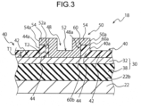
- FIG. 3 is a cross-sectional view of the sensor member 18 taken along sectional line III-III illustrated in FIG. 2 .
- the sensor member 18 will be described mainly with reference to FIGS. 2 and 3 .
- the protected portion 30 including the detection portion 33 (refer to FIG. 2 ) is provided on an outer surface 22b that is one surface of the membrane 22 as the metal base.
- the protected portion 30 is disposed between the membrane 22 and the protective film 40, is shielded from the fluid and the like therebelow by the membrane 22, and is protected from an external environment, in which the sensor member 18 is provided, by the protective film 40 thereabove.
- the protected portion 30 includes an insulating film 38 and a strain-resistance film 32.
- the insulating film 38 covers the outer surface 22b of the membrane 22 as the metal base from above.
- the insulating film 38 is located between the membrane 22 therebelow and the strain-resistance film 32 thereabove to ensure electrical insulation between the membrane 22 and the strain-resistance film 32.
- the insulating film 38 is formed to cover substantially the entirety of the outer surface 22b of the membrane 22.
- the insulating film 38 is composed of, for example, an insulating film made of silicon oxide, silicon nitride, silicon oxynitride, or the like.
- a thickness of the insulating film 38 is preferably 10 ⁇ m or less, further preferably 1 to 5 ⁇ m.
- the insulating film 38 can be formed on the outer surface 22b of the membrane 22, for example, by a vapor deposition method such as CVD.
- the strain-resistance film 32 is formed on the insulating film 38, and constitutes the detection portion 33 illustrated in FIG. 2 .
- a first resistor R1, a second resistor R2, a third resistor R3, and a fourth resistor R4 are formed in a predetermined pattern.
- the first to fourth resistors R1, R2, R3, and R4 generate strain corresponding to the deformation of the membrane 22, and are changed in resistance according to the deformation of the membrane 22.
- the first to fourth resistors R1 to R4 are connected by electrical wirings 34 formed on the same strain-resistance film 32, so as to constitute a Wheatstone bridge circuit as the detection portion 33.
- the detection portion 33 can detect a fluid pressure that is the pressure of the fluid acting on the membrane 22 that is a metal member.
- the first to fourth resistors R1, R2, R3, and R4 of the sensor member 18 illustrated in FIG. 2 are provided at positions where the membrane 22 illustrated in FIGS. 1 and 2 is deformed and strained by the fluid pressure, and are configured such that the resistances change according to the strain amounts thereof.
- the pressure sensor 10 illustrated in FIG. 1 can receive an output of the detection portion 33 of the sensor member 18 or supply electric power from a power supply unit to the sensor member 18, via the circuit substrate 16.
- the strain-resistance film 32 including the first to fourth resistors R1, R2, R3, and R4 illustrated in FIG. 2 can be produced, for example, by patterning a conductive thin film made of a predetermined material.
- the strain-resistance film 32 contains, for example, Cr and Al, preferably contains 50 to 99 at% of Cr and 1 to 50 at% of Al, and further preferably contains 70 to 90 at% of Cr and 5 to 30 at% of Al. Since the strain-resistance film 32 contains Cr and Al, the temperature coefficient of resistance (TCR) or temperature coefficient of sensitivity (TCS) under a high temperature environment is stable and highly accurate pressure detection can be performed. In addition, both a high gauge factor and good temperature stability can be achieved at a higher level by setting the amounts of Cr and Al within predetermined ranges.
- the strain-resistance film 32 may contain an element other than Cr and Al, and for example, the strain-resistance film 32 may contain O or N.
- O or N contained in the strain-resistance film 32 which is not completely removed and remains in a reaction chamber when the strain-resistance film 32 is formed, may be incorporated into the strain-resistance film 32.
- O or N contained in the strain-resistance film 32 may be intentionally introduced into the strain-resistance film 32 by being used as an atmospheric gas during film formation or during annealing.
- the strain-resistance film 32 may contain a metal element other than Cr and Al.
- the strain-resistance film 32 may contain a small amount of a metal or non-metal element other than Cr and Al, and heat treatment such as annealing may be performed, so that the gauge factor or temperature property is improved.
- Examples of the metal and non-metal elements other than Cr and Al contained in the strain-resistance film 32 include Ti, Nb, Ta, Ni, Zr, Hf, Si, Ge, C, P, Se, Te, Zn, Cu, Bi, Fe, Mo, W, As, Sn, Sb, Pb, B, Ge, In, Tl, Ru, Rh, Re, Os, Ir, Pt, Pd, Ag, Au, Co, Be, Mg, Ca, Sr, Ba, Mn, and rare earth elements.
- the strain-resistance film 32 can be formed by a thin film method such as sputtering or vapor deposition.
- the first to fourth resistors R1, R2, R3, and R4 can be formed, for example, by patterning a thin film into a meandering shape.
- the thickness of the strain-resistance film 32 is not particularly limited, and is preferably 10 ⁇ m or less, further preferably 0.1 to 1 ⁇ m.
- the electrical wirings 34 are formed by patterning the strain-resistance film 32.
- the electrical wirings 34 can also be formed from a conductive film or layer different from the strain-resistance film 32.
- the protective film 40 is formed on the protected portion 30, and covers at least a part of the protected portion 30 from above. As illustrated in FIGS. 2 and 3 , openings 48 in which the electrode portions 50 are formed are formed in the protective film 40. As illustrated in FIG. 2 , the protective film 40 is formed to cover the entirety of an upper surface of the strain-resistance film 32 of the protected portion 30 except for portions at which the openings 48 are formed. Incidentally, in FIG. 2 , for the purpose of the description of the disposition of the protective film 40, the protective film 40 is hatched with oblique lines, and the shapes of the detection portion 33 and the like formed in the protected portion 30 below the protective film 40 are illustrated through the protective film 40 by dotted lines.
- the protective film 40 includes a first protective film portion 42 having a first thickness T1, and second protective film portions 44 having a second thickness T2 thicker than the first thickness T1.
- the second protective film portions 44 are formed at opening peripheral edges 48a of the openings 48 leading to the protected portion 30.
- the first protective film portion 42 is formed at a portion other than the opening peripheral edges 48a of the openings 48 at which the second protective film portions 44 are formed. Namely, in the protective film 40, the thickness (second thickness T2) of portions around the openings 48 is thicker than the thickness (first thickness T1) of the other portion away from the openings 48.
- the second protective film portions 44 are formed, for example, in regions within approximately 10 ⁇ m from outer edges of the openings 48.
- the first protective film portion 42 is formed, for example, in a region that is away from the outer edges of the openings 48 by approximately 10 ⁇ m or more.
- the first thickness T1 and the second thickness T2 are average thicknesses of the first protective film portion 42 and the second protective film portions 44, and the film thicknesses of the first protective film portion 42 and the second protective film portions 44 do not necessarily need to be constant.
- the first thickness T1 of the first protective film portion 42 of the protective film 40 can be set to, for example, approximately 10 to 1000 nm, preferably approximately 100 to 300 nm.
- the second thickness T2 of the second protective film portions 44 of the protective film 40 can be set to, for example, approximately 101 to 300%, preferably approximately 106 to 150% of the first thickness T1.
- the distance that an interface 60 between the protective film 40 and the electrode portions 50 shields the protected portion 30 can be lengthened by setting the second thickness T2 to be thicker than the first thickness T1; however, when the second thickness T2 is too thick, it takes too much time to form the protective film 40, which is a problem.
- the protective film 40 is composed of, for example, an insulating film similarly to the insulating film 38.
- the insulating film constituting the protective film 40 include films made of an oxide, a nitride, and an oxynitride, and these films are preferably used from the viewpoint of improving the strength of the protective film 40. More specifically, examples of the material constituting the protective film 40 include SiO 2 , SiON, Si 3 N 4 , AlO 3 , and ZrO 2 .
- the protective film 40 can be formed on the strain-resistance film 32 that is a part of the protected portion 30, for example, by a vapor deposition method such as CVD, sputtering, or the like; however, the method for forming the protective film 40 is not particularly limited.
- the electrode portion 50 is formed inside the opening 48 of the protective film 40 and at the opening peripheral edge 48a of the opening 48. As illustrated in FIG. 2 , in the sensor member 18, the electrode portions 50 are formed at four locations to correspond to the openings 48 of the protective film 40. However, the number and disposition of the electrode portions 50 included in the sensor member 18 are not limited only to the example illustrated in FIG. 2 .
- the electrode portion 50 includes a first electrode portion 52 disposed in the opening 48 and connected to the strain-resistance film 32 of the protected portion 30, and a second electrode portion 54 connected to the first electrode portion 52 at an outer peripheral edge 52a of the first electrode portion 52 and formed on the second protective film portion 44.
- the first electrode portion 52 is a portion of the electrode portion 50 which is disposed inside the opening peripheral edge 48a of the protective film 40 when the sensor member 18 is viewed from above.
- a lower portion of the first electrode portion 52 is disposed in the inside of the opening 48 which is a region inside the opening peripheral edge 48a and lower than an upper end of the second protective film portion 44, and a lower end of the first electrode portion 52 is in contact with the strain-resistance film 32.
- an upper portion of the first electrode portion 52 is disposed in a region higher than the upper end of the second protective film portion 44, and is connected to the second electrode portion 54.
- the second electrode portion 54 is a portion of the electrode portion 50 which is disposed outside the outer edge of the opening 48 when the sensor member 18 is viewed from above. As illustrated in FIG. 3 , the second electrode portion 54 is provided on the second protective film portion 44, and is connected to the first electrode portion 52 on an inner side, the first electrode portion 52 being disposed in the opening 48.
- the interface 60 between the electrode portion 50 and the protective film 40 (second protective film portion 44) is formed between the outer peripheral edge 52a of the first electrode portion 52 and an inner wall of the opening 48 and between a lower end surface of the second electrode portion 54 and an upper end surface of the second protective film portion 44. Therefore, the interface 60 between the electrode portion 50 and the protective film 40 is continuous from an inner edge 60b facing the protected portion 30 to an outer peripheral edge 60a of an upper surface of the sensor member 18.
- an outer electrode surface 50a of the electrode portion 50 which does not face the protective film 40 and an outer protective film surface 40a of the protective film 40 which does not face the electrode portion 50 are connected at the outer peripheral edge 60a of the interface 60 without forming a step. Since a step is not formed at the outer peripheral edge 60a of the interface 60, and the outer electrode surface 50a and the outer protective film surface 40a are smoothly connected, in the sensor member 18, moisture or the like can be prevented from accumulating at the outer peripheral edge 60a of the interface 60, and moisture or the like can be more suitably prevented from intruding from the interface 60 into the protected portion 30.
- an outer peripheral edge 54a of the second electrode portion 54 which is also an outer peripheral edge of the electrode portion 50 coincides with an outer peripheral edge 44a of the second protective film portion 44.
- the thickness of the protective film 40 is thin at a position where the protective film 40 coincides with the outer peripheral edge of the electrode portion 50, the problem that a depression or the like where moisture or the like is likely to accumulate is formed at the outer peripheral edge 60a of the interface 60 can be prevented.
- the electrode portion 50 is composed of a conductive film or the like made of metal or the like; however, the electrode portion 50 may contain any one of Au, Ag, Cu, and Pd.
- the adhesiveness of the electrode portion 50 to the protective film 40 that is relatively soft can be enhanced.
- the electrode portion 50 since the electrode portion 50 is chemically stable, the electrode portion 50 contributes to improving the reliability of the sensor member 18.
- a thickness of the electrode portion 50 can be set to, for example, 50 to 500 nm, and is preferably set to 100 to 300 nm.
- the electrode portion 50 can be formed, for example, by a thin film method such as sputtering or a vapor deposition method.
- the sensor member 18 illustrated in FIG. 3 and the like can be manufactured, for example, by the following manufacturing method.
- the strain-resistance film 32 is formed on an upper surface of the insulating film 38.
- the strain-resistance film 32 is formed, for example, by a thin film method such as vapor deposition or sputtering.
- the shape of the strain-resistance film 32 including the first to fourth resistors R1, R2, R3, and R4, the electrical wirings 34, and the like illustrated in FIG. 2 is formed by performing patterning through photolithography or the like.
- the protective film 40 is formed to cover the strain-resistance film 32 from above.
- the openings 48 that expose parts of the strain-resistance film 32 as illustrated in FIG. 3 is formed in the protective film 40.
- the protective film 40 is also formed by a thin film method such as CVD, vapor deposition, or sputtering.
- the protective film 40 including the openings 48 can be formed by lift-off, etching, or the like.
- the electrode portions 50 are formed by forming a metal film on the strain-resistance film 32 and the protective film 40 using a thin film method, and then by shaping an outer peripheral edge of the metal film.
- the shape of the protective film 40 as illustrated in FIG. 3 including the second protective film portions 44 having a thick thickness at the opening peripheral edges 48a is formed.
- the sensor member 18 is obtained through such steps.
- the shapes of the first protective film portion 42, the second protective film portions 44, and the electrode portions 50 as illustrated in FIGS. 2 and 3 can be formed, for example, by lift-off, etching, or the like.
- the protective film 40 includes the second protective film portion 44 with a thick thickness around the opening 48 for connecting the electrode portion 50 to the protected portion 30.
- the sensor member 18 described with reference to FIGS. 1 to 3 is merely one embodiment of the present invention, and it goes without saying that the technical scope of the present invention includes many other embodiments or modification examples.
- the detection portion 33 of the sensor member 18 detects a pressure acting on the membrane 22 as the metal base; however, the detection portion 33 is not limited only to detecting a pressure, and may detect physical quantities other than the pressure, such as strain, acceleration, torque, and inclination. Physical quantity sensors other than the pressure sensor can be configured by using such a sensor member.
- an adhesive layer may be formed at the interface 60 between the electrode portion 50 and the protective film 40.
- the adhesive layer includes films containing Cr, Ti, Ni, Mo, and the like, and the film thickness can be set to, for example, approximately 1 to 50 nm, preferably approximately 5 to 20 nm.
- FIG. 4 is a cross-sectional view of a periphery of an electrode portion 150 of a sensor member 118 according to a modification example.
- the sensor member 118 differs from the sensor member 18 illustrated in FIG. 3 in that a protective film 140 includes a third protective film portion 146 and an outer electrode surface 150a of the electrode portion 150 is inclined, but is the same as the sensor member 18 in the other aspects.
- the points of difference from the sensor member 18 will be mainly described, and the description of the points in common with the sensor member 18 will be omitted.
- the sensor member 118 includes the membrane 22 and the protected portion 30 including the detection portion 33 that are the same as those of the sensor member 18 illustrated in FIGS. 1 to 3 .
- the protective film 140 of the sensor member 118 includes a first protective film portion 142 having the first thickness T1 and a second protective film portion 144 having the second thickness T2 and formed at the opening peripheral edge 48a of the opening 48 leading to the protected portion 30.
- the protective film 140 illustrated in FIG. 4 covers the upper surface of the strain-resistance film 32 except for a portion at which the opening 48 is formed.
- the protective film 140 includes the third protective film portion 146 connecting the first protective film portion 142 and the second protective film portion 144.
- the third protective film portion 146 is transitionally changed in thickness from the first thickness T1 at a first connection position 146a with the first protective film portion 142 to the second thickness T2 at a second connection position 146b with the second protective film portion 144.
- the second protective film portion 144 is formed at the opening peripheral edge 48a of the opening 48 leading to the protected portion 30.
- the third protective film portion 146 is formed to surround an outer periphery of the second protective film portion 144, and the first protective film portion 142 is formed at a portion other than the opening peripheral edge 48a at which the second protective film portion 144 is formed and other than a portion around the opening peripheral edge 48a at which the third protective film portion 146 is formed.
- the electrode portion 150 of the sensor member 118 includes the first electrode portion 52 disposed in the opening 48 and connected to the strain-resistance film 32 of the protected portion 30, and a second electrode portion 154 connected to the first electrode portion 52 at the outer peripheral edge of the first electrode portion 52 and formed on the second protective film portion 144.
- an outer peripheral edge of the second electrode portion 154 which is also an outer peripheral edge of the electrode portion 150 coincides with an outer peripheral edge of the second protective film portion 144.
- An interface 160 between the electrode portion 150 and the protective film 140 is continuous from an inner edge 160b facing the protected portion 30 to an outer peripheral edge 160a of an upper surface of the sensor member 118.
- the outer electrode surface 150a of the electrode portion 150 which is a surface not facing the protective film 140 and an outer protective film surface 140a of the protective film 140 which is a surface not facing the electrode portion 150 are connected at the outer peripheral edge 160a of the interface 160 without forming a step parallel to the interface 160 inside the outer peripheral edge 160a.
- the outer protective film surface 140a of the protective film 140 is inclined in the vicinity of the outer peripheral edge 160a of the interface 160 by the third protective film portion 146.
- the outer electrode surface 150a of the electrode portion 150 is also inclined in the vicinity of the outer peripheral edge 160a of the interface 160. Accordingly, in the sensor member 118 as well, similarly to the sensor member 18, the outer electrode surface 150a and the outer protective film surface 140a are smoothly connected.
- the difference in inclination between the outer electrode surface 150a and the outer protective film surface 140a at the periphery of the interface 160 is not particularly limited, but is preferably set to, for example, 0 to 45 degrees from the viewpoint of preventing the intrusion of moisture or the like from the interface 160.
- the sensor member 118 illustrated in FIG. 4 since the thickness of the protective film 140 changes gently, the occurrence of cracks due to the concentration of stress in the protective film 140 can be more suitably prevented, and the reliability can be enhanced. In addition, regarding the points of common with the sensor member 18, the sensor member 118 has the same effects as the sensor member 18.
Landscapes
- Physics & Mathematics (AREA)
- General Physics & Mathematics (AREA)
- Chemical & Material Sciences (AREA)
- Analytical Chemistry (AREA)
- Pressure Sensors (AREA)
- Measuring Fluid Pressure (AREA)
Abstract
There is provided a sensor member capable of suitably preventing a problem such as the intrusion of moisture or the like through an interface between an electrode and a protective film. A sensor member includes: a protected portion provided on one surface of a metal base and including a detection portion; a protective film including a first protective film portion having a first thickness and a second protective film portion having a second thickness thicker than the first thickness and formed at an opening peripheral edge of an opening leading to the protected portion, and covering at least a part of the protected portion from above; and an electrode portion including a first electrode portion disposed in the opening and connected to the protected portion, and a second electrode portion connected to the first electrode portion at an outer peripheral edge of the first electrode portion and formed on the second protective film portion.
Description
- The present invention relates to a physical quantity sensor and a sensor member constituting the physical quantity sensor.
- As sensor members constituting physical quantity sensors such as a pressure sensor, there is known a sensor member that is formed on a metal base through a film formation step and the like. Among such sensor members, there are sensor members requiring high reliability even in a harsh environment such as a high temperature and high humidity environment.
- A technique for providing a protective film that protects a detection portion has been proposed as a technique for improving the reliability of a sensor member (refer to
JP 2005-249520 A - Patent Document 1:
JP 2005-249520 A - The present invention has been conceived in view of such circumstances, and an object of the present invention is to provide a sensor member capable of suitably preventing a problem such as the intrusion of moisture or the like through an interface between an electrode and a protective film.
- According to the present invention, there is provided a sensor member including: a protected portion provided on one surface of a metal base and including a detection portion; a protective film including a first protective film portion having a first thickness and a second protective film portion having a second thickness thicker than the first thickness and formed at an opening peripheral edge of an opening leading to the protected portion, and covering at least a part of the protected portion from above; and an electrode portion including a first electrode portion disposed in the opening and connected to the protected portion, and a second electrode portion connected to the first electrode portion at an outer peripheral edge of the first electrode portion and formed on the second protective film portion.
- In the sensor member according to the present invention, as can be understood from a relationship between the second protective film portion and the second electrode portion, since the electrode portion is formed on the protective film, an area of the opening formed in the protective film can be made narrower than an exposed area of the electrode portion when viewed from above. In addition, the protective film includes the second protective film portion with a thick thickness around the opening for connecting the electrode portion to the protected portion. In the sensor member having such a structure, since the distance that an interface between the protective film and the electrode portion shields the protected portion is long, the interface being formed at a periphery of the opening, a problem such as the intrusion of moisture or the like through the interface can be suitably prevented.
- In addition, for example, an outer electrode surface of the electrode portion which does not face the protective film and an outer protective film surface of the protective film which does not face the electrode portion may be connected at an outer peripheral edge of an interface between the electrode portion and the protective film without forming a step.
- Since the outer electrode surface and the outer protective film surface are connected at the outer peripheral edge of the interface without forming a step, the problem that moisture accumulated on the step intrudes into the interface can be suitably prevented, and the reliability can be enhanced.
- In addition, for example, when viewed from above, an outer peripheral edge of the second electrode portion which is also an outer peripheral edge of the electrode portion may coincide with an outer peripheral edge of the second protective film portion.
- In such a sensor member, since the thickness of the protective film is thin at a position where the protective film coincides with the outer peripheral edge of the electrode portion, the problem that a depression or the like where moisture or the like is likely to accumulate is formed at the outer peripheral edge of the interface can be prevented.
- In addition, for example, the protective film may be transitionally changed in thickness from the first thickness at a connection position with the first protective film portion to the second thickness at a connection position with the second protective film portion, and may include a third protective film portion connecting the first protective film portion and the second protective film portion.
- In such a sensor member, since the thickness of the protective film changes gently, the occurrence of cracks due to the concentration of stress in the protective film can be more suitably prevented, and the reliability can be enhanced.
- In addition, for example, the electrode portion may comprises at least one of Au, Ag, Cu, and Pd.
- The adhesiveness of the electrode portion to the protective film that is relatively soft can be enhanced. In addition, since such an electrode portion is chemically stable, the electrode portion contributes to improving the reliability of the sensor member.
- In addition, the protective film may comprises at least one of an oxide, a nitride, and an oxynitride.
- Since such a protective film has high strength, the structural strength particularly at the periphery of the opening can be improved, and the reliability of the sensor member can be improved.
- In addition, for example, an adhesive layer may be formed at an interface between the electrode portion and the protective film.
- Since the adhesion strength between the protective film and the electrode portion is improved by such an adhesive layer, a problem such as the intrusion of moisture or the like through the interface can be more suitably prevented.
- In addition, for example, the protected portion may include an insulating film covering the one surface from above, and a strain-resistance film formed on the insulating film and constituting the detection portion.
- The strain-resistance film constitutes the detection portion while the insulating film ensures insulation from the metal base, and such a sensor member can detect a physical quantity associated with a deformation of the metal base, even in a harsh environment such as a high temperature and high humidity environment.
- In addition, for example, the detection portion may detect a pressure acting on the metal base.
- Such a sensor member realizes a pressure sensor with high reliability capable of performing stable detection even when installed in a harsh environment such as a high temperature and high humidity environment for a long period of time.
-
-
FIG. 1 is a schematic cross-sectional view of a pressure sensor including a sensor member according to one embodiment of the present invention; -
FIG. 2 is a plan view of the sensor member included in the pressure sensor illustrated inFIG. 1 , when viewed from above; -
FIG. 3 is a partial cross-sectional view of the sensor member illustrated inFIG. 1 ; and -
FIG. 4 is a partial cross-sectional view of a sensor member according to a modification example. - Hereinafter, the present invention will be described based on an embodiment illustrated in the drawing.
-
FIG. 1 is a schematic cross-sectional view of apressure sensor 10 using asensor member 18 according to one embodiment of the present invention. As illustrated inFIG. 1 , thepressure sensor 10 includes astem 20 having a hollow cylindrical shape. Thestem 20 is made of, for example, metal such as steel, aluminum alloy, stainless steel, or nickel alloy. Thestem 20 includes amembrane 22 constituting an end wall disposed at one end of the hollow cylinder, and themembrane 22 undergoes deformation corresponding to pressure. As will be described later, themembrane 22 constitutes a metal base on which adetection portion 33 and the like of thesensor member 18 are provided. As the metal base of thesensor member 18, the metals described above as the material of thestem 20 can be used, and particularly, austenitic stainless steels such as SUS304 and SUS316, precipitation hardening stainless steels such as SUS630 and SUS631, and the like are preferably used from the viewpoint of durability at high temperatures or the like. - As illustrated in
FIG. 1 , the other end of thestem 20 is an open end of a hollow portion, and the hollow portion of thestem 20 communicates with aflow path 12b of aconnection member 12. In thepressure sensor 10, a fluid introduced into theflow path 12b is guided from the hollow portion of thestem 20 to aninner surface 22a that is the other surface of themembrane 22, and the fluid pressure acts on themembrane 22. - A
flange portion 21 is formed around the open end of thestem 20 to protrude outward from an axis of thestem 20. Theflange portion 21 is sandwiched between theconnection member 12 and apressing member 14, so that theflow path 12b leading to theinner surface 22a of themembrane 22 is sealed. - The
connection member 12 includes athread groove 12a for fixing thepressure sensor 10. Thepressure sensor 10 is fixed to a pressure chamber or the like in which the fluid as a measurement object is enclosed, through thethread groove 12a. Accordingly, theflow path 12b formed inside theconnection member 12 and theinner surface 22a of themembrane 22 of thestem 20 airtightly communicate with the pressure chamber in which the fluid as a measurement object exists. - A
circuit substrate 16 is attached to an upper surface of thepressing member 14. Thecircuit substrate 16 has a ring shape surrounding a periphery of thestem 20; however, the shape of thecircuit substrate 16 is not limited to this shape. For example, a circuit and the like to which a detection signal from thesensor member 18 is transmitted are built-in in thecircuit substrate 16. - As illustrated in
FIG. 1 , thesensor member 18 is formed on an end surface of thestem 20.FIG. 2 is a plan view of an end surface portion of thestem 20 illustrated inFIG. 1 , when viewed from above. As illustrated inFIG. 2 , thesensor member 18 includes aprotective film 40 andelectrode portions 50 exposed from theprotective film 40. In addition, thesensor member 18 includes a protectedportion 30 protected from an external environment by theprotective film 40. The protectedportion 30 is disposed below theprotective film 40 and theelectrode portions 50. As will be described later, the protectedportion 30 includes thedetection portion 33 that detects a pressure. - As illustrated in
FIG. 1 , theelectrode portions 50 and thecircuit substrate 16 are connected byintermediate wirings 72 through wire bonding or the like. Incidentally, the illustration of theintermediate wirings 72 is omitted inFIG. 2 . -
FIG. 3 is a cross-sectional view of thesensor member 18 taken along sectional line III-III illustrated inFIG. 2 . Hereinafter, thesensor member 18 will be described mainly with reference toFIGS. 2 and3 . - As illustrated in
FIG. 3 , in thesensor member 18, the protectedportion 30 including the detection portion 33 (refer toFIG. 2 ) is provided on anouter surface 22b that is one surface of themembrane 22 as the metal base. The protectedportion 30 is disposed between themembrane 22 and theprotective film 40, is shielded from the fluid and the like therebelow by themembrane 22, and is protected from an external environment, in which thesensor member 18 is provided, by theprotective film 40 thereabove. - As illustrated in
FIG. 3 , the protectedportion 30 includes an insulatingfilm 38 and a strain-resistance film 32. The insulatingfilm 38 covers theouter surface 22b of themembrane 22 as the metal base from above. In addition, the insulatingfilm 38 is located between themembrane 22 therebelow and the strain-resistance film 32 thereabove to ensure electrical insulation between themembrane 22 and the strain-resistance film 32. - Although not illustrated in
FIG. 2 , the insulatingfilm 38 is formed to cover substantially the entirety of theouter surface 22b of themembrane 22. The insulatingfilm 38 is composed of, for example, an insulating film made of silicon oxide, silicon nitride, silicon oxynitride, or the like. A thickness of the insulatingfilm 38 is preferably 10 µm or less, further preferably 1 to 5 µm. The insulatingfilm 38 can be formed on theouter surface 22b of themembrane 22, for example, by a vapor deposition method such as CVD. - As illustrated in
FIG. 3 , the strain-resistance film 32 is formed on the insulatingfilm 38, and constitutes thedetection portion 33 illustrated inFIG. 2 . As illustrated inFIG. 2 , in the strain-resistance film 32, a first resistor R1, a second resistor R2, a third resistor R3, and a fourth resistor R4 are formed in a predetermined pattern. The first to fourth resistors R1, R2, R3, and R4 generate strain corresponding to the deformation of themembrane 22, and are changed in resistance according to the deformation of themembrane 22. The first to fourth resistors R1 to R4 are connected byelectrical wirings 34 formed on the same strain-resistance film 32, so as to constitute a Wheatstone bridge circuit as thedetection portion 33. - In addition, since the deformation amount of the
membrane 22 detected by thedetection portion 33 changes depending on the pressure of the fluid acting on themembrane 22, thedetection portion 33 can detect a fluid pressure that is the pressure of the fluid acting on themembrane 22 that is a metal member. Namely, the first to fourth resistors R1, R2, R3, and R4 of thesensor member 18 illustrated inFIG. 2 are provided at positions where themembrane 22 illustrated inFIGS. 1 and2 is deformed and strained by the fluid pressure, and are configured such that the resistances change according to the strain amounts thereof. Incidentally, thepressure sensor 10 illustrated inFIG. 1 can receive an output of thedetection portion 33 of thesensor member 18 or supply electric power from a power supply unit to thesensor member 18, via thecircuit substrate 16. - The strain-
resistance film 32 including the first to fourth resistors R1, R2, R3, and R4 illustrated inFIG. 2 can be produced, for example, by patterning a conductive thin film made of a predetermined material. The strain-resistance film 32 contains, for example, Cr and Al, preferably contains 50 to 99 at% of Cr and 1 to 50 at% of Al, and further preferably contains 70 to 90 at% of Cr and 5 to 30 at% of Al. Since the strain-resistance film 32 contains Cr and Al, the temperature coefficient of resistance (TCR) or temperature coefficient of sensitivity (TCS) under a high temperature environment is stable and highly accurate pressure detection can be performed. In addition, both a high gauge factor and good temperature stability can be achieved at a higher level by setting the amounts of Cr and Al within predetermined ranges. - The strain-
resistance film 32 may contain an element other than Cr and Al, and for example, the strain-resistance film 32 may contain O or N. O or N contained in the strain-resistance film 32, which is not completely removed and remains in a reaction chamber when the strain-resistance film 32 is formed, may be incorporated into the strain-resistance film 32. In addition, O or N contained in the strain-resistance film 32 may be intentionally introduced into the strain-resistance film 32 by being used as an atmospheric gas during film formation or during annealing. - In addition, the strain-
resistance film 32 may contain a metal element other than Cr and Al. The strain-resistance film 32 may contain a small amount of a metal or non-metal element other than Cr and Al, and heat treatment such as annealing may be performed, so that the gauge factor or temperature property is improved. Examples of the metal and non-metal elements other than Cr and Al contained in the strain-resistance film 32 include Ti, Nb, Ta, Ni, Zr, Hf, Si, Ge, C, P, Se, Te, Zn, Cu, Bi, Fe, Mo, W, As, Sn, Sb, Pb, B, Ge, In, Tl, Ru, Rh, Re, Os, Ir, Pt, Pd, Ag, Au, Co, Be, Mg, Ca, Sr, Ba, Mn, and rare earth elements. - The strain-
resistance film 32 can be formed by a thin film method such as sputtering or vapor deposition. The first to fourth resistors R1, R2, R3, and R4 can be formed, for example, by patterning a thin film into a meandering shape. The thickness of the strain-resistance film 32 is not particularly limited, and is preferably 10 µm or less, further preferably 0.1 to 1 µm. Incidentally, as illustrated inFIG. 3 , theelectrical wirings 34 are formed by patterning the strain-resistance film 32. However, theelectrical wirings 34 can also be formed from a conductive film or layer different from the strain-resistance film 32. - As illustrated in
FIG. 3 , theprotective film 40 is formed on the protectedportion 30, and covers at least a part of the protectedportion 30 from above. As illustrated inFIGS. 2 and3 ,openings 48 in which theelectrode portions 50 are formed are formed in theprotective film 40. As illustrated inFIG. 2 , theprotective film 40 is formed to cover the entirety of an upper surface of the strain-resistance film 32 of the protectedportion 30 except for portions at which theopenings 48 are formed. Incidentally, inFIG. 2 , for the purpose of the description of the disposition of theprotective film 40, theprotective film 40 is hatched with oblique lines, and the shapes of thedetection portion 33 and the like formed in the protectedportion 30 below theprotective film 40 are illustrated through theprotective film 40 by dotted lines. - As illustrated in
FIG. 3 , theprotective film 40 includes a firstprotective film portion 42 having a first thickness T1, and secondprotective film portions 44 having a second thickness T2 thicker than the first thickness T1. The secondprotective film portions 44 are formed at openingperipheral edges 48a of theopenings 48 leading to the protectedportion 30. The firstprotective film portion 42 is formed at a portion other than the openingperipheral edges 48a of theopenings 48 at which the secondprotective film portions 44 are formed. Namely, in theprotective film 40, the thickness (second thickness T2) of portions around theopenings 48 is thicker than the thickness (first thickness T1) of the other portion away from theopenings 48. - The second
protective film portions 44 are formed, for example, in regions within approximately 10 µm from outer edges of theopenings 48. The firstprotective film portion 42 is formed, for example, in a region that is away from the outer edges of theopenings 48 by approximately 10 µm or more. Incidentally, the first thickness T1 and the second thickness T2 are average thicknesses of the firstprotective film portion 42 and the secondprotective film portions 44, and the film thicknesses of the firstprotective film portion 42 and the secondprotective film portions 44 do not necessarily need to be constant. - The first thickness T1 of the first
protective film portion 42 of theprotective film 40 can be set to, for example, approximately 10 to 1000 nm, preferably approximately 100 to 300 nm. The second thickness T2 of the secondprotective film portions 44 of theprotective film 40 can be set to, for example, approximately 101 to 300%, preferably approximately 106 to 150% of the first thickness T1. The distance that aninterface 60 between theprotective film 40 and theelectrode portions 50 shields the protectedportion 30 can be lengthened by setting the second thickness T2 to be thicker than the first thickness T1; however, when the second thickness T2 is too thick, it takes too much time to form theprotective film 40, which is a problem. - The
protective film 40 is composed of, for example, an insulating film similarly to the insulatingfilm 38. Examples of the insulating film constituting theprotective film 40 include films made of an oxide, a nitride, and an oxynitride, and these films are preferably used from the viewpoint of improving the strength of theprotective film 40. More specifically, examples of the material constituting theprotective film 40 include SiO2, SiON, Si3N4, AlO3, and ZrO2. - The
protective film 40 can be formed on the strain-resistance film 32 that is a part of the protectedportion 30, for example, by a vapor deposition method such as CVD, sputtering, or the like; however, the method for forming theprotective film 40 is not particularly limited. - As illustrated in
FIGS. 2 and3 , theelectrode portion 50 is formed inside theopening 48 of theprotective film 40 and at the openingperipheral edge 48a of theopening 48. As illustrated inFIG. 2 , in thesensor member 18, theelectrode portions 50 are formed at four locations to correspond to theopenings 48 of theprotective film 40. However, the number and disposition of theelectrode portions 50 included in thesensor member 18 are not limited only to the example illustrated inFIG. 2 . - As illustrated in
FIG. 3 , theelectrode portion 50 includes afirst electrode portion 52 disposed in theopening 48 and connected to the strain-resistance film 32 of the protectedportion 30, and asecond electrode portion 54 connected to thefirst electrode portion 52 at an outerperipheral edge 52a of thefirst electrode portion 52 and formed on the secondprotective film portion 44. - The
first electrode portion 52 is a portion of theelectrode portion 50 which is disposed inside the openingperipheral edge 48a of theprotective film 40 when thesensor member 18 is viewed from above. A lower portion of thefirst electrode portion 52 is disposed in the inside of theopening 48 which is a region inside the openingperipheral edge 48a and lower than an upper end of the secondprotective film portion 44, and a lower end of thefirst electrode portion 52 is in contact with the strain-resistance film 32. In addition, an upper portion of thefirst electrode portion 52 is disposed in a region higher than the upper end of the secondprotective film portion 44, and is connected to thesecond electrode portion 54. - The
second electrode portion 54 is a portion of theelectrode portion 50 which is disposed outside the outer edge of theopening 48 when thesensor member 18 is viewed from above. As illustrated inFIG. 3 , thesecond electrode portion 54 is provided on the secondprotective film portion 44, and is connected to thefirst electrode portion 52 on an inner side, thefirst electrode portion 52 being disposed in theopening 48. - As illustrated in
FIG. 3 , theinterface 60 between theelectrode portion 50 and the protective film 40 (second protective film portion 44) is formed between the outerperipheral edge 52a of thefirst electrode portion 52 and an inner wall of theopening 48 and between a lower end surface of thesecond electrode portion 54 and an upper end surface of the secondprotective film portion 44. Therefore, theinterface 60 between theelectrode portion 50 and theprotective film 40 is continuous from aninner edge 60b facing the protectedportion 30 to an outerperipheral edge 60a of an upper surface of thesensor member 18. - As illustrated in
FIG. 3 , anouter electrode surface 50a of theelectrode portion 50 which does not face theprotective film 40 and an outerprotective film surface 40a of theprotective film 40 which does not face theelectrode portion 50 are connected at the outerperipheral edge 60a of theinterface 60 without forming a step. Since a step is not formed at the outerperipheral edge 60a of theinterface 60, and theouter electrode surface 50a and the outerprotective film surface 40a are smoothly connected, in thesensor member 18, moisture or the like can be prevented from accumulating at the outerperipheral edge 60a of theinterface 60, and moisture or the like can be more suitably prevented from intruding from theinterface 60 into the protectedportion 30. - As illustrated in
FIG. 3 , in thesensor member 18, when viewed from above, an outer peripheral edge 54a of thesecond electrode portion 54 which is also an outer peripheral edge of theelectrode portion 50 coincides with an outerperipheral edge 44a of the secondprotective film portion 44. In thesensor member 18, since the thickness of theprotective film 40 is thin at a position where theprotective film 40 coincides with the outer peripheral edge of theelectrode portion 50, the problem that a depression or the like where moisture or the like is likely to accumulate is formed at the outerperipheral edge 60a of theinterface 60 can be prevented. - The
electrode portion 50 is composed of a conductive film or the like made of metal or the like; however, theelectrode portion 50 may contain any one of Au, Ag, Cu, and Pd. The adhesiveness of theelectrode portion 50 to theprotective film 40 that is relatively soft can be enhanced. In addition, since theelectrode portion 50 is chemically stable, theelectrode portion 50 contributes to improving the reliability of thesensor member 18. - A thickness of the
electrode portion 50 can be set to, for example, 50 to 500 nm, and is preferably set to 100 to 300 nm. Theelectrode portion 50 can be formed, for example, by a thin film method such as sputtering or a vapor deposition method. - The
sensor member 18 illustrated inFIG. 3 and the like can be manufactured, for example, by the following manufacturing method. First, the insulatingfilm 38 with a predetermined thickness is formed on theouter surface 22b of themembrane 22 as the metal base. Next, the strain-resistance film 32 is formed on an upper surface of the insulatingfilm 38. The strain-resistance film 32 is formed, for example, by a thin film method such as vapor deposition or sputtering. The shape of the strain-resistance film 32 including the first to fourth resistors R1, R2, R3, and R4, theelectrical wirings 34, and the like illustrated inFIG. 2 is formed by performing patterning through photolithography or the like. - Next, the
protective film 40 is formed to cover the strain-resistance film 32 from above. Theopenings 48 that expose parts of the strain-resistance film 32 as illustrated inFIG. 3 is formed in theprotective film 40. Theprotective film 40 is also formed by a thin film method such as CVD, vapor deposition, or sputtering. In addition, theprotective film 40 including theopenings 48 can be formed by lift-off, etching, or the like. - Further, the
electrode portions 50 are formed by forming a metal film on the strain-resistance film 32 and theprotective film 40 using a thin film method, and then by shaping an outer peripheral edge of the metal film. Incidentally, before the formation of theelectrode portions 50 or in conjunction with the formation of theelectrode portions 50, the shape of theprotective film 40 as illustrated inFIG. 3 including the secondprotective film portions 44 having a thick thickness at the openingperipheral edges 48a is formed. Thesensor member 18 is obtained through such steps. The shapes of the firstprotective film portion 42, the secondprotective film portions 44, and theelectrode portions 50 as illustrated inFIGS. 2 and3 can be formed, for example, by lift-off, etching, or the like. - As described with reference to
FIGS. 1 to 3 , in thesensor member 18, since theelectrode portion 50 is formed on theprotective film 40, an area of theopening 48 formed in theprotective film 40 can be made narrower than an exposed area of theelectrode portion 50 when viewed from above. In addition, theprotective film 40 includes the secondprotective film portion 44 with a thick thickness around theopening 48 for connecting theelectrode portion 50 to the protectedportion 30. In thesensor member 18 having such a structure, since the distance that theinterface 60 between theprotective film 40 and theelectrode portion 50 shields the protectedportion 30 is long, theinterface 60 being formed at a periphery of theopening 48, a problem such as the intrusion of moisture or the like through theinterface 60 can be suitably prevented. - Incidentally, the
sensor member 18 described with reference toFIGS. 1 to 3 is merely one embodiment of the present invention, and it goes without saying that the technical scope of the present invention includes many other embodiments or modification examples. For example, thedetection portion 33 of thesensor member 18 detects a pressure acting on themembrane 22 as the metal base; however, thedetection portion 33 is not limited only to detecting a pressure, and may detect physical quantities other than the pressure, such as strain, acceleration, torque, and inclination. Physical quantity sensors other than the pressure sensor can be configured by using such a sensor member. - In addition, an adhesive layer may be formed at the
interface 60 between theelectrode portion 50 and theprotective film 40. Examples of the adhesive layer includes films containing Cr, Ti, Ni, Mo, and the like, and the film thickness can be set to, for example, approximately 1 to 50 nm, preferably approximately 5 to 20 nm. By providing the adhesive layer, the adhesiveness between theelectrode portion 50 and theprotective film 40 at theinterface 60 can be improved, and the intrusion of moisture or the like from theinterface 60 can be more suitably prevented. In addition, since Cr, Ti, Ni, Mo, and the like easily form alloys with other metals, the adhesion strength between the films can be suitably enhanced. -
FIG. 4 is a cross-sectional view of a periphery of anelectrode portion 150 of asensor member 118 according to a modification example. Thesensor member 118 differs from thesensor member 18 illustrated inFIG. 3 in that aprotective film 140 includes a thirdprotective film portion 146 and anouter electrode surface 150a of theelectrode portion 150 is inclined, but is the same as thesensor member 18 in the other aspects. Regarding thesensor member 118, the points of difference from thesensor member 18 will be mainly described, and the description of the points in common with thesensor member 18 will be omitted. - The
sensor member 118 includes themembrane 22 and the protectedportion 30 including thedetection portion 33 that are the same as those of thesensor member 18 illustrated inFIGS. 1 to 3 . In addition, similarly to theprotective film 40 illustrated inFIG. 3 , theprotective film 140 of thesensor member 118 includes a firstprotective film portion 142 having the first thickness T1 and a secondprotective film portion 144 having the second thickness T2 and formed at the openingperipheral edge 48a of theopening 48 leading to the protectedportion 30. Similarly to theprotective film 40 illustrated inFIG. 3 , theprotective film 140 illustrated inFIG. 4 covers the upper surface of the strain-resistance film 32 except for a portion at which theopening 48 is formed. - As illustrated in
FIG. 3 , theprotective film 140 includes the thirdprotective film portion 146 connecting the firstprotective film portion 142 and the secondprotective film portion 144. The thirdprotective film portion 146 is transitionally changed in thickness from the first thickness T1 at afirst connection position 146a with the firstprotective film portion 142 to the second thickness T2 at asecond connection position 146b with the secondprotective film portion 144. - In the
sensor member 118, the secondprotective film portion 144 is formed at the openingperipheral edge 48a of theopening 48 leading to the protectedportion 30. The thirdprotective film portion 146 is formed to surround an outer periphery of the secondprotective film portion 144, and the firstprotective film portion 142 is formed at a portion other than the openingperipheral edge 48a at which the secondprotective film portion 144 is formed and other than a portion around the openingperipheral edge 48a at which the thirdprotective film portion 146 is formed. - Similarly to the
electrode portion 50 illustrated inFIG. 3 , theelectrode portion 150 of thesensor member 118 includes thefirst electrode portion 52 disposed in theopening 48 and connected to the strain-resistance film 32 of the protectedportion 30, and asecond electrode portion 154 connected to thefirst electrode portion 52 at the outer peripheral edge of thefirst electrode portion 52 and formed on the secondprotective film portion 144. Incidentally, an outer peripheral edge of thesecond electrode portion 154 which is also an outer peripheral edge of theelectrode portion 150 coincides with an outer peripheral edge of the secondprotective film portion 144. - An
interface 160 between theelectrode portion 150 and theprotective film 140 is continuous from aninner edge 160b facing the protectedportion 30 to an outerperipheral edge 160a of an upper surface of thesensor member 118. As illustrated inFIG. 4 , theouter electrode surface 150a of theelectrode portion 150 which is a surface not facing theprotective film 140 and an outerprotective film surface 140a of theprotective film 140 which is a surface not facing theelectrode portion 150 are connected at the outerperipheral edge 160a of theinterface 160 without forming a step parallel to theinterface 160 inside the outerperipheral edge 160a. - In addition, the outer
protective film surface 140a of theprotective film 140 is inclined in the vicinity of the outerperipheral edge 160a of theinterface 160 by the thirdprotective film portion 146. Theouter electrode surface 150a of theelectrode portion 150 is also inclined in the vicinity of the outerperipheral edge 160a of theinterface 160. Accordingly, in thesensor member 118 as well, similarly to thesensor member 18, theouter electrode surface 150a and the outerprotective film surface 140a are smoothly connected. The difference in inclination between theouter electrode surface 150a and the outerprotective film surface 140a at the periphery of theinterface 160 is not particularly limited, but is preferably set to, for example, 0 to 45 degrees from the viewpoint of preventing the intrusion of moisture or the like from theinterface 160. - In the
sensor member 118 illustrated inFIG. 4 , since the thickness of theprotective film 140 changes gently, the occurrence of cracks due to the concentration of stress in theprotective film 140 can be more suitably prevented, and the reliability can be enhanced. In addition, regarding the points of common with thesensor member 18, thesensor member 118 has the same effects as thesensor member 18. -
- 10 PRESSURE SENSOR
- 12 CONNECTION MEMBER
- 12a THREAD GROOVE
- 12b FLOW PATH
- 14 PRESSING MEMBER
- 16 CIRCUIT SUBSTRATE
- 18, 118SENSOR MEMBER
- 72 INTERMEDIATE WIRING
- 20 STEM
- 21 FLANGE PORTION
- 22 MEMBRANE (METAL BASE)
- 22a INNER SURFACE
- 22b OUTER SURFACE
- 30 PROTECTED PORTION
- 32 STRAIN-RESISTANCE FILM
- 33 DETECTION PORTION
- R1 FIRST RESISTOR
- R2 SECOND RESISTOR
- R3 THIRD RESISTOR
- R4 FOURTH RESISTOR
- 34 ELECTRICAL WIRING
- 38 INSULATING FILM
- 40, 140 PROTECTIVE FILM
- 40a, 140a OUTER PROTECTIVE FILM SURFACE
- 42, 142 FIRST PROTECTIVE FILM PORTION
- T1 FIRST THICKNESS
- 44, 144 SECOND PROTECTIVE FILM PORTION
- T2 SECOND THICKNESS
- 44a OUTER PERIPHERAL EDGE
- 146 THIRD PROTECTIVE FILM PORTION
- 146a FIRST CONNECTION POSITION
- 146b SECOND CONNECTION POSITION
- 48 OPENING
- 48a OPENING PERIPHERAL EDGE
- 50, 150 ELECTRODE PORTION
- 50a, 150a OUTER ELECTRODE SURFACE
- 52 FIRST ELECTRODE PORTION
- 52a OUTER PERIPHERAL EDGE
- 54, 154 SECOND ELECTRODE PORTION
- 54a OUTER PERIPHERAL EDGE
- 60, 160 INTERFACE
- 60a, 160a OUTER PERIPHERAL EDGE
- 60b, 160b INNER EDGE
Claims (10)
- A sensor member comprising:a protected portion provided on one surface of a metal base and including a detection portion;a protective film including a first protective film portion having a first thickness and a second protective film portion having a second thickness thicker than the first thickness and formed at an opening peripheral edge of an opening leading to the protected portion, and covering at least a part of the protected portion from above; andan electrode portion including a first electrode portion disposed in the opening and connected to the protected portion, and a second electrode portion connected to the first electrode portion at an outer peripheral edge of the first electrode portion and formed on the second protective film portion.
- The sensor member according to claim 1,
wherein an outer electrode surface of the electrode portion which does not face the protective film and an outer protective film surface of the protective film which does not face the electrode portion are connected at an outer peripheral edge of an interface between the electrode portion and the protective film without forming a step. - The sensor member according to claim 1, wherein an outer peripheral edge of the second electrode portion which is also an outer peripheral edge of the electrode portion coincides with an outer peripheral edge of the second protective film portion, when viewed from above.
- The sensor member according to claim 1,
wherein the protective film is transitionally changed in thickness from the first thickness at a connection position with the first protective film portion to the second thickness at a connection position with the second protective film portion, and includes a third protective film portion connecting the first protective film portion and the second protective film portion. - The sensor member according to claim 1, wherein the electrode portion comprises at least one of Au, Ag, Cu, and Pd.
- The sensor member according to claim 1, wherein the protective film comprises at least one of an oxide, a nitride, and an oxynitride.
- The sensor member according to claim 1,
wherein an adhesive layer is formed at an interface between the electrode portion and the protective film. - The sensor member according to claim 1,
wherein the protected portion includes an insulating film covering the one surface from above, and a strain-resistance film formed on the insulating film and constituting the detection portion. - The sensor member according to claim 1,
wherein the detection portion detects a pressure acting on the metal base. - A physical quantity sensor comprising:the sensor member according to any one of claims 1 to 9; anda circuit substrate including a circuit to which a detection signal from the detection portion is transmitted.
Applications Claiming Priority (1)
| Application Number | Priority Date | Filing Date | Title |
|---|---|---|---|
| JP2022138403A JP2024034271A (en) | 2022-08-31 | 2022-08-31 | Sensor parts and physical quantity sensors |
Publications (1)
| Publication Number | Publication Date |
|---|---|
| EP4332531A1 true EP4332531A1 (en) | 2024-03-06 |
Family
ID=87800973
Family Applications (1)
| Application Number | Title | Priority Date | Filing Date |
|---|---|---|---|
| EP23193398.7A Pending EP4332531A1 (en) | 2022-08-31 | 2023-08-25 | Sensor member and physical quantity sensor |
Country Status (4)
| Country | Link |
|---|---|
| US (1) | US20240068897A1 (en) |
| EP (1) | EP4332531A1 (en) |
| JP (1) | JP2024034271A (en) |
| CN (1) | CN117629497A (en) |
Citations (5)
| Publication number | Priority date | Publication date | Assignee | Title |
|---|---|---|---|---|
| US20050193836A1 (en) * | 2004-03-03 | 2005-09-08 | Nagano Keiki Co., Ltd. | Strain detector and pressure sensor |
| EP2518462A1 (en) * | 2009-12-25 | 2012-10-31 | Alps Electric Co., Ltd. | Force sensor and method of manufacturing the same |
| US20150001650A1 (en) * | 2013-06-28 | 2015-01-01 | Fuji Electric Co., Ltd. | Semiconductor pressure sensor device and method of manufacturing the same |
| CN108529549A (en) * | 2017-03-02 | 2018-09-14 | 精工爱普生株式会社 | Pressure sensor, the manufacturing method of pressure sensor, pressure sensor module, electronic equipment and moving body |
| JP2022014344A (en) * | 2020-07-06 | 2022-01-19 | Tdk株式会社 | Laminated electrode, strain resistive film with electrode, and pressure sensor |
-
2022
- 2022-08-31 JP JP2022138403A patent/JP2024034271A/en active Pending
-
2023
- 2023-08-23 US US18/454,170 patent/US20240068897A1/en active Pending
- 2023-08-25 EP EP23193398.7A patent/EP4332531A1/en active Pending
- 2023-08-29 CN CN202311097649.5A patent/CN117629497A/en active Pending
Patent Citations (6)
| Publication number | Priority date | Publication date | Assignee | Title |
|---|---|---|---|---|
| US20050193836A1 (en) * | 2004-03-03 | 2005-09-08 | Nagano Keiki Co., Ltd. | Strain detector and pressure sensor |
| JP2005249520A (en) | 2004-03-03 | 2005-09-15 | Nagano Keiki Co Ltd | Strain sensing element and pressure sensor |
| EP2518462A1 (en) * | 2009-12-25 | 2012-10-31 | Alps Electric Co., Ltd. | Force sensor and method of manufacturing the same |
| US20150001650A1 (en) * | 2013-06-28 | 2015-01-01 | Fuji Electric Co., Ltd. | Semiconductor pressure sensor device and method of manufacturing the same |
| CN108529549A (en) * | 2017-03-02 | 2018-09-14 | 精工爱普生株式会社 | Pressure sensor, the manufacturing method of pressure sensor, pressure sensor module, electronic equipment and moving body |
| JP2022014344A (en) * | 2020-07-06 | 2022-01-19 | Tdk株式会社 | Laminated electrode, strain resistive film with electrode, and pressure sensor |
Also Published As
| Publication number | Publication date |
|---|---|
| JP2024034271A (en) | 2024-03-13 |
| CN117629497A (en) | 2024-03-01 |
| US20240068897A1 (en) | 2024-02-29 |
Similar Documents
| Publication | Publication Date | Title |
|---|---|---|
| EP0911623A2 (en) | High pressure sensor and method of forming | |
| EP1589329A1 (en) | Semiconductor pressure sensor and process for fabricating the same | |
| US20110089505A1 (en) | Method for manufacturing a sensor component without passivation, and a sensor component | |
| JP2014119330A (en) | Physical quantity sensor | |
| US11448560B2 (en) | Strain gauge and sensor module | |
| KR0184012B1 (en) | Pressure sensor for determination of the pressure in the combustion space of an internal-combustion engine | |
| EP4332531A1 (en) | Sensor member and physical quantity sensor | |
| US8294237B2 (en) | Semiconductor structural element | |
| WO2019244991A1 (en) | Sensor module | |
| EP3255402B1 (en) | Strain detector and manufacturing method thereof | |
| US20230313838A1 (en) | Rolling bearing holder unit | |
| KR100240012B1 (en) | Diaphragm | |
| EP4235131A1 (en) | Metal member with insulating film, physical quantity sensor, and pressure sensor | |
| EP4332530A1 (en) | Sensor member | |
| EP4230982A1 (en) | Film electrode structure and pressure sensor | |
| JP7393890B2 (en) | sensor module | |
| EP4303554A1 (en) | Stacked electrode, electrode-equipped strain resistance film, and pressure sensor | |
| US20240170189A1 (en) | Distortion resistance film, pressure sensor, and layered body | |
| JP6725299B2 (en) | Load sensor | |
| JP2023125776A (en) | Temperature sensor, strain sensor, and pressure sensor | |
| CN117629498A (en) | Sensor component | |
| JPS63196081A (en) | Semiconductor-type pressure detector | |
| WO2023139807A1 (en) | Strain gauge | |
| KR100330370B1 (en) | A method for fabricting pressure transducer using ceramic diaphragm | |
| WO2023053644A1 (en) | Film-equipped metal stem, and pressure sensor |
Legal Events
| Date | Code | Title | Description |
|---|---|---|---|
| PUAI | Public reference made under article 153(3) epc to a published international application that has entered the european phase |
Free format text: ORIGINAL CODE: 0009012 |
|
| STAA | Information on the status of an ep patent application or granted ep patent |
Free format text: STATUS: REQUEST FOR EXAMINATION WAS MADE |
|
| 17P | Request for examination filed |
Effective date: 20230825 |
|
| AK | Designated contracting states |
Kind code of ref document: A1 Designated state(s): AL AT BE BG CH CY CZ DE DK EE ES FI FR GB GR HR HU IE IS IT LI LT LU LV MC ME MK MT NL NO PL PT RO RS SE SI SK SM TR |