US8294237B2 - Semiconductor structural element - Google Patents
Semiconductor structural element Download PDFInfo
- Publication number
- US8294237B2 US8294237B2 US12/442,738 US44273807A US8294237B2 US 8294237 B2 US8294237 B2 US 8294237B2 US 44273807 A US44273807 A US 44273807A US 8294237 B2 US8294237 B2 US 8294237B2
- Authority
- US
- United States
- Prior art keywords
- layer
- metal
- semiconductor component
- substrate
- component according
- Prior art date
- Legal status (The legal status is an assumption and is not a legal conclusion. Google has not performed a legal analysis and makes no representation as to the accuracy of the status listed.)
- Expired - Fee Related, expires
Links
- 239000004065 semiconductor Substances 0.000 title claims abstract description 80
- 239000010410 layer Substances 0.000 claims abstract description 165
- 229910052751 metal Inorganic materials 0.000 claims abstract description 69
- 239000002184 metal Substances 0.000 claims abstract description 69
- 239000000758 substrate Substances 0.000 claims abstract description 59
- 239000011241 protective layer Substances 0.000 claims abstract description 24
- 239000000203 mixture Substances 0.000 claims abstract description 13
- 239000000126 substance Substances 0.000 claims abstract description 10
- 239000012528 membrane Substances 0.000 claims description 25
- BPUBBGLMJRNUCC-UHFFFAOYSA-N oxygen(2-);tantalum(5+) Chemical compound [O-2].[O-2].[O-2].[O-2].[O-2].[Ta+5].[Ta+5] BPUBBGLMJRNUCC-UHFFFAOYSA-N 0.000 claims description 22
- 229910001936 tantalum oxide Inorganic materials 0.000 claims description 22
- HBCZDZWFGVSUDJ-UHFFFAOYSA-N chromium tantalum Chemical compound [Cr].[Ta] HBCZDZWFGVSUDJ-UHFFFAOYSA-N 0.000 claims description 16
- VYPSYNLAJGMNEJ-UHFFFAOYSA-N Silicium dioxide Chemical compound O=[Si]=O VYPSYNLAJGMNEJ-UHFFFAOYSA-N 0.000 claims description 10
- 229910052814 silicon oxide Inorganic materials 0.000 claims description 10
- 229910052715 tantalum Inorganic materials 0.000 claims description 8
- 239000004020 conductor Substances 0.000 claims description 7
- GUVRBAGPIYLISA-UHFFFAOYSA-N tantalum atom Chemical compound [Ta] GUVRBAGPIYLISA-UHFFFAOYSA-N 0.000 claims description 7
- 229910052710 silicon Inorganic materials 0.000 claims description 5
- 239000010703 silicon Substances 0.000 claims description 5
- 230000035882 stress Effects 0.000 description 18
- 230000007547 defect Effects 0.000 description 10
- 238000000151 deposition Methods 0.000 description 8
- 230000008021 deposition Effects 0.000 description 7
- 238000007740 vapor deposition Methods 0.000 description 7
- 239000000969 carrier Substances 0.000 description 6
- 230000001976 improved effect Effects 0.000 description 6
- 238000005259 measurement Methods 0.000 description 5
- 150000002739 metals Chemical class 0.000 description 5
- 235000012431 wafers Nutrition 0.000 description 5
- XUIMIQQOPSSXEZ-UHFFFAOYSA-N Silicon Chemical compound [Si] XUIMIQQOPSSXEZ-UHFFFAOYSA-N 0.000 description 4
- 230000008901 benefit Effects 0.000 description 4
- 238000013461 design Methods 0.000 description 4
- 238000004519 manufacturing process Methods 0.000 description 4
- 238000000034 method Methods 0.000 description 4
- 238000011109 contamination Methods 0.000 description 3
- 230000007797 corrosion Effects 0.000 description 3
- 238000005260 corrosion Methods 0.000 description 3
- 230000001965 increasing effect Effects 0.000 description 3
- 230000008569 process Effects 0.000 description 3
- ZOXJGFHDIHLPTG-UHFFFAOYSA-N Boron Chemical compound [B] ZOXJGFHDIHLPTG-UHFFFAOYSA-N 0.000 description 2
- XEEYBQQBJWHFJM-UHFFFAOYSA-N Iron Chemical compound [Fe] XEEYBQQBJWHFJM-UHFFFAOYSA-N 0.000 description 2
- PXHVJJICTQNCMI-UHFFFAOYSA-N Nickel Chemical compound [Ni] PXHVJJICTQNCMI-UHFFFAOYSA-N 0.000 description 2
- KDLHZDBZIXYQEI-UHFFFAOYSA-N Palladium Chemical compound [Pd] KDLHZDBZIXYQEI-UHFFFAOYSA-N 0.000 description 2
- 238000009530 blood pressure measurement Methods 0.000 description 2
- 229910052796 boron Inorganic materials 0.000 description 2
- 229910052729 chemical element Inorganic materials 0.000 description 2
- 238000010292 electrical insulation Methods 0.000 description 2
- 230000002349 favourable effect Effects 0.000 description 2
- 239000012530 fluid Substances 0.000 description 2
- 238000005240 physical vapour deposition Methods 0.000 description 2
- BASFCYQUMIYNBI-UHFFFAOYSA-N platinum Chemical compound [Pt] BASFCYQUMIYNBI-UHFFFAOYSA-N 0.000 description 2
- 230000007704 transition Effects 0.000 description 2
- VYZAMTAEIAYCRO-UHFFFAOYSA-N Chromium Chemical compound [Cr] VYZAMTAEIAYCRO-UHFFFAOYSA-N 0.000 description 1
- RYGMFSIKBFXOCR-UHFFFAOYSA-N Copper Chemical compound [Cu] RYGMFSIKBFXOCR-UHFFFAOYSA-N 0.000 description 1
- ZOKXTWBITQBERF-UHFFFAOYSA-N Molybdenum Chemical compound [Mo] ZOKXTWBITQBERF-UHFFFAOYSA-N 0.000 description 1
- KJTLSVCANCCWHF-UHFFFAOYSA-N Ruthenium Chemical compound [Ru] KJTLSVCANCCWHF-UHFFFAOYSA-N 0.000 description 1
- BQCADISMDOOEFD-UHFFFAOYSA-N Silver Chemical compound [Ag] BQCADISMDOOEFD-UHFFFAOYSA-N 0.000 description 1
- RTAQQCXQSZGOHL-UHFFFAOYSA-N Titanium Chemical compound [Ti] RTAQQCXQSZGOHL-UHFFFAOYSA-N 0.000 description 1
- QCWXUUIWCKQGHC-UHFFFAOYSA-N Zirconium Chemical compound [Zr] QCWXUUIWCKQGHC-UHFFFAOYSA-N 0.000 description 1
- 239000012790 adhesive layer Substances 0.000 description 1
- 229910045601 alloy Inorganic materials 0.000 description 1
- 239000000956 alloy Substances 0.000 description 1
- 229910000808 amorphous metal alloy Inorganic materials 0.000 description 1
- 230000008859 change Effects 0.000 description 1
- 229910052804 chromium Inorganic materials 0.000 description 1
- 239000011651 chromium Substances 0.000 description 1
- 229910017052 cobalt Inorganic materials 0.000 description 1
- 239000010941 cobalt Substances 0.000 description 1
- GUTLYIVDDKVIGB-UHFFFAOYSA-N cobalt atom Chemical compound [Co] GUTLYIVDDKVIGB-UHFFFAOYSA-N 0.000 description 1
- 229910052802 copper Inorganic materials 0.000 description 1
- 239000010949 copper Substances 0.000 description 1
- 238000002425 crystallisation Methods 0.000 description 1
- 230000008025 crystallization Effects 0.000 description 1
- 238000009429 electrical wiring Methods 0.000 description 1
- 238000011156 evaluation Methods 0.000 description 1
- 230000006355 external stress Effects 0.000 description 1
- PCHJSUWPFVWCPO-UHFFFAOYSA-N gold Chemical compound [Au] PCHJSUWPFVWCPO-UHFFFAOYSA-N 0.000 description 1
- 229910052737 gold Inorganic materials 0.000 description 1
- 239000010931 gold Substances 0.000 description 1
- 229910052735 hafnium Inorganic materials 0.000 description 1
- VBJZVLUMGGDVMO-UHFFFAOYSA-N hafnium atom Chemical compound [Hf] VBJZVLUMGGDVMO-UHFFFAOYSA-N 0.000 description 1
- 230000006872 improvement Effects 0.000 description 1
- 230000001939 inductive effect Effects 0.000 description 1
- 229910052741 iridium Inorganic materials 0.000 description 1
- GKOZUEZYRPOHIO-UHFFFAOYSA-N iridium atom Chemical compound [Ir] GKOZUEZYRPOHIO-UHFFFAOYSA-N 0.000 description 1
- 229910052742 iron Inorganic materials 0.000 description 1
- WPBNNNQJVZRUHP-UHFFFAOYSA-L manganese(2+);methyl n-[[2-(methoxycarbonylcarbamothioylamino)phenyl]carbamothioyl]carbamate;n-[2-(sulfidocarbothioylamino)ethyl]carbamodithioate Chemical compound [Mn+2].[S-]C(=S)NCCNC([S-])=S.COC(=O)NC(=S)NC1=CC=CC=C1NC(=S)NC(=O)OC WPBNNNQJVZRUHP-UHFFFAOYSA-L 0.000 description 1
- 239000005300 metallic glass Substances 0.000 description 1
- 238000012986 modification Methods 0.000 description 1
- 230000004048 modification Effects 0.000 description 1
- 229910052750 molybdenum Inorganic materials 0.000 description 1
- 239000011733 molybdenum Substances 0.000 description 1
- 229910052759 nickel Inorganic materials 0.000 description 1
- 229910052758 niobium Inorganic materials 0.000 description 1
- 239000010955 niobium Substances 0.000 description 1
- GUCVJGMIXFAOAE-UHFFFAOYSA-N niobium atom Chemical compound [Nb] GUCVJGMIXFAOAE-UHFFFAOYSA-N 0.000 description 1
- 229910052762 osmium Inorganic materials 0.000 description 1
- SYQBFIAQOQZEGI-UHFFFAOYSA-N osmium atom Chemical compound [Os] SYQBFIAQOQZEGI-UHFFFAOYSA-N 0.000 description 1
- 150000002927 oxygen compounds Chemical group 0.000 description 1
- 229910052763 palladium Inorganic materials 0.000 description 1
- 239000002245 particle Substances 0.000 description 1
- 229910052697 platinum Inorganic materials 0.000 description 1
- 230000008092 positive effect Effects 0.000 description 1
- 238000012545 processing Methods 0.000 description 1
- 230000001681 protective effect Effects 0.000 description 1
- 229910052702 rhenium Inorganic materials 0.000 description 1
- WUAPFZMCVAUBPE-UHFFFAOYSA-N rhenium atom Chemical compound [Re] WUAPFZMCVAUBPE-UHFFFAOYSA-N 0.000 description 1
- 229910052703 rhodium Inorganic materials 0.000 description 1
- 239000010948 rhodium Substances 0.000 description 1
- MHOVAHRLVXNVSD-UHFFFAOYSA-N rhodium atom Chemical compound [Rh] MHOVAHRLVXNVSD-UHFFFAOYSA-N 0.000 description 1
- 229910052707 ruthenium Inorganic materials 0.000 description 1
- 238000000926 separation method Methods 0.000 description 1
- 229910052709 silver Inorganic materials 0.000 description 1
- 239000004332 silver Substances 0.000 description 1
- 150000003481 tantalum Chemical class 0.000 description 1
- 229910052719 titanium Inorganic materials 0.000 description 1
- 239000010936 titanium Substances 0.000 description 1
- WFKWXMTUELFFGS-UHFFFAOYSA-N tungsten Chemical compound [W] WFKWXMTUELFFGS-UHFFFAOYSA-N 0.000 description 1
- 229910052721 tungsten Inorganic materials 0.000 description 1
- 239000010937 tungsten Substances 0.000 description 1
- 229910052720 vanadium Inorganic materials 0.000 description 1
- LEONUFNNVUYDNQ-UHFFFAOYSA-N vanadium atom Chemical compound [V] LEONUFNNVUYDNQ-UHFFFAOYSA-N 0.000 description 1
- XLYOFNOQVPJJNP-UHFFFAOYSA-N water Substances O XLYOFNOQVPJJNP-UHFFFAOYSA-N 0.000 description 1
- 229910052727 yttrium Inorganic materials 0.000 description 1
- VWQVUPCCIRVNHF-UHFFFAOYSA-N yttrium atom Chemical compound [Y] VWQVUPCCIRVNHF-UHFFFAOYSA-N 0.000 description 1
- 229910052726 zirconium Inorganic materials 0.000 description 1
Images


Classifications
-
- G—PHYSICS
- G01—MEASURING; TESTING
- G01L—MEASURING FORCE, STRESS, TORQUE, WORK, MECHANICAL POWER, MECHANICAL EFFICIENCY, OR FLUID PRESSURE
- G01L9/00—Measuring steady of quasi-steady pressure of fluid or fluent solid material by electric or magnetic pressure-sensitive elements; Transmitting or indicating the displacement of mechanical pressure-sensitive elements, used to measure the steady or quasi-steady pressure of a fluid or fluent solid material, by electric or magnetic means
- G01L9/0041—Transmitting or indicating the displacement of flexible diaphragms
- G01L9/0042—Constructional details associated with semiconductive diaphragm sensors, e.g. etching, or constructional details of non-semiconductive diaphragms
-
- H—ELECTRICITY
- H10—SEMICONDUCTOR DEVICES; ELECTRIC SOLID-STATE DEVICES NOT OTHERWISE PROVIDED FOR
- H10D—INORGANIC ELECTRIC SEMICONDUCTOR DEVICES
- H10D1/00—Resistors, capacitors or inductors
- H10D1/40—Resistors
- H10D1/43—Resistors having PN junctions
Definitions
- the invention relates to a semiconductor component for a sensor, in particular for a pressure sensor or differential pressure sensor, having a semiconductor substrate on which one or more electronic components are formed and connected and at least one side of which is provided with an electrically insulating layer and a metal-containing amorphous protective layer.
- Such semiconductor components in particular for application as a pressure sensor or differential pressure sensor, are known for example from German Utility Model No. DE 297 24 622 U1. They consist of a semiconductor substrate, which is designed to be thin in the region which is to form the later membrane region of the sensor. The actual measurement elements in the form of resistors are also formed in this region and are typically arranged into a measurement bridge and change their resistance characteristics with later application, on account of the membrane extension, which in turn may be used for electronic evaluation as a measure of the prevailing pressure.
- the silicon substrate, as well as the measurement elements formed thereon, at the upper side and lower side of the substrate, are in each case provided with an insulating layer, typically an oxide layer, which in turn is coated with a corrosion-resistant metal layer, for example a chromium-tantalum layer.
- a corrosion-resistant metal layer for example a chromium-tantalum layer.
- This metal layer with known components, extends at both sides up to the edge, and is interrupted only in the region of the connection contacts. It is designed in an amorphous manner and protects the semiconductor component from contact with a medium whose pressure is measured.
- This protective metal layer is so thin, that it practically does not prevent the movement of the membrane caused by pressure, but provides a reliable protection.
- a semiconductor component designed in such a manner has basically proven its worth. However, with unfavorable process parameters, it does indeed occur that the metal layer does not completely stick to the semiconductor component, which is disadvantageous. Moreover, due to contamination or process instabilities, it may occur that the metal layer is not homogeneous in the relevant region, or comprises defect locations. This may lead, sooner or later, to a defect of such a semiconductor component. Moreover, it has been found, in particular, that if the surface of the semiconductor component is not formed in a completely smooth manner, then defect locations in the metal layer occur particularly frequently where steps or other topographic unevenness are present.
- this object is achieved by a semiconductor of the type mentioned at the outset, wherein the electrically insulating layer is covered by at least two amorphous, metal-containing layers of different chemical composition.
- the semiconductor component according to the invention is particularly envisaged for a sensor, for example for a pressure sensor or differential pressure sensor, but may however also be envisaged for other purposes. It comprises a semiconductor substrate, in which one or more electronic components such as resistors, transistors or the like are formed and connected, and which, on at least one side, is provided with an electrically insulating layer and with a metal-containing amorphous protective layer. According to the invention, the electrically insulating layer is covered by at least two amorphous, metal-containing layers of different chemical composition.
- the basic concept of the present invention is to provide the semiconductor substrate with the electronic components formed therein or thereon and with the electrically insulating layer located thereover, not only with a metal-containing amorphous protective layer, as in the prior art, but with at least two amorphous, metal-containing layers, which have different chemical compositions.
- This covering with two layers of different chemical composition given a suitable selection of the chemical composition and of the layer thicknesses, entails significant advantages which, in particular, lie in the fact that the protection of the substrate is significantly improved compared to the prior art.
- This improvement relates to many aspects, without compromising the movement ability of the membrane and the thermal conductivity, and without noticeably increasing the manufacturing costs.
- the defect rate of the semiconductor components may be considerably reduced, and thus the die yield increased by the arrangement of two amorphous metal layers, since a defect location in one of the two metal-containing layers typically does not lead to a defect of the semiconductor component, since the metal-containing layer, which lies thereabove or therebelow, continues to ensure the necessary protection.
- the bonding of the layers among one another may be significantly improved by a suitable choice of the composition of the metal-containing layers.
- the arrangement of two layers not only the mechanical stability, in particular of the membrane, may be increased, but mechanical stress conditions may also be produced in these layers in a targeted manner, in order to compensate external stresses or to avoid certain stress conditions when the membrane is loaded.
- defect locations may be avoided on covering with two amorphous, metal-containing layers.
- the deposition of two thin, amorphous, metal-containing layers of different chemical composition results in a significantly better protection than the deposition of a single metal layer of a corresponding layer thickness.
- metals such as tantalum, titanium, iron, chromium, nickel, copper, zirconium, vanadium, niobium, molybdenum, tungsten, manganese, cobalt, ruthenium, rhodium, palladium, hafnium, yttrium, iridium, osmium, rhenium, silver, gold or platinum are applied as metals for the metal-containing layers.
- a metal-containing layer within the context of one embodiment of the invention advantageously consists of one of the above-mentioned metals and of a further bonded chemical element or of an alloy of metals as specified above.
- the metals mentioned above may form binary, amorphous metal alloys with a crystallization temperature of greater than 400° Kelvin, which is particularly favorable for the application concerned here.
- a particularly good bonding of the layers among one another may be achieved by the composition of the metal-containing layers being selected such that at least one chemical element of adjacent layers corresponds.
- the substrate is coated with an insulating layer in the form of an oxide layer, as is known in the prior art, a particularly good adhesion of the metal-containing layer lying thereon may be achieved when this metal-containing layer is an oxygen compound, thus also an oxide layer.
- the insulating oxide layer is covered by an amorphous tantalum oxide layer, which then, for its part, is covered by an amorphous chromium-tantalum layer.
- the tantalum oxide layer and the chromium-tantalum layer thereby in each case per se, form a protective layer, which is impermeable to the medium, e.g. water, which prevails on the outer side of the semiconductor component, and is furthermore corrosion-resistant.
- the insulating layer is formed of silicon oxide, the silicon oxide layer is covered by a tantalum oxide layer, and this in turn is covered by a chromium-tantalum layer.
- the insulating layer may be formed on both sides of the semiconductor substrate, but it must be formed at least on the side on which the strip conductors and wiring carriers are seated, in order to form an electrical insulation with respect to the adjacent, metal-containing layer.
- At least one of the metal-containing layers may be designed in an internal-stress induced manner. Preferably, this is not the uppermost layer, but the metal-containing protective layer lying therebelow.
- compressive stresses as well as tensile stresses may be induced in one or both of the metal-containing layers. It is, however, particularly preferable if internal stresses in the form of compressive stresses of the magnitude of 50 to 800 MPa are induced, since the tensile stresses in the membrane, which otherwise occur in the case of loading, may be compensated by such a pre-stressing. That is, due to the induced internal stresses, the semiconductor component remains free of tensile stress even with a loading, or however, at least the magnitude of the occurring tensile stresses is reduced.
- the impingement with compressive stress has a favorable effect on the adhesion characteristics.
- the semiconductor component as a pressure sensor or differential pressure sensor
- the actual membrane region is thinned out.
- the inducing of the compressive stress in at least one of the metal-containing layers has the advantage that the membrane as a whole becomes softer, i.e. deforms to a greater extent, even with lower forces. This, in turn, has the positive effect that a sensor formed with this becomes more sensitive, thus opens up a measurement region to the lower ranges.
- the attachment of the amorphous, metal-containing protective layers is only necessary on the side of the semiconductor component, which is exposed to the measurement medium, for example which is exposed to the fluid subject to a pressure measurement, and the other side may be protected in a suitable manner by the sensor housing or other measures.
- both flat sides of the semiconductor component thus, for example, both sides of the membrane in a semiconductor component provided for pressure measurements, are designed in a corresponding manner, since then the component may furthermore also be applied as a differential pressure sensor, and thus may be impinged by fluid from both sides.
- metal-containing layers which are vapor-deposited on the rear side of the substrate are deposited with a greater layer thickness than on the front side.
- the deposition of the individual layers is effected in a manner known per se by vapor deposition with a PVD method (physical vapor deposition). Then, after the doping of the substrate, first the oxide layer is deposited on the front side, and then subsequently, the two amorphous, metal-containing protective layers. It has been found that with the subsequent deposition of the protective layers on the rear side of the substrate, one may achieve a significantly improved processing result, if one does not directly deposit a tantalum oxide layer onto the electrical insulating layer, thus typically the oxide layer, in particular the silicon oxide layer, as on the front side, but one first deposits a mono-metal layer, advantageously a tantalum layer, onto which a tantalum oxide layer is then subsequently deposited.
- PVD method physical vapor deposition
- the upper protective layer of the rear side advantageously consists of a chromium tantalum layer.
- the deposition of a mono-metal layer before deposition of the metal-containing, amorphous layers does not necessarily need to be effected on the rear side, but usefully always on the side which is processed by vapor deposition after turning the wafer. As the case may be, it may be advantageous to vapour-deposit a mono-metal layer on both sides before depositing the metal-containing, amorphous layers.
- the substrate is thinned out into a membrane in the middle region, for forming a pressure sensor or differential pressure sensor, and piezo-resistive resistors are formed in this region within the substrate by doping.
- the conductor connections to and between the electronic components are likewise formed by doping within the substrate, and specifically advantageously by doping with boron.
- the metal-containing layers, on manufacture of the semiconductor component, which is typically effected in the form of wafers, are designed such that they end at a distance from the edge of the substrate. Due to the fact that the metal-containing layers are recessed where the wafer is later mechanically separated for producing the individual semiconductor components, no particles of these layers may get into the end-side region of the semiconductor component with the mechanical separation, and thereby form defect locations. Moreover, the metal-containing layers end at a distance from the electrical connections, which are formed by bonds on the substrate, so that no short-circuits may arise.
- the tantalum oxide layer or the tantalum oxide layers are provided on both sides, with a thickness between 200 and 800 nm, and preferably these should have a thickness between 400 and 600 nm.
- a layer thickness between 400 and 1100 nm is useful, and particularly advantageous are layer thicknesses between 600 and 850 nm.
- the mono-metal intermediate layer e.g. of tantalum, which, as the case may be, is to be deposited onto the rear side, usefully has a thickness of 5 to 25 nm, advantageously between 8 and 18 nm.
- the semiconductor substrate in the edge region of the region which is thinned out into a membrane is designed rounded to the remaining substrate.
- This design has the advantage that the adhesion of the vapor-deposited layers is improved in this region and defect locations particularly possibly occurring in this region are avoided.
- the previously described semiconductor component may be particularly advantageously applied for a pressure sensor or a differential pressure sensor, but the invention is not limited to this, and it may also be applied to other sensors or other applications.
- FIG. 1 is a greatly simplified representation of a semiconductor component in a lateral view
- FIG. 2 is a plan view of the semiconductor component according to FIG. 1 ;
- FIG. 3 is an enlarged representation in longitudinal section through a section of the semiconductor component.
- FIG. 4 is a further enlarged representation in longitudinal section of another section of the semiconductor component.
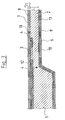
- the semiconductor component represented by the figures is provided for a sensor in the form of a pressure sensor or differential pressure sensor. It consists of a semiconductor substrate 1 of silicon, which is thinned out into a membrane 2 in a middle region. Semiconductor components in the form of resistors 3 are formed in the region of the membrane 2 by doping within the substrate 1 . The resistors 3 are connected via strip conductors 4 in a manner known per se to a bridge circuit.
- the strip conductors 4 are likewise formed within the semiconductor substrate 1 by doping with boron and led to wiring carriers 5 , so-called bond-pads, which are electrically connected to the strip conductors 4 and mechanically connected to the semiconductor substrate 1 and form the electrical connections of the semiconductor component, to which the electrical wiring is later effected by bonding.
- Such a semiconductor component as is schematically represented by FIGS. 1 and 2 , is clamped and sealed in the region which is delimited in FIG. 2 by the dotted lines 6 and 7 and which lies outside the membrane 2 , as well as next to the wiring carriers 5 , in a manner such that the membrane region may be reached by the medium, whose pressure or differential pressure is to be detected, and may be impinged on one side or both sides, without the wiring carriers 5 coming into contact with the medium.
- Metal-containing protective layers 8 and 9 are provided at both sides, in order to protect the region of the semiconductor substrate 1 , which comes into contact with the medium, in particular the membrane 2 , from corrosion and other undesirable influences caused by the medium.
- the substrate 1 is provided on both sides with a silicon oxide layer 10 which extends in a flat manner over the semiconductor substrate 1 on both sides, and is only interrupted in the region of the electrical connection of the wiring carrier 5 to the boron-doped region 4 , which lies within the semiconductor substrate 1 , as is evident from FIG. 4 .
- These silicon oxide layers 10 which are deposited on both sides have a thickness c of about 500 nm on the front side (this is the upper side in the FIGS. 1 , 3 and 4 ), thus where the wiring carriers 5 are also attached, whereas the silicon oxide layer 10 on the rear side or lower side has a thickness c of only 350 nm.
- the silicon oxide layer 10 is provided with a protective layer in the form of an amorphous tantalum oxide layer 8 which has a layer thickness of about 500 nm.
- This tantalum oxide layer 8 forms an anticorrosive protective layer for the region of the semiconductor substrate 1 which is located therebelow, and on the other hand, also forms an adhesive layer for the amorphous chromium-tantalum layer 9 , which is deposited thereabove and which likewise forms a protective layer.
- the layer thickness b of the chromium tantalum layer is about 800 nm.
- a multitude of such semiconductor components in the form of a wafer are manufactured together in a manner known per se, wherein the layers are manufactured in a successive manner by vapor deposition, and after completion of all layers, the wafer is mechanically divided up into individual components.
- the silicon oxide layers 10 After vapor deposition of the silicon oxide layers 10 , first the tantalum oxide layer 8 is vapor-deposited on the front side, as well as subsequently the chromium-tantalum layer 9 , whereafter the vapor deposition of the layers is effected on the rear side.
- a tantalum layer 11 is deposited on the silicon oxide layer 10 , before the deposition of the tantalum oxide layer 8 and the chromium tantalum layer 9 on the rear side.
- This tantalum layer 11 has a layer thickness d of 15 nm, thus is extremely thin, and then a tantalum oxide layer 8 and a chromium-tantalum layer 9 are vapor-deposited thereon, as with the front side.
- These layers too are amorphous and, as with the protective layers on the front side, are not formed up to the edge of the substrate 1 , but end at a distance therefrom.
- the region 12 in which the membrane 2 merges into the remaining, non-thinned region of the substrate 1 is designed in a rounded manner in the transition region. This transition region is indicated at 12 in FIG. 3 .
- the amorphous protective layers 8 and 9 may be induced with internal stress, induced by a suitable influencing of the parameters on vapor deposition, on one or both sides of the layers 8 , 9 , as well as on the front side and/or rear side, depending on the application case.
- internal stresses of about 500 MPa are induced in the outer layer 9 and of about 100 MPa in the inner layer 8 , and specifically in the form of compressive stresses.
- the thickness of the substrate is approx. 600 ⁇ m, and in the thinned-out membrane region 2 the thickness f is about 20 ⁇ m.
- the layer thicknesses of the metal-containing amorphous protective layers 8 and 9 on the rear side of the substrate 1 are about 30% greater than those of the corresponding layers 8 , 9 on the front side, as are specified above in detail.
Landscapes
- Chemical & Material Sciences (AREA)
- Analytical Chemistry (AREA)
- Physics & Mathematics (AREA)
- General Physics & Mathematics (AREA)
- Measuring Fluid Pressure (AREA)
- Pressure Sensors (AREA)
- Semiconductor Integrated Circuits (AREA)
- Mechanical Treatment Of Semiconductor (AREA)
- Bipolar Transistors (AREA)
- Noodles (AREA)
Abstract
Description
Claims (19)
Applications Claiming Priority (4)
| Application Number | Priority Date | Filing Date | Title |
|---|---|---|---|
| EP06019996.5 | 2006-09-25 | ||
| EP06019996 | 2006-09-25 | ||
| EP06019996A EP1903321B1 (en) | 2006-09-25 | 2006-09-25 | Semiconductor device |
| PCT/EP2007/007697 WO2008037334A1 (en) | 2006-09-25 | 2007-09-04 | Semiconductor component |
Publications (2)
| Publication Number | Publication Date |
|---|---|
| US20100044810A1 US20100044810A1 (en) | 2010-02-25 |
| US8294237B2 true US8294237B2 (en) | 2012-10-23 |
Family
ID=37728275
Family Applications (1)
| Application Number | Title | Priority Date | Filing Date |
|---|---|---|---|
| US12/442,738 Expired - Fee Related US8294237B2 (en) | 2006-09-25 | 2007-09-04 | Semiconductor structural element |
Country Status (6)
| Country | Link |
|---|---|
| US (1) | US8294237B2 (en) |
| EP (1) | EP1903321B1 (en) |
| CN (1) | CN101573601B (en) |
| AT (1) | ATE498831T1 (en) |
| DE (1) | DE502006008914D1 (en) |
| WO (1) | WO2008037334A1 (en) |
Cited By (1)
| Publication number | Priority date | Publication date | Assignee | Title |
|---|---|---|---|---|
| US9759623B2 (en) | 2012-11-28 | 2017-09-12 | Endress+Hauser Gmbh+Co. Kg | Pressure measuring cell |
Families Citing this family (4)
| Publication number | Priority date | Publication date | Assignee | Title |
|---|---|---|---|---|
| KR20100074568A (en) * | 2008-12-24 | 2010-07-02 | 삼성전자주식회사 | Host apparatus connected to image forming apparatus and web page printing method thereof |
| KR20110065015A (en) * | 2009-12-09 | 2011-06-15 | 삼성전자주식회사 | Bearing housing for washing machine and manufacturing method |
| CN103063339A (en) * | 2011-10-20 | 2013-04-24 | 刘胜 | Silicon piezoresistive type pressure sensor chip with shielding layer |
| GB2537984B (en) * | 2013-10-28 | 2019-02-27 | Inficon Gmbh | A method for preventing gases and fluids to penetrate a surface of an object |
Citations (9)
| Publication number | Priority date | Publication date | Assignee | Title |
|---|---|---|---|---|
| EP0736757A1 (en) | 1995-04-03 | 1996-10-09 | Motorola, Inc. | Media compatible microsensor structure by inorganic protection coating |
| EP0801150A2 (en) | 1996-04-12 | 1997-10-15 | Grundfos A/S | Electronic component |
| DE19842105A1 (en) | 1998-09-15 | 2000-03-16 | Bosch Gmbh Robert | Silicon masking layer system, for producing porous silicon structures useful in optics, chemical sensors and surface micromechanical structures, comprises a silicon dioxide layer, a bond layer and a protective layer |
| EP1217095A1 (en) | 2000-12-23 | 2002-06-26 | ALSTOM Power N.V. | Protective coating for an article used at high temperatures, particularly turbine components |
| DE29724622U1 (en) | 1996-04-12 | 2002-07-25 | Grundfos A/S, Bjerringbro | Electronic component |
| US20030199139A1 (en) * | 2002-04-23 | 2003-10-23 | Kee Jeung Lee | Capacitor in semiconductor device having dual dielectric film structure and method for fabricating the same |
| US20040113235A1 (en) * | 2002-12-13 | 2004-06-17 | International Business Machines Corporation | Damascene integration scheme for developing metal-insulator-metal capacitors |
| US20050280069A1 (en) * | 2004-06-21 | 2005-12-22 | Ichiro Mizushima | Semiconductor device and method of manufacturing the same |
| US20060219259A1 (en) * | 2005-04-04 | 2006-10-05 | Hynix Semiconductor Inc. | Method of cleaning a semiconductor wafer |
-
2006
- 2006-09-25 EP EP06019996A patent/EP1903321B1/en not_active Not-in-force
- 2006-09-25 AT AT06019996T patent/ATE498831T1/en active
- 2006-09-25 DE DE502006008914T patent/DE502006008914D1/en active Active
-
2007
- 2007-09-04 CN CN2007800355295A patent/CN101573601B/en not_active Expired - Fee Related
- 2007-09-04 WO PCT/EP2007/007697 patent/WO2008037334A1/en active Application Filing
- 2007-09-04 US US12/442,738 patent/US8294237B2/en not_active Expired - Fee Related
Patent Citations (11)
| Publication number | Priority date | Publication date | Assignee | Title |
|---|---|---|---|---|
| EP0736757A1 (en) | 1995-04-03 | 1996-10-09 | Motorola, Inc. | Media compatible microsensor structure by inorganic protection coating |
| EP0801150A2 (en) | 1996-04-12 | 1997-10-15 | Grundfos A/S | Electronic component |
| US6030709A (en) | 1996-04-12 | 2000-02-29 | Grundfos A/S | Electronic component |
| DE29724622U1 (en) | 1996-04-12 | 2002-07-25 | Grundfos A/S, Bjerringbro | Electronic component |
| DE19842105A1 (en) | 1998-09-15 | 2000-03-16 | Bosch Gmbh Robert | Silicon masking layer system, for producing porous silicon structures useful in optics, chemical sensors and surface micromechanical structures, comprises a silicon dioxide layer, a bond layer and a protective layer |
| EP1217095A1 (en) | 2000-12-23 | 2002-06-26 | ALSTOM Power N.V. | Protective coating for an article used at high temperatures, particularly turbine components |
| US20020132131A1 (en) | 2000-12-23 | 2002-09-19 | Hans-Peter Bossmann | Protective coating for a thermally stressed component, particularly a turbine component |
| US20030199139A1 (en) * | 2002-04-23 | 2003-10-23 | Kee Jeung Lee | Capacitor in semiconductor device having dual dielectric film structure and method for fabricating the same |
| US20040113235A1 (en) * | 2002-12-13 | 2004-06-17 | International Business Machines Corporation | Damascene integration scheme for developing metal-insulator-metal capacitors |
| US20050280069A1 (en) * | 2004-06-21 | 2005-12-22 | Ichiro Mizushima | Semiconductor device and method of manufacturing the same |
| US20060219259A1 (en) * | 2005-04-04 | 2006-10-05 | Hynix Semiconductor Inc. | Method of cleaning a semiconductor wafer |
Non-Patent Citations (1)
| Title |
|---|
| English translation of Written Opinion of the International Searching Authority issued on Nov. 12, 2007 in counterpart International Application No. PCT/EP2007/007697. |
Cited By (1)
| Publication number | Priority date | Publication date | Assignee | Title |
|---|---|---|---|---|
| US9759623B2 (en) | 2012-11-28 | 2017-09-12 | Endress+Hauser Gmbh+Co. Kg | Pressure measuring cell |
Also Published As
| Publication number | Publication date |
|---|---|
| DE502006008914D1 (en) | 2011-03-31 |
| EP1903321B1 (en) | 2011-02-16 |
| US20100044810A1 (en) | 2010-02-25 |
| EP1903321A1 (en) | 2008-03-26 |
| CN101573601B (en) | 2011-05-25 |
| ATE498831T1 (en) | 2011-03-15 |
| WO2008037334A1 (en) | 2008-04-03 |
| CN101573601A (en) | 2009-11-04 |
Similar Documents
| Publication | Publication Date | Title |
|---|---|---|
| EP3702722B1 (en) | Strain gauge and sensor module | |
| EP3690386B1 (en) | Strain gauge | |
| US8294237B2 (en) | Semiconductor structural element | |
| JP6018903B2 (en) | Physical quantity sensor | |
| US6507112B1 (en) | Semiconductor device with an improved bonding pad structure and method of bonding bonding wires to bonding pads | |
| US7081680B2 (en) | Self-aligned corrosion stop for copper C4 and wirebond | |
| US20110089505A1 (en) | Method for manufacturing a sensor component without passivation, and a sensor component | |
| US20080276713A1 (en) | Pressure sensor package and electronic part | |
| US11448560B2 (en) | Strain gauge and sensor module | |
| JP2018032846A (en) | Semiconductor sensor assembly for harsh media applications | |
| EP4261494A1 (en) | Strain gauge | |
| KR101072436B1 (en) | Pressure sensor having metal thin film type strain gauge | |
| US5703287A (en) | Measuring element for a flow sensor | |
| US6056888A (en) | Electronic component and method of manufacture | |
| EP1760442A2 (en) | Metal contact systems for semiconductor-based pressure sensors exposed to harsh chemical and thermal environments | |
| JP2022014344A (en) | Laminated electrodes, strain resistance membranes with electrodes and pressure sensors | |
| US7632759B2 (en) | Semiconductor device with front side metallization and method for the production thereof | |
| JPWO2004059722A1 (en) | Semiconductor sensor and plating method for semiconductor device | |
| JP2021039055A (en) | Sensor module and strain detection device | |
| US8299549B2 (en) | Layer structure for electrical contacting of semiconductor components | |
| JP5157654B2 (en) | Manufacturing method of semiconductor device | |
| CN117629498A (en) | Sensor component | |
| US20240369429A1 (en) | Strain gauge | |
| CN116659558A (en) | Metal member with insulating film, physical quantity sensor, and pressure sensor | |
| JP4978294B2 (en) | Semiconductor device and manufacturing method thereof |
Legal Events
| Date | Code | Title | Description |
|---|---|---|---|
| AS | Assignment |
Owner name: GRUNDFOS MANAGEMENT A/S,DENMARK Free format text: ASSIGNMENT OF ASSIGNORS INTEREST;ASSIGNORS:ERIKSEN, GERT FRIIS;DE REUS, ROGER;CHRISTENSEN, CARSTEN;REEL/FRAME:022446/0860 Effective date: 20090320 Owner name: GRUNDFOS MANAGEMENT A/S, DENMARK Free format text: ASSIGNMENT OF ASSIGNORS INTEREST;ASSIGNORS:ERIKSEN, GERT FRIIS;DE REUS, ROGER;CHRISTENSEN, CARSTEN;REEL/FRAME:022446/0860 Effective date: 20090320 |
|
| ZAAA | Notice of allowance and fees due |
Free format text: ORIGINAL CODE: NOA |
|
| ZAAB | Notice of allowance mailed |
Free format text: ORIGINAL CODE: MN/=. |
|
| STCF | Information on status: patent grant |
Free format text: PATENTED CASE |
|
| FPAY | Fee payment |
Year of fee payment: 4 |
|
| MAFP | Maintenance fee payment |
Free format text: PAYMENT OF MAINTENANCE FEE, 8TH YEAR, LARGE ENTITY (ORIGINAL EVENT CODE: M1552); ENTITY STATUS OF PATENT OWNER: LARGE ENTITY Year of fee payment: 8 |
|
| FEPP | Fee payment procedure |
Free format text: MAINTENANCE FEE REMINDER MAILED (ORIGINAL EVENT CODE: REM.); ENTITY STATUS OF PATENT OWNER: LARGE ENTITY |
|
| LAPS | Lapse for failure to pay maintenance fees |
Free format text: PATENT EXPIRED FOR FAILURE TO PAY MAINTENANCE FEES (ORIGINAL EVENT CODE: EXP.); ENTITY STATUS OF PATENT OWNER: LARGE ENTITY |
|
| STCH | Information on status: patent discontinuation |
Free format text: PATENT EXPIRED DUE TO NONPAYMENT OF MAINTENANCE FEES UNDER 37 CFR 1.362 |
|
| FP | Lapsed due to failure to pay maintenance fee |
Effective date: 20241023 |