EP4318562A1 - Power semiconductor device - Google Patents
Power semiconductor device Download PDFInfo
- Publication number
- EP4318562A1 EP4318562A1 EP21935030.3A EP21935030A EP4318562A1 EP 4318562 A1 EP4318562 A1 EP 4318562A1 EP 21935030 A EP21935030 A EP 21935030A EP 4318562 A1 EP4318562 A1 EP 4318562A1
- Authority
- EP
- European Patent Office
- Prior art keywords
- power semiconductor
- semiconductor device
- sealing resin
- conductive material
- transfer mold
- Prior art date
- Legal status (The legal status is an assumption and is not a legal conclusion. Google has not performed a legal analysis and makes no representation as to the accuracy of the status listed.)
- Pending
Links
Images


Classifications
-
- H—ELECTRICITY
- H10—SEMICONDUCTOR DEVICES; ELECTRIC SOLID-STATE DEVICES NOT OTHERWISE PROVIDED FOR
- H10W—GENERIC PACKAGES, INTERCONNECTIONS, CONNECTORS OR OTHER CONSTRUCTIONAL DETAILS OF DEVICES COVERED BY CLASS H10
- H10W40/00—Arrangements for thermal protection or thermal control
- H10W40/20—Arrangements for cooling
- H10W40/25—Arrangements for cooling characterised by their materials
- H10W40/255—Arrangements for cooling characterised by their materials having a laminate or multilayered structure, e.g. direct bond copper [DBC] ceramic substrates
-
- H—ELECTRICITY
- H10—SEMICONDUCTOR DEVICES; ELECTRIC SOLID-STATE DEVICES NOT OTHERWISE PROVIDED FOR
- H10W—GENERIC PACKAGES, INTERCONNECTIONS, CONNECTORS OR OTHER CONSTRUCTIONAL DETAILS OF DEVICES COVERED BY CLASS H10
- H10W42/00—Arrangements for protection of devices
- H10W42/20—Arrangements for protection of devices protecting against electromagnetic or particle radiation, e.g. light, X-rays, gamma-rays or electrons
-
- H—ELECTRICITY
- H10—SEMICONDUCTOR DEVICES; ELECTRIC SOLID-STATE DEVICES NOT OTHERWISE PROVIDED FOR
- H10W—GENERIC PACKAGES, INTERCONNECTIONS, CONNECTORS OR OTHER CONSTRUCTIONAL DETAILS OF DEVICES COVERED BY CLASS H10
- H10W42/00—Arrangements for protection of devices
- H10W42/20—Arrangements for protection of devices protecting against electromagnetic or particle radiation, e.g. light, X-rays, gamma-rays or electrons
- H10W42/25—Arrangements for protection of devices protecting against electromagnetic or particle radiation, e.g. light, X-rays, gamma-rays or electrons against alpha rays, e.g. for outer space applications
-
- H—ELECTRICITY
- H10—SEMICONDUCTOR DEVICES; ELECTRIC SOLID-STATE DEVICES NOT OTHERWISE PROVIDED FOR
- H10W—GENERIC PACKAGES, INTERCONNECTIONS, CONNECTORS OR OTHER CONSTRUCTIONAL DETAILS OF DEVICES COVERED BY CLASS H10
- H10W42/00—Arrangements for protection of devices
- H10W42/20—Arrangements for protection of devices protecting against electromagnetic or particle radiation, e.g. light, X-rays, gamma-rays or electrons
- H10W42/261—Arrangements for protection of devices protecting against electromagnetic or particle radiation, e.g. light, X-rays, gamma-rays or electrons characterised by their shapes or dispositions
- H10W42/276—Arrangements for protection of devices protecting against electromagnetic or particle radiation, e.g. light, X-rays, gamma-rays or electrons characterised by their shapes or dispositions the arrangements being on an external surface of the package, e.g. on the outer surface of an encapsulation
-
- H—ELECTRICITY
- H10—SEMICONDUCTOR DEVICES; ELECTRIC SOLID-STATE DEVICES NOT OTHERWISE PROVIDED FOR
- H10W—GENERIC PACKAGES, INTERCONNECTIONS, CONNECTORS OR OTHER CONSTRUCTIONAL DETAILS OF DEVICES COVERED BY CLASS H10
- H10W42/00—Arrangements for protection of devices
- H10W42/20—Arrangements for protection of devices protecting against electromagnetic or particle radiation, e.g. light, X-rays, gamma-rays or electrons
- H10W42/281—Arrangements for protection of devices protecting against electromagnetic or particle radiation, e.g. light, X-rays, gamma-rays or electrons characterised by their materials
- H10W42/284—Arrangements for protection of devices protecting against electromagnetic or particle radiation, e.g. light, X-rays, gamma-rays or electrons characterised by their materials shielding resins
-
- H—ELECTRICITY
- H10—SEMICONDUCTOR DEVICES; ELECTRIC SOLID-STATE DEVICES NOT OTHERWISE PROVIDED FOR
- H10W—GENERIC PACKAGES, INTERCONNECTIONS, CONNECTORS OR OTHER CONSTRUCTIONAL DETAILS OF DEVICES COVERED BY CLASS H10
- H10W42/00—Arrangements for protection of devices
- H10W42/60—Arrangements for protection of devices protecting against electrostatic charges or discharges, e.g. Faraday shields
-
- H—ELECTRICITY
- H10—SEMICONDUCTOR DEVICES; ELECTRIC SOLID-STATE DEVICES NOT OTHERWISE PROVIDED FOR
- H10W—GENERIC PACKAGES, INTERCONNECTIONS, CONNECTORS OR OTHER CONSTRUCTIONAL DETAILS OF DEVICES COVERED BY CLASS H10
- H10W70/00—Package substrates; Interposers; Redistribution layers [RDL]
- H10W70/40—Leadframes
- H10W70/481—Leadframes for devices being provided for in groups H10D8/00 - H10D48/00
-
- H—ELECTRICITY
- H10—SEMICONDUCTOR DEVICES; ELECTRIC SOLID-STATE DEVICES NOT OTHERWISE PROVIDED FOR
- H10W—GENERIC PACKAGES, INTERCONNECTIONS, CONNECTORS OR OTHER CONSTRUCTIONAL DETAILS OF DEVICES COVERED BY CLASS H10
- H10W74/00—Encapsulations, e.g. protective coatings
- H10W74/10—Encapsulations, e.g. protective coatings characterised by their shape or disposition
-
- H—ELECTRICITY
- H10—SEMICONDUCTOR DEVICES; ELECTRIC SOLID-STATE DEVICES NOT OTHERWISE PROVIDED FOR
- H10W—GENERIC PACKAGES, INTERCONNECTIONS, CONNECTORS OR OTHER CONSTRUCTIONAL DETAILS OF DEVICES COVERED BY CLASS H10
- H10W74/00—Encapsulations, e.g. protective coatings
- H10W74/10—Encapsulations, e.g. protective coatings characterised by their shape or disposition
- H10W74/111—Encapsulations, e.g. protective coatings characterised by their shape or disposition the semiconductor body being completely enclosed
-
- H—ELECTRICITY
- H10—SEMICONDUCTOR DEVICES; ELECTRIC SOLID-STATE DEVICES NOT OTHERWISE PROVIDED FOR
- H10W—GENERIC PACKAGES, INTERCONNECTIONS, CONNECTORS OR OTHER CONSTRUCTIONAL DETAILS OF DEVICES COVERED BY CLASS H10
- H10W74/00—Encapsulations, e.g. protective coatings
- H10W74/10—Encapsulations, e.g. protective coatings characterised by their shape or disposition
- H10W74/111—Encapsulations, e.g. protective coatings characterised by their shape or disposition the semiconductor body being completely enclosed
- H10W74/121—Encapsulations, e.g. protective coatings characterised by their shape or disposition the semiconductor body being completely enclosed by multiple encapsulations, e.g. by a thin protective coating and a thick encapsulation
-
- H—ELECTRICITY
- H10—SEMICONDUCTOR DEVICES; ELECTRIC SOLID-STATE DEVICES NOT OTHERWISE PROVIDED FOR
- H10W—GENERIC PACKAGES, INTERCONNECTIONS, CONNECTORS OR OTHER CONSTRUCTIONAL DETAILS OF DEVICES COVERED BY CLASS H10
- H10W74/00—Encapsulations, e.g. protective coatings
- H10W74/40—Encapsulations, e.g. protective coatings characterised by their materials
- H10W74/47—Encapsulations, e.g. protective coatings characterised by their materials comprising organic materials, e.g. plastics or resins
- H10W74/473—Encapsulations, e.g. protective coatings characterised by their materials comprising organic materials, e.g. plastics or resins containing a filler
-
- H—ELECTRICITY
- H10—SEMICONDUCTOR DEVICES; ELECTRIC SOLID-STATE DEVICES NOT OTHERWISE PROVIDED FOR
- H10W—GENERIC PACKAGES, INTERCONNECTIONS, CONNECTORS OR OTHER CONSTRUCTIONAL DETAILS OF DEVICES COVERED BY CLASS H10
- H10W76/00—Containers; Fillings or auxiliary members therefor; Seals
- H10W76/10—Containers or parts thereof
- H10W76/12—Containers or parts thereof characterised by their shape
- H10W76/13—Containers comprising a conductive base serving as an interconnection
-
- H—ELECTRICITY
- H10—SEMICONDUCTOR DEVICES; ELECTRIC SOLID-STATE DEVICES NOT OTHERWISE PROVIDED FOR
- H10W—GENERIC PACKAGES, INTERCONNECTIONS, CONNECTORS OR OTHER CONSTRUCTIONAL DETAILS OF DEVICES COVERED BY CLASS H10
- H10W76/00—Containers; Fillings or auxiliary members therefor; Seals
- H10W76/10—Containers or parts thereof
- H10W76/12—Containers or parts thereof characterised by their shape
- H10W76/15—Containers comprising an insulating or insulated base
-
- H—ELECTRICITY
- H10—SEMICONDUCTOR DEVICES; ELECTRIC SOLID-STATE DEVICES NOT OTHERWISE PROVIDED FOR
- H10W—GENERIC PACKAGES, INTERCONNECTIONS, CONNECTORS OR OTHER CONSTRUCTIONAL DETAILS OF DEVICES COVERED BY CLASS H10
- H10W76/00—Containers; Fillings or auxiliary members therefor; Seals
- H10W76/10—Containers or parts thereof
- H10W76/17—Containers or parts thereof characterised by their materials
-
- H—ELECTRICITY
- H10—SEMICONDUCTOR DEVICES; ELECTRIC SOLID-STATE DEVICES NOT OTHERWISE PROVIDED FOR
- H10W—GENERIC PACKAGES, INTERCONNECTIONS, CONNECTORS OR OTHER CONSTRUCTIONAL DETAILS OF DEVICES COVERED BY CLASS H10
- H10W76/00—Containers; Fillings or auxiliary members therefor; Seals
- H10W76/40—Fillings or auxiliary members in containers, e.g. centering rings
- H10W76/42—Fillings
- H10W76/47—Solid or gel fillings
-
- H—ELECTRICITY
- H10—SEMICONDUCTOR DEVICES; ELECTRIC SOLID-STATE DEVICES NOT OTHERWISE PROVIDED FOR
- H10W—GENERIC PACKAGES, INTERCONNECTIONS, CONNECTORS OR OTHER CONSTRUCTIONAL DETAILS OF DEVICES COVERED BY CLASS H10
- H10W72/00—Interconnections or connectors in packages
- H10W72/50—Bond wires
-
- H—ELECTRICITY
- H10—SEMICONDUCTOR DEVICES; ELECTRIC SOLID-STATE DEVICES NOT OTHERWISE PROVIDED FOR
- H10W—GENERIC PACKAGES, INTERCONNECTIONS, CONNECTORS OR OTHER CONSTRUCTIONAL DETAILS OF DEVICES COVERED BY CLASS H10
- H10W72/00—Interconnections or connectors in packages
- H10W72/851—Dispositions of multiple connectors or interconnections
- H10W72/874—On different surfaces
- H10W72/884—Die-attach connectors and bond wires
-
- H—ELECTRICITY
- H10—SEMICONDUCTOR DEVICES; ELECTRIC SOLID-STATE DEVICES NOT OTHERWISE PROVIDED FOR
- H10W—GENERIC PACKAGES, INTERCONNECTIONS, CONNECTORS OR OTHER CONSTRUCTIONAL DETAILS OF DEVICES COVERED BY CLASS H10
- H10W74/00—Encapsulations, e.g. protective coatings
-
- H—ELECTRICITY
- H10—SEMICONDUCTOR DEVICES; ELECTRIC SOLID-STATE DEVICES NOT OTHERWISE PROVIDED FOR
- H10W—GENERIC PACKAGES, INTERCONNECTIONS, CONNECTORS OR OTHER CONSTRUCTIONAL DETAILS OF DEVICES COVERED BY CLASS H10
- H10W90/00—Package configurations
- H10W90/701—Package configurations characterised by the relative positions of pads or connectors relative to package parts
- H10W90/731—Package configurations characterised by the relative positions of pads or connectors relative to package parts of die-attach connectors
- H10W90/734—Package configurations characterised by the relative positions of pads or connectors relative to package parts of die-attach connectors between a chip and a stacked insulating package substrate, interposer or RDL
-
- H—ELECTRICITY
- H10—SEMICONDUCTOR DEVICES; ELECTRIC SOLID-STATE DEVICES NOT OTHERWISE PROVIDED FOR
- H10W—GENERIC PACKAGES, INTERCONNECTIONS, CONNECTORS OR OTHER CONSTRUCTIONAL DETAILS OF DEVICES COVERED BY CLASS H10
- H10W90/00—Package configurations
- H10W90/701—Package configurations characterised by the relative positions of pads or connectors relative to package parts
- H10W90/731—Package configurations characterised by the relative positions of pads or connectors relative to package parts of die-attach connectors
- H10W90/736—Package configurations characterised by the relative positions of pads or connectors relative to package parts of die-attach connectors between a chip and a stacked lead frame, conducting package substrate or heat sink
-
- H—ELECTRICITY
- H10—SEMICONDUCTOR DEVICES; ELECTRIC SOLID-STATE DEVICES NOT OTHERWISE PROVIDED FOR
- H10W—GENERIC PACKAGES, INTERCONNECTIONS, CONNECTORS OR OTHER CONSTRUCTIONAL DETAILS OF DEVICES COVERED BY CLASS H10
- H10W90/00—Package configurations
- H10W90/701—Package configurations characterised by the relative positions of pads or connectors relative to package parts
- H10W90/751—Package configurations characterised by the relative positions of pads or connectors relative to package parts of bond wires
- H10W90/754—Package configurations characterised by the relative positions of pads or connectors relative to package parts of bond wires between a chip and a stacked insulating package substrate, interposer or RDL
-
- H—ELECTRICITY
- H10—SEMICONDUCTOR DEVICES; ELECTRIC SOLID-STATE DEVICES NOT OTHERWISE PROVIDED FOR
- H10W—GENERIC PACKAGES, INTERCONNECTIONS, CONNECTORS OR OTHER CONSTRUCTIONAL DETAILS OF DEVICES COVERED BY CLASS H10
- H10W90/00—Package configurations
- H10W90/701—Package configurations characterised by the relative positions of pads or connectors relative to package parts
- H10W90/751—Package configurations characterised by the relative positions of pads or connectors relative to package parts of bond wires
- H10W90/756—Package configurations characterised by the relative positions of pads or connectors relative to package parts of bond wires between a chip and a stacked lead frame, conducting package substrate or heat sink
Definitions
- the present disclosed invention relates to a power semiconductor device.
- space environment In high-altitude environments and space environments (hereinafter referred to as "space environment or the like"), a large amount of cosmic rays are falling. A semiconductor chip in a semiconductor device placed in a radiation environment such as a space environment malfunctions, and an insulating member deteriorates.
- Patent Literature 1 a radiation resistant package implement by mixing or laminating heavy elements such as lead and tungsten into a plastic molding material
- Patent Literature 1 Japanese Patent Application Laid-Open JP Hei 1- 300 547 A
- a power semiconductor device for aircraft has a feature that a use voltage is larger than that of a semiconductor device for space use. Even when the package according to the related art is used in a power semiconductor device for an aircraft, since a use voltage is large, deterioration of insulation performance due to charging of cosmic rays is a problem.
- An object of the present disclosed invention is to solve the above problem and to provide a power semiconductor device in which dielectric breakdown does not occur in addition to reduction of malfunction of a semiconductor chip caused by cosmic rays.
- a power semiconductor according to the present disclosed invention is a case-type power semiconductor device, in which a case is formed by mixing a heavy element material and a conductive material with a material having high processability, the conductive material is not a light metal, and electric resistance of the case is 1.0 E5 to 1.0 E11 [ ⁇ ].
- the power semiconductor according to the present disclosed invention is a transfer mold-type power semiconductor device including a transfer mold-type sealing resin including a sealing resin containing a heavy element material and a sealing resin containing a conductive material, wherein the conductive material of the sealing resin containing a conductive material is not a light metal.
- the power semiconductor device according to the present disclosed invention has the above-described configuration, there is an effect that malfunction of a semiconductor chip generated by cosmic rays is reduced and dielectric breakdown is not caused.
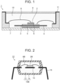
- FIG. 1 is a cross-sectional view illustrating a power semiconductor device (case type) 1 according to a first embodiment.
- a power semiconductor device (case type) 1 illustrated in FIG. 1 an insulating substrate 4 and a semiconductor chip 2 are covered with a potting type insulating sealing resin 10 using a case 9 as an enclosure.
- a case-type power semiconductor device (case type) 1 includes the semiconductor chip 2, an upper electrode 3, the insulating substrate 4, a lower electrode 5, a solder 6, a base plate 7, a wire 8, the case 9, the sealing resin 10, and an external terminal 11.
- the case 9 is formed by mixing a heavy element material and a conductive material with a material having high processability.
- the material having high processability may be, for example, a thermosetting resin or the like.
- the heavy element material intended by the present disclosed invention is a heavy metal represented by W or Pb, or a compound with a heavy metal such as tungsten oxide.
- the conductive material intended by the present disclosed invention is, for example, carbon black, carbon fiber, or a material equivalent thereto, and does not mean a light metal represented by Al.
- weight reduction is achieved.
- a more preferable condition is that the heavy element material and the carbon-based conductive material are mixed at a ratio such that the entire electric resistance value is from 1.0 E5 to 1.0 E11 [ ⁇ ].
- the lower electrode 5 is bonded onto the base plate 7 by the solder 6.
- the insulating substrate 4 and the upper electrode 3 are arranged in this order on the lower electrode 5.
- the upper electrode 3 and the lower electrode 5 are desirably formed of a metal having low electric resistance, such as copper or aluminum.
- the semiconductor chip 2 is bonded onto the upper electrode 3 by the solder 6.
- the semiconductor chip 2 and the external terminal 11 are electrically connected by the wire 8.
- a silver bonding material may be used instead of the solder 6.
- the solder 6 may be used for connection between the upper electrode 3 and the insulating substrate 4, or a silver bonding material may be used instead of the solder 6.
- the power semiconductor device (case type) 1 is surrounded by the case 9, and the inside of the case 9 is filled with the sealing resin 10.
- the base plate 7 is desirably formed of a metal having high thermal conductivity, such as copper or aluminum.
- the wire 8 is formed of metal having low electric resistance, such as copper or aluminum.
- the heavy element material mixed in the case 9 contributes to preventing the entrance of cosmic rays into the semiconductor chip 2.
- the conductive material mixed in the case 9 contributes to preventing the charging of cosmic rays.
- the conductive material mixed in the case 9 prevents local charging in the vicinity of the surface of the case 9 due to cosmic rays, and prevents dielectric breakdown occurring at the interface between the external terminal 11 and the case 9.
- the power semiconductor device (case type) 1 according to the first embodiment illustrated in FIG. 1 has the above-described configuration, radiation resistance and antistatic properties are imparted, and electrical insulation performance is improved. By this action, the power semiconductor device (case type) 1 according to the first embodiment has an effect of reducing malfunction of the semiconductor chip 2 caused by cosmic rays and not causing dielectric breakdown.
- a transfer mold-type package structure can also be implemented.
- the present disclosed invention can also be applied to a transfer mold-type package structure.
- FIG. 2 is a cross-sectional view illustrating a power semiconductor device (transfer mold type) 12 according to the first embodiment.
- the power semiconductor device (transfer mold type) 12 includes a semiconductor chip 2B, a wire 8B, a transfer mold-type sealing resin 10B including a sealing resin 13 containing a heavy element material and a sealing resin 14 containing a conductive material, a lead frame 15, and a lead terminal 16.
- the semiconductor chip 2B is mounted on the lead frame 15.
- the semiconductor chip 2B may be, for example, an element such as an IGBT or a MOSFET, and may include one element or a plurality of elements.
- the elements used may be of the same type or different types.
- the lead terminal 16 and the semiconductor chip 2B are electrically connected by the wire 8B.
- the transfer mold-type sealing resin 10B covering the power semiconductor device (transfer mold type) 12 has a two-layer structure, an inner layer is the sealing resin 13 containing a heavy element material, and an outer layer is the sealing resin 14 containing a conductive material.
- the sealing resin 13 containing a heavy element material absorbs radiation.
- the sealing resin 14 containing a conductive material prevents charging.
- the amount of cosmic rays entering the semiconductor chip 2B is reduced, and local charging in the vicinity of the surface of the transfer mold-type sealing resin 10B due to the cosmic rays is prevented.
- dielectric breakdown at the interface between the lead terminal 16 and the sealing resin 14 containing a conductive material is prevented.
- a second embodiment is an aspect in which, in the power semiconductor device (transfer mold type) 12 described in the first embodiment, a portion where dielectric breakdown is likely to occur is further devised.
- the same reference numerals as those in the first embodiment are used unless otherwise distinguished. Further, the description overlapping with the first embodiment is appropriately omitted.
- FIG. 3 is a cross-sectional view, a side view, and a bottom view illustrating a power semiconductor device (transfer mold type) 17 according to the second embodiment.
- the power semiconductor device (transfer mold type) 17 according to the second embodiment includes a barrier wall 18 on a surface of an outer layer of a sealing resin 14 containing a conductive material.
- a portion where dielectric breakdown is likely to occur can be specified.
- a portion where dielectric breakdown is likely to occur in FIG. 2 according to the first embodiment will be described.
- the portion is between the lead terminal 16 and another adjacent lead terminal 16, and is the surface of the sealing resin 14 containing a conductive material.
- barrier walls 18 are provided on the surface of the sealing resin 14 containing a conductive material in such a way as to partition the lead terminal 16 from another adjacent lead terminal 16.
- the barrier wall 18 increases a creepage distance between the lead terminal 16 and another adjacent lead terminal 16 to improve insulation performance.
- the power semiconductor device (transfer mold type) 17 according to the second embodiment has an effect of increasing the creepage distance between the lead terminal 16 and another adjacent lead terminal 16 and improving the insulation performance, in addition to the effects described in the first embodiment.
- the barrier wall 18 may be provided on the surface of the case 9 of the power semiconductor device (case type) 1 illustrated in FIG. 1 . Providing the barrier wall 18 has an effect of increasing the creepage distance and improving the insulation performance even in the power semiconductor device (case type) 1.
- a third embodiment is also an aspect in which the power semiconductor device (transfer mold type) 12 described in the first embodiment is further devised at a portion where dielectric breakdown is likely to occur.
- the same reference numerals as those used in the above-described embodiments are used unless otherwise specified. Further, the description overlapping with the above-described embodiments is appropriately omitted.
- FIG. 4 is a cross-sectional view, a side view, and a bottom view of a power semiconductor device (transfer mold type) 19 according to the third embodiment.
- the power semiconductor device (transfer mold type) 19 according to the third embodiment includes a wavy structure 20.
- the wavy structure 20 is obtained by literally waving the surface of the sealing resin 14 containing a conductive material.
- the wavy structure 20 increases the creepage distance between the lead terminal 16 and another adjacent lead terminal 16, and improves the insulation performance.
- the power semiconductor device (transfer mold type) 19 according to the third embodiment has an effect of increasing the creepage distance between the lead terminal 16 and another adjacent lead terminal 16 and improving the insulation performance, in addition to the effects described in the first embodiment.
- a fourth embodiment is an aspect in which antistatic properties are further devised in the power semiconductor device (transfer mold type) 12 (12, 17, 19) described in the previously described embodiments.
- the same reference numerals as those used in the above-described embodiments are used unless otherwise specified. Further, the description overlapping with the above-described embodiments is appropriately omitted.
- FIG. 5 is a cross-sectional view illustrating a power semiconductor device (transfer mold type) 21 according to the fourth embodiment. As illustrated in FIG. 5 , the power semiconductor device (transfer mold type) 21 according to the fourth embodiment includes a metal layer 22.
- the metal layer 22 is provided between the sealing resin 13 containing a heavy element material and the sealing resin 14 containing a conductive material. In addition, the metal layer 22 is grounded.
- the sealing resin 14 containing a conductive material disperses charges generated by cosmic rays and prevents local charging.
- electric field enhancement due to charging cannot be prevented only by the sealing resin 14 containing a conductive material.
- the metal layer 22 removes electric charge generated by cosmic rays and contributes to further improvement in electrification resistance.
- the power semiconductor device (transfer mold type) 21 according to the fourth embodiment has the effect of removing the charge generated by the cosmic ray because of the grounding of the metal layer 22 and further improving the electrification resistance, in addition to the effect described in the first embodiment.
- a fifth embodiment is an aspect in which an improvement in radiation resistance is devised in the power semiconductor device (transfer mold type) 12 (12, 17, 19, 21) described in the previously described embodiments.
- the same reference numerals as those used in the above-described embodiments are used unless otherwise specified. Further, the description overlapping with the above-described embodiments is appropriately omitted.
- FIG. 6 is a cross-sectional view illustrating a power semiconductor device (transfer mold type) 23 according to the fifth embodiment.
- the power semiconductor device (transfer mold type) 23 according to the fifth embodiment uses a mixed transfer mold resin 24 instead of the sealing resin 14 containing a conductive material.
- the mixed transfer mold resin 24 is a transfer mold resin in which a heavy element material and a conductive material are mixed.
- the mixed transfer mold resin 24 contains a heavy element material, cosmic rays are prevented from entering the package.
- the fact that the mixed transfer mold resin 24 contains the heavy element material means that the heavy element material is used more than the case of using only the sealing resin 13 containing the heavy element material, and the radiation resistance is improved.
- the power semiconductor device (transfer mold type) 23 according to the fifth embodiment has an effect of improving radiation resistance in addition to the effect described in the first embodiment.
- a sixth embodiment shows a modification in which a part of the configuration shown in the fifth embodiment is changed.
- the same reference numerals as those used in the above-described embodiments are used unless otherwise specified. Further, the description overlapping with the above-described embodiments is appropriately omitted.
- FIG. 7 is a cross-sectional view illustrating a power semiconductor device (transfer mold type) 25 according to the sixth embodiment.
- the power semiconductor device (transfer mold type) 25 according to the sixth embodiment uses a non-mixed transfer mold resin 26 instead of the sealing resin 13 containing a heavy element material.
- the non-mixed transfer mold resin 26 is a transfer mold resin in which a heavy element material is not mixed.
- the mixed transfer mold resin 24 contains a heavy element material, cosmic rays are prevented from entering the package. Therefore, when the mixed transfer mold resin 24 is used, radiation resistance can be ensured without using the sealing resin 13 containing a heavy element material.
- a heavy element material may be used in any layer, and a conductive material may be also used in any layer.
- the amount of cosmic rays entering the semiconductor chip 2B is reduced, and local charging in the vicinity of the surface of the transfer mold-type sealing resin 10C due to the cosmic rays is prevented.
- a seventh embodiment is an aspect in which improvement in radiation resistance is devised in the power semiconductor device (case type) 1 described in the first embodiment.
- the same reference numerals as those used in the above-described embodiments are used unless otherwise specified. Further, the description overlapping with the above-described embodiments is appropriately omitted.
- FIG. 8 is a cross-sectional view illustrating a power semiconductor device (case type) 27 according to the seventh embodiment.
- the power semiconductor device (case type) 27 according to the seventh embodiment uses a mixed sealing resin 28 instead of the sealing resin 10.
- the mixed sealing resin 28 is obtained by mixing a heavy element material with the sealing resin 10.
- the mixed sealing resin 28 contains a heavy element material, cosmic rays are prevented from entering the package.
- the fact that the mixed sealing resin 28 contains the heavy element material means that the heavy element material is used more than in the case of only the case 9 containing the heavy element material, and the radiation resistance is improved.
- the power semiconductor device (case type) 27 according to the seventh embodiment has an effect of improving radiation resistance in addition to the effect described in the first embodiment.
- the present disclosed invention can be applied to power semiconductors for aircraft applications and the like, and has industrial applicability.
Landscapes
- Structures Or Materials For Encapsulating Or Coating Semiconductor Devices Or Solid State Devices (AREA)
- Physics & Mathematics (AREA)
- Health & Medical Sciences (AREA)
- Electromagnetism (AREA)
- Toxicology (AREA)
Abstract
Description
- The present disclosed invention relates to a power semiconductor device.
- In high-altitude environments and space environments (hereinafter referred to as "space environment or the like"), a large amount of cosmic rays are falling. A semiconductor chip in a semiconductor device placed in a radiation environment such as a space environment malfunctions, and an insulating member deteriorates.
- Various techniques are disclosed for packaging semiconductor devices used in a radiation environment such as a space environment. For example, there is known a radiation resistant package implement by mixing or laminating heavy elements such as lead and tungsten into a plastic molding material (For example, Patent Literature 1).
- Patent Literature 1: Japanese Patent Application Laid-Open
JP Hei 1- 300 547 A - Meanwhile, since power semiconductor devices for aircraft are also used at high altitude, it is necessary to take measures so as not to be adversely affected by cosmic rays. A power semiconductor device for aircraft has a feature that a use voltage is larger than that of a semiconductor device for space use. Even when the package according to the related art is used in a power semiconductor device for an aircraft, since a use voltage is large, deterioration of insulation performance due to charging of cosmic rays is a problem.
- An object of the present disclosed invention is to solve the above problem and to provide a power semiconductor device in which dielectric breakdown does not occur in addition to reduction of malfunction of a semiconductor chip caused by cosmic rays.
- A power semiconductor according to the present disclosed invention is a case-type power semiconductor device, in which a case is formed by mixing a heavy element material and a conductive material with a material having high processability,
the conductive material is not a light metal, and electric resistance of the case is 1.0 E5 to 1.0 E11 [Ω]. - In addition, the power semiconductor according to the present disclosed invention is a transfer mold-type power semiconductor device including a transfer mold-type sealing resin including a sealing resin containing a heavy element material and a sealing resin containing a conductive material, wherein the conductive material of the sealing resin containing a conductive material is not a light metal.
- Since the power semiconductor device according to the present disclosed invention has the above-described configuration, there is an effect that malfunction of a semiconductor chip generated by cosmic rays is reduced and dielectric breakdown is not caused.
-
-
FIG. 1 is a cross-sectional view illustrating a case-type power semiconductor device (1) according to a first embodiment. -
FIG. 2 is a cross-sectional view illustrating a transfer mold-type power semiconductor device (12) according to the first embodiment. -
FIG. 3 is a cross-sectional view, a side view, and a bottom view illustrating a transfer mold-type power semiconductor device (17) according to a second embodiment. -
FIG. 4 is a cross-sectional view, a side view, and a bottom view of a transfer mold-type power semiconductor device (19) according to a third embodiment. -
FIG. 5 is a cross-sectional view illustrating a transfer mold-type power semiconductor device (21) according to a fourth embodiment. -
FIG. 6 is a cross-sectional view illustrating a transfer mold-type power semiconductor device (23) according to a fifth embodiment. -
FIG. 7 is a cross-sectional view illustrating a transfer mold-type power semiconductor device (25) according to a sixth embodiment. -
FIG. 8 is a cross-sectional view illustrating a case-type power semiconductor device (27) according to a seventh embodiment. -
FIG. 1 is a cross-sectional view illustrating a power semiconductor device (case type) 1 according to a first embodiment. In a power semiconductor device (case type) 1 illustrated inFIG. 1 , aninsulating substrate 4 and asemiconductor chip 2 are covered with a potting type insulatingsealing resin 10 using acase 9 as an enclosure. - As illustrated in
FIG. 1 , a case-type power semiconductor device (case type) 1 according to the first embodiment includes thesemiconductor chip 2, anupper electrode 3, theinsulating substrate 4, alower electrode 5, asolder 6, abase plate 7, awire 8, thecase 9, thesealing resin 10, and anexternal terminal 11. - The
case 9 is formed by mixing a heavy element material and a conductive material with a material having high processability. The material having high processability may be, for example, a thermosetting resin or the like. Here, the heavy element material intended by the present disclosed invention is a heavy metal represented by W or Pb, or a compound with a heavy metal such as tungsten oxide. - In addition, the conductive material intended by the present disclosed invention is, for example, carbon black, carbon fiber, or a material equivalent thereto, and does not mean a light metal represented by Al. By not using a light metal for the conductive material, weight reduction is achieved. A more preferable condition is that the heavy element material and the carbon-based conductive material are mixed at a ratio such that the entire electric resistance value is from 1.0 E5 to 1.0 E11 [Ω].
- The
lower electrode 5 is bonded onto thebase plate 7 by thesolder 6. Theinsulating substrate 4 and theupper electrode 3 are arranged in this order on thelower electrode 5. Theupper electrode 3 and thelower electrode 5 are desirably formed of a metal having low electric resistance, such as copper or aluminum. - The
semiconductor chip 2 is bonded onto theupper electrode 3 by thesolder 6. Thesemiconductor chip 2 and theexternal terminal 11 are electrically connected by thewire 8. For connection of thesemiconductor chip 2 to theupper electrode 3, a silver bonding material may be used instead of thesolder 6. Similarly, thesolder 6 may be used for connection between theupper electrode 3 and theinsulating substrate 4, or a silver bonding material may be used instead of thesolder 6. - The power semiconductor device (case type) 1 is surrounded by the
case 9, and the inside of thecase 9 is filled with the sealingresin 10. - The
base plate 7 is desirably formed of a metal having high thermal conductivity, such as copper or aluminum. - It is desirable that the
wire 8 is formed of metal having low electric resistance, such as copper or aluminum. - The heavy element material mixed in the
case 9 contributes to preventing the entrance of cosmic rays into thesemiconductor chip 2. The conductive material mixed in thecase 9 contributes to preventing the charging of cosmic rays. - More specifically, the conductive material mixed in the
case 9 prevents local charging in the vicinity of the surface of thecase 9 due to cosmic rays, and prevents dielectric breakdown occurring at the interface between theexternal terminal 11 and thecase 9. - Since the power semiconductor device (case type) 1 according to the first embodiment illustrated in
FIG. 1 has the above-described configuration, radiation resistance and antistatic properties are imparted, and electrical insulation performance is improved. By this action, the power semiconductor device (case type) 1 according to the first embodiment has an effect of reducing malfunction of thesemiconductor chip 2 caused by cosmic rays and not causing dielectric breakdown. - With development of a direct lead bonding (DLB) invention, a transfer mold-type package structure can also be implemented. The present disclosed invention can also be applied to a transfer mold-type package structure.
-
FIG. 2 is a cross-sectional view illustrating a power semiconductor device (transfer mold type) 12 according to the first embodiment. As illustrated inFIG. 2 , the power semiconductor device (transfer mold type) 12 includes asemiconductor chip 2B, awire 8B, a transfer mold-type sealing resin 10B including asealing resin 13 containing a heavy element material and asealing resin 14 containing a conductive material, alead frame 15, and alead terminal 16. - The
semiconductor chip 2B is mounted on thelead frame 15. Note that thesemiconductor chip 2B may be, for example, an element such as an IGBT or a MOSFET, and may include one element or a plurality of elements. When thesemiconductor chip 2B includes a plurality of elements, the elements used may be of the same type or different types. - The
lead terminal 16 and thesemiconductor chip 2B are electrically connected by thewire 8B. - The transfer mold-
type sealing resin 10B covering the power semiconductor device (transfer mold type) 12 has a two-layer structure, an inner layer is the sealingresin 13 containing a heavy element material, and an outer layer is the sealingresin 14 containing a conductive material. The sealingresin 13 containing a heavy element material absorbs radiation. The sealingresin 14 containing a conductive material prevents charging. - With the above configuration, in the power semiconductor device (transfer mold type) 12 according to the first embodiment, the amount of cosmic rays entering the
semiconductor chip 2B is reduced, and local charging in the vicinity of the surface of the transfer mold-type sealing resin 10B due to the cosmic rays is prevented. In addition, in the power semiconductor device (transfer mold type) 12, dielectric breakdown at the interface between thelead terminal 16 and the sealingresin 14 containing a conductive material is prevented. - A second embodiment is an aspect in which, in the power semiconductor device (transfer mold type) 12 described in the first embodiment, a portion where dielectric breakdown is likely to occur is further devised. In the second embodiment, the same reference numerals as those in the first embodiment are used unless otherwise distinguished. Further, the description overlapping with the first embodiment is appropriately omitted.
-
FIG. 3 is a cross-sectional view, a side view, and a bottom view illustrating a power semiconductor device (transfer mold type) 17 according to the second embodiment. As shown inFIG. 3 , the power semiconductor device (transfer mold type) 17 according to the second embodiment includes abarrier wall 18 on a surface of an outer layer of a sealingresin 14 containing a conductive material. - In general, in a transfer mold-type semiconductor device, a portion where dielectric breakdown is likely to occur can be specified. A portion where dielectric breakdown is likely to occur in
FIG. 2 according to the first embodiment will be described. The portion is between thelead terminal 16 and anotheradjacent lead terminal 16, and is the surface of the sealingresin 14 containing a conductive material. - As shown in
FIG. 3 , a required number ofbarrier walls 18 are provided on the surface of the sealingresin 14 containing a conductive material in such a way as to partition thelead terminal 16 from anotheradjacent lead terminal 16. Thebarrier wall 18 increases a creepage distance between thelead terminal 16 and anotheradjacent lead terminal 16 to improve insulation performance. - With the above configuration, the power semiconductor device (transfer mold type) 17 according to the second embodiment has an effect of increasing the creepage distance between the
lead terminal 16 and anotheradjacent lead terminal 16 and improving the insulation performance, in addition to the effects described in the first embodiment. - Note that the
barrier wall 18 may be provided on the surface of thecase 9 of the power semiconductor device (case type) 1 illustrated inFIG. 1 . Providing thebarrier wall 18 has an effect of increasing the creepage distance and improving the insulation performance even in the power semiconductor device (case type) 1. - A third embodiment is also an aspect in which the power semiconductor device (transfer mold type) 12 described in the first embodiment is further devised at a portion where dielectric breakdown is likely to occur. In the third embodiment, the same reference numerals as those used in the above-described embodiments are used unless otherwise specified. Further, the description overlapping with the above-described embodiments is appropriately omitted.
-
FIG. 4 is a cross-sectional view, a side view, and a bottom view of a power semiconductor device (transfer mold type) 19 according to the third embodiment. As illustrated inFIG. 4 , the power semiconductor device (transfer mold type) 19 according to the third embodiment includes awavy structure 20. - The
wavy structure 20 is obtained by literally waving the surface of the sealingresin 14 containing a conductive material. Thewavy structure 20 increases the creepage distance between thelead terminal 16 and anotheradjacent lead terminal 16, and improves the insulation performance. - With the above configuration, the power semiconductor device (transfer mold type) 19 according to the third embodiment has an effect of increasing the creepage distance between the
lead terminal 16 and anotheradjacent lead terminal 16 and improving the insulation performance, in addition to the effects described in the first embodiment. - A fourth embodiment is an aspect in which antistatic properties are further devised in the power semiconductor device (transfer mold type) 12 (12, 17, 19) described in the previously described embodiments. In the fourth embodiment, the same reference numerals as those used in the above-described embodiments are used unless otherwise specified. Further, the description overlapping with the above-described embodiments is appropriately omitted.
-
FIG. 5 is a cross-sectional view illustrating a power semiconductor device (transfer mold type) 21 according to the fourth embodiment. As illustrated inFIG. 5 , the power semiconductor device (transfer mold type) 21 according to the fourth embodiment includes ametal layer 22. - The
metal layer 22 is provided between the sealingresin 13 containing a heavy element material and the sealingresin 14 containing a conductive material. In addition, themetal layer 22 is grounded. - As described above, the sealing
resin 14 containing a conductive material disperses charges generated by cosmic rays and prevents local charging. However, in a case where the amount of electric charges generated by cosmic rays is large, electric field enhancement due to charging cannot be prevented only by the sealingresin 14 containing a conductive material. - The
metal layer 22 removes electric charge generated by cosmic rays and contributes to further improvement in electrification resistance. - With the above configuration, the power semiconductor device (transfer mold type) 21 according to the fourth embodiment has the effect of removing the charge generated by the cosmic ray because of the grounding of the
metal layer 22 and further improving the electrification resistance, in addition to the effect described in the first embodiment. - A fifth embodiment is an aspect in which an improvement in radiation resistance is devised in the power semiconductor device (transfer mold type) 12 (12, 17, 19, 21) described in the previously described embodiments. In the fifth embodiment, the same reference numerals as those used in the above-described embodiments are used unless otherwise specified. Further, the description overlapping with the above-described embodiments is appropriately omitted.
-
FIG. 6 is a cross-sectional view illustrating a power semiconductor device (transfer mold type) 23 according to the fifth embodiment. As illustrated inFIG. 6 , the power semiconductor device (transfer mold type) 23 according to the fifth embodiment uses a mixedtransfer mold resin 24 instead of the sealingresin 14 containing a conductive material. The mixedtransfer mold resin 24 is a transfer mold resin in which a heavy element material and a conductive material are mixed. - Since the mixed
transfer mold resin 24 contains a heavy element material, cosmic rays are prevented from entering the package. The fact that the mixedtransfer mold resin 24 contains the heavy element material means that the heavy element material is used more than the case of using only the sealingresin 13 containing the heavy element material, and the radiation resistance is improved. - With the above configuration, the power semiconductor device (transfer mold type) 23 according to the fifth embodiment has an effect of improving radiation resistance in addition to the effect described in the first embodiment.
- A sixth embodiment shows a modification in which a part of the configuration shown in the fifth embodiment is changed. In the sixth embodiment, the same reference numerals as those used in the above-described embodiments are used unless otherwise specified. Further, the description overlapping with the above-described embodiments is appropriately omitted.
-
FIG. 7 is a cross-sectional view illustrating a power semiconductor device (transfer mold type) 25 according to the sixth embodiment. As illustrated inFIG. 7 , the power semiconductor device (transfer mold type) 25 according to the sixth embodiment uses a non-mixedtransfer mold resin 26 instead of the sealingresin 13 containing a heavy element material. The non-mixedtransfer mold resin 26 is a transfer mold resin in which a heavy element material is not mixed. - As described in the fifth embodiment, since the mixed
transfer mold resin 24 contains a heavy element material, cosmic rays are prevented from entering the package. Therefore, when the mixedtransfer mold resin 24 is used, radiation resistance can be ensured without using the sealingresin 13 containing a heavy element material. - As shown in the sixth embodiment, in the present disclosed invention, a heavy element material may be used in any layer, and a conductive material may be also used in any layer.
- With the above configuration, in the power semiconductor device (transfer mold type) 25 according to the sixth embodiment, the amount of cosmic rays entering the
semiconductor chip 2B is reduced, and local charging in the vicinity of the surface of the transfer mold-type sealing resin 10C due to the cosmic rays is prevented. - A seventh embodiment is an aspect in which improvement in radiation resistance is devised in the power semiconductor device (case type) 1 described in the first embodiment. In the seventh embodiment, the same reference numerals as those used in the above-described embodiments are used unless otherwise specified. Further, the description overlapping with the above-described embodiments is appropriately omitted.
-
FIG. 8 is a cross-sectional view illustrating a power semiconductor device (case type) 27 according to the seventh embodiment. As shown inFIG. 8 , the power semiconductor device (case type) 27 according to the seventh embodiment uses a mixed sealingresin 28 instead of the sealingresin 10. Themixed sealing resin 28 is obtained by mixing a heavy element material with the sealingresin 10. - Since the mixed sealing
resin 28 contains a heavy element material, cosmic rays are prevented from entering the package. The fact that the mixed sealingresin 28 contains the heavy element material means that the heavy element material is used more than in the case of only thecase 9 containing the heavy element material, and the radiation resistance is improved. - With the above configuration, the power semiconductor device (case type) 27 according to the seventh embodiment has an effect of improving radiation resistance in addition to the effect described in the first embodiment.
- The present disclosed invention can be applied to power semiconductors for aircraft applications and the like, and has industrial applicability.
-
- 1, 27:
- power semiconductor device (case type)
- 2:
- semiconductor chip
- 3:
- upper electrode
- 4:
- insulating substrate
- 5:
- lower electrode
- 6:
- solder
- 7:
- base plate
- 8:
- wire
- 9:
- case
- 10:
- sealing resin
- 11:
- external terminal
- 28:
- mixed sealing resin
- 12, 17, 19, 21, 23, 25:
- power semiconductor device (transfer mold type),
- 2B:
- semiconductor chip
- 8B:
- wire
- 10B:
- transfer mold-type sealing resin
- 13:
- sealing resin containing heavy element material
- 14:
- sealing resin containing conductive material
- 15:
- lead frame
- 16:
- lead terminal
- 18:
- barrier wall
- 20:
- wavy structure
- 22:
- metal layer
- 24:
- mixed transfer mold resin
- 26:
- non-mixed transfer mold resin
Claims (5)
- A case-type power semiconductor device, whereina case is formed by mixing a heavy element material and a conductive material with a material having high processability,the conductive material is not a light metal, andthe electric resistance of the case is1.0 E5 to 1.0 E11 [Ω].
- A transfer mold-type power semiconductor device, comprising
a transfer mold-type sealing resin including a sealing resin containing a heavy element material and a sealing resin containing a conductive material, wherein the conductive material of the sealing resin containing a conductive material is not a light metal. - The power semiconductor device according to claim 2,
wherein a surface of an outer layer of the sealing resin containing a conductive material includes a barrier wall. - The power semiconductor device according to claim 2,
wherein a surface of an outer layer of the sealing resin containing a conductive material has a wavy structure. - The power semiconductor device according to claim 2,
further comprising a grounded metal layer being provided between the sealing resin containing a heavy element material and the sealing resin containing a conductive material.
Applications Claiming Priority (1)
| Application Number | Priority Date | Filing Date | Title |
|---|---|---|---|
| PCT/JP2021/014323 WO2022208869A1 (en) | 2021-04-02 | 2021-04-02 | Power semiconductor device |
Publications (2)
| Publication Number | Publication Date |
|---|---|
| EP4318562A1 true EP4318562A1 (en) | 2024-02-07 |
| EP4318562A4 EP4318562A4 (en) | 2024-07-31 |
Family
ID=83457370
Family Applications (1)
| Application Number | Title | Priority Date | Filing Date |
|---|---|---|---|
| EP21935030.3A Pending EP4318562A4 (en) | 2021-04-02 | 2021-04-02 | POWER SEMICONDUCTOR ARRANGEMENT |
Country Status (4)
| Country | Link |
|---|---|
| US (1) | US20240194613A1 (en) |
| EP (1) | EP4318562A4 (en) |
| JP (1) | JP7325684B2 (en) |
| WO (1) | WO2022208869A1 (en) |
Family Cites Families (12)
| Publication number | Priority date | Publication date | Assignee | Title |
|---|---|---|---|---|
| FR2597652B1 (en) * | 1986-04-16 | 1988-07-29 | Aerospatiale | ELECTRONIC CIRCUIT PROTECTION BOX, HARDENED AGAINST X-RAYS |
| JPH01300547A (en) * | 1988-05-27 | 1989-12-05 | Nec Corp | Radiation-resistant package |
| JP2877292B2 (en) * | 1994-06-24 | 1999-03-31 | 三菱重工業株式会社 | Semiconductor container and semiconductor device |
| JP2000077603A (en) * | 1998-08-31 | 2000-03-14 | Toshiba Corp | Semiconductor device and manufacturing method thereof |
| US6384128B1 (en) * | 2000-07-19 | 2002-05-07 | Toray Industries, Inc. | Thermoplastic resin composition, molding material, and molded article thereof |
| JP2002166899A (en) * | 2000-11-30 | 2002-06-11 | Mitsubishi Electric Corp | Space environment resistant container |
| US7944033B2 (en) * | 2007-10-18 | 2011-05-17 | Infineon Technologies Ag | Power semiconductor module |
| US8661653B2 (en) * | 2010-07-28 | 2014-03-04 | United States Of America As Represented By The Administrator Of The National Aeronautics And Space Administration | Methods of making Z-shielding |
| EP2677539B1 (en) * | 2011-02-15 | 2017-07-05 | Panasonic Intellectual Property Management Co., Ltd. | Process for manufacture of a semiconductor device |
| CN107507823B (en) * | 2016-06-14 | 2022-12-20 | 三星电子株式会社 | Semiconductor package and method for manufacturing semiconductor package |
| DE112017006387B4 (en) * | 2016-12-21 | 2024-07-11 | Mitsubishi Electric Corporation | SEMICONDUCTOR UNIT |
| US11264334B2 (en) * | 2018-12-27 | 2022-03-01 | Nanya Technology Corporation | Package device and method of manufacturing the same |
-
2021
- 2021-04-02 EP EP21935030.3A patent/EP4318562A4/en active Pending
- 2021-04-02 WO PCT/JP2021/014323 patent/WO2022208869A1/en not_active Ceased
- 2021-04-02 JP JP2023510135A patent/JP7325684B2/en active Active
- 2021-04-02 US US18/284,068 patent/US20240194613A1/en active Pending
Also Published As
| Publication number | Publication date |
|---|---|
| JPWO2022208869A1 (en) | 2022-10-06 |
| JP7325684B2 (en) | 2023-08-14 |
| WO2022208869A1 (en) | 2022-10-06 |
| EP4318562A4 (en) | 2024-07-31 |
| US20240194613A1 (en) | 2024-06-13 |
Similar Documents
| Publication | Publication Date | Title |
|---|---|---|
| US7868436B2 (en) | Semiconductor device | |
| CN113707623B (en) | Chip packaging component, electronic device and manufacturing method of chip packaging component | |
| JP7158392B2 (en) | power semiconductor module | |
| JP7002993B2 (en) | Power semiconductor module | |
| JP2004022705A (en) | Power module | |
| US20250063746A1 (en) | Semiconductor device | |
| CN104617058A (en) | Package structure for power converter and manufacture method thereof | |
| EP3392907A1 (en) | Semiconductor device | |
| US11476045B2 (en) | Electric field grading protection design surrounding a galvanic or capacitive isolator | |
| EP0168432B1 (en) | Semiconductor structure with resistive field shield | |
| US10892203B2 (en) | Power semiconductor module | |
| US20240203814A1 (en) | Semiconductor device | |
| KR101852989B1 (en) | Semiconductor package apparatus | |
| EP4318562A1 (en) | Power semiconductor device | |
| US11705442B2 (en) | Semiconductor device | |
| JP2003046058A (en) | Semiconductor device | |
| US9865531B2 (en) | Power module package having patterned insulation metal substrate | |
| JP2016518030A (en) | Module arrangement of power semiconductor devices | |
| CN109346457B (en) | An IGBT power module with electromagnetic isolation function | |
| JP2000150724A (en) | Semiconductor device | |
| US11271099B2 (en) | Vertical bipolar transistor device | |
| CN105830204B (en) | Power semiconductor modular | |
| TW202226485A (en) | semiconductor device | |
| US12622278B2 (en) | Semiconductor package | |
| US20250014833A1 (en) | Electronic component |
Legal Events
| Date | Code | Title | Description |
|---|---|---|---|
| STAA | Information on the status of an ep patent application or granted ep patent |
Free format text: STATUS: THE INTERNATIONAL PUBLICATION HAS BEEN MADE |
|
| PUAI | Public reference made under article 153(3) epc to a published international application that has entered the european phase |
Free format text: ORIGINAL CODE: 0009012 |
|
| STAA | Information on the status of an ep patent application or granted ep patent |
Free format text: STATUS: REQUEST FOR EXAMINATION WAS MADE |
|
| 17P | Request for examination filed |
Effective date: 20230919 |
|
| AK | Designated contracting states |
Kind code of ref document: A1 Designated state(s): AL AT BE BG CH CY CZ DE DK EE ES FI FR GB GR HR HU IE IS IT LI LT LU LV MC MK MT NL NO PL PT RO RS SE SI SK SM TR |
|
| REG | Reference to a national code |
Ref country code: DE Ref legal event code: R079 Free format text: PREVIOUS MAIN CLASS: H01L0023000000 Ipc: H01L0023060000 |
|
| RIC1 | Information provided on ipc code assigned before grant |
Ipc: H01L 23/24 20060101ALN20240416BHEP Ipc: H01L 25/07 20060101ALN20240416BHEP Ipc: H01L 23/60 20060101ALI20240416BHEP Ipc: H01L 23/552 20060101ALI20240416BHEP Ipc: H01L 23/556 20060101ALI20240416BHEP Ipc: H01L 23/31 20060101ALI20240416BHEP Ipc: H01L 23/29 20060101ALI20240416BHEP Ipc: H01L 23/06 20060101AFI20240416BHEP |
|
| DAV | Request for validation of the european patent (deleted) | ||
| DAX | Request for extension of the european patent (deleted) | ||
| A4 | Supplementary search report drawn up and despatched |
Effective date: 20240628 |
|
| RIC1 | Information provided on ipc code assigned before grant |
Ipc: H01L 23/24 20060101ALN20240624BHEP Ipc: H01L 25/07 20060101ALN20240624BHEP Ipc: H01L 23/60 20060101ALI20240624BHEP Ipc: H01L 23/552 20060101ALI20240624BHEP Ipc: H01L 23/556 20060101ALI20240624BHEP Ipc: H01L 23/31 20060101ALI20240624BHEP Ipc: H01L 23/29 20060101ALI20240624BHEP Ipc: H01L 23/06 20060101AFI20240624BHEP |