EP4312278A1 - Photovoltaic cell and manufacturing method for photovoltaic cell - Google Patents
Photovoltaic cell and manufacturing method for photovoltaic cell Download PDFInfo
- Publication number
- EP4312278A1 EP4312278A1 EP23187575.8A EP23187575A EP4312278A1 EP 4312278 A1 EP4312278 A1 EP 4312278A1 EP 23187575 A EP23187575 A EP 23187575A EP 4312278 A1 EP4312278 A1 EP 4312278A1
- Authority
- EP
- European Patent Office
- Prior art keywords
- plane
- laser
- doping
- doped layer
- target element
- Prior art date
- Legal status (The legal status is an assumption and is not a legal conclusion. Google has not performed a legal analysis and makes no representation as to the accuracy of the status listed.)
- Granted
Links
Images


Classifications
-
- H—ELECTRICITY
- H10—SEMICONDUCTOR DEVICES; ELECTRIC SOLID-STATE DEVICES NOT OTHERWISE PROVIDED FOR
- H10F—INORGANIC SEMICONDUCTOR DEVICES SENSITIVE TO INFRARED RADIATION, LIGHT, ELECTROMAGNETIC RADIATION OF SHORTER WAVELENGTH OR CORPUSCULAR RADIATION
- H10F10/00—Individual photovoltaic cells, e.g. solar cells
- H10F10/10—Individual photovoltaic cells, e.g. solar cells having potential barriers
- H10F10/14—Photovoltaic cells having only PN homojunction potential barriers
-
- H—ELECTRICITY
- H10—SEMICONDUCTOR DEVICES; ELECTRIC SOLID-STATE DEVICES NOT OTHERWISE PROVIDED FOR
- H10F—INORGANIC SEMICONDUCTOR DEVICES SENSITIVE TO INFRARED RADIATION, LIGHT, ELECTROMAGNETIC RADIATION OF SHORTER WAVELENGTH OR CORPUSCULAR RADIATION
- H10F71/00—Manufacture or treatment of devices covered by this subclass
- H10F71/10—Manufacture or treatment of devices covered by this subclass the devices comprising amorphous semiconductor material
- H10F71/103—Manufacture or treatment of devices covered by this subclass the devices comprising amorphous semiconductor material including only Group IV materials
-
- H—ELECTRICITY
- H10—SEMICONDUCTOR DEVICES; ELECTRIC SOLID-STATE DEVICES NOT OTHERWISE PROVIDED FOR
- H10F—INORGANIC SEMICONDUCTOR DEVICES SENSITIVE TO INFRARED RADIATION, LIGHT, ELECTROMAGNETIC RADIATION OF SHORTER WAVELENGTH OR CORPUSCULAR RADIATION
- H10F71/00—Manufacture or treatment of devices covered by this subclass
- H10F71/121—The active layers comprising only Group IV materials
-
- H—ELECTRICITY
- H10—SEMICONDUCTOR DEVICES; ELECTRIC SOLID-STATE DEVICES NOT OTHERWISE PROVIDED FOR
- H10F—INORGANIC SEMICONDUCTOR DEVICES SENSITIVE TO INFRARED RADIATION, LIGHT, ELECTROMAGNETIC RADIATION OF SHORTER WAVELENGTH OR CORPUSCULAR RADIATION
- H10F71/00—Manufacture or treatment of devices covered by this subclass
- H10F71/129—Passivating
-
- H—ELECTRICITY
- H10—SEMICONDUCTOR DEVICES; ELECTRIC SOLID-STATE DEVICES NOT OTHERWISE PROVIDED FOR
- H10F—INORGANIC SEMICONDUCTOR DEVICES SENSITIVE TO INFRARED RADIATION, LIGHT, ELECTROMAGNETIC RADIATION OF SHORTER WAVELENGTH OR CORPUSCULAR RADIATION
- H10F77/00—Constructional details of devices covered by this subclass
- H10F77/10—Semiconductor bodies
- H10F77/12—Active materials
- H10F77/122—Active materials comprising only Group IV materials
- H10F77/1223—Active materials comprising only Group IV materials characterised by the dopants
-
- H—ELECTRICITY
- H10—SEMICONDUCTOR DEVICES; ELECTRIC SOLID-STATE DEVICES NOT OTHERWISE PROVIDED FOR
- H10F—INORGANIC SEMICONDUCTOR DEVICES SENSITIVE TO INFRARED RADIATION, LIGHT, ELECTROMAGNETIC RADIATION OF SHORTER WAVELENGTH OR CORPUSCULAR RADIATION
- H10F77/00—Constructional details of devices covered by this subclass
- H10F77/10—Semiconductor bodies
- H10F77/14—Shape of semiconductor bodies; Shapes, relative sizes or dispositions of semiconductor regions within semiconductor bodies
- H10F77/148—Shapes of potential barriers
-
- H—ELECTRICITY
- H10—SEMICONDUCTOR DEVICES; ELECTRIC SOLID-STATE DEVICES NOT OTHERWISE PROVIDED FOR
- H10F—INORGANIC SEMICONDUCTOR DEVICES SENSITIVE TO INFRARED RADIATION, LIGHT, ELECTROMAGNETIC RADIATION OF SHORTER WAVELENGTH OR CORPUSCULAR RADIATION
- H10F77/00—Constructional details of devices covered by this subclass
- H10F77/30—Coatings
- H10F77/306—Coatings for devices having potential barriers
- H10F77/311—Coatings for devices having potential barriers for photovoltaic cells
-
- Y—GENERAL TAGGING OF NEW TECHNOLOGICAL DEVELOPMENTS; GENERAL TAGGING OF CROSS-SECTIONAL TECHNOLOGIES SPANNING OVER SEVERAL SECTIONS OF THE IPC; TECHNICAL SUBJECTS COVERED BY FORMER USPC CROSS-REFERENCE ART COLLECTIONS [XRACs] AND DIGESTS
- Y02—TECHNOLOGIES OR APPLICATIONS FOR MITIGATION OR ADAPTATION AGAINST CLIMATE CHANGE
- Y02E—REDUCTION OF GREENHOUSE GAS [GHG] EMISSIONS, RELATED TO ENERGY GENERATION, TRANSMISSION OR DISTRIBUTION
- Y02E10/00—Energy generation through renewable energy sources
- Y02E10/50—Photovoltaic [PV] energy
- Y02E10/547—Monocrystalline silicon PV cells
-
- Y—GENERAL TAGGING OF NEW TECHNOLOGICAL DEVELOPMENTS; GENERAL TAGGING OF CROSS-SECTIONAL TECHNOLOGIES SPANNING OVER SEVERAL SECTIONS OF THE IPC; TECHNICAL SUBJECTS COVERED BY FORMER USPC CROSS-REFERENCE ART COLLECTIONS [XRACs] AND DIGESTS
- Y02—TECHNOLOGIES OR APPLICATIONS FOR MITIGATION OR ADAPTATION AGAINST CLIMATE CHANGE
- Y02P—CLIMATE CHANGE MITIGATION TECHNOLOGIES IN THE PRODUCTION OR PROCESSING OF GOODS
- Y02P70/00—Climate change mitigation technologies in the production process for final industrial or consumer products
- Y02P70/50—Manufacturing or production processes characterised by the final manufactured product
Definitions
- the present disclosure relates to the technical field of photovoltaic cells, and in particular, to a photovoltaic cell and a method for manufacturing a photovoltaic cell.
- a photovoltaic cell is provided with a selective emitter to improve operation efficiency of the photovoltaic cell.
- a target element is driven into a first doped layer of a semiconductor substrate, and at the same time, the target element is diffused into a deeper second doped layer inside the substrate to realize doping of the semiconductor substrate.
- the substrate is doped with a laser of a single wavelength, or doped by a post-oxidation process, leading to a rapid decrease in doping concentration of the first doped layer along a thickness direction, and making local concentration of the first doped layer lower, thereby reducing electrical properties of the substrate.
- the present disclosure provides a photovoltaic cell, which can reduce a rate of change of doping concentration of a first doped layer.
- a photovoltaic cell including: a substrate including an emitter disposed in the substrate and a passivation layer stacked on a side of the emitter away from the substrate; the emitter including a first plane and a second plane laminated along a thickness direction of the emitter, and part of the emitter between the second plane and the first plane being a first doped layer; and within a unit volume, a rate of change ⁇ C 1 between doping concentration of the second plane and doping concentration of the first plane satisfying: ⁇ C 1 ⁇ 5%.
- ⁇ C 1 ⁇ 15% which reduces a risk of a rapid decrease in doping concentration of the first doped layer along the thickness direction, thereby improving consistency of the doping concentration of the first doped layer, reduces a risk of higher contact resistivity between the emitter and a metal electrode caused by lower local doping concentration of the first doped layer, and facilitates electrical connection between the emitter and the metal electrode, thereby improving conversion efficiency of the photovoltaic cell and improving operation stability of the photovoltaic cell.
- a third plane is provided on a side of the second plane away from the first plane, and part of the emitter between the third plane and the second plane is a second doped layer; and a rate of change ⁇ C 2 between doping concentration of the third plane and the doping concentration of the second plane satisfies: ⁇ C 2 ⁇ 30%.
- a distance H1 between the second plane and the first plane satisfies: 0.3 ⁇ m ⁇ H1 ⁇ 0.35 ⁇ m; and a distance H2 between the third plane and the first plane satisfies: 0.5 ⁇ m ⁇ H2 ⁇ 0.7 ⁇ m.
- a rate of change ⁇ C 3 between doping concentration at a first position of the second plane and doping concentration at a second position of the second plane satisfies: ⁇ C 3 ⁇ 25%.
- a method for manufacturing the photovoltaic cell described above including: doping a target element into the substrate to form the emitter; and manufacturing the passivation layer on the first plane of the emitter.
- a third plane is provided on a side of the second plane away from the first plane, and the doping a target element into the substrate includes: coating the first plane with a doping reagent containing the target element; directing a first laser through the doping reagent into the second plane to diffuse the target element to the first doped layer and the second doped layer; and directing a second laser through the doping reagent into the third plane to diffuse the target element of the second doped layer to the first doped layer.
- the directing a first laser through the doping reagent into the second plane to diffuse the target element to the first doped layer and the second doped layer includes: directing the first laser through the doping reagent and the first plane into the second plane, and generating a high temperature; and driving the target element into the first doped layer by the first laser and further driving the target element to diffuse to the second doped layer by the high temperature generated by the first lase.
- the directing a second laser through the doping reagent into the third plane to diffuse the target element of the second doped layer to the first doped layer includes: directing the second laser through the doping reagent, the first plane, and the second plane into the third plane, and generating a high temperature; and driving the target element to diffuse to the first doped layer by the high temperature generated by the second laser.
- a wavelength L1 of the first laser satisfies: 300 nm ⁇ L1 ⁇ 400 nm
- a wavelength L2 of the second laser satisfies: 400 nm ⁇ L2 ⁇ 550 nm, and L1 ⁇ L2.
- energy density W1 of the first laser satisfies: 0.4 J/cm 2 ⁇ W1 ⁇ 1.5 J/cm 2
- energy density W2 of the second laser satisfies: 0.6 J/cm 2 ⁇ W2 ⁇ 1.8 J/cm 2 .
- the method further includes: removing the doping reagent remaining on the first plane.
- a photovoltaic cell including a substrate 1 (the substrate 1 includes, but not limited to, an N-type silicon wafer, a P-type silicon wafer, and the like).
- the substrate 1 includes, but not limited to, an N-type silicon wafer, a P-type silicon wafer, and the like.
- an emitter and a passivation layer 11 stacked in sequence are included on one side of the substrate 1, the emitter is configured to connect a metal electrode, and the passivation layer 11 keeps the lifetime of effective minority carriers of the photovoltaic cell at a relatively high level, such that the photovoltaic cell obtains a higher open-circuit voltage and a higher short-circuit voltage, which effectively improves output characteristics of the photovoltaic cell, and then improves conversion efficiency of the photovoltaic cell.
- the substrate 1 may be made of a silicon substrate material, and the silicon substrate material may include one or more of monocrystalline silicon, polycrystalline silicon, amorphous silicon, and microcrystalline silicon. A specific material and a specific type of the
- the emitter includes a first doped layer 15 and a second doped layer 16 stacked along a thickness direction of the emmiter and containing a target element, the first doped layer 15 is part of the emitter between a first plane 12 and a second plane 13, and the second doped layer 16 is part of the emitter between a third plane 14 and the second plane 13.
- the target element includes, but is not limited to, nitrogen, phosphorus, arsenic, boron, aluminum, gallium, indium, thallium, and the like. If the substrate is an N-type semiconductor, the emitter may be a P-type doped layer. If the substrate is a P-type semiconductor, the emitter may be an N-type doped layer.
- a specific type of the target element is not limited in the present disclosure. The following descriptions are all based on an example in which the substrate 1 is a semiconductor silicon wafer and the target element is boron.
- a rate of change ⁇ C 1 between doping concentration of the second plane 13 and doping concentration of the first plane 12 and a rate of change ⁇ C 2 between doping concentration of the third plane 14 and the doping concentration of the second plane 13 satisfy: ⁇ C 1 ⁇ C 2 . That is, as shown in FIG. 2 , doping concentration of the first doped layer 15 and doping concentration of the second doped layer 16 change stepwise (that is, as shown in FIG. 2 , a doping concentration curve of the target element in this embodiment is stepwise).
- the doping concentration of the target element in the first doped layer 15 is increased, which is conducive to improving conductivity of the first doped layer 15, enables the metal electrode to form good ohmic contact with the first doped layer 15, reduces contact resistance between the metal electrode and the first doped layer 15, thereby facilitating transmission of more majority carriers to the metal electrode, and increases a fill factor of the cell, thereby improving photoelectric conversion efficiency of the photovoltaic cell.
- ⁇ C 1 ⁇ C 2 can reduce consumption of the doping reagent during the doping, thereby reducing manufacturing costs and a manufacturing cycle of the photovoltaic cell while ensuring stable operation of the photovoltaic cell.
- the rate of change ⁇ C 1 between the doping concentration of the second plane 13 and the doping concentration of the first plane 12 satisfies: ⁇ C 1 ⁇ 15%. If ⁇ C 1 is greater than 15%, a difference between the doping concentration of the second plane 13 and the doping concentration of the first plane 12 is relatively large.
- the target element diffuses along a thickness direction of the substrate 1 to a direction close to the second plane 12 under the action of a high temperature, such that the doping concentration of the first plane 12 is reduced, thereby affecting ohmic contact between the sintered metal electrode and the first doped layer 15.
- ⁇ C 1 ⁇ 15% reduces a decrease rate of the doping concentration of the first doped layer 15 along the thickness direction, thereby reducing an influence of the subsequent sintering on the doping concentration of the first doped layer 15, such that the sintered metal electrode forms good ohmic contact with the first doped layer 15, thereby further improving the photoelectric conversion efficiency of the photovoltaic cell.
- the rate of change ⁇ C 2 between the doping concentration of the third plane 14 and the doping concentration of the second plane 13 satisfies: ⁇ C 2 ⁇ 30%. If ⁇ C 2 is greater than 30%, a difference between the doping concentration of the third plane 14 and the doping concentration of the second plane 13 is relatively large.
- the target element in the first doped layer 15 diffuses along the thickness direction of the substrate 1 to a direction close to the third plane 14 under the action of a high temperature, such that the doping concentration of the first plane 15 is reduced, thereby affecting ohmic contact between the sintered metal electrode and the first doped layer 15. Therefore, ⁇ C 2 ⁇ 0% further reduces the influence of the subsequent sintering on the doping concentration of the first doped layer 15, thereby further improving the photoelectric conversion efficiency of the photovoltaic cell.
- a rate of change ⁇ C 3 between doping concentration at a first position of the second plane 13 and doping concentration at a second position of the second plane 13 satisfies: ⁇ C 3 ⁇ 25%.
- concentration difference of doping concentration at any two positions on the second plane satisfies: ⁇ C 3 ⁇ 25%. If ⁇ C 3 >25%, during the subsequent sintering, at the first position with high doping concentration, the doping concentration of the first plane 12 at the first position changes less (that is, the concentration is reduced less). That is, the doping concentration of the first doped layer 15 at the first position changes less.
- the doping concentration of the first plane 12 at the second position changes more (that is, the concentration is reduced more). That is, the doping concentration of the first doped layer 15 at the second position changes more.
- contact resistance of connection between the sintered metal electrode and the emitter at the second position with low doping concentration is higher. Therefore, AC 3 ⁇ 25% improves consistency of the doping concentration of the second plane 13, thereby reducing a risk of low local doping concentration of the first doped layer 15 after sintering, so as to further reduce the contact resistance of the connection between the metal electrode and the emitter, and improve consistency of the contact resistance of the connection between the metal electrode and the emitter, thereby improving operation stability of the emitter and metal electrode.
- a distance H1 between the second plane 13 and the first plane 12 satisfies: 0.25 ⁇ m ⁇ H1 ⁇ 0.40 ⁇ m
- a distance H2 between the third plane 14 and the first plane 12 satisfies: 0.5 ⁇ m ⁇ H2 ⁇ 0.7 ⁇ m.
- H1 and H2 are smaller (that is, H1 ⁇ 0.25 ⁇ m, and H2 ⁇ 0.5 ⁇ m), causing thicknesses of the first doped layer 15 and the second doped layer 16 to be smaller, during the doping, the target element of the first doped layer 15 can diffuse to the second doped layer 16 within a short time, which is not conducive to controlling the doping concentration of the first doped layer 15 and the second doped layer 16.
- H1 and H2 are larger (that is, H1>0.40 ⁇ m, and H2>0.7 ⁇ m)
- the target element diffuses more slowly in the first doped layer 15 and the second doped layer 16 and has a longer manufacturing cycle while it is not conducive to controlling the thicknesses of the first doped layer 15 and the second doped layer 16. Therefore, 0.25 ⁇ m ⁇ H1 ⁇ 0.40 ⁇ m and 0.5 ⁇ m ⁇ H2 ⁇ 0.7 ⁇ m can shorten a doping cycle while reducing doping difficulty and ensuring consistency between the doping concentration of the first doped layer 15 and the doping concentration of the second doped layer 16.
- a method for manufacturing a photovoltaic cell including: doping a target element into the substrate 1 to form the emitter; and manufacturing the passivation layer 11 on the first plane 12 of the emitter.
- a manner of doping the target element includes, but not limited to, high-temperature doping, post-oxidation doping, laser doping, and the like.
- Laser doping is adopted in the present disclosure, so as to control a doping depth.
- the doping a target element into the substrate 1 includes: coating the first plane 12 with a doping reagent 2 containing the target element; directing a first laser 3 through the doping reagent 2 into the second plane 13 to diffuse the target element to the first doped layer 15 and the second doped layer 16; and directing a second laser 4 through the doping reagent 2 into the third plane 14 to diffuse the target element of the second doped layer 16 to the first doped layer 15.
- the first laser 3 is incident on the second plane 13, such that the target element is driven by the first laser 3 to enter the first doped layer 15 and diffuse to the second doped layer 16.
- the doping concentration of the first doped layer 15 varies greatly. That is, the doping concentration of the first doped layer 15 has poor consistency.
- the second laser 4 is incident on the third plane 14, such that the target element in the second doped layer 16 diffuses reversely to the first doped layer 15 to increase the concentration of the first doped layer 15 and diffuse the target element at a position with higher doping concentration inside the first doped layer 15 to a position with lower doping concentration, thereby improving the consistency of the doping concentration of the first doped layer 15.
- the target element is first doped into the first doped layer 15 and the second doped layer 16 by the first laser 3, and then the doping concentration of the first doped layer 15 and the second doped layer 16 is adjusted by the second laser 4, which simplifies the doping process of the emitter, thereby reducing a doping cycle and doping costs of the emitter.
- laser doping a risk of a decrease in the lifetime of the minority carriers caused by entry of impurities into the substrate 1 from a surface of the substrate 1 during the doping is reduced, thereby improving electrical properties of the photovoltaic cell.
- the first laser 3 when the first laser 3 is incident on the second plane 13, the first laser 3 can generate a high temperature on the second plane 13, such that the target element near the second plane 13 diffuses towards a direction away from the second plane 13 (that is, diffuses towards a direction close to the first plane 12 and a direction close to the third plane 14).
- the second laser 4 when the second laser 4 is incident on the third plane 14, the second laser 4 can generate a high temperature on the third plane 14, such that the target element near the third plane 14 diffuses toward a direction away from the third plane 14 (that is, diffuses towards a direction close to the first plane 12).
- local high temperatures generated by the first laser 3 and the second laser 4 drive the diffusion of the target element, which simplifies a doping manner of the emitter, thereby reducing doping costs of the emitter.
- a diffusion rate of the target element is increased, thereby reducing a manufacturing cycle of the emitter.
- a wavelength L1 of the first laser 3 satisfies: 300 nm ⁇ L1 ⁇ 400 nm
- a wavelength L2 of the second laser 4 satisfies: 400 nm ⁇ L2 ⁇ 550 nm
- L1 ⁇ L2 L1 ⁇ L2.
- L1 300nm, 350 nm, or 390 nm
- L2 400 nm, 450 nm, or 500 nm.
- the wavelength of the first laser 3 is less than the wavelength of the second laser 4, such that a depth of the first laser 3 entering the emitter is less than a depth of the second laser 4 entering the emitter, which reduces a risk of failure of the second laser 4 caused by the depth of the second laser 4 entering the emitter being less than the depth of the first laser 3 entering the emitter, thereby improving operation stability of the first laser 3 and the second laser 4.
- 300 nm ⁇ L1 ⁇ 400 nm and 400 nm ⁇ L2 ⁇ 550 nm facilitate the first laser 3 to enter the preset second plane 13 and the second laser 4 to enter the preset third plane 14, so as to facilitate the control over the doping concentration of the emitter.
- energy density W1 of the first laser 3 satisfies: 0.4 J/cm 2 ⁇ W1 ⁇ 1.5 J/cm 2
- energy density W2 of the second laser 4 satisfies: 0.6 J/cm 2 ⁇ W2 ⁇ 1.8 J/cm 2 .
- the energy density of the first laser 3 is lower (i.e., W1 ⁇ 0.4 J/cm 2 ) and the energy density of the second laser 4 is lower (i.e., W2 ⁇ 0.6 J/cm 2 )
- heat generated by the first laser 3 on the second plane 13 and heat generated by the second laser 4 on the third plane 14 are less, which reduces a diffusion rate of the target element.
- the doping concentration of the first doped layer 15 and the second doped layer 16 changes less.
- the energy density of the first laser 3 is higher (i.e., W1>1.5 J/cm 2 ) and the energy density of the second laser 4 is higher (i.e.,W2>1.8 J /cm 2 )
- the heat generated by the first laser 3 on the second plane 13 and the heat generated by the second laser 4 on the third plane 14 are more, such that the diffusion rate of the target element is higher.
- the doping concentration of the first doped layer 15 and the second doped layer 16 changes more.
- the first laser 3 and the second laser 4 can be emitted by a same laser emitter, to simplify operations during the manufacturing, and can also be emitted by different laser emitters, so as to adjust parameters such as the wavelengths and the energy density of the first laser 3 and the second laser 4.
- the laser emitter can emit more than three laser of different wavelengths, such that the laser emitter can dope the target element to doped layers with different depths.
- the doped layers may further include a third doped layer (not shown in the figure), a fourth doped layer (not shown in the figure), a fifth doped layer (not shown in the figure), and the like.
- a number of the doped layers is not limited in the present disclosure.
- the laser may further include a third laser (not shown in the figure), a fourth laser (not shown in the figure), a fifth laser, and the like with different wavelengths.
- the manufacturing method for the photovoltaic cell is as follows.
- the surface of the substrate 1 is textured, such that an antireflection texture is formed on the surface of the substrate 1, thereby reducing light reflectivity of the surface of the substrate 1, so as to increase a utilization rate of solar energy by the photovoltaic cell and then improve conversion efficiency of the photovoltaic cell.
- the surface of the substrate 1 is coated with a doping reagent 2 containing the target element.
- the first laser 3 passes through the doping reagent 2 and the first plane 12 into the second plane 13, and generates a local high temperature on the second plane 13.
- the target element in the doping reagent 2 diffuses to the first doped layer 15 and the second doped layer 16.
- the second laser 4 passes through the doping reagent 2, the first plane 12, and the second plane 13 into the third plane 14, and generates a local high temperature on the third plane 14.
- the target element in the second doped layer 16 diffuses to the first doped layer 15, so as to increase the doping concentration of the first doped layer 15.
- the remaining doping reagent 2 is removed.
- a back surface of the substrate 1 away from the emitter is polished along a thickness direction of the substrate 1.
- the passivation layer 11 is manufactured on a surface of the emitter, so as to reduce activity of the surface of the substrate 1, increase a cleaning procedure for the surface, and reduce a risk of formation of a recombination center caused by introduction of impurities from the surface, thereby reducing a recombination rate of electrons and minority carriers and keeping the lifetime of effective minority carriers of the photovoltaic cell at a relatively high level, such that the photovoltaic cell obtains a higher open-circuit voltage and a higher short-circuit voltage, which effectively improves output characteristics of the photovoltaic cell, thereby improving the conversion efficiency of the photovoltaic cell.
- Doping concentration of a double-laser doped emitter in the present disclosure of an emitter doped by a post-oxidation process in Comparative Example 1, and of a single-laser doped emitter of Comparative Example 2 is detected, and after comparative analysis, a test curve of changes in the doping concentration as shown in FIG. 2 (the target element is boron) and a table of parameters of the photovoltaic cell as shown in Table 1 (specific data of Comparative Example 2 is not recorded in the table) are obtained.
- consistency of the doping concentration of the double-laser doping in this embodiment of the present application is higher, such that the emitter has lower resistivity, which is conducive to the ohmic contact between the metal electrode and the emitter, and increases the fill factor of the photovoltaic cell, thereby improving the conversion efficiency of the photovoltaic cell.
Landscapes
- Photovoltaic Devices (AREA)
- Life Sciences & Earth Sciences (AREA)
- Engineering & Computer Science (AREA)
- Sustainable Development (AREA)
- Sustainable Energy (AREA)
Abstract
Description
- The present disclosure relates to the technical field of photovoltaic cells, and in particular, to a photovoltaic cell and a method for manufacturing a photovoltaic cell.
- A photovoltaic cell is provided with a selective emitter to improve operation efficiency of the photovoltaic cell. During manufacturing of the selective emitter, a target element is driven into a first doped layer of a semiconductor substrate, and at the same time, the target element is diffused into a deeper second doped layer inside the substrate to realize doping of the semiconductor substrate. In the related art, the substrate is doped with a laser of a single wavelength, or doped by a post-oxidation process, leading to a rapid decrease in doping concentration of the first doped layer along a thickness direction, and making local concentration of the first doped layer lower, thereby reducing electrical properties of the substrate.
- The present disclosure provides a photovoltaic cell, which can reduce a rate of change of doping concentration of a first doped layer.
- According to a first aspect of the present disclosure, a photovoltaic cell is provided, including: a substrate including an emitter disposed in the substrate and a passivation layer stacked on a side of the emitter away from the substrate; the emitter including a first plane and a second plane laminated along a thickness direction of the emitter, and part of the emitter between the second plane and the first plane being a first doped layer; and within a unit volume, a rate of change ΔC1 between doping concentration of the second plane and doping concentration of the first plane satisfying: ΔC1≤5%.
- In the present disclosure, ΔC1≤15%, which reduces a risk of a rapid decrease in doping concentration of the first doped layer along the thickness direction, thereby improving consistency of the doping concentration of the first doped layer, reduces a risk of higher contact resistivity between the emitter and a metal electrode caused by lower local doping concentration of the first doped layer, and facilitates electrical connection between the emitter and the metal electrode, thereby improving conversion efficiency of the photovoltaic cell and improving operation stability of the photovoltaic cell.
- In an embodiment, a third plane is provided on a side of the second plane away from the first plane, and part of the emitter between the third plane and the second plane is a second doped layer; and a rate of change ΔC2 between doping concentration of the third plane and the doping concentration of the second plane satisfies: ΔC2≤30%.
- In an embodiment, a distance H1 between the second plane and the first plane satisfies: 0.3 µm≤H1≤0.35 µm; and a distance H2 between the third plane and the first plane satisfies: 0.5 µm≤H2≤0.7 µm.
- In an embodiment, within a unit volume, a rate of change ΔC3 between doping concentration at a first position of the second plane and doping concentration at a second position of the second plane satisfies: ΔC3≤25%.
- According to a second aspect of the present disclosure, a method for manufacturing the photovoltaic cell described above is provided, the method including: doping a target element into the substrate to form the emitter; and manufacturing the passivation layer on the first plane of the emitter.
- In an embodiment, a third plane is provided on a side of the second plane away from the first plane, and the doping a target element into the substrate includes: coating the first plane with a doping reagent containing the target element; directing a first laser through the doping reagent into the second plane to diffuse the target element to the first doped layer and the second doped layer; and directing a second laser through the doping reagent into the third plane to diffuse the target element of the second doped layer to the first doped layer.
- In an embodiment, the directing a first laser through the doping reagent into the second plane to diffuse the target element to the first doped layer and the second doped layer includes: directing the first laser through the doping reagent and the first plane into the second plane, and generating a high temperature; and driving the target element into the first doped layer by the first laser and further driving the target element to diffuse to the second doped layer by the high temperature generated by the first lase.
- In an embodiment, the directing a second laser through the doping reagent into the third plane to diffuse the target element of the second doped layer to the first doped layer includes: directing the second laser through the doping reagent, the first plane, and the second plane into the third plane, and generating a high temperature; and driving the target element to diffuse to the first doped layer by the high temperature generated by the second laser.
- In an embodiment, a wavelength L1 of the first laser satisfies: 300 nm≤L1≤400 nm, a wavelength L2 of the second laser satisfies: 400 nm≤L2≤550 nm, and L1<L2.
- In an embodiment, energy density W1 of the first laser satisfies: 0.4 J/cm2≤W1≤1.5 J/cm2, and energy density W2 of the second laser satisfies: 0.6 J/cm2≤W2≤1.8 J/cm2.
- In an embodiment, after doping the target element, the method further includes: removing the doping reagent remaining on the first plane.
- It should be understood that the foregoing general description and the following detailed description are exemplary only and are not intended to limit the present disclosure.
-
-
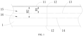
FIG. 1 is a schematic structural diagram of an emitter of a photovoltaic cell according to the present disclosure in one or more embodiments, in which a first plane and a second plane are each provided with a passivation layer. -
FIG. 2 shows a test curve of doping concentration of the emitter inFIG. 1 , in which a target element is boron. -
FIG. 3 is a schematic structural diagram after the emitter inFIG. 1 is coated with a doping reagent. -
FIG. 4 is a schematic diagram showing that the emitter inFIG. 3 is irradiated by first laser. -
FIG. 5 is a schematic diagram showing that the emitter inFIG. 4 is irradiated by second laser. -
FIG. 6 is a flowchart of a method for manufacturing a photovoltaic cell according to the present disclosure in one or more embodiments. - Reference signs:
- 1: substrate;
- 11: passivation layer;
- 12: first plane;
- 13: second plane;
- 14: third plane;
- 15: first doped layer;
- 16: second doped layer;
- 2: doping reagent;
- 3: first laser;
- 4: second laser.
- The accompanying drawings herein are incorporated in and constitute a part of this specification, illustrate embodiments consistent with the present disclosure and, together with the specification, serve to explain the principles of the present disclosure.
- In order to better understand the technical solutions of the present disclosure, embodiments of the present disclosure are described in detail below with reference to the accompanying drawings.
- It is to be made clear that the described embodiments are only some rather than all of the embodiments of the present disclosure. All other embodiments obtained by those of ordinary skill in the art based on the embodiments in the present disclosure without creative efforts fall within the protection scope of the present disclosure.
- The terms used in the embodiments of the present disclosure are intended only to describe particular embodiments and are not intended to limit the present disclosure. As used in the embodiments of the present disclosure and the appended claims, the singular forms of "a/an", "the", and "said" are intended to include plural forms, unless otherwise clearly specified by the context.
- It is to be understood that the term "and/or" used herein is merely an association relationship describing associated objects, indicating that three relationships may exist. For example, A and/or B indicates that there are three cases of A alone, A and B together, and B alone. In addition, the character "/" herein generally means that associated objects before and after it are in an "or" relationship.
- It is to be noted that the location terms such as "above", "below", "left", and "right" described in the embodiments of the present disclosure are described with reference to the angles shown in the accompanying drawings, and should not be construed as limitations on the embodiments of the present disclosure. In addition, in the context, it is to be further understood that, when one element is referred to as being connected "above" or "below" another element, the one element may be directly connected "above" or "below" another element, or connected "above" or "below" another element via an intermediate element.
- Some embodiments of the present disclosure provide a photovoltaic cell, including a substrate 1 (the
substrate 1 includes, but not limited to, an N-type silicon wafer, a P-type silicon wafer, and the like). As shown inFIG. 1 , an emitter and apassivation layer 11 stacked in sequence are included on one side of thesubstrate 1, the emitter is configured to connect a metal electrode, and thepassivation layer 11 keeps the lifetime of effective minority carriers of the photovoltaic cell at a relatively high level, such that the photovoltaic cell obtains a higher open-circuit voltage and a higher short-circuit voltage, which effectively improves output characteristics of the photovoltaic cell, and then improves conversion efficiency of the photovoltaic cell. Thesubstrate 1 may be made of a silicon substrate material, and the silicon substrate material may include one or more of monocrystalline silicon, polycrystalline silicon, amorphous silicon, and microcrystalline silicon. A specific material and a specific type of thesubstrate 1 are not limited in the present disclosure. - As shown in
FIG. 1 , the emitter includes a first dopedlayer 15 and a second dopedlayer 16 stacked along a thickness direction of the emmiter and containing a target element, the first dopedlayer 15 is part of the emitter between afirst plane 12 and asecond plane 13, and the second dopedlayer 16 is part of the emitter between athird plane 14 and thesecond plane 13. The target element includes, but is not limited to, nitrogen, phosphorus, arsenic, boron, aluminum, gallium, indium, thallium, and the like. If the substrate is an N-type semiconductor, the emitter may be a P-type doped layer. If the substrate is a P-type semiconductor, the emitter may be an N-type doped layer. A specific type of the target element is not limited in the present disclosure. The following descriptions are all based on an example in which thesubstrate 1 is a semiconductor silicon wafer and the target element is boron. - Within a unit volume, a rate of change ΔC1 between doping concentration of the
second plane 13 and doping concentration of thefirst plane 12 and a rate of change ΔC2 between doping concentration of thethird plane 14 and the doping concentration of thesecond plane 13 satisfy: ΔC1<ΔC2. That is, as shown inFIG. 2 , doping concentration of the first dopedlayer 15 and doping concentration of the second dopedlayer 16 change stepwise (that is, as shown inFIG. 2 , a doping concentration curve of the target element in this embodiment is stepwise). Compared with the related art on the basis of the target element with an equal amount, in the embodiments of the present disclosure, the doping concentration of the target element in the first dopedlayer 15 is increased, which is conducive to improving conductivity of the first dopedlayer 15, enables the metal electrode to form good ohmic contact with the first dopedlayer 15, reduces contact resistance between the metal electrode and the first dopedlayer 15, thereby facilitating transmission of more majority carriers to the metal electrode, and increases a fill factor of the cell, thereby improving photoelectric conversion efficiency of the photovoltaic cell. In addition, upon comparison with the related art on the basis of same doping concentration of the first dopedlayer 15, ΔC1<ΔC2 can reduce consumption of the doping reagent during the doping, thereby reducing manufacturing costs and a manufacturing cycle of the photovoltaic cell while ensuring stable operation of the photovoltaic cell. - The rate of change ΔC1 between the doping concentration of the
second plane 13 and the doping concentration of thefirst plane 12 satisfies: ΔC1≤15%. If ΔC1 is greater than 15%, a difference between the doping concentration of thesecond plane 13 and the doping concentration of thefirst plane 12 is relatively large. During subsequent sintering of the doped electrode, the target element diffuses along a thickness direction of thesubstrate 1 to a direction close to thesecond plane 12 under the action of a high temperature, such that the doping concentration of thefirst plane 12 is reduced, thereby affecting ohmic contact between the sintered metal electrode and the first dopedlayer 15. Therefore, ΔC1≤15% reduces a decrease rate of the doping concentration of the first dopedlayer 15 along the thickness direction, thereby reducing an influence of the subsequent sintering on the doping concentration of the first dopedlayer 15, such that the sintered metal electrode forms good ohmic contact with the first dopedlayer 15, thereby further improving the photoelectric conversion efficiency of the photovoltaic cell. - The rate of change ΔC2 between the doping concentration of the
third plane 14 and the doping concentration of thesecond plane 13 satisfies: ΔC2≤30%. If ΔC2 is greater than 30%, a difference between the doping concentration of thethird plane 14 and the doping concentration of thesecond plane 13 is relatively large. During subsequent sintering of the doped electrode, the target element in the first dopedlayer 15 diffuses along the thickness direction of thesubstrate 1 to a direction close to thethird plane 14 under the action of a high temperature, such that the doping concentration of thefirst plane 15 is reduced, thereby affecting ohmic contact between the sintered metal electrode and the first dopedlayer 15. Therefore, ΔC2≤0% further reduces the influence of the subsequent sintering on the doping concentration of the first dopedlayer 15, thereby further improving the photoelectric conversion efficiency of the photovoltaic cell. - In addition, within a unit volume, a rate of change ΔC3 between doping concentration at a first position of the
second plane 13 and doping concentration at a second position of thesecond plane 13 satisfies: ΔC3≤25%. In other words, concentration difference of doping concentration at any two positions on the second plane satisfies: ΔC3≤25%. If ΔC3>25%, during the subsequent sintering, at the first position with high doping concentration, the doping concentration of thefirst plane 12 at the first position changes less (that is, the concentration is reduced less). That is, the doping concentration of the first dopedlayer 15 at the first position changes less. At the second position with low doping concentration, the doping concentration of thefirst plane 12 at the second position changes more (that is, the concentration is reduced more). That is, the doping concentration of the first dopedlayer 15 at the second position changes more. As a result, contact resistance of connection between the sintered metal electrode and the emitter at the second position with low doping concentration is higher. Therefore, AC3≤25% improves consistency of the doping concentration of thesecond plane 13, thereby reducing a risk of low local doping concentration of the first dopedlayer 15 after sintering, so as to further reduce the contact resistance of the connection between the metal electrode and the emitter, and improve consistency of the contact resistance of the connection between the metal electrode and the emitter, thereby improving operation stability of the emitter and metal electrode. - For example, as shown in
FIG. 1 , a distance H1 between thesecond plane 13 and thefirst plane 12 satisfies: 0.25 µm≤H1≤0.40 µm, and a distance H2 between thethird plane 14 and thefirst plane 12 satisfies: 0.5 µm≤H2≤0.7 µm. In some embodiments, 0.30 µm≤H1≤0.35 µm. - If H1 and H2 are smaller (that is, H1<0.25 µm, and H2<0.5 µm), causing thicknesses of the first doped
layer 15 and the second dopedlayer 16 to be smaller, during the doping, the target element of the first dopedlayer 15 can diffuse to the second dopedlayer 16 within a short time, which is not conducive to controlling the doping concentration of the first dopedlayer 15 and the second dopedlayer 16. If H1 and H2 are larger (that is, H1>0.40 µm, and H2>0.7 µm), the thicknesses of the first dopedlayer 15 and the second dopedlayer 16 are larger, the target element diffuses more slowly in the first dopedlayer 15 and the second dopedlayer 16 and has a longer manufacturing cycle while it is not conducive to controlling the thicknesses of the first dopedlayer 15 and the second dopedlayer 16. Therefore, 0.25 µm≤H1≤0.40 µm and 0.5 µm≤H2≤0.7 µm can shorten a doping cycle while reducing doping difficulty and ensuring consistency between the doping concentration of the first dopedlayer 15 and the doping concentration of the second dopedlayer 16. - For the above photovoltaic cell, as shown in
FIG. 2 to FIG. 6 , according to a second aspect of the present disclosure, a method for manufacturing a photovoltaic cell is provided, including: doping a target element into thesubstrate 1 to form the emitter; and manufacturing thepassivation layer 11 on thefirst plane 12 of the emitter. - A manner of doping the target element includes, but not limited to, high-temperature doping, post-oxidation doping, laser doping, and the like. Laser doping is adopted in the present disclosure, so as to control a doping depth.
- For example, the doping a target element into the
substrate 1 includes: coating thefirst plane 12 with adoping reagent 2 containing the target element; directing afirst laser 3 through thedoping reagent 2 into thesecond plane 13 to diffuse the target element to the first dopedlayer 15 and the second dopedlayer 16; and directing asecond laser 4 through thedoping reagent 2 into thethird plane 14 to diffuse the target element of the second dopedlayer 16 to the first dopedlayer 15. - In this embodiment, first, the
first laser 3 is incident on thesecond plane 13, such that the target element is driven by thefirst laser 3 to enter the first dopedlayer 15 and diffuse to the second dopedlayer 16. In this case, the doping concentration of the first dopedlayer 15 varies greatly. That is, the doping concentration of the first dopedlayer 15 has poor consistency. Thesecond laser 4 is incident on thethird plane 14, such that the target element in the second dopedlayer 16 diffuses reversely to the first dopedlayer 15 to increase the concentration of the first dopedlayer 15 and diffuse the target element at a position with higher doping concentration inside the first dopedlayer 15 to a position with lower doping concentration, thereby improving the consistency of the doping concentration of the first dopedlayer 15. The target element is first doped into the first dopedlayer 15 and the second dopedlayer 16 by thefirst laser 3, and then the doping concentration of the first dopedlayer 15 and the second dopedlayer 16 is adjusted by thesecond laser 4, which simplifies the doping process of the emitter, thereby reducing a doping cycle and doping costs of the emitter. By use of laser doping, a risk of a decrease in the lifetime of the minority carriers caused by entry of impurities into thesubstrate 1 from a surface of thesubstrate 1 during the doping is reduced, thereby improving electrical properties of the photovoltaic cell. - For example, when the
first laser 3 is incident on thesecond plane 13, thefirst laser 3 can generate a high temperature on thesecond plane 13, such that the target element near thesecond plane 13 diffuses towards a direction away from the second plane 13 (that is, diffuses towards a direction close to thefirst plane 12 and a direction close to the third plane 14). When thesecond laser 4 is incident on thethird plane 14, thesecond laser 4 can generate a high temperature on thethird plane 14, such that the target element near thethird plane 14 diffuses toward a direction away from the third plane 14 (that is, diffuses towards a direction close to the first plane 12). - In this embodiment, local high temperatures generated by the
first laser 3 and thesecond laser 4 drive the diffusion of the target element, which simplifies a doping manner of the emitter, thereby reducing doping costs of the emitter. At the same time, a diffusion rate of the target element is increased, thereby reducing a manufacturing cycle of the emitter. - A wavelength L1 of the
first laser 3 satisfies: 300 nm≤L1≤400 nm, a wavelength L2 of thesecond laser 4 satisfies: 400 nm≤L2≤550 nm, and L1<L2. For example, L1=300nm, 350 nm, or 390 nm, and L2=400 nm, 450 nm, or 500 nm. - In this embodiment, the wavelength of the
first laser 3 is less than the wavelength of thesecond laser 4, such that a depth of thefirst laser 3 entering the emitter is less than a depth of thesecond laser 4 entering the emitter, which reduces a risk of failure of thesecond laser 4 caused by the depth of thesecond laser 4 entering the emitter being less than the depth of thefirst laser 3 entering the emitter, thereby improving operation stability of thefirst laser 3 and thesecond laser 4. 300 nm≤L1≤400 nm and 400 nm≤L2≤550 nm facilitate thefirst laser 3 to enter the presetsecond plane 13 and thesecond laser 4 to enter the presetthird plane 14, so as to facilitate the control over the doping concentration of the emitter. - In addition, energy density W1 of the
first laser 3 satisfies: 0.4 J/cm2≤W1≤1.5 J/cm2, and energy density W2 of thesecond laser 4 satisfies: 0.6 J/cm2≤W2≤1.8 J/cm2. - If the energy density of the
first laser 3 is lower (i.e., W1<0.4 J/cm2) and the energy density of thesecond laser 4 is lower (i.e., W2<0.6 J/cm2), heat generated by thefirst laser 3 on thesecond plane 13 and heat generated by thesecond laser 4 on thethird plane 14 are less, which reduces a diffusion rate of the target element. After the heat dissipates, the doping concentration of the first dopedlayer 15 and the second dopedlayer 16 changes less. If the energy density of thefirst laser 3 is higher (i.e., W1>1.5 J/cm2) and the energy density of thesecond laser 4 is higher (i.e.,W2>1.8 J /cm2), the heat generated by thefirst laser 3 on thesecond plane 13 and the heat generated by thesecond laser 4 on thethird plane 14 are more, such that the diffusion rate of the target element is higher. After the heat dissipates, the doping concentration of the first dopedlayer 15 and the second dopedlayer 16 changes more. Therefore, 0.4 J/cm2≤W1≤1.5 J/cm2 and 0.6 J/cm2≤W2≤1.8 J/cm2 can facilitate the control over the changes in the doping concentration before and after laser irradiation, thereby facilitating the realization of the consistency between the doping concentration of the first dopedlayer 15 and the second dopedlayer 16. - In any one of the above embodiments, the
first laser 3 and thesecond laser 4 can be emitted by a same laser emitter, to simplify operations during the manufacturing, and can also be emitted by different laser emitters, so as to adjust parameters such as the wavelengths and the energy density of thefirst laser 3 and thesecond laser 4. In addition, the laser emitter can emit more than three laser of different wavelengths, such that the laser emitter can dope the target element to doped layers with different depths. - The doped layers may further include a third doped layer (not shown in the figure), a fourth doped layer (not shown in the figure), a fifth doped layer (not shown in the figure), and the like. A number of the doped layers is not limited in the present disclosure. Correspondingly, the laser may further include a third laser (not shown in the figure), a fourth laser (not shown in the figure), a fifth laser, and the like with different wavelengths.
- To sum up, as shown in
FIG. 6 , the manufacturing method for the photovoltaic cell is as follows. - The surface of the
substrate 1 is textured, such that an antireflection texture is formed on the surface of thesubstrate 1, thereby reducing light reflectivity of the surface of thesubstrate 1, so as to increase a utilization rate of solar energy by the photovoltaic cell and then improve conversion efficiency of the photovoltaic cell. - As shown in
FIG. 3 , the surface of thesubstrate 1 is coated with adoping reagent 2 containing the target element. - As shown in
FIG. 4 , thefirst laser 3 passes through thedoping reagent 2 and thefirst plane 12 into thesecond plane 13, and generates a local high temperature on thesecond plane 13. In this case, driven by thefirst laser 3 and the local high temperature generated by thefirst laser 3, the target element in thedoping reagent 2 diffuses to the first dopedlayer 15 and the second dopedlayer 16. - As shown in
FIG. 5 , thesecond laser 4 passes through thedoping reagent 2, thefirst plane 12, and thesecond plane 13 into thethird plane 14, and generates a local high temperature on thethird plane 14. In this case, driven by the local high temperature generated by thesecond laser 4, the target element in the second dopedlayer 16 diffuses to the first dopedlayer 15, so as to increase the doping concentration of the first dopedlayer 15. - The remaining
doping reagent 2 is removed. - A back surface of the
substrate 1 away from the emitter is polished along a thickness direction of thesubstrate 1. - The
passivation layer 11 is manufactured on a surface of the emitter, so as to reduce activity of the surface of thesubstrate 1, increase a cleaning procedure for the surface, and reduce a risk of formation of a recombination center caused by introduction of impurities from the surface, thereby reducing a recombination rate of electrons and minority carriers and keeping the lifetime of effective minority carriers of the photovoltaic cell at a relatively high level, such that the photovoltaic cell obtains a higher open-circuit voltage and a higher short-circuit voltage, which effectively improves output characteristics of the photovoltaic cell, thereby improving the conversion efficiency of the photovoltaic cell. - Doping concentration of a double-laser doped emitter in the present disclosure, of an emitter doped by a post-oxidation process in Comparative Example 1, and of a single-laser doped emitter of Comparative Example 2 is detected, and after comparative analysis, a test curve of changes in the doping concentration as shown in
FIG. 2 (the target element is boron) and a table of parameters of the photovoltaic cell as shown in Table 1 (specific data of Comparative Example 2 is not recorded in the table) are obtained.Table 1 Table of parameters of photovoltaic cell Embodi ment Doping curve Doping concentrations (atom/cm3) Solar cell parameter Depth 0.4 (µm) Depth 0.5 (µm) Dept h 1.0 (µm) Resist ivity (mΩ·cm2) Fill factor (%) 1 Stepwise 1.30E +19 1.00E +19 < 3E+ 171.3 83.5 Compar ative Example 1 Conventi onal 1.00E +19 6.00E +18 < 3E+ 171.6 83.2 - As can be seen from
FIG. 2 and Table 1, in Comparative Example 1 (doping is performed by a post-oxidation doping process), a difference between doping concentration of a first comparison plane (that is, at a depth of 0.4 µm in the table) and doping concentration of a second comparison plane (that is, at a depth of 0.5 µm in the table) is large, while in an embodiment of the present disclosure (i.e., Embodiment 1), a difference between doping concentration of a first detection plane (that is, at a depth of 0.4 µm in the table) and doping concentration of a second detection plane (that is, at a depth of 0.5 µm in the table) is small. Thus, compared with the post-oxidation doping process, consistency of the doping concentration of the double-laser doping in this embodiment of the present application is higher, such that the emitter has lower resistivity, which is conducive to the ohmic contact between the metal electrode and the emitter, and increases the fill factor of the photovoltaic cell, thereby improving the conversion efficiency of the photovoltaic cell. - The above are merely preferred embodiments of the present disclosure, and are not intended to limit the present disclosure. For those skilled in the art, the present disclosure may be subject to various modifications and changes.
Claims (15)
- A photovoltaic cell, comprising:a substrate (1) comprising an emitter disposed in the substrate, anda passivation layer (11) stacked on a side of the emitter away from the substrate;wherein the emitter comprises a first plane (12) and a second plane (13) laminated along a thickness direction of the emitter, and part of the emitter between the second plane (13) and the first plane (12) is a first doped layer (15); andwithin a unit volume, a rate of change ΔC1 between doping concentration of the second plane (13) and doping concentration of the first plane (12) satisfies: ΔC1≤15%.
- The photovoltaic cell according to claim 1, whereina third plane (14) is provided on a side of the second plane (13) away from the first plane (12), and part of the emitter between the third plane (14) and the second plane (13) is a second doped layer (16); anda rate of change ΔC2 between doping concentration of the third plane (14) and the doping concentration of the second plane (13) satisfies: ΔC2≤30%.
- The photovoltaic cell according to claim 2, wherein
the rate of change ΔC1 between doping concentration of the second plane (13) and doping concentration of the first plane (12) and the rate of change ΔC2 between doping concentration of the third plane (14) and the doping concentration of the second plane (13) within a unit volume satisfy: ΔC1<ΔC2. - The photovoltaic cell according to claim 2, wherein
a target element in the first doped layer (15) and the second doped layer (16) comprises, but not limited to, nitrogen, phosphorus, arsenic, boron, aluminum, gallium, indium, thallium. - The photovoltaic cell according to claim 2, wherein a distance H1 between the second plane (13) and the first plane (12) satisfies: 0.3 µm≤H1≤0.35 µm; and
a distance H2 between the third plane (14) and the first plane (12) satisfies: 0.5 µm≤H2≤.7 µm. - The photovoltaic cell according to claim 1, wherein, within a unit volume, a rate of change ΔC3 between doping concentration at a first position of the second plane (13) and doping concentration at a second position of the second plane (13) satisfies: ΔC3≤25%.
- A method for manufacturing the photovoltaic cell according to claim 1, comprising:doping a target element into the substrate (1) to form the emitter; andmanufacturing the passivation layer on the first plane (12) of the emitter.
- The method according to claim 7, wherein a manner of doping the target element includes, but not limited to, high-temperature doping, post-oxidation doping, laser doping, and the like. Laser doping is adopted in the present disclosure, so as to control a doping depth.
- The method according to claim 7, wherein a third plane (14) is provided on a side of the second plane (13) away from the first plane (12), and said doping a target element into the substrate (1) comprises:coating the first plane (12) with a doping reagent (2) containing the target element;directing a first laser (3) through the doping reagent (2) into the second plane (13) to diffuse the target element to the first doped layer (15) and the second doped layer (16); anddirecting a second laser (4) through the doping reagent (2) into the third plane (14) to diffuse the target element of the second doped layer (16) to the first doped layer (15).
- The method according to claim 9, wherein said directing a first laser (3) through the doping reagent (2) into the second plane (13) to diffuse the target element to the first doped layer (15) and the second doped layer (16) comprises:directing the first laser (3) through the doping reagent (2) and the first plane (12) into the second plane (13), and generating a high temperature; anddriving the target element into the first doped layer (15) by the first laser (3) and further driving the target element to be diffused to the second doped layer (16) by the high temperature generated by the first laser (3).
- The method according to claim 10, wherein the first laser (3) and the second laser (4) are emitted by different laser emitters, and one of the laser emitters emits more than three laser of different wavelengths.
- The method according to claim 9, wherein said directing a second laser (4) through the doping reagent (2) into the third plane (14) to diffuse the target element of the second doped layer (16) to the first doped layer (15) comprises:directing the second laser (4) through the doping reagent (2), the first plane (12), and the second plane (13) into the third plane (14), and generating a high temperature; anddriving the target element to be diffused to the first doped layer (15) by the high temperature generated by the second laser (4).
- The method according to claim 9, wherein a wavelength L1 of the first laser (3) satisfies: 300 nm≤L1≤400 nm, a wavelength L2 of the second laser (4) satisfies: 400 nm≤L2≤550 nm, and L1<L2.
- The method according to claim 9, wherein energy density W1 of the first laser (3) satisfies: 0.4 J/cm2≤W1≤1.5 J/cm2, and energy density W2 of the second laser (4) satisfies: 0.6 J/cm2≤W2≤1.8 J/cm2.
- The method according to claim 9, wherein, after said doping the target element, the method further comprises:
removing the doping reagent (2) remaining on the first plane (12).
Applications Claiming Priority (1)
| Application Number | Priority Date | Filing Date | Title |
|---|---|---|---|
| CN202210874050.7A CN114975652B (en) | 2022-07-25 | 2022-07-25 | Photovoltaic cell and manufacturing method thereof |
Publications (2)
| Publication Number | Publication Date |
|---|---|
| EP4312278A1 true EP4312278A1 (en) | 2024-01-31 |
| EP4312278B1 EP4312278B1 (en) | 2025-02-26 |
Family
ID=82970339
Family Applications (1)
| Application Number | Title | Priority Date | Filing Date |
|---|---|---|---|
| EP23187575.8A Active EP4312278B1 (en) | 2022-07-25 | 2023-07-25 | Photovoltaic cell and manufacturing method for photovoltaic cell |
Country Status (2)
| Country | Link |
|---|---|
| EP (1) | EP4312278B1 (en) |
| CN (1) | CN114975652B (en) |
Families Citing this family (1)
| Publication number | Priority date | Publication date | Assignee | Title |
|---|---|---|---|---|
| CN115995502A (en) * | 2021-10-25 | 2023-04-21 | 天合光能股份有限公司 | Emitter, preparation method of selective emitter battery and selective emitter battery |
Citations (1)
| Publication number | Priority date | Publication date | Assignee | Title |
|---|---|---|---|---|
| US20150017793A1 (en) * | 2012-03-29 | 2015-01-15 | Newsouth Innovations Pty Limited | Formation of localised molten regions in silicon containing multiple impurity types |
Family Cites Families (19)
| Publication number | Priority date | Publication date | Assignee | Title |
|---|---|---|---|---|
| DE1439481A1 (en) * | 1964-12-01 | 1968-11-21 | Siemens Ag | transistor |
| JPH065741B2 (en) * | 1983-02-18 | 1994-01-19 | 株式会社日立製作所 | Planar type semiconductor device manufacturing method |
| US8247254B2 (en) * | 2007-07-13 | 2012-08-21 | Silicon China (HK) Ltd. | System and method for forming solar cell structures |
| KR20100050510A (en) * | 2007-07-20 | 2010-05-13 | 비피 코포레이션 노쓰 아메리카 인코포레이티드 | Methods for manufacturing cast silicon from seed crystals |
| US7838400B2 (en) * | 2008-07-17 | 2010-11-23 | Applied Materials, Inc. | Rapid thermal oxide passivated solar cell with improved junction |
| DE102008055941A1 (en) * | 2008-11-05 | 2010-06-17 | Osram Opto Semiconductors Gmbh | Surface emitting semiconductor laser device having a vertical emission direction |
| US8053343B2 (en) * | 2009-02-05 | 2011-11-08 | Snt. Co., Ltd. | Method for forming selective emitter of solar cell and diffusion apparatus for forming the same |
| KR101521104B1 (en) * | 2009-05-15 | 2015-05-20 | 주식회사 디엠에스 | Diffusion apparatus for forming the selective emitter |
| KR101145928B1 (en) * | 2009-03-11 | 2012-05-15 | 엘지전자 주식회사 | Solar Cell and Manufacturing Method of the same |
| KR101139443B1 (en) * | 2009-09-04 | 2012-04-30 | 엘지전자 주식회사 | Hetero-junction solar cell and fabrication method thereof |
| DE102010010813A1 (en) * | 2010-03-03 | 2011-09-08 | Centrotherm Photovoltaics Ag | Method for doping a semiconductor substrate and solar cell with two-stage doping |
| CN102185005A (en) * | 2010-10-18 | 2011-09-14 | 江阴浚鑫科技有限公司 | Method for manufacturing selective emitter battery |
| WO2012136848A1 (en) * | 2011-04-06 | 2012-10-11 | Abb Technology Ag | Bipolar punch-through semiconductor device and method for manufacturing such a semiconductor device |
| FR2988908B1 (en) * | 2012-04-03 | 2015-03-27 | Commissariat Energie Atomique | METHOD FOR MANUFACTURING A PHOTOVOLTAIC CELL WITH REAR-FACED INTERFIGITE CONTACTS |
| KR101363141B1 (en) * | 2012-06-29 | 2014-02-18 | 주식회사 신성솔라에너지 | Method for manufacturing solar cell |
| KR102010390B1 (en) * | 2013-05-28 | 2019-08-13 | 엘지전자 주식회사 | Method for manufacturing solar cell and dopant region thereof |
| JP2018010896A (en) * | 2016-07-11 | 2018-01-18 | 株式会社村田製作所 | Heterojunction bipolar transistor |
| CN108899376B (en) * | 2018-07-03 | 2020-09-04 | 浙江晶科能源有限公司 | A kind of solar cell and its selective emitter structure fabrication method |
| CN113571604B (en) * | 2021-09-27 | 2022-01-25 | 浙江晶科能源有限公司 | Photovoltaic cell, preparation method thereof and photovoltaic module |
-
2022
- 2022-07-25 CN CN202210874050.7A patent/CN114975652B/en active Active
-
2023
- 2023-07-25 EP EP23187575.8A patent/EP4312278B1/en active Active
Patent Citations (1)
| Publication number | Priority date | Publication date | Assignee | Title |
|---|---|---|---|---|
| US20150017793A1 (en) * | 2012-03-29 | 2015-01-15 | Newsouth Innovations Pty Limited | Formation of localised molten regions in silicon containing multiple impurity types |
Non-Patent Citations (3)
| Title |
|---|
| HAO RUIYING ET AL: "Kerfless Epitaxial Mono Crystalline Si Wafers With Built-In Junction and From Reused Substrates for High-Efficiency PERx Cells", IEEE JOURNAL OF PHOTOVOLTAICS, IEEE, vol. 6, no. 6, 1 November 2016 (2016-11-01), pages 1451 - 1455, XP011626412, ISSN: 2156-3381, [retrieved on 20161020], DOI: 10.1109/JPHOTOV.2016.2601945 * |
| MONDAL SOM ET AL: "Deep Diffusion of Phosphorus in Silicon using Microsecond-pulsed Laser Doping", MATERIALS SCIENCE IN SEMICONDUCTOR PROCESSING, vol. 59, 30 November 2016 (2016-11-30), pages 10 - 17, XP029859904, ISSN: 1369-8001, DOI: 10.1016/J.MSSP.2016.11.011 * |
| ZHOU ZIBO ET AL: "Rapid, deep dopant diffusion in crystalline silicon by laser-induced surface melting", MATERIALS SCIENCE IN SEMICONDUCTOR PROCESSING, ELSEVIER SCIENCE PUBLISHERS B.V., BARKING, UK, vol. 86, 20 June 2018 (2018-06-20), pages 8 - 17, XP085420394, ISSN: 1369-8001, DOI: 10.1016/J.MSSP.2018.06.012 * |
Also Published As
| Publication number | Publication date |
|---|---|
| CN114975652B (en) | 2022-12-23 |
| CN114975652A (en) | 2022-08-30 |
| US20240030371A1 (en) | 2024-01-25 |
| EP4312278B1 (en) | 2025-02-26 |
Similar Documents
| Publication | Publication Date | Title |
|---|---|---|
| JP2023124756A (en) | SOLAR CELL AND MANUFACTURING METHOD THEREOF, PHOTOVOLTAIC MODULE | |
| KR101626248B1 (en) | Silicon solar cell and method of manufacturing the same | |
| CN1826699B (en) | Silicon thin film solar cells | |
| US20120055547A1 (en) | High-efficiency solar cell structures and methods of manufacture | |
| JP2024155655A (en) | Solar cell and its manufacturing method, photovoltaic module | |
| US20240258441A1 (en) | Method for making solar cell and solar cell | |
| CN117727838B (en) | Solar cell, preparation method thereof and photovoltaic module | |
| NL2033696B1 (en) | Solar cell and production method thereof, photovoltaic module | |
| WO2023124048A1 (en) | Heterojunction solar cell, preparation method thereof and power generation apparatus | |
| CN103985773A (en) | Silicon crystal solar cell structure | |
| CN102487102B (en) | Solar cell and preparation method thereof | |
| US20250311481A1 (en) | Solar cell, method for manufacturing the same, and photovoltaic module | |
| CN114050105A (en) | TopCon battery preparation method | |
| CN111106188B (en) | N-type battery, preparation method of selective emitter of N-type battery and N-type battery | |
| CN116093191A (en) | Solar cell and photovoltaic module | |
| CN116864548A (en) | P-type back junction TOPCON battery and preparation method thereof | |
| EP4312278A1 (en) | Photovoltaic cell and manufacturing method for photovoltaic cell | |
| CN121152411B (en) | A solar cell and photovoltaic module | |
| CN218730968U (en) | Solar cell and photovoltaic module | |
| JP2024022416A (en) | Solar cells and solar cell manufacturing methods, photovoltaic modules | |
| US12622087B2 (en) | Photovoltaic cell and manufacturing method for photovoltaic cell | |
| EP4683464A1 (en) | Metal-semiconductor contact structure, solar cell and photovoltaic module | |
| CN119384095A (en) | A metallized back contact solar cell structure and manufacturing method | |
| KR101080344B1 (en) | Method of preparing selective emitter of solar cell and method of manufacturing solar cell | |
| Yu et al. | Improved Bifacial Properties of P‐Type Passivated Emitter and Rear Cell Solar Cells toward High Mass Production Efficiency |
Legal Events
| Date | Code | Title | Description |
|---|---|---|---|
| PUAI | Public reference made under article 153(3) epc to a published international application that has entered the european phase |
Free format text: ORIGINAL CODE: 0009012 |
|
| STAA | Information on the status of an ep patent application or granted ep patent |
Free format text: STATUS: REQUEST FOR EXAMINATION WAS MADE |
|
| 17P | Request for examination filed |
Effective date: 20230725 |
|
| AK | Designated contracting states |
Kind code of ref document: A1 Designated state(s): AL AT BE BG CH CY CZ DE DK EE ES FI FR GB GR HR HU IE IS IT LI LT LU LV MC ME MK MT NL NO PL PT RO RS SE SI SK SM TR |
|
| GRAP | Despatch of communication of intention to grant a patent |
Free format text: ORIGINAL CODE: EPIDOSNIGR1 |
|
| STAA | Information on the status of an ep patent application or granted ep patent |
Free format text: STATUS: GRANT OF PATENT IS INTENDED |
|
| RIC1 | Information provided on ipc code assigned before grant |
Ipc: H01L 31/18 20060101ALI20241025BHEP Ipc: H01L 31/068 20120101ALI20241025BHEP Ipc: H01L 31/0288 20060101AFI20241025BHEP |
|
| INTG | Intention to grant announced |
Effective date: 20241112 |
|
| GRAS | Grant fee paid |
Free format text: ORIGINAL CODE: EPIDOSNIGR3 |
|
| GRAA | (expected) grant |
Free format text: ORIGINAL CODE: 0009210 |
|
| STAA | Information on the status of an ep patent application or granted ep patent |
Free format text: STATUS: THE PATENT HAS BEEN GRANTED |
|
| AK | Designated contracting states |
Kind code of ref document: B1 Designated state(s): AL AT BE BG CH CY CZ DE DK EE ES FI FR GB GR HR HU IE IS IT LI LT LU LV MC ME MK MT NL NO PL PT RO RS SE SI SK SM TR |
|
| REG | Reference to a national code |
Ref country code: GB Ref legal event code: FG4D |
|
| REG | Reference to a national code |
Ref country code: DE Ref legal event code: R096 Ref document number: 602023002189 Country of ref document: DE |
|
| REG | Reference to a national code |
Ref country code: IE Ref legal event code: FG4D |
|
| REG | Reference to a national code |
Ref country code: NL Ref legal event code: MP Effective date: 20250226 |
|
| PG25 | Lapsed in a contracting state [announced via postgrant information from national office to epo] |
Ref country code: RS Free format text: LAPSE BECAUSE OF FAILURE TO SUBMIT A TRANSLATION OF THE DESCRIPTION OR TO PAY THE FEE WITHIN THE PRESCRIBED TIME-LIMIT Effective date: 20250526 |
|
| PG25 | Lapsed in a contracting state [announced via postgrant information from national office to epo] |
Ref country code: FI Free format text: LAPSE BECAUSE OF FAILURE TO SUBMIT A TRANSLATION OF THE DESCRIPTION OR TO PAY THE FEE WITHIN THE PRESCRIBED TIME-LIMIT Effective date: 20250226 |
|
| PG25 | Lapsed in a contracting state [announced via postgrant information from national office to epo] |
Ref country code: PL Free format text: LAPSE BECAUSE OF FAILURE TO SUBMIT A TRANSLATION OF THE DESCRIPTION OR TO PAY THE FEE WITHIN THE PRESCRIBED TIME-LIMIT Effective date: 20250226 |
|
| PG25 | Lapsed in a contracting state [announced via postgrant information from national office to epo] |
Ref country code: ES Free format text: LAPSE BECAUSE OF FAILURE TO SUBMIT A TRANSLATION OF THE DESCRIPTION OR TO PAY THE FEE WITHIN THE PRESCRIBED TIME-LIMIT Effective date: 20250226 |
|
| REG | Reference to a national code |
Ref country code: LT Ref legal event code: MG9D |
|
| PG25 | Lapsed in a contracting state [announced via postgrant information from national office to epo] |
Ref country code: NO Free format text: LAPSE BECAUSE OF FAILURE TO SUBMIT A TRANSLATION OF THE DESCRIPTION OR TO PAY THE FEE WITHIN THE PRESCRIBED TIME-LIMIT Effective date: 20250526 Ref country code: IS Free format text: LAPSE BECAUSE OF FAILURE TO SUBMIT A TRANSLATION OF THE DESCRIPTION OR TO PAY THE FEE WITHIN THE PRESCRIBED TIME-LIMIT Effective date: 20250626 |
|
| PG25 | Lapsed in a contracting state [announced via postgrant information from national office to epo] |
Ref country code: NL Free format text: LAPSE BECAUSE OF FAILURE TO SUBMIT A TRANSLATION OF THE DESCRIPTION OR TO PAY THE FEE WITHIN THE PRESCRIBED TIME-LIMIT Effective date: 20250226 |
|
| PG25 | Lapsed in a contracting state [announced via postgrant information from national office to epo] |
Ref country code: HR Free format text: LAPSE BECAUSE OF FAILURE TO SUBMIT A TRANSLATION OF THE DESCRIPTION OR TO PAY THE FEE WITHIN THE PRESCRIBED TIME-LIMIT Effective date: 20250226 |
|
| PG25 | Lapsed in a contracting state [announced via postgrant information from national office to epo] |
Ref country code: PT Free format text: LAPSE BECAUSE OF FAILURE TO SUBMIT A TRANSLATION OF THE DESCRIPTION OR TO PAY THE FEE WITHIN THE PRESCRIBED TIME-LIMIT Effective date: 20250626 Ref country code: LV Free format text: LAPSE BECAUSE OF FAILURE TO SUBMIT A TRANSLATION OF THE DESCRIPTION OR TO PAY THE FEE WITHIN THE PRESCRIBED TIME-LIMIT Effective date: 20250226 |
|
| PG25 | Lapsed in a contracting state [announced via postgrant information from national office to epo] |
Ref country code: BG Free format text: LAPSE BECAUSE OF FAILURE TO SUBMIT A TRANSLATION OF THE DESCRIPTION OR TO PAY THE FEE WITHIN THE PRESCRIBED TIME-LIMIT Effective date: 20250226 Ref country code: GR Free format text: LAPSE BECAUSE OF FAILURE TO SUBMIT A TRANSLATION OF THE DESCRIPTION OR TO PAY THE FEE WITHIN THE PRESCRIBED TIME-LIMIT Effective date: 20250527 |
|
| REG | Reference to a national code |
Ref country code: AT Ref legal event code: MK05 Ref document number: 1771568 Country of ref document: AT Kind code of ref document: T Effective date: 20250226 |
|
| PG25 | Lapsed in a contracting state [announced via postgrant information from national office to epo] |
Ref country code: SE Free format text: LAPSE BECAUSE OF FAILURE TO SUBMIT A TRANSLATION OF THE DESCRIPTION OR TO PAY THE FEE WITHIN THE PRESCRIBED TIME-LIMIT Effective date: 20250226 |
|
| PG25 | Lapsed in a contracting state [announced via postgrant information from national office to epo] |
Ref country code: SM Free format text: LAPSE BECAUSE OF FAILURE TO SUBMIT A TRANSLATION OF THE DESCRIPTION OR TO PAY THE FEE WITHIN THE PRESCRIBED TIME-LIMIT Effective date: 20250226 |
|
| PG25 | Lapsed in a contracting state [announced via postgrant information from national office to epo] |
Ref country code: DK Free format text: LAPSE BECAUSE OF FAILURE TO SUBMIT A TRANSLATION OF THE DESCRIPTION OR TO PAY THE FEE WITHIN THE PRESCRIBED TIME-LIMIT Effective date: 20250226 |
|
| PGFP | Annual fee paid to national office [announced via postgrant information from national office to epo] |
Ref country code: DE Payment date: 20250722 Year of fee payment: 3 |
|
| PG25 | Lapsed in a contracting state [announced via postgrant information from national office to epo] |
Ref country code: IT Free format text: LAPSE BECAUSE OF FAILURE TO SUBMIT A TRANSLATION OF THE DESCRIPTION OR TO PAY THE FEE WITHIN THE PRESCRIBED TIME-LIMIT Effective date: 20250226 |
|
| PG25 | Lapsed in a contracting state [announced via postgrant information from national office to epo] |
Ref country code: AT Free format text: LAPSE BECAUSE OF FAILURE TO SUBMIT A TRANSLATION OF THE DESCRIPTION OR TO PAY THE FEE WITHIN THE PRESCRIBED TIME-LIMIT Effective date: 20250226 |
|
| PG25 | Lapsed in a contracting state [announced via postgrant information from national office to epo] |
Ref country code: CZ Free format text: LAPSE BECAUSE OF FAILURE TO SUBMIT A TRANSLATION OF THE DESCRIPTION OR TO PAY THE FEE WITHIN THE PRESCRIBED TIME-LIMIT Effective date: 20250226 Ref country code: EE Free format text: LAPSE BECAUSE OF FAILURE TO SUBMIT A TRANSLATION OF THE DESCRIPTION OR TO PAY THE FEE WITHIN THE PRESCRIBED TIME-LIMIT Effective date: 20250226 |
|
| PG25 | Lapsed in a contracting state [announced via postgrant information from national office to epo] |
Ref country code: RO Free format text: LAPSE BECAUSE OF FAILURE TO SUBMIT A TRANSLATION OF THE DESCRIPTION OR TO PAY THE FEE WITHIN THE PRESCRIBED TIME-LIMIT Effective date: 20250226 |
|
| PG25 | Lapsed in a contracting state [announced via postgrant information from national office to epo] |
Ref country code: SK Free format text: LAPSE BECAUSE OF FAILURE TO SUBMIT A TRANSLATION OF THE DESCRIPTION OR TO PAY THE FEE WITHIN THE PRESCRIBED TIME-LIMIT Effective date: 20250226 |
|
| REG | Reference to a national code |
Ref country code: DE Ref legal event code: R097 Ref document number: 602023002189 Country of ref document: DE |
|
| PLBE | No opposition filed within time limit |
Free format text: ORIGINAL CODE: 0009261 |
|
| STAA | Information on the status of an ep patent application or granted ep patent |
Free format text: STATUS: NO OPPOSITION FILED WITHIN TIME LIMIT |
|
| 26N | No opposition filed |
Effective date: 20251127 |
|
| PG25 | Lapsed in a contracting state [announced via postgrant information from national office to epo] |
Ref country code: LU Free format text: LAPSE BECAUSE OF NON-PAYMENT OF DUE FEES Effective date: 20250725 |
|
| REG | Reference to a national code |
Ref country code: BE Ref legal event code: MM Effective date: 20250731 |
|
| PG25 | Lapsed in a contracting state [announced via postgrant information from national office to epo] |
Ref country code: BE Free format text: LAPSE BECAUSE OF NON-PAYMENT OF DUE FEES Effective date: 20250731 |
|
| PG25 | Lapsed in a contracting state [announced via postgrant information from national office to epo] |
Ref country code: FR Free format text: LAPSE BECAUSE OF NON-PAYMENT OF DUE FEES Effective date: 20250731 |