EP4311045A1 - Photonic crystal semiconductor laser device and method for manufacturing same - Google Patents
Photonic crystal semiconductor laser device and method for manufacturing same Download PDFInfo
- Publication number
- EP4311045A1 EP4311045A1 EP22771781.6A EP22771781A EP4311045A1 EP 4311045 A1 EP4311045 A1 EP 4311045A1 EP 22771781 A EP22771781 A EP 22771781A EP 4311045 A1 EP4311045 A1 EP 4311045A1
- Authority
- EP
- European Patent Office
- Prior art keywords
- layer
- type
- photonic crystal
- type clad
- laser device
- Prior art date
- Legal status (The legal status is an assumption and is not a legal conclusion. Google has not performed a legal analysis and makes no representation as to the accuracy of the status listed.)
- Pending
Links
Images





Classifications
-
- H—ELECTRICITY
- H01—ELECTRIC ELEMENTS
- H01S—DEVICES USING THE PROCESS OF LIGHT AMPLIFICATION BY STIMULATED EMISSION OF RADIATION [LASER] TO AMPLIFY OR GENERATE LIGHT; DEVICES USING STIMULATED EMISSION OF ELECTROMAGNETIC RADIATION IN WAVE RANGES OTHER THAN OPTICAL
- H01S5/00—Semiconductor lasers
- H01S5/04—Processes or apparatus for excitation, e.g. pumping, e.g. by electron beams
- H01S5/042—Electrical excitation ; Circuits therefor
- H01S5/0425—Electrodes, e.g. characterised by the structure
-
- H—ELECTRICITY
- H01—ELECTRIC ELEMENTS
- H01S—DEVICES USING THE PROCESS OF LIGHT AMPLIFICATION BY STIMULATED EMISSION OF RADIATION [LASER] TO AMPLIFY OR GENERATE LIGHT; DEVICES USING STIMULATED EMISSION OF ELECTROMAGNETIC RADIATION IN WAVE RANGES OTHER THAN OPTICAL
- H01S5/00—Semiconductor lasers
- H01S5/30—Structure or shape of the active region; Materials used for the active region
- H01S5/32—Structure or shape of the active region; Materials used for the active region comprising PN junctions, e.g. hetero- or double- heterostructures
- H01S5/323—Structure or shape of the active region; Materials used for the active region comprising PN junctions, e.g. hetero- or double- heterostructures in AIIIBV compounds, e.g. AlGaAs-laser, InP-based laser
-
- H—ELECTRICITY
- H01—ELECTRIC ELEMENTS
- H01S—DEVICES USING THE PROCESS OF LIGHT AMPLIFICATION BY STIMULATED EMISSION OF RADIATION [LASER] TO AMPLIFY OR GENERATE LIGHT; DEVICES USING STIMULATED EMISSION OF ELECTROMAGNETIC RADIATION IN WAVE RANGES OTHER THAN OPTICAL
- H01S5/00—Semiconductor lasers
- H01S5/04—Processes or apparatus for excitation, e.g. pumping, e.g. by electron beams
- H01S5/042—Electrical excitation ; Circuits therefor
- H01S5/0425—Electrodes, e.g. characterised by the structure
- H01S5/04256—Electrodes, e.g. characterised by the structure characterised by the configuration
-
- H—ELECTRICITY
- H01—ELECTRIC ELEMENTS
- H01S—DEVICES USING THE PROCESS OF LIGHT AMPLIFICATION BY STIMULATED EMISSION OF RADIATION [LASER] TO AMPLIFY OR GENERATE LIGHT; DEVICES USING STIMULATED EMISSION OF ELECTROMAGNETIC RADIATION IN WAVE RANGES OTHER THAN OPTICAL
- H01S5/00—Semiconductor lasers
- H01S5/10—Construction or shape of the optical resonator, e.g. extended or external cavity, coupled cavities, bent-guide, varying width, thickness or composition of the active region
- H01S5/11—Comprising a photonic bandgap structure
-
- H—ELECTRICITY
- H01—ELECTRIC ELEMENTS
- H01S—DEVICES USING THE PROCESS OF LIGHT AMPLIFICATION BY STIMULATED EMISSION OF RADIATION [LASER] TO AMPLIFY OR GENERATE LIGHT; DEVICES USING STIMULATED EMISSION OF ELECTROMAGNETIC RADIATION IN WAVE RANGES OTHER THAN OPTICAL
- H01S5/00—Semiconductor lasers
- H01S5/20—Structure or shape of the semiconductor body to guide the optical wave ; Confining structures perpendicular to the optical axis, e.g. index or gain guiding, stripe geometry, broad area lasers, gain tailoring, transverse or lateral reflectors, special cladding structures, MQW barrier reflection layers
- H01S5/22—Structure or shape of the semiconductor body to guide the optical wave ; Confining structures perpendicular to the optical axis, e.g. index or gain guiding, stripe geometry, broad area lasers, gain tailoring, transverse or lateral reflectors, special cladding structures, MQW barrier reflection layers having a ridge or stripe structure
- H01S5/2205—Structure or shape of the semiconductor body to guide the optical wave ; Confining structures perpendicular to the optical axis, e.g. index or gain guiding, stripe geometry, broad area lasers, gain tailoring, transverse or lateral reflectors, special cladding structures, MQW barrier reflection layers having a ridge or stripe structure comprising special burying or current confinement layers
- H01S5/2218—Structure or shape of the semiconductor body to guide the optical wave ; Confining structures perpendicular to the optical axis, e.g. index or gain guiding, stripe geometry, broad area lasers, gain tailoring, transverse or lateral reflectors, special cladding structures, MQW barrier reflection layers having a ridge or stripe structure comprising special burying or current confinement layers having special optical properties
- H01S5/222—Structure or shape of the semiconductor body to guide the optical wave ; Confining structures perpendicular to the optical axis, e.g. index or gain guiding, stripe geometry, broad area lasers, gain tailoring, transverse or lateral reflectors, special cladding structures, MQW barrier reflection layers having a ridge or stripe structure comprising special burying or current confinement layers having special optical properties having a refractive index lower than that of the cladding layers or outer guiding layers
-
- H—ELECTRICITY
- H01—ELECTRIC ELEMENTS
- H01S—DEVICES USING THE PROCESS OF LIGHT AMPLIFICATION BY STIMULATED EMISSION OF RADIATION [LASER] TO AMPLIFY OR GENERATE LIGHT; DEVICES USING STIMULATED EMISSION OF ELECTROMAGNETIC RADIATION IN WAVE RANGES OTHER THAN OPTICAL
- H01S5/00—Semiconductor lasers
- H01S5/30—Structure or shape of the active region; Materials used for the active region
- H01S5/34—Structure or shape of the active region; Materials used for the active region comprising quantum well or superlattice structures, e.g. single quantum well [SQW] lasers, multiple quantum well [MQW] lasers or graded index separate confinement heterostructure [GRINSCH] lasers
- H01S5/343—Structure or shape of the active region; Materials used for the active region comprising quantum well or superlattice structures, e.g. single quantum well [SQW] lasers, multiple quantum well [MQW] lasers or graded index separate confinement heterostructure [GRINSCH] lasers in AIIIBV compounds, e.g. AlGaAs-laser, InP-based laser
-
- H—ELECTRICITY
- H01—ELECTRIC ELEMENTS
- H01S—DEVICES USING THE PROCESS OF LIGHT AMPLIFICATION BY STIMULATED EMISSION OF RADIATION [LASER] TO AMPLIFY OR GENERATE LIGHT; DEVICES USING STIMULATED EMISSION OF ELECTROMAGNETIC RADIATION IN WAVE RANGES OTHER THAN OPTICAL
- H01S5/00—Semiconductor lasers
- H01S5/02—Structural details or components not essential to laser action
- H01S5/0206—Substrates, e.g. growth, shape, material, removal or bonding
- H01S5/0215—Bonding to the substrate
-
- H—ELECTRICITY
- H01—ELECTRIC ELEMENTS
- H01S—DEVICES USING THE PROCESS OF LIGHT AMPLIFICATION BY STIMULATED EMISSION OF RADIATION [LASER] TO AMPLIFY OR GENERATE LIGHT; DEVICES USING STIMULATED EMISSION OF ELECTROMAGNETIC RADIATION IN WAVE RANGES OTHER THAN OPTICAL
- H01S5/00—Semiconductor lasers
- H01S5/02—Structural details or components not essential to laser action
- H01S5/0206—Substrates, e.g. growth, shape, material, removal or bonding
- H01S5/0217—Removal of the substrate
-
- H—ELECTRICITY
- H01—ELECTRIC ELEMENTS
- H01S—DEVICES USING THE PROCESS OF LIGHT AMPLIFICATION BY STIMULATED EMISSION OF RADIATION [LASER] TO AMPLIFY OR GENERATE LIGHT; DEVICES USING STIMULATED EMISSION OF ELECTROMAGNETIC RADIATION IN WAVE RANGES OTHER THAN OPTICAL
- H01S5/00—Semiconductor lasers
- H01S5/02—Structural details or components not essential to laser action
- H01S5/022—Mountings; Housings
- H01S5/0233—Mounting configuration of laser chips
- H01S5/0234—Up-side down mountings, e.g. Flip-chip, epi-side down mountings or junction down mountings
Definitions
- the embodiments of the present invention relate to an active optical device, and more particularly, to a semiconductor laser.
- the embodiments of the present invention relate to a laser device for electrically driving a photonic crystal laser.
- a photonic crystal refers to a structure in which two materials having different refractive index are periodically arranged on a scale of approximate optical wavelengths.
- Representative features of a photonic crystal include photonic bandgap, strong nonlinearity, and dispersion characteristics, and a photonic crystal laser is one of optical crystal devices using such characteristics.
- a photonic crystal laser has a laser structure capable of not only providing various functions such as single mode oscillation or laser emission perpendicular to a substrate but also reducing the sizes of existing semiconductor laser devices.
- the present invention which has been derived to resolve the above problems, is to provide a photonic crystal semiconductor laser device capable of being electrically driven and a method for manufacturing the same.
- An embodiment of the present invention provides a photonic crystal semiconductor laser device including an n-type clad layer formed on a first surface of an n-type first substrate, a guide layer formed on the n-type clad layer and including an active layer, a p-type clad layer formed on the guide layer, a p-type contact layer formed on the p-type clad layer, a p-type electrode layer formed on the p-type contact layer, and an n-type electrode layer contacting at least a portion of the first surface of the n-type first substrate or a second surface opposing the first surface, wherein holes penetrating the p-type contact layer, the p-type clad layer, the guide layer including the active layer, and the n-type clad layer are formed in the p-type contact layer, the p-type clad layer, the guide layer including the active layer, and the n-type clad layer, and the holes form a photonic crystal pattern.
- a photonic crystal semiconductor laser device can be electrically and stably driven.
- a photonic crystal semiconductor laser device can be stably driven, the size of a device required for single-mode oscillation can be significantly reduced, and industrial application of a photonic crystal layer can be facilitated.
- An embodiment of the present invention provides a photonic crystal semiconductor laser device including an n-type clad layer formed on a first surface of an n-type first substrate, a guide layer formed on the n-type clad layer and including an active layer, a p-type clad layer formed on the guide layer, a p-type contact layer formed on the p-type clad layer, a p-type electrode layer formed on the p-type contact layer, and an n-type electrode layer contacting at least a portion of the first surface of the n-type first substrate or a second surface opposing the first surface, wherein holes penetrating the p-type contact layer, the p-type clad layer, the guide layer including the active layer, and the n-type clad layer are formed in the p-type contact layer, the p-type clad layer, the guide layer including the active layer, and the n-type clad layer, and the holes form a photonic crystal pattern.
- refractive index of the p-type clad layer and the n-type clad layer may be lower than a refractive index of the guide layer.
- the holes may form a photonic crystal cavity structure including an artificial defect on a stack plane of the photonic crystal semiconductor laser device.
- the holes may form a random structure using a disordered photonic crystal structure on a stack plane of the photonic crystal semiconductor laser device.
- the holes may be formed in a central region of the photonic crystal semiconductor laser device, and the n-type electrode layer may be formed in an edge region in which the holes are not formed.
- the p-type electrode layer may be formed in contact with a region corresponding to the photonic crystal pattern in the p-type contact layer.
- a thickness of the p-type clad layer may be set so that intensity of an optical field is equal to or less than specified intensity at an upper surface of the p-type clad layer, and a thickness of the n-type clad layer may be set so that the intensity of the optical field is equal to or less than the specified intensity at a lower surface of the n-type clad layer.
- An embodiment of the present invention provides a method for manufacturing a photonic crystal semiconductor laser device, the method including the steps of: sequentially forming and stacking an n-type clad layer, a guide layer including an active layer, a p-type clad layer, and a p-type contact layer on a first surface of an n-type first substrate; forming a photonic crystal pattern by forming holes penetrating the p-type contact layer, the p-type clad layer, the guide layer including the active layer, and the n-type clad layer; forming a first metal layer including a p-type electrode layer on the p-type contact layer and a second metal layer on a second substrate; abutting and metal bonding the first metal layer and the second metal layer to each other; and forming an n-type electrode layer on at least a portion of the first substrate in which the holes are not formed.
- the step of forming the n-type electrode layer may include the steps of: removing a portion of a thickness of the first substrate after the metal bonding step; and forming the n-type electrode layer on at least a portion of a surface of the first substrate having a partially removed thickness.
- An embodiment of the present invention provides a method for manufacturing a photonic crystal semiconductor laser device, the method including the steps of: sequentially forming and stacking an n-type clad layer, a guide layer including an active layer, a p-type clad layer, and a p-type contact layer on a first surface of an n-type first substrate; forming a photonic crystal pattern by forming holes penetrating the p-type contact layer, the p-type clad layer, the guide layer including the active layer, and the n-type clad layer; forming a first metal layer including a p-type electrode layer on the p-type contact layer and a second metal layer on a second substrate; abutting and metal bonding the first metal layer and the second metal layer to each other; completely removing the first substrate after the metal bonding step; and forming an n-type electrode layer on at least a portion of a surface of the n-type clad layer exposed after the first substrate is completely removed.
- An embodiment of the present invention provides a method for manufacturing a photonic crystal semiconductor laser device, the method including the steps of: sequentially forming and stacking an n-type clad layer, a guide layer including an active layer, a p-type clad layer, and a p-type contact layer on an n-type first substrate; forming a first metal layer including a p-type electrode layer on the p-type contact layer and a second metal layer on a second substrate; abutting and metal bonding the first metal layer and the second metal layer to each other; removing the n-type first substrate; forming a photonic crystal pattern by forming holes penetrating the n-type clad layer, the guide layer including the active layer, and the p-type clad layer; and forming an n-type electrode layer on at least a portion of a surface of the n-type clad layer in which the holes are not formed.
- Embodiments of the present invention may be variously modified and may include various examples. However, particular embodiments are exemplarily illustrated in the drawings and will be described in detail. Effects and features of the embodiments of the present invention, and implementation methods thereof will be clarified through following embodiments described with reference to the accompanying drawings. However, the present invention is not limited to the embodiments described below, but may be implemented in various forms.
- the region, layer, or component when referred to as being connected to each other, the region, layer, or component can be directly connected to each other or can be indirectly connected to each other with other regions, layers, or components interposed therebetween.
- FIG. 1 is a cross-sectional view of a schematic structure of a photonic crystal semiconductor laser device 100 according to an embodiment of the present invention
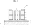
- FIG. 2 is a diagram illustrating another embodiment in which the photonic crystal semiconductor laser device 100 of FIG. 1 is inverted.
- FIG. 3 is a cross-sectional view of a schematic structure of a guide layer 30 of the photonic crystal semiconductor laser device 100 according to an embodiment of the present invention.
- a direction (i.e., z direction) in which layers of the photonic crystal semiconductor laser device 100 are stacked will be referred to as a vertical direction.
- a direction corresponding to a plane (i.e., xy plane) of each layer will be referred to as a horizontal direction.
- these directions are merely examples for describing an embodiment, and the present invention is not limited to the directions.
- the photonic crystal laser device 100 includes an n-type clad layer 21 formed on a first surface of an n-type first substrate 40, a guide layer 30 formed on the n-type clad layer 21 and including an active layer 33, a p-type clad layer 22 formed on the guide layer 30, a p-type contact layer 23 formed on the p-type clad layer 22, a p-type electrode layer 12 formed on the p-type contact layer 23, and an n-type electrode layer 11 contacting at least a portion of the first surface of the n-type first substrate 40 or a second surface opposing the first surface.
- holes H that penetrate the p-type contact layer 23, the p-type clad layer 22, the guide layer 30 including the active layer 33, and the n-type clad layer 21 are formed in the p-type contact layer 23, the p-type clad layer 22, the guide layer 30 including the active layer 33, and the n-type clad layer 21, wherein the holes H form a photonic crystal pattern.
- the photonic crystal semiconductor laser devices 100 illustrated in FIGS. 2 and 3 are in a packaged state in which the photonic crystal semiconductor laser device 100 of FIG. 1 is inverted, and include the same components as the photonic crystal semiconductor laser device 100 of FIG. 1 except for the n-type first substrate 40, and thus the same reference numerals are assigned to the same components.
- the photonic crystal semiconductor laser device 100 of FIG. 1 is the same as the photonic crystal semiconductor laser device 100 of FIG. 2 except that the photonic crystal semiconductor laser device 100 of FIG. 1 is provided with the n-type first substrate 40 in which a hole is not formed, and thus the following descriptions are provided on the basis of the photonic crystal semiconductor laser device 100 of FIG. 2 .
- the photonic crystal laser device 100 includes a p-type electrode layer 12 formed on a substrate 10, a contact layer 23 formed on the p-type electrode layer 12, a p-type clad layer 22 formed on the contact layer 23, a guide layer 30 formed on the p-type clad layer 22 and including an active layer 33, an n-type clad layer 21 formed on the guide layer 30, and an n-type electrode layer 11 contacting at least a portion of an upper surface of the n-type clad layer 21.
- the other portion of the upper surface of the n-type clad layer 21 may contact air.
- holes H penetrating the n-type clad layer 21, the guide layer 30 including the active layer 33, the p-type clad layer 22, and the contact layer 23 are formed.
- the holes H form a two-dimensional photonic crystal pattern on a stack plane (i.e., xy plane).
- the two-dimensional photonic crystal pattern may be, for example, a hexagonal lattice or honeycomb lattice pattern. However, an embodiment is not limited thereto.
- the photonic crystal laser device 100 is capable of electrical oscillation regardless of a shape of the photonic crystal pattern. Therefore, according to an embodiment, the holes H may form a photonic crystal cavity structure including an artificial defect. According to an embodiment, the holes H may also form a random laser structure using a disordered photonic crystal structure. However, an embodiment is not limited thereto.
- the penetration holes H forming a two-dimensional photonic crystal pattern are formed in at least a portion of the laser device 100.
- the n-type electrode layer 11 may be formed on a region in which the penetration holes H are not formed.
- the penetration holes H may be formed in a central region of the laser device 100.
- the holes H may not be formed in an edge region of the laser device 100.
- the n-type electrode layer 11 may be formed on the edge region of the n-type electrode layer 11.
- the n-type electrode 11 may be formed surrounding the holes H that form a photonic crystal pattern.
- the n-type electrode layer 11 may be formed in an annular form when viewed from above an upper surface of the laser device 100.
- this is merely an embodiment, and the region in which the holes H are formed and the shape of the n-type electrode 11 are not limited thereto in various embodiments of the present invention.
- the n-type electrode layer 11 and the p-type electrode layer 12 include metal.
- the n-type clad layer 21, the guide layer 30, the p-type clad layer 22, and the contact layer 23 may be composed of a group III-V compound semiconductor material.
- the contact layer 23, which is a p+ contact layer, may be formed between the p-type electrode layer 12 and the p-type clad layer 22.
- the guide layer 30 includes the active layer 33 therein.
- the active layer 33 may be configured in various forms such as single quantum well or multi-quantum well (MQW).
- light emitted from the active layer 33 may meet a photonic crystal structure, thus forming laser.
- Light electrically emitted from the active layer 33 may form a photonic band structure and optical mode required for laser oscillation, through a two-dimensional crystal pattern formed on an xy plane.
- refractive index of the n-type clad layer 21 and p-type clad layer 22 are lower than a refractive index of the guide layer 30.
- a refractive index difference between the guide layer 30 and the clad layers 21 and 22 may cause formation of a waveguide in the guide layer 30. Accordingly, an optical mode may propagate laterally in the guide layer 30.
- a Bloch mode may be formed in the guide layer 30. That is, in the guide layer 30, an optical mode may be formed according to an optical band structure, and photonic crystal layer may be oscillated through electrical driving.
- the contact layer 23 may facilitate a flow of current between the p-type electrode layer 12 and the p-type clad layer 22 that is a semiconductor material.
- the contact layer 23 may be formed between the p-type electrode layer 12 and the p-type clad layer 22 having low mobility, and a contact layer may be omitted between the n-type electrode 11 and the n-type clad layer 21 having high mobility.
- a contact layer may also be formed between the n-type electrode layer 11 and the n-type clad layer 21 in another embodiment of the present invention.
- the p-type electrode layer 12 may be arranged in a lower portion of the laser device 100, and the n-type electrode layer 11 may be arranged in an upper portion of the laser device 100.
- the p-type electrode layer 12 may be formed in contact with at least a region corresponding to a photonic crystal pattern in the contact layer 23.
- the p-type electrode layer 12 may be formed in contact with an entire lower surface of the contact layer 23.
- the p-type electrode layer 12 may be formed in contact with an upper surface of the substrate 10 and the lower surface of the contact layer 23, and may be formed over an entire stack plane.
- the n-type electrode layer 11 may be formed in contact with only a portion of an upper surface of the n-type clad layer 21.
- the n-type electrode layer 11 may be formed in an edge region of the upper surface of the n-type clad layer 21. In this case, a central region, in which the n-type electrode layer 11 is not formed, of the upper surface of the n-type clad layer 21 may be exposed to air.
- the n-type electrode layer 11 may be arranged on a peripheral portion of the two-dimensional photonic crystal pattern of the laser device 100.
- the p-type electrode layer 12 may be formed facing an entire region of the two-dimensional crystal pattern. This is because electrons may spread laterally in the n-type clad layer 21 since a doping level is high and electron mobility is also high in the n-type clad layer 21, but positive holes cannot spread laterally since a doping level is low and positive hole mobility is also low in the p-type clad layer 22.
- the p-type electrode layer 12 since the mobility is lower in a p-type semiconductor than in an n-type semiconductor, the p-type electrode layer 12 may be arranged in a lower portion of the laser device 100 so that the p-type electrode layer 12 may be formed over an entire stack plane. Furthermore, since the mobility is higher in an n-type semiconductor than in a p-type semiconductor, the n-type electrode layer 11 may be arranged in an upper portion of the laser device 100 so that the n-type electrode layer 11 may be formed on an edge of a stack plane.
- the p-type electrode layer 12 may be formed over an entire stack plane in a lower portion of the laser device 100 and the n-type electrode layer 11 may be formed in an edge region in an upper portion of the laser device 100 so that performance of the laser device 100 may be improved compared to the opposite case.
- the n-type clad layer 21, the guide layer 30, the p-type clad layer 22, and the contact layer 23 may be composed of a group III-V compound semiconductor material.
- the guide layer 30 may be basically formed of a compound represented by indium gallium arsenide phosphide (InGaAsP).
- the n-type clad layer 21 and the p-type clad layer 22 may be basically formed of a compound represented by indium phosphide (InP), and a corresponding dopant may be added thereto.
- An n-type dopant may be added to InP to form the n-type clad layer 21, and a p-type dopant may be added to InP to form the p-type clad layer 22.
- the contact layer 23, which is a p+ contact layer, may be basically formed of a compound represented by indium gallium arsenide (InGaAs) or indium phosphide (InP).
- InGaAs indium gallium arsenide
- InP indium phosphide
- a photonic crystal semiconductor laser device according to various embodiments of the present invention may be composed of various types of compound semiconductor materials.
- the guide layer 30 includes an n-type guide layer 31 contacting the n-type clad layer 21, a p-type guide layer 32 contacting the p-type clad layer 22, and the active layer 33 between the n-type guide layer 31 and the p-type guide layer 32.
- the guide layer 30 may be basically formed of a compound represented by indium gallium arsenide phosphide (InGaAsP).
- the n-type guide layer 31 may be n-doped InGaAsP
- the p-type guide layer 32 may be p-doped InGaAsP.
- a photonic crystal semiconductor laser device may be composed of various types of compound semiconductor materials.
- the active layer 33 may be basically formed of a compound represented by InGaAsP.
- the active layer 33 may have a structure in which a quantum well of InGaAs and a barrier of InGaAsP are alternately repeated.
- FIG.3 illustrates four barrier layers and three quantum well layers therebetween in the active layer 33.
- a current spreading layer 34 may be formed at a position close to the active layer 33.
- the current spreading layer 34 may be n-doped InGaAsP.
- a composition ratio of n-InGaAsP constituting the current spreading layer 34 may be different from a composition ratio of n-InGaAsP constituting the n-type guide layer 31.
- FIG. 4 is a graph G1 obtained by calculating light intensity of the photonic crystal laser device 100 in a vertical direction according to an embodiment of the present invention.
- FIG. 5 is a graph G2 obtained by calculating a refractive index of the photonic crystal layer device 100 in a vertical direction according to an embodiment of the present invention.
- the n-type clad layer 21 is n-InP
- the n-type guide layer 31 is n-InGaAsP
- the p-type guide layer 32 is p-InGaAsP
- the p-type clad layer 22 is p-InP
- the contact layer 23 is p +-InP. It is assumed that four i-InGaAsP barrier layers and three i-InGaAs quantum well layers are alternately stacked in the active layer 33.
- the clad layer 21 and the p-type clad layer 22 have a thickness of about 1 ⁇ m, and the guide layer 30 has a thickness of about 0.4 ⁇ m.
- the present invention is not limited thereto.
- the refractive index of the guide layer 30 is higher than the refractive index of the clad layers 21 and 22. Due to a refractive index difference between the guide layer 30 and the clad layers 21 and 22, the guide layer 30 may serve as a waveguide. Accordingly, an optical mode may propagate in the guide layer 30.
- Graph G1 shows that an optical field is formed around the guide layer 30. Intensity of the optical field is strong in the guide layer 30, and decreases towards an upper portion of the n-type clad layer 21 and towards a lower portion of the p-type clad layer 22. As a result, it is recognized that light intensity approximates to 0 at the upper surface of the n-type clad layer 21 and a lower surface of the p-type clad layer 22. Therefore, according to an embodiment of the present invention, since an optical field does not sense metal of the n-type electrode layer 11 and the p-type electrode layer 12, there may be almost no optical loss, and this is a very import condition for laser oscillation.
- the optical field senses metal, there is no possibility of becoming laser since the optical loss excessively increases. Due to this limitation, the optical loss is excessively large when a metal electrode is directly formed in an existing photonic crystal laser structure by using the guide layer 30 without the clad layers 21 and 22, and thus it is difficult to manufacture a photonic crystal layer capable of electrical injection.
- the optical field is unable to sense metal of the n-type electrode layer 11 and the p-type electrode layer 12 since the n-type clad layer 21 and the p-type clad layer 22 having a sufficient thickness are arranged on and under the guide layer 30.
- the thickness of the n-type clad layer 21 may be set so that the intensity of the optical field approximates to 0 (e.g., equal to or less than specified intensity) at the upper surface of the n-type clad layer 21.
- the thickness of the p-type clad layer 22 may be set so that the intensity of the optical field approximates to 0 (e.g., equal to or less than specified intensity) at the lower surface of the p-type clad layer 22.
- the photonic crystal semiconductor laser device 100 capable of electrical injection regardless of a photonic crystal pattern structure may be provided.
- a photonic band structure and a band-edge mode are satisfactorily formed in a structure of the photonic crystal semiconductor laser device 100 according to an embodiment of the present invention.
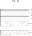
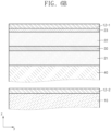
- FIGS. 6A to 6F are diagrams for describing a manufacturing method of the photonic crystal semiconductor laser device 100 according to an embodiment of the present invention.
- a first substrate 40 is a substrate for depositing each layer of a laser device
- a second substrate 10 is a substrate for bonding a manufactured laser device.
- the n-type clad layer 21, the guide layer 30 including the active layer 33, the p-type clad layer 22, and the contact layer 23, which are described above, are sequentially formed and stacked on the first substrate 40.
- the first substrate 40 may be, for example, an indium phosphide (InP) substrate.
- the n-type clad layer 21, the guide layer 30, the p-type clad layer 22, and the contact layer 23 may be deposited in this order on the first substrate 40 through chemical vapor deposition.
- a metal layer 12-1 is formed on the first substrate 40 on which the above-mentioned layers are stacked, and a metal layer 12-2 is formed on the second substrate 10.
- the metal layers 12-1 and 12-2 may be deposited on the first substrate 40 and the second substrate 10. Therefore, on the first substrate 40, the metal layer 12-1 may be formed on the contact layer 23. Thereafter, the metal layers 12-1 and 12-2 may be metal bonded so as to be used as the p-type electrode layer 12.
- the metal layer 12-1 and the metal layer 12-2 are abutted to each other and metal bonded.
- the bonded metal layers 12-1 and 12-2 become the p-type electrode layer 12. Since the second substrate 10 and the first substrate 40 are bonded through the medium of the metal layers 12-1 and 12-2, the first substrate 40 may be stably removed, and a laser device may be mounted on the second substrate 10.
- the first substrate 40 is not necessarily removed.
- the n-type electrode layer 11 described below may also be formed on at least a portion of a surface of the first substrate 40 in which holes are not formed.
- the thickness of the first substrate 40 may be partially removed.
- the first substrate 40 is removed.
- the first substrate 40 may be removed through wet etching.
- the upper surface of the n-type clad layer 21 may be exposed.
- a two-dimensional photonic crystal pattern is formed by forming holes H penetrating the n-type clad layer 21, the guide layer 30, the p-type clad layer 22, and the contact layer 23.
- a two-dimensional photonic crystal pattern may be inscribed through e-beam lithography, and etching may be performed to a depth of the contact layer 23 on the basis of the inscribed pattern.
- the step of forming the holes H penetrating the n-type clad layer 21, the guide layer 30, the p-type clad layer 22, and the contact layer 23 is performed after a metal bonding step, an embodiment is not limited thereto, and the step may be performed before the metal bonding after stacking the n-type clad layer 21, the guide layer 30, the p-type clad layer 22, and the p-type contact layer 23 on the first substrate 40.
- the n-type electrode layer 11 is formed on the upper surface of the n-type clad layer 21 in which the holes H are not formed.
- the n-type electrode layer 11 may be deposited through a lift-off method.
- a pattern for a shape of the n-type electrode layer 11 may be inscribed through e-beam lithography or photolithography, a metal for electrode may be deposited on the inscribed pattern, and the metal may be made to remain only in the pattern through a lift-off method.
- the n-type clad layer 21 may be removed together when the n-type first substrate 40 is removed.
- the n-type electrode layer 11 may be formed on at least a portion of the guide layer 30 in which the holes H are not formed.
- FIG. 7 is a flowchart illustrating a manufacturing method of the photonic crystal semiconductor laser device 100 according to an embodiment of the present invention.
- the n-type clad layer 21, the guide layer 30 including the active layer 33, the p-type clad layer 22, and the contact layer 23 may be sequentially formed and stacked on the first substrate 40.
- the n-type clad layer 21, the guide layer 30, the p-type clad layer 22, and the contact layer 23 may be sequentially deposited on the first substrate 40.
- the first substrate 40 is a substrate for depositing each layer.
- the first metal layer 12-1 may be formed on the contact layer 23 of the first substrate 40, and the second metal layer 12-2 may be formed on the second substrate 10.
- the metal layers 12-1 and 12-2 may be deposited on the first substrate 40 and the second substrate 10.
- the second substrate 10 is a substrate for bonding a manufactured laser device.
- step S3 the first metal layer 12-1 and the second metal layer 12-2 may be abutted to each other and metal bonded.
- the bonded metal layers 12-1 and 12-2 may become the p-type electrode layer 12. Since the second substrate 10 and the first substrate 40 are bonded through the medium of the metal layers 12-1 and 12-2, the first substrate 40 may be stably removed, and a laser device may be mounted on the second substrate 10.
- the first substrate 40 may be removed.
- the first substrate 40 may be removed through wet etching.
- the upper surface of the n-type clad layer 21 may be exposed.
- a two-dimensional photonic crystal pattern may be formed by forming holes H penetrating the n-type clad layer 21, the guide layer 30, the p-type clad layer 22, and the contact layer 23.
- a two-dimensional photonic crystal pattern may be inscribed through e-beam lithography, and etching may be performed to a depth of the contact layer 23 on the basis of the inscribed pattern.
- the n-type electrode layer 11 may be formed on at least a portion of the upper surface of the n-type clad layer 21 in which the holes H are not formed.
- the n-type electrode layer 11 may be deposited using a lift-off method. For example, a pattern for a shape of the n-type electrode layer 11 may be inscribed through e-beam lithography or photolithography, a metal for electrode may be deposited on the inscribed pattern, and the metal may be made to remain only in the pattern through a lift-off method.
- FIGS. 8 to 12 a photonic crystal semiconductor laser device 200 according to another embodiment of the present invention will be described in detail with reference to FIGS. 8 to 12 .
- FIG. 8 is a cross-sectional view of a schematic structure of the photonic crystal semiconductor laser device 200 according to another embodiment of the present invention.
- the photonic crystal laser device 200 according to the other embodiment of the present invention lacks an n-type clad layer compared to the above-mentioned photonic crystal laser device 100.
- the photonic crystal laser device 200 includes a p-type electrode layer 12 formed on a substrate 10, a contact layer 23 formed on the p-type electrode layer 12, a p-type clad layer 22 formed on the contact layer 23, a guide layer 30 formed on the p-type clad layer 22 and including an active layer 33, and an n-type electrode layer 11 contacting at least a portion of an upper surface of the guide layer 30.
- the other portion of the upper surface of the n-type guide layer 30 may contact air.
- holes H penetrating the guide layer 30, the p-type clad layer 22, and the contact layer 23 are formed.
- the holes H form a two-dimensional photonic crystal pattern on a stack plane (i.e., xy plane).
- the holes H may form a two-dimensional photonic crystal pattern, also form a photonic crystal cavity structure including an artificial defect, and also form a random laser structure using a disordered photonic crystal structure.
- the photonic crystal laser device 200 only lacks an n-type clad layer compared to the photonic crystal laser device 100 according to the above-mentioned embodiment, and thus overlapping descriptions of the other components will be omitted.
- a lower surface of the guide layer 30 contacts the p-type clad layer 22, and an upper surface of a region, in which the two-dimensional photonic crystal pattern is formed, of the guide layer 30 contacts air.
- the refractive index of the guide layer 30 is higher than the refractive index of the p-type clad layer 22 and air, a waveguide may be formed in the guide layer 30. Accordingly, an optical mode may propagate laterally in the guide layer 30.
- FIG. 9 is a graph obtained by calculating light intensity of the photonic crystal laser device 200 in a vertical direction according to the embodiment illustrated in FIG. 8 .
- an optical field is asymmetrically formed since the photonic crystal laser device 200 lacks an n-type clad layer and is thus asymmetric in a vertical direction (z direction). Since the refractive index of the p-type clad layer 22 under the guide layer 30 is higher than the refractive index of air above the guide layer 30, the optical field is biased towards a lower portion of the guide layer 30. Since it is desirable to form the active layer 33 in a region in which the optical field is strong, the active layer 33 may be arranged biased towards the p-type clad layer 22 in the guide layer 30 of the photonic crystal laser device 200.
- the p-type guide layer 32 may be formed thinner than the n-type guide layer 31.
- the photonic crystal semiconductor laser device 200 capable of electrical injection regardless of a photonic crystal pattern structure may be provided.
- light emitted from the active layer 33 may meet a photonic crystal structure, thus forming laser.
- Light electrically emitted from the active layer 33 may form a photonic band structure and optical mode required for laser oscillation, through a two-dimensional crystal pattern formed on an xy plane.
- FIG. 10 illustrates a result of simulation of an optical band structure of the photonic crystal laser device 200 according to the embodiment illustrated in FIG. 8
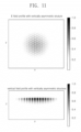
- FIG. 11 illustrates a result of simulation of a field profile of the photonic crystal laser device 200.
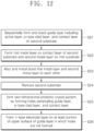
- FIG. 12 is a flowchart illustrating a manufacturing method of the photonic crystal laser device 200 according to the embodiment illustrated in FIG. 8 .
- the guide layer 30 including the active layer 33, the p-type clad layer 22, and the contact layer 23 may be sequentially formed and stacked on a second substrate.
- the guide layer 30, the p-type clad layer 22, and the contact layer 23 may be sequentially deposited on the second substrate.
- the second substrate is a substrate for depositing each layer.
- a first metal layer may be formed on the contact layer 23 of the second substrate, and a second metal layer may be formed on the second substrate 10.
- the metal layers may be deposited on the second substrate and the second substrate 10.
- the second substrate 10 is a substrate for bonding the manufactured laser device 200.
- step S23 the first metal layer and the second metal layer may be abutted to each other and metal bonded.
- the bonded metal layers may become the p-type electrode layer 12. Since the second substrate 10 and the second substrate are bonded through the medium of the metal layers, the second substrate may be stably removed, and a laser device may be mounted on the second substrate 10.
- the second substrate may be removed.
- the second substrate may be removed through wet etching.
- the upper surface of the guide layer 30 may be exposed.
- a two-dimensional photonic crystal pattern may be formed by forming holes H penetrating the guide layer 30, the p-type clad layer 22, and the contact layer 23.
- a two-dimensional photonic crystal pattern may be inscribed through e-beam lithography, and etching may be performed to a depth of the contact layer 23 on the basis of the inscribed pattern.
- the n-type electrode layer 11 may be formed on at least a portion of the upper surface of the guide layer 30 in which the holes H are not formed.
- the n-type electrode layer 11 may be deposited using a lift-off method. For example, a pattern for a shape of the n-type electrode layer 11 may be inscribed through e-beam lithography or photolithography, a metal for electrode may be deposited on the inscribed pattern, and the metal may be made to remain only in the pattern through a lift-off method.
- the photonic crystal semiconductor laser device 200 described through FIGS. 8 to 12 has an asymmetric guide structure in which an n-type clad layer has been removed.
- a manufacturing process is very easy since an etching depth of the holes H may be reduced.
- a photonic band structure is satisfactorily formed also in a structure of the photonic crystal semiconductor laser device 200 having an asymmetric guide structure.
- a photonic crystal semiconductor laser device and a method for manufacturing the same are provided.
Landscapes
- Physics & Mathematics (AREA)
- Condensed Matter Physics & Semiconductors (AREA)
- General Physics & Mathematics (AREA)
- Electromagnetism (AREA)
- Optics & Photonics (AREA)
- Geometry (AREA)
- Semiconductor Lasers (AREA)
Abstract
Description
- The embodiments of the present invention relate to an active optical device, and more particularly, to a semiconductor laser. In detail, the embodiments of the present invention relate to a laser device for electrically driving a photonic crystal laser.
- A photonic crystal refers to a structure in which two materials having different refractive index are periodically arranged on a scale of approximate optical wavelengths. Representative features of a photonic crystal include photonic bandgap, strong nonlinearity, and dispersion characteristics, and a photonic crystal laser is one of optical crystal devices using such characteristics.
- A photonic crystal laser has a laser structure capable of not only providing various functions such as single mode oscillation or laser emission perpendicular to a substrate but also reducing the sizes of existing semiconductor laser devices.
- In the case of a photonic crystal laser using a large difference of refractive index among existing semiconductor lasers, electrical driving is very difficult and restrictive due to structural limitations. In order to produce a photonic crystal laser, micro structures having a very large difference of refractive index are required to be formed as a photonic crystal pattern in a horizontal direction in a device. However, such micro structures make it very difficult to adopt metal electrodes that are essential for electrical driving.
- In detail, since a correlation between a photonic crystal pattern and a metal electrode is very high, there is a structural limitation between an optical waveguide structure and the metal electrode. Due to this limitation, laser oscillation characteristics of existing photonic crystal lasers are very poor, and electrically driven photonic crystal lasers are not yet commercially used.
- The present invention, which has been derived to resolve the above problems, is to provide a photonic crystal semiconductor laser device capable of being electrically driven and a method for manufacturing the same.
- However, this problem is exemplary, and the scope of the present invention is not limited thereto.
- An embodiment of the present invention provides a photonic crystal semiconductor laser device including an n-type clad layer formed on a first surface of an n-type first substrate, a guide layer formed on the n-type clad layer and including an active layer, a p-type clad layer formed on the guide layer, a p-type contact layer formed on the p-type clad layer, a p-type electrode layer formed on the p-type contact layer, and an n-type electrode layer contacting at least a portion of the first surface of the n-type first substrate or a second surface opposing the first surface, wherein holes penetrating the p-type contact layer, the p-type clad layer, the guide layer including the active layer, and the n-type clad layer are formed in the p-type contact layer, the p-type clad layer, the guide layer including the active layer, and the n-type clad layer, and the holes form a photonic crystal pattern.
- According to an embodiment of the present invention configured as described above, a photonic crystal semiconductor laser device can be electrically and stably driven.
- If a photonic crystal semiconductor laser device can be stably driven, the size of a device required for single-mode oscillation can be significantly reduced, and industrial application of a photonic crystal layer can be facilitated.
- The scope of the present invention is not limited to the above effects.
-
-
FIG. 1 is a cross-sectional view of a schematic structure of a photonic crystalsemiconductor laser device 100 according to an embodiment of the present invention. -
FIG. 2 is a diagram illustrating another embodiment in which the photonic crystalsemiconductor laser device 100 ofFIG. 1 is inverted. -
FIG. 3 is a cross-sectional view of a schematic structure of aguide layer 30 of the photonic crystalsemiconductor laser device 100 according to an embodiment of the present invention. -
FIG. 4 is a graph G1 obtained by calculating light intensity of the photoniccrystal laser device 100 in a vertical direction according to an embodiment of the present invention. -
FIG. 5 is a graph G2 obtained by calculating a refractive index of the photoniccrystal layer device 100 in a vertical direction according to an embodiment of the present invention. -
FIGS. 6A to 6F are diagrams for describing a manufacturing method of the photonic crystalsemiconductor laser device 100 according to an embodiment of the present invention. -
FIG. 7 is a flowchart illustrating a manufacturing method of the photonic crystalsemiconductor laser device 100 according to an embodiment of the present invention. -
FIG. 8 is a cross-sectional view of a schematic structure of the photonic crystalsemiconductor laser device 200 according to another embodiment of the present invention. -
FIG. 9 is a graph obtained by calculating light intensity of the photoniccrystal laser device 200 in a vertical direction according to the embodiment illustrated inFIG. 8 . -
FIG. 10 illustrates a result of simulation of an optical band structure of the photoniccrystal laser device 200 according to the embodiment illustrated inFIG. 8 . -
FIG. 11 illustrates a result of simulation of a field profile of the photoniccrystal laser device 200. -
FIG. 12 is a flowchart illustrating a manufacturing method of the photoniccrystal laser device 200 according to the embodiment illustrated inFIG. 8 . - An embodiment of the present invention provides a photonic crystal semiconductor laser device including an n-type clad layer formed on a first surface of an n-type first substrate, a guide layer formed on the n-type clad layer and including an active layer, a p-type clad layer formed on the guide layer, a p-type contact layer formed on the p-type clad layer, a p-type electrode layer formed on the p-type contact layer, and an n-type electrode layer contacting at least a portion of the first surface of the n-type first substrate or a second surface opposing the first surface, wherein holes penetrating the p-type contact layer, the p-type clad layer, the guide layer including the active layer, and the n-type clad layer are formed in the p-type contact layer, the p-type clad layer, the guide layer including the active layer, and the n-type clad layer, and the holes form a photonic crystal pattern.
- In an embodiment of the present invention, refractive index of the p-type clad layer and the n-type clad layer may be lower than a refractive index of the guide layer.
- In an embodiment of the present invention, the holes may form a photonic crystal cavity structure including an artificial defect on a stack plane of the photonic crystal semiconductor laser device.
- In an embodiment of the present invention, the holes may form a random structure using a disordered photonic crystal structure on a stack plane of the photonic crystal semiconductor laser device.
- In an embodiment of the present invention, the holes may be formed in a central region of the photonic crystal semiconductor laser device, and the n-type electrode layer may be formed in an edge region in which the holes are not formed.
- In an embodiment of the present invention, the p-type electrode layer may be formed in contact with a region corresponding to the photonic crystal pattern in the p-type contact layer.
- In an embodiment of the present invention, a thickness of the p-type clad layer may be set so that intensity of an optical field is equal to or less than specified intensity at an upper surface of the p-type clad layer, and a thickness of the n-type clad layer may be set so that the intensity of the optical field is equal to or less than the specified intensity at a lower surface of the n-type clad layer.
- An embodiment of the present invention provides a method for manufacturing a photonic crystal semiconductor laser device, the method including the steps of: sequentially forming and stacking an n-type clad layer, a guide layer including an active layer, a p-type clad layer, and a p-type contact layer on a first surface of an n-type first substrate; forming a photonic crystal pattern by forming holes penetrating the p-type contact layer, the p-type clad layer, the guide layer including the active layer, and the n-type clad layer; forming a first metal layer including a p-type electrode layer on the p-type contact layer and a second metal layer on a second substrate; abutting and metal bonding the first metal layer and the second metal layer to each other; and forming an n-type electrode layer on at least a portion of the first substrate in which the holes are not formed.
- In an embodiment of the present invention, the step of forming the n-type electrode layer may include the steps of: removing a portion of a thickness of the first substrate after the metal bonding step; and forming the n-type electrode layer on at least a portion of a surface of the first substrate having a partially removed thickness.
- An embodiment of the present invention provides a method for manufacturing a photonic crystal semiconductor laser device, the method including the steps of: sequentially forming and stacking an n-type clad layer, a guide layer including an active layer, a p-type clad layer, and a p-type contact layer on a first surface of an n-type first substrate; forming a photonic crystal pattern by forming holes penetrating the p-type contact layer, the p-type clad layer, the guide layer including the active layer, and the n-type clad layer; forming a first metal layer including a p-type electrode layer on the p-type contact layer and a second metal layer on a second substrate; abutting and metal bonding the first metal layer and the second metal layer to each other; completely removing the first substrate after the metal bonding step; and forming an n-type electrode layer on at least a portion of a surface of the n-type clad layer exposed after the first substrate is completely removed.
- An embodiment of the present invention provides a method for manufacturing a photonic crystal semiconductor laser device, the method including the steps of: sequentially forming and stacking an n-type clad layer, a guide layer including an active layer, a p-type clad layer, and a p-type contact layer on an n-type first substrate; forming a first metal layer including a p-type electrode layer on the p-type contact layer and a second metal layer on a second substrate; abutting and metal bonding the first metal layer and the second metal layer to each other; removing the n-type first substrate; forming a photonic crystal pattern by forming holes penetrating the n-type clad layer, the guide layer including the active layer, and the p-type clad layer; and forming an n-type electrode layer on at least a portion of a surface of the n-type clad layer in which the holes are not formed.
- Other aspects, features, and advantages of the present disclosure will become apparent from the detailed description and the claims in conjunction with the accompanying drawings.
- Embodiments of the present invention may be variously modified and may include various examples. However, particular embodiments are exemplarily illustrated in the drawings and will be described in detail. Effects and features of the embodiments of the present invention, and implementation methods thereof will be clarified through following embodiments described with reference to the accompanying drawings. However, the present invention is not limited to the embodiments described below, but may be implemented in various forms.
- Hereinafter, embodiments of the present invention will be described in detail with reference to the accompanying drawings. Like reference numerals refer to like elements throughout, and overlapped descriptions are omitted.
- As used herein, the singular forms "a," "an" and "the" are intended to include the plural forms as well, unless the context clearly indicates otherwise.
- It will be further understood that the terms "comprises" and/or "comprising" used herein specify the presence of stated features or components, but do not preclude the presence or addition of one or more other features or components.
- Sizes of elements in the drawings may be exaggerated for convenience of explanation. In other words, since sizes and thicknesses of components in the drawings are arbitrarily illustrated for convenience of explanation, the following embodiments are not limited thereto.
- In the following embodiments, when a portion such as a region, layer, or component is referred to as being "on" another portion, it can be directly on the other portion or other regions, layers, or components may be interposed therebetween.
- In the following embodiments, when a region, layer, or component is referred to as being connected to each other, the region, layer, or component can be directly connected to each other or can be indirectly connected to each other with other regions, layers, or components interposed therebetween.
-
FIG. 1 is a cross-sectional view of a schematic structure of a photonic crystalsemiconductor laser device 100 according to an embodiment of the present invention, andFIG. 2 is a diagram illustrating another embodiment in which the photonic crystalsemiconductor laser device 100 ofFIG. 1 is inverted.FIG. 3 is a cross-sectional view of a schematic structure of aguide layer 30 of the photonic crystalsemiconductor laser device 100 according to an embodiment of the present invention. - Hereinafter, a direction (i.e., z direction) in which layers of the photonic crystal
semiconductor laser device 100 are stacked will be referred to as a vertical direction. Furthermore, a direction corresponding to a plane (i.e., xy plane) of each layer will be referred to as a horizontal direction. However, these directions are merely examples for describing an embodiment, and the present invention is not limited to the directions. - First, referring to
FIG. 1 , the photoniccrystal laser device 100 according to an embodiment of the present invention includes an n-type cladlayer 21 formed on a first surface of an n-typefirst substrate 40, aguide layer 30 formed on the n-type cladlayer 21 and including anactive layer 33, a p-type cladlayer 22 formed on theguide layer 30, a p-type contact layer 23 formed on the p-type cladlayer 22, a p-type electrode layer 12 formed on the p-type contact layer 23, and an n-type electrode layer 11 contacting at least a portion of the first surface of the n-typefirst substrate 40 or a second surface opposing the first surface. Here, holes H that penetrate the p-type contact layer 23, the p-type cladlayer 22, theguide layer 30 including theactive layer 33, and the n-type cladlayer 21 are formed in the p-type contact layer 23, the p-type cladlayer 22, theguide layer 30 including theactive layer 33, and the n-type cladlayer 21, wherein the holes H form a photonic crystal pattern. - The photonic crystal
semiconductor laser devices 100 illustrated inFIGS. 2 and3 are in a packaged state in which the photonic crystalsemiconductor laser device 100 ofFIG. 1 is inverted, and include the same components as the photonic crystalsemiconductor laser device 100 ofFIG. 1 except for the n-typefirst substrate 40, and thus the same reference numerals are assigned to the same components. The photonic crystalsemiconductor laser device 100 ofFIG. 1 is the same as the photonic crystalsemiconductor laser device 100 ofFIG. 2 except that the photonic crystalsemiconductor laser device 100 ofFIG. 1 is provided with the n-typefirst substrate 40 in which a hole is not formed, and thus the following descriptions are provided on the basis of the photonic crystalsemiconductor laser device 100 ofFIG. 2 . - Referring to
FIGS. 2 and3 , the photoniccrystal laser device 100 according to an embodiment of the present invention includes a p-type electrode layer 12 formed on asubstrate 10, acontact layer 23 formed on the p-type electrode layer 12, a p-type cladlayer 22 formed on thecontact layer 23, aguide layer 30 formed on the p-type cladlayer 22 and including anactive layer 33, an n-type cladlayer 21 formed on theguide layer 30, and an n-type electrode layer 11 contacting at least a portion of an upper surface of the n-type cladlayer 21. The other portion of the upper surface of the n-type cladlayer 21 may contact air. - In the photonic
crystal laser device 100 according to an embodiment of the present invention, holes H penetrating the n-type cladlayer 21, theguide layer 30 including theactive layer 33, the p-type cladlayer 22, and thecontact layer 23 are formed. The holes H form a two-dimensional photonic crystal pattern on a stack plane (i.e., xy plane). The two-dimensional photonic crystal pattern may be, for example, a hexagonal lattice or honeycomb lattice pattern. However, an embodiment is not limited thereto. - The photonic
crystal laser device 100 according to an embodiment of the present invention is capable of electrical oscillation regardless of a shape of the photonic crystal pattern. Therefore, according to an embodiment, the holes H may form a photonic crystal cavity structure including an artificial defect. According to an embodiment, the holes H may also form a random laser structure using a disordered photonic crystal structure. However, an embodiment is not limited thereto. - The penetration holes H forming a two-dimensional photonic crystal pattern are formed in at least a portion of the
laser device 100. The n-type electrode layer 11 may be formed on a region in which the penetration holes H are not formed. - According to an embodiment, the penetration holes H may be formed in a central region of the
laser device 100. The holes H may not be formed in an edge region of thelaser device 100. For example, the n-type electrode layer 11 may be formed on the edge region of the n-type electrode layer 11. - For example, the n-
type electrode 11 may be formed surrounding the holes H that form a photonic crystal pattern. For example, the n-type electrode layer 11 may be formed in an annular form when viewed from above an upper surface of thelaser device 100. However, this is merely an embodiment, and the region in which the holes H are formed and the shape of the n-type electrode 11 are not limited thereto in various embodiments of the present invention. - The n-
type electrode layer 11 and the p-type electrode layer 12 include metal. The n-type cladlayer 21, theguide layer 30, the p-type cladlayer 22, and thecontact layer 23 may be composed of a group III-V compound semiconductor material. Thecontact layer 23, which is a p+ contact layer, may be formed between the p-type electrode layer 12 and the p-type cladlayer 22. - The
guide layer 30 includes theactive layer 33 therein. Theactive layer 33 may be configured in various forms such as single quantum well or multi-quantum well (MQW). - When a bias is applied through the n-
type electrode layer 11 connected to the n-type cladlayer 21 and the p-type electrode layer 12 connected to the p-type cladlayer 22, electrons and holes having charges are recombined in theactive layer 33, thereby generating light. In detail, electrons may move in a direction from the n-type electrode layer 11 to the p-type electrode layer 12. When a voltage is applied between the electrode layers 11 and 12, a p-n junction diode is formed, and light is emitted from theactive layer 33. - According to embodiments of the present invention, light emitted from the
active layer 33 may meet a photonic crystal structure, thus forming laser. Light electrically emitted from theactive layer 33 may form a photonic band structure and optical mode required for laser oscillation, through a two-dimensional crystal pattern formed on an xy plane. - In an embodiment of the present invention, refractive index of the n-type clad
layer 21 and p-type cladlayer 22 are lower than a refractive index of theguide layer 30. A refractive index difference between theguide layer 30 and theclad layers guide layer 30. Accordingly, an optical mode may propagate laterally in theguide layer 30. - Due to the deep holes H forming a two-dimensional photonic crystal pattern, a Bloch mode may be formed in the
guide layer 30. That is, in theguide layer 30, an optical mode may be formed according to an optical band structure, and photonic crystal layer may be oscillated through electrical driving. - The
contact layer 23, which is a p+ contact layer, is a layer with an increased doping level. Thecontact layer 23 may facilitate a flow of current between the p-type electrode layer 12 and the p-type cladlayer 22 that is a semiconductor material. According to an embodiment, thecontact layer 23 may be formed between the p-type electrode layer 12 and the p-type cladlayer 22 having low mobility, and a contact layer may be omitted between the n-type electrode 11 and the n-type cladlayer 21 having high mobility. However, an embodiment is not limited thereto, and a contact layer may also be formed between the n-type electrode layer 11 and the n-type cladlayer 21 in another embodiment of the present invention. - In an embodiment of the present invention, the p-
type electrode layer 12 may be arranged in a lower portion of thelaser device 100, and the n-type electrode layer 11 may be arranged in an upper portion of thelaser device 100. - For example, the p-
type electrode layer 12 may be formed in contact with at least a region corresponding to a photonic crystal pattern in thecontact layer 23. As an embodiment, the p-type electrode layer 12 may be formed in contact with an entire lower surface of thecontact layer 23. The p-type electrode layer 12 may be formed in contact with an upper surface of thesubstrate 10 and the lower surface of thecontact layer 23, and may be formed over an entire stack plane. - The n-
type electrode layer 11 may be formed in contact with only a portion of an upper surface of the n-type cladlayer 21. For example, the n-type electrode layer 11 may be formed in an edge region of the upper surface of the n-type cladlayer 21. In this case, a central region, in which the n-type electrode layer 11 is not formed, of the upper surface of the n-type cladlayer 21 may be exposed to air. - As described above, according to an embodiment of the present invention, the n-
type electrode layer 11 may be arranged on a peripheral portion of the two-dimensional photonic crystal pattern of thelaser device 100. On the contrary, the p-type electrode layer 12 may be formed facing an entire region of the two-dimensional crystal pattern. This is because electrons may spread laterally in the n-type cladlayer 21 since a doping level is high and electron mobility is also high in the n-type cladlayer 21, but positive holes cannot spread laterally since a doping level is low and positive hole mobility is also low in the p-type cladlayer 22. - According to an embodiment of the present invention, since the mobility is lower in a p-type semiconductor than in an n-type semiconductor, the p-
type electrode layer 12 may be arranged in a lower portion of thelaser device 100 so that the p-type electrode layer 12 may be formed over an entire stack plane. Furthermore, since the mobility is higher in an n-type semiconductor than in a p-type semiconductor, the n-type electrode layer 11 may be arranged in an upper portion of thelaser device 100 so that the n-type electrode layer 11 may be formed on an edge of a stack plane. - In an embodiment of the present invention, the p-
type electrode layer 12 may be formed over an entire stack plane in a lower portion of thelaser device 100 and the n-type electrode layer 11 may be formed in an edge region in an upper portion of thelaser device 100 so that performance of thelaser device 100 may be improved compared to the opposite case. - The n-type clad
layer 21, theguide layer 30, the p-type cladlayer 22, and thecontact layer 23 may be composed of a group III-V compound semiconductor material. - According to an embodiment, the
guide layer 30 may be basically formed of a compound represented by indium gallium arsenide phosphide (InGaAsP). According to an embodiment, the n-type cladlayer 21 and the p-type cladlayer 22 may be basically formed of a compound represented by indium phosphide (InP), and a corresponding dopant may be added thereto. An n-type dopant may be added to InP to form the n-type cladlayer 21, and a p-type dopant may be added to InP to form the p-type cladlayer 22. Thecontact layer 23, which is a p+ contact layer, may be basically formed of a compound represented by indium gallium arsenide (InGaAs) or indium phosphide (InP). However, this is merely an embodiment, and the present invention is not limited thereto. A photonic crystal semiconductor laser device according to various embodiments of the present invention may be composed of various types of compound semiconductor materials. - Referring to
FIG. 3 , theguide layer 30 includes an n-type guide layer 31 contacting the n-type cladlayer 21, a p-type guide layer 32 contacting the p-type cladlayer 22, and theactive layer 33 between the n-type guide layer 31 and the p-type guide layer 32. - According to an embodiment, the
guide layer 30 may be basically formed of a compound represented by indium gallium arsenide phosphide (InGaAsP). For example, the n-type guide layer 31 may be n-doped InGaAsP, and the p-type guide layer 32 may be p-doped InGaAsP. However, this is merely an embodiment, and the present invention is not limited thereto. A photonic crystal semiconductor laser device according to various embodiments of the present invention may be composed of various types of compound semiconductor materials. - According to an embodiment, the
active layer 33 may be basically formed of a compound represented by InGaAsP. For example, theactive layer 33 may have a structure in which a quantum well of InGaAs and a barrier of InGaAsP are alternately repeated. As an example,FIG.3 illustrates four barrier layers and three quantum well layers therebetween in theactive layer 33. - In the n-
type guide layer 31, a current spreadinglayer 34 may be formed at a position close to theactive layer 33. In an embodiment, the current spreadinglayer 34 may be n-doped InGaAsP. For example, a composition ratio of n-InGaAsP constituting the current spreadinglayer 34 may be different from a composition ratio of n-InGaAsP constituting the n-type guide layer 31. -
FIG. 4 is a graph G1 obtained by calculating light intensity of the photoniccrystal laser device 100 in a vertical direction according to an embodiment of the present invention.FIG. 5 is a graph G2 obtained by calculating a refractive index of the photoniccrystal layer device 100 in a vertical direction according to an embodiment of the present invention. - In graphs G1 and G2, it is assumed that the n-type clad
layer 21 is n-InP, the n-type guide layer 31 is n-InGaAsP, the p-type guide layer 32 is p-InGaAsP, the p-type cladlayer 22 is p-InP, and thecontact layer 23 is p +-InP. It is assumed that four i-InGaAsP barrier layers and three i-InGaAs quantum well layers are alternately stacked in theactive layer 33. (i represents an undoped state.) Furthermore, it is assumed that theclad layer 21 and the p-type cladlayer 22 have a thickness of about 1 µm, and theguide layer 30 has a thickness of about 0.4 µm. However, it is a matter of course that the present invention is not limited thereto. - Referring to graph G2, the refractive index of the
guide layer 30 is higher than the refractive index of theclad layers guide layer 30 and theclad layers guide layer 30 may serve as a waveguide. Accordingly, an optical mode may propagate in theguide layer 30. - Graph G1 shows that an optical field is formed around the
guide layer 30. Intensity of the optical field is strong in theguide layer 30, and decreases towards an upper portion of the n-type cladlayer 21 and towards a lower portion of the p-type cladlayer 22. As a result, it is recognized that light intensity approximates to 0 at the upper surface of the n-type cladlayer 21 and a lower surface of the p-type cladlayer 22. Therefore, according to an embodiment of the present invention, since an optical field does not sense metal of the n-type electrode layer 11 and the p-type electrode layer 12, there may be almost no optical loss, and this is a very import condition for laser oscillation. - If the optical field senses metal, there is no possibility of becoming laser since the optical loss excessively increases. Due to this limitation, the optical loss is excessively large when a metal electrode is directly formed in an existing photonic crystal laser structure by using the
guide layer 30 without theclad layers - However, according to an embodiment of the present invention, the optical field is unable to sense metal of the n-
type electrode layer 11 and the p-type electrode layer 12 since the n-type cladlayer 21 and the p-type cladlayer 22 having a sufficient thickness are arranged on and under theguide layer 30. For example, the thickness of the n-type cladlayer 21 may be set so that the intensity of the optical field approximates to 0 (e.g., equal to or less than specified intensity) at the upper surface of the n-type cladlayer 21. The thickness of the p-type cladlayer 22 may be set so that the intensity of the optical field approximates to 0 (e.g., equal to or less than specified intensity) at the lower surface of the p-type cladlayer 22. - Therefore, according to an embodiment of the present invention, the photonic crystal
semiconductor laser device 100 capable of electrical injection regardless of a photonic crystal pattern structure may be provided. Although not illustrated, it was identified that a photonic band structure and a band-edge mode are satisfactorily formed in a structure of the photonic crystalsemiconductor laser device 100 according to an embodiment of the present invention. -
FIGS. 6A to 6F are diagrams for describing a manufacturing method of the photonic crystalsemiconductor laser device 100 according to an embodiment of the present invention. - First, two substrates or wafers are prepared in
FIG. 6A . Afirst substrate 40 is a substrate for depositing each layer of a laser device, and asecond substrate 10 is a substrate for bonding a manufactured laser device. The n-type cladlayer 21, theguide layer 30 including theactive layer 33, the p-type cladlayer 22, and thecontact layer 23, which are described above, are sequentially formed and stacked on thefirst substrate 40. Thefirst substrate 40 may be, for example, an indium phosphide (InP) substrate. For example, the n-type cladlayer 21, theguide layer 30, the p-type cladlayer 22, and thecontact layer 23 may be deposited in this order on thefirst substrate 40 through chemical vapor deposition. - Next, in
FIG. 6B , a metal layer 12-1 is formed on thefirst substrate 40 on which the above-mentioned layers are stacked, and a metal layer 12-2 is formed on thesecond substrate 10. For example, the metal layers 12-1 and 12-2 may be deposited on thefirst substrate 40 and thesecond substrate 10. Therefore, on thefirst substrate 40, the metal layer 12-1 may be formed on thecontact layer 23. Thereafter, the metal layers 12-1 and 12-2 may be metal bonded so as to be used as the p-type electrode layer 12. - Next, in
FIG. 6C , the metal layer 12-1 and the metal layer 12-2 are abutted to each other and metal bonded. The bonded metal layers 12-1 and 12-2 become the p-type electrode layer 12. Since thesecond substrate 10 and thefirst substrate 40 are bonded through the medium of the metal layers 12-1 and 12-2, thefirst substrate 40 may be stably removed, and a laser device may be mounted on thesecond substrate 10. - As another embodiment, the
first substrate 40 is not necessarily removed. The n-type electrode layer 11 described below may also be formed on at least a portion of a surface of thefirst substrate 40 in which holes are not formed. Here, the thickness of thefirst substrate 40 may be partially removed. - Next, in
FIG. 6D , thefirst substrate 40 is removed. For example, thefirst substrate 40 may be removed through wet etching. As a result, the upper surface of the n-type cladlayer 21 may be exposed. - Next, in
FIG. 6E , a two-dimensional photonic crystal pattern is formed by forming holes H penetrating the n-type cladlayer 21, theguide layer 30, the p-type cladlayer 22, and thecontact layer 23. For example, a two-dimensional photonic crystal pattern may be inscribed through e-beam lithography, and etching may be performed to a depth of thecontact layer 23 on the basis of the inscribed pattern. - Here, although it has been described that the step of forming the holes H penetrating the n-type clad
layer 21, theguide layer 30, the p-type cladlayer 22, and thecontact layer 23 is performed after a metal bonding step, an embodiment is not limited thereto, and the step may be performed before the metal bonding after stacking the n-type cladlayer 21, theguide layer 30, the p-type cladlayer 22, and the p-type contact layer 23 on thefirst substrate 40. - Next, in
FIG. 6F , the n-type electrode layer 11 is formed on the upper surface of the n-type cladlayer 21 in which the holes H are not formed. According to an embodiment, the n-type electrode layer 11 may be deposited through a lift-off method. For example, a pattern for a shape of the n-type electrode layer 11 may be inscribed through e-beam lithography or photolithography, a metal for electrode may be deposited on the inscribed pattern, and the metal may be made to remain only in the pattern through a lift-off method. - As another example, the n-type clad
layer 21 may be removed together when the n-typefirst substrate 40 is removed. In this case, the n-type electrode layer 11 may be formed on at least a portion of theguide layer 30 in which the holes H are not formed. -
FIG. 7 is a flowchart illustrating a manufacturing method of the photonic crystalsemiconductor laser device 100 according to an embodiment of the present invention. - Referring to
FIG. 7 , in step S1, the n-type cladlayer 21, theguide layer 30 including theactive layer 33, the p-type cladlayer 22, and thecontact layer 23 may be sequentially formed and stacked on thefirst substrate 40. For example, the n-type cladlayer 21, theguide layer 30, the p-type cladlayer 22, and thecontact layer 23 may be sequentially deposited on thefirst substrate 40. Thefirst substrate 40 is a substrate for depositing each layer. - In step S2, the first metal layer 12-1 may be formed on the
contact layer 23 of thefirst substrate 40, and the second metal layer 12-2 may be formed on thesecond substrate 10. For example, the metal layers 12-1 and 12-2 may be deposited on thefirst substrate 40 and thesecond substrate 10. Thesecond substrate 10 is a substrate for bonding a manufactured laser device. - In step S3, the first metal layer 12-1 and the second metal layer 12-2 may be abutted to each other and metal bonded. The bonded metal layers 12-1 and 12-2 may become the p-
type electrode layer 12. Since thesecond substrate 10 and thefirst substrate 40 are bonded through the medium of the metal layers 12-1 and 12-2, thefirst substrate 40 may be stably removed, and a laser device may be mounted on thesecond substrate 10. - In step S4, the
first substrate 40 may be removed. For example, thefirst substrate 40 may be removed through wet etching. As a result, the upper surface of the n-type cladlayer 21 may be exposed. - In step S5, a two-dimensional photonic crystal pattern may be formed by forming holes H penetrating the n-type clad
layer 21, theguide layer 30, the p-type cladlayer 22, and thecontact layer 23. For example, a two-dimensional photonic crystal pattern may be inscribed through e-beam lithography, and etching may be performed to a depth of thecontact layer 23 on the basis of the inscribed pattern. - In step S6, the n-
type electrode layer 11 may be formed on at least a portion of the upper surface of the n-type cladlayer 21 in which the holes H are not formed. According to an embodiment, the n-type electrode layer 11 may be deposited using a lift-off method. For example, a pattern for a shape of the n-type electrode layer 11 may be inscribed through e-beam lithography or photolithography, a metal for electrode may be deposited on the inscribed pattern, and the metal may be made to remain only in the pattern through a lift-off method. - Hereinafter, a photonic crystal
semiconductor laser device 200 according to another embodiment of the present invention will be described in detail with reference toFIGS. 8 to 12 . -
FIG. 8 is a cross-sectional view of a schematic structure of the photonic crystalsemiconductor laser device 200 according to another embodiment of the present invention. The photoniccrystal laser device 200 according to the other embodiment of the present invention lacks an n-type clad layer compared to the above-mentioned photoniccrystal laser device 100. - That is, the photonic
crystal laser device 200 includes a p-type electrode layer 12 formed on asubstrate 10, acontact layer 23 formed on the p-type electrode layer 12, a p-type cladlayer 22 formed on thecontact layer 23, aguide layer 30 formed on the p-type cladlayer 22 and including anactive layer 33, and an n-type electrode layer 11 contacting at least a portion of an upper surface of theguide layer 30. The other portion of the upper surface of the n-type guide layer 30 may contact air. - In the photonic
crystal laser device 200, holes H penetrating theguide layer 30, the p-type cladlayer 22, and thecontact layer 23 are formed. The holes H form a two-dimensional photonic crystal pattern on a stack plane (i.e., xy plane). The holes H may form a two-dimensional photonic crystal pattern, also form a photonic crystal cavity structure including an artificial defect, and also form a random laser structure using a disordered photonic crystal structure. - The photonic
crystal laser device 200 only lacks an n-type clad layer compared to the photoniccrystal laser device 100 according to the above-mentioned embodiment, and thus overlapping descriptions of the other components will be omitted. - In the photonic
crystal laser device 200, a lower surface of theguide layer 30 contacts the p-type cladlayer 22, and an upper surface of a region, in which the two-dimensional photonic crystal pattern is formed, of theguide layer 30 contacts air. Here, since the refractive index of theguide layer 30 is higher than the refractive index of the p-type cladlayer 22 and air, a waveguide may be formed in theguide layer 30. Accordingly, an optical mode may propagate laterally in theguide layer 30. -
FIG. 9 is a graph obtained by calculating light intensity of the photoniccrystal laser device 200 in a vertical direction according to the embodiment illustrated inFIG. 8 . - It is recognized that an optical field is asymmetrically formed since the photonic
crystal laser device 200 lacks an n-type clad layer and is thus asymmetric in a vertical direction (z direction). Since the refractive index of the p-type cladlayer 22 under theguide layer 30 is higher than the refractive index of air above theguide layer 30, the optical field is biased towards a lower portion of theguide layer 30. Since it is desirable to form theactive layer 33 in a region in which the optical field is strong, theactive layer 33 may be arranged biased towards the p-type cladlayer 22 in theguide layer 30 of the photoniccrystal laser device 200. - That is, in the
guide layer 30 of the photoniccrystal laser device 200, the p-type guide layer 32 may be formed thinner than the n-type guide layer 31. - It is recognized that light intensity approximates to 0 at the upper surface of the
guide layer 30 and the lower surface of the p-type cladlayer 22 in the photoniccrystal laser device 200. Therefore, according to an embodiment of the present invention, since an optical field does not sense metal of the n-type electrode layer 11 and the p-type electrode layer 12, there may be almost no optical loss, and this is a very import condition for laser oscillation. - Therefore, according to an embodiment of the present invention, the photonic crystal
semiconductor laser device 200 capable of electrical injection regardless of a photonic crystal pattern structure may be provided. - According to embodiments of the present invention, light emitted from the
active layer 33 may meet a photonic crystal structure, thus forming laser. Light electrically emitted from theactive layer 33 may form a photonic band structure and optical mode required for laser oscillation, through a two-dimensional crystal pattern formed on an xy plane. - It was identified that a photonic band structure and a band-edge mode are satisfactorily formed also in the asymmetric photonic
crystal laser device 200 according to an embodiment of the present invention. -
FIG. 10 illustrates a result of simulation of an optical band structure of the photoniccrystal laser device 200 according to the embodiment illustrated inFIG. 8 , andFIG. 11 illustrates a result of simulation of a field profile of the photoniccrystal laser device 200. -
FIG. 12 is a flowchart illustrating a manufacturing method of the photoniccrystal laser device 200 according to the embodiment illustrated inFIG. 8 . - Referring to
FIG. 12 , in step S21, theguide layer 30 including theactive layer 33, the p-type cladlayer 22, and thecontact layer 23 may be sequentially formed and stacked on a second substrate. For example, theguide layer 30, the p-type cladlayer 22, and thecontact layer 23 may be sequentially deposited on the second substrate. The second substrate is a substrate for depositing each layer. - In step S22, a first metal layer may be formed on the
contact layer 23 of the second substrate, and a second metal layer may be formed on thesecond substrate 10. For example, the metal layers may be deposited on the second substrate and thesecond substrate 10. Thesecond substrate 10 is a substrate for bonding the manufacturedlaser device 200. - In step S23, the first metal layer and the second metal layer may be abutted to each other and metal bonded. The bonded metal layers may become the p-
type electrode layer 12. Since thesecond substrate 10 and the second substrate are bonded through the medium of the metal layers, the second substrate may be stably removed, and a laser device may be mounted on thesecond substrate 10. - In step S24, the second substrate may be removed. For example, the second substrate may be removed through wet etching. As a result, the upper surface of the
guide layer 30 may be exposed. - In step S25, a two-dimensional photonic crystal pattern may be formed by forming holes H penetrating the
guide layer 30, the p-type cladlayer 22, and thecontact layer 23. For example, a two-dimensional photonic crystal pattern may be inscribed through e-beam lithography, and etching may be performed to a depth of thecontact layer 23 on the basis of the inscribed pattern. - In step S26, the n-
type electrode layer 11 may be formed on at least a portion of the upper surface of theguide layer 30 in which the holes H are not formed. According to an embodiment, the n-type electrode layer 11 may be deposited using a lift-off method. For example, a pattern for a shape of the n-type electrode layer 11 may be inscribed through e-beam lithography or photolithography, a metal for electrode may be deposited on the inscribed pattern, and the metal may be made to remain only in the pattern through a lift-off method. - The photonic crystal
semiconductor laser device 200 described throughFIGS. 8 to 12 has an asymmetric guide structure in which an n-type clad layer has been removed. In the case of such an asymmetric guide structure, a manufacturing process is very easy since an etching depth of the holes H may be reduced. Furthermore, it was identified that a photonic band structure is satisfactorily formed also in a structure of the photonic crystalsemiconductor laser device 200 having an asymmetric guide structure. - Although the the present invention has been described with reference to the embodiments illustrated in the drawings, the embodiments are merely examples and it should be understood that other various modifications and equivalent embodiments could be made by those skilled in the art. Therefore, the technical protection scope of the present invention should be determined based on the technical concept of the following claims.
- According to an embodiment of the present invention, a photonic crystal semiconductor laser device and a method for manufacturing the same are provided.
Claims (11)
- A photonic crystal semiconductor laser device comprising:an n-type clad layer formed on a first surface of an n-type first substrate;a guide layer formed on the n-type clad layer and including an active layer;a p-type clad layer formed on the guide layer;a p-type contact layer formed on the p-type clad layer;a p-type electrode layer formed on the p-type contact layer; andan n-type electrode layer contacting at least a portion of the first surface of the n-type first substrate or a second surface opposing the first surface,wherein holes penetrating the p-type contact layer, the p-type clad layer, the guide layer including the active layer, and the n-type clad layer are formed in the p-type contact layer, the p-type clad layer, the guide layer including the active layer, and the n-type clad layer, andthe holes form a photonic crystal pattern.
- The photonic crystal semiconductor laser device of claim 1, wherein refractive index of the p-type clad layer and the n-type clad layer are lower than a refractive index of the guide layer.
- The photonic crystal semiconductor laser device of claim 1, wherein the holes form a photonic crystal cavity structure including an artificial defect on a stack plane of the photonic crystal semiconductor laser device.
- The photonic crystal semiconductor laser device of claim 1, wherein the holes form a random structure using a disordered photonic crystal structure on a stack plane of the photonic crystal semiconductor laser device.
- The photonic crystal semiconductor laser device of claim 1, wherein the holes are formed in a central region of the photonic crystal semiconductor laser device, and the n-type electrode layer is formed in an edge region in which the holes are not formed.
- The photonic crystal semiconductor laser device of claim 1, wherein the p-type electrode layer is formed in contact with a region corresponding to the photonic crystal pattern in the p-type contact layer.
- The photonic crystal semiconductor laser device of claim 1, wherein a thickness of the p-type clad layer is set so that intensity of an optical field is equal to or less than specified intensity at an upper surface of the p-type clad layer, and a thickness of the n-type clad layer is set so that the intensity of the optical field is equal to or less than the specified intensity at a lower surface of the n-type clad layer.
- A method for manufacturing a photonic crystal semiconductor laser device, the method comprising the steps of:sequentially forming and stacking an n-type clad layer, a guide layer including an active layer, a p-type clad layer, and a p-type contact layer on a first surface of an n-type first substrate;forming a photonic crystal pattern by forming holes penetrating the p-type contact layer, the p-type clad layer, the guide layer including the active layer, and the n-type clad layer;forming a first metal layer including a p-type electrode layer on the p-type contact layer and a second metal layer on a second substrate;abutting and metal bonding the first metal layer and the second metal layer to each other; andforming an n-type electrode layer on at least a portion of the first substrate in which the holes are not formed.
- The method of claim 8, wherein the step of forming the n-type electrode layer comprises the steps of:removing a portion of a thickness of the first substrate after the metal bonding step; andforming the n-type electrode layer on at least a portion of a surface of the first substrate having a partially removed thickness.
- A method for manufacturing a photonic crystal semiconductor laser device, the method comprising the steps of:sequentially forming and stacking an n-type clad layer, a guide layer including an active layer, a p-type clad layer, and a p-type contact layer on a first surface of an n-type first substrate;forming a photonic crystal pattern by forming holes penetrating the p-type contact layer, the p-type clad layer, the guide layer including the active layer, and the n-type clad layer;forming a first metal layer including a p-type electrode layer on the p-type contact layer and a second metal layer on a second substrate;abutting and metal bonding the first metal layer and the second metal layer to each other;completely removing the first substrate after the metal bonding step; andforming an n-type electrode layer on at least a portion of a surface of the n-type clad layer exposed after the first substrate is completely removed.
- A method for manufacturing a photonic crystal semiconductor laser device, the method comprising the steps of:sequentially forming and stacking an n-type clad layer, a guide layer including an active layer, a p-type clad layer, and a p-type contact layer on an n-type first substrate;forming a first metal layer including a p-type electrode layer on the p-type contact layer and a second metal layer on a second substrate;abutting and metal bonding the first metal layer and the second metal layer to each other;removing the n-type first substrate;forming a photonic crystal pattern by forming holes penetrating the n-type clad layer, the guide layer including the active layer, and the p-type clad layer; andforming an n-type electrode layer on at least a portion of a surface of the n-type clad layer in which the holes are not formed.
Applications Claiming Priority (2)
| Application Number | Priority Date | Filing Date | Title |
|---|---|---|---|
| KR1020210034614A KR102452494B1 (en) | 2021-03-17 | 2021-03-17 | Photonic crystal semiconductor laser device and its manufacturing method |
| PCT/KR2022/003738 WO2022197115A1 (en) | 2021-03-17 | 2022-03-17 | Photonic crystal semiconductor laser device and method for manufacturing same |
Publications (2)
| Publication Number | Publication Date |
|---|---|
| EP4311045A1 true EP4311045A1 (en) | 2024-01-24 |
| EP4311045A4 EP4311045A4 (en) | 2025-04-02 |
Family
ID=83321509
Family Applications (1)
| Application Number | Title | Priority Date | Filing Date |
|---|---|---|---|
| EP22771781.6A Pending EP4311045A4 (en) | 2021-03-17 | 2022-03-17 | Photonic crystal semiconductor laser device and method for manufacturing same |
Country Status (5)
| Country | Link |
|---|---|
| US (1) | US20240170918A1 (en) |
| EP (1) | EP4311045A4 (en) |
| KR (1) | KR102452494B1 (en) |
| CN (1) | CN117296218A (en) |
| WO (1) | WO2022197115A1 (en) |
Families Citing this family (1)
| Publication number | Priority date | Publication date | Assignee | Title |
|---|---|---|---|---|
| KR102868728B1 (en) * | 2022-12-27 | 2025-10-17 | (재)한국나노기술원 | Thin-film type InGaAs laser cell manufacturing method and thin-film type InGaAs laser cell |
Family Cites Families (12)
| Publication number | Priority date | Publication date | Assignee | Title |
|---|---|---|---|---|
| CN1236344C (en) * | 2002-12-31 | 2006-01-11 | 中国科学院物理研究所 | Preparation method of tridimensional controllable defect state photon crystal |
| KR20060039704A (en) * | 2004-11-03 | 2006-05-09 | 삼성전기주식회사 | Multi-wavelength laser diode and manufacturing method thereof |
| JP5055717B2 (en) * | 2005-06-20 | 2012-10-24 | 富士ゼロックス株式会社 | Surface emitting semiconductor laser |
| JP4720834B2 (en) * | 2008-02-25 | 2011-07-13 | 住友電気工業株式会社 | Group III nitride semiconductor laser |
| CN101667715B (en) * | 2008-09-03 | 2010-10-27 | 中国科学院半导体研究所 | A single-mode high-power vertical-cavity surface-emitting laser and its manufacturing method |
| GB0902569D0 (en) * | 2009-02-16 | 2009-04-01 | Univ Southampton | An optical device |
| US8611382B2 (en) * | 2009-02-25 | 2013-12-17 | Koninklijke Philips N.V. | Output power stabilization for laser diodes using the photon-cooling dependent laser voltage |
| JP5363578B2 (en) * | 2009-09-01 | 2013-12-11 | 日本電信電話株式会社 | Photonic crystal device |
| US8471352B2 (en) * | 2010-04-05 | 2013-06-25 | The Board Of Trustees Of The Leland Stanford Junior University | Practical electrically pumped photonic crystal nanocavity |
| CN102201648B (en) * | 2011-04-14 | 2012-05-02 | 中国科学院半导体研究所 | FP Cavity Enhanced Electrically Injected Photonic Crystal Band Edge Surface Emitting Laser |
| CN102299243A (en) * | 2011-09-14 | 2011-12-28 | 青岛理工大学 | Thin-film flip-chip photonic crystal LED chip and manufacturing method thereof |
| KR20140130936A (en) * | 2013-05-02 | 2014-11-12 | 한국전자통신연구원 | Ridge waveguide semiconductor laser diode and method for manufacturing the same |
-
2021
- 2021-03-17 KR KR1020210034614A patent/KR102452494B1/en active Active
-
2022
- 2022-03-17 CN CN202280034790.8A patent/CN117296218A/en active Pending
- 2022-03-17 US US18/550,592 patent/US20240170918A1/en active Pending
- 2022-03-17 EP EP22771781.6A patent/EP4311045A4/en active Pending
- 2022-03-17 WO PCT/KR2022/003738 patent/WO2022197115A1/en not_active Ceased
Also Published As
| Publication number | Publication date |
|---|---|
| EP4311045A4 (en) | 2025-04-02 |
| KR102452494B1 (en) | 2022-10-07 |
| KR20220129823A (en) | 2022-09-26 |
| US20240170918A1 (en) | 2024-05-23 |
| WO2022197115A1 (en) | 2022-09-22 |
| CN117296218A (en) | 2023-12-26 |
Similar Documents
| Publication | Publication Date | Title |
|---|---|---|
| US8068526B2 (en) | Semiconductor optical device | |
| US8003995B2 (en) | Semiconductor optical device with suppressed double injection phenomenon | |
| JP4158383B2 (en) | Semiconductor optical integrated device | |
| US5801071A (en) | Method for producing semiconductor laser diode | |
| JP2018152430A (en) | Semiconductor laser | |
| US20030042479A1 (en) | Optical semiconductor devices and fabrication method | |
| CN103125054A (en) | Photoelectric device | |
| TWI748717B (en) | Semiconductor device and manufacturing method thereof | |
| US20240170918A1 (en) | Photonic crystal semiconductor laser device and method for manufacturing same | |
| US6931041B2 (en) | Integrated semiconductor laser device and method of manufacture thereof | |
| JP7010546B2 (en) | Optical semiconductor devices and their manufacturing methods | |
| JP6702523B1 (en) | Semiconductor device | |
| JP2008166371A (en) | Optical semiconductor device and manufacturing method thereof | |
| CN111755948B (en) | GePb laser with ridge waveguide structure and forming method thereof | |
| KR101818034B1 (en) | Buried hetero-junction laser diode | |
| US12489275B2 (en) | Method for manufacturing optical semiconductor device | |
| JP2019192879A (en) | Optical semiconductor element, manufacturing method thereof, photonic integrated semiconductor element, and manufacturing method thereof | |
| US20030062517A1 (en) | Semiconductor device with current confinement structure | |
| EP4266516A1 (en) | Photonic crystal surface emission laser and method for manufacturing same | |
| US20240213744A1 (en) | Optical semiconductor element | |
| KR100388531B1 (en) | Fabricating method of semiconductor laser diode with i type ridge | |
| KR100388536B1 (en) | Semiconductor laser diode with i type ridge and fabricating method of the same | |
| WO2024237161A1 (en) | Multilayered semiconductor object and optical semiconductor element | |
| JPH1140897A (en) | Semiconductor laser element and its manufacture | |
| JP4178901B2 (en) | Semiconductor optical device and method of manufacturing semiconductor optical device |
Legal Events
| Date | Code | Title | Description |
|---|---|---|---|
| STAA | Information on the status of an ep patent application or granted ep patent |
Free format text: STATUS: THE INTERNATIONAL PUBLICATION HAS BEEN MADE |
|
| PUAI | Public reference made under article 153(3) epc to a published international application that has entered the european phase |
Free format text: ORIGINAL CODE: 0009012 |
|
| STAA | Information on the status of an ep patent application or granted ep patent |
Free format text: STATUS: REQUEST FOR EXAMINATION WAS MADE |
|
| 17P | Request for examination filed |
Effective date: 20231010 |
|
| AK | Designated contracting states |
Kind code of ref document: A1 Designated state(s): AL AT BE BG CH CY CZ DE DK EE ES FI FR GB GR HR HU IE IS IT LI LT LU LV MC MK MT NL NO PL PT RO RS SE SI SK SM TR |
|
| DAV | Request for validation of the european patent (deleted) | ||
| DAX | Request for extension of the european patent (deleted) | ||
| REG | Reference to a national code |
Ref country code: DE Ref legal event code: R079 Free format text: PREVIOUS MAIN CLASS: H01S0005323000 Ipc: H01S0005110000 |
|
| A4 | Supplementary search report drawn up and despatched |
Effective date: 20250227 |
|
| RIC1 | Information provided on ipc code assigned before grant |
Ipc: H01S 5/042 20060101ALI20250221BHEP Ipc: H01S 5/02 20060101ALI20250221BHEP Ipc: H01S 5/11 20210101AFI20250221BHEP |
|
| GRAP | Despatch of communication of intention to grant a patent |
Free format text: ORIGINAL CODE: EPIDOSNIGR1 |
|
| STAA | Information on the status of an ep patent application or granted ep patent |
Free format text: STATUS: GRANT OF PATENT IS INTENDED |
|
| INTG | Intention to grant announced |
Effective date: 20251106 |
|
| GRAJ | Information related to disapproval of communication of intention to grant by the applicant or resumption of examination proceedings by the epo deleted |
Free format text: ORIGINAL CODE: EPIDOSDIGR1 |
|
| STAA | Information on the status of an ep patent application or granted ep patent |
Free format text: STATUS: REQUEST FOR EXAMINATION WAS MADE |
|
| INTC | Intention to grant announced (deleted) | ||
| P01 | Opt-out of the competence of the unified patent court (upc) registered |
Free format text: CASE NUMBER: UPC_APP_0008013_4311045/2026 Effective date: 20260226 |
|
| GRAP | Despatch of communication of intention to grant a patent |
Free format text: ORIGINAL CODE: EPIDOSNIGR1 |
|
| STAA | Information on the status of an ep patent application or granted ep patent |
Free format text: STATUS: GRANT OF PATENT IS INTENDED |