EP4307563A1 - Circuit et procédé de prédistorsion d'amplitude analogique - Google Patents
Circuit et procédé de prédistorsion d'amplitude analogique Download PDFInfo
- Publication number
- EP4307563A1 EP4307563A1 EP22306051.8A EP22306051A EP4307563A1 EP 4307563 A1 EP4307563 A1 EP 4307563A1 EP 22306051 A EP22306051 A EP 22306051A EP 4307563 A1 EP4307563 A1 EP 4307563A1
- Authority
- EP
- European Patent Office
- Prior art keywords
- transistor
- stage
- amplifier stage
- circuit
- coupled
- Prior art date
- Legal status (The legal status is an assumption and is not a legal conclusion. Google has not performed a legal analysis and makes no representation as to the accuracy of the status listed.)
- Pending
Links
- 238000000034 method Methods 0.000 title claims abstract description 10
- 238000012937 correction Methods 0.000 claims abstract description 77
- 239000003990 capacitor Substances 0.000 claims description 59
- 230000004048 modification Effects 0.000 claims description 21
- 238000012986 modification Methods 0.000 claims description 21
- 230000003321 amplification Effects 0.000 claims description 10
- 238000003199 nucleic acid amplification method Methods 0.000 claims description 10
- 238000012886 linear function Methods 0.000 claims description 3
- 230000006870 function Effects 0.000 description 24
- 230000006835 compression Effects 0.000 description 9
- 238000007906 compression Methods 0.000 description 9
- 238000012546 transfer Methods 0.000 description 8
- 230000009467 reduction Effects 0.000 description 3
- 230000006399 behavior Effects 0.000 description 2
- 230000001419 dependent effect Effects 0.000 description 2
- 238000013461 design Methods 0.000 description 2
- 238000001514 detection method Methods 0.000 description 2
- 230000001939 inductive effect Effects 0.000 description 2
- 230000003446 memory effect Effects 0.000 description 2
- 238000010408 sweeping Methods 0.000 description 2
- 238000007792 addition Methods 0.000 description 1
- 230000002411 adverse Effects 0.000 description 1
- 238000013459 approach Methods 0.000 description 1
- 230000004888 barrier function Effects 0.000 description 1
- 230000008859 change Effects 0.000 description 1
- 230000008878 coupling Effects 0.000 description 1
- 238000010168 coupling process Methods 0.000 description 1
- 238000005859 coupling reaction Methods 0.000 description 1
- 238000009795 derivation Methods 0.000 description 1
- 230000000694 effects Effects 0.000 description 1
- 230000002349 favourable effect Effects 0.000 description 1
- 238000001914 filtration Methods 0.000 description 1
- 238000013100 final test Methods 0.000 description 1
- 230000006872 improvement Effects 0.000 description 1
- 230000008569 process Effects 0.000 description 1
- 238000000926 separation method Methods 0.000 description 1
- 238000006467 substitution reaction Methods 0.000 description 1
- 238000009966 trimming Methods 0.000 description 1
Images


Classifications
-
- H—ELECTRICITY
- H03—ELECTRONIC CIRCUITRY
- H03F—AMPLIFIERS
- H03F1/00—Details of amplifiers with only discharge tubes, only semiconductor devices or only unspecified devices as amplifying elements
- H03F1/02—Modifications of amplifiers to raise the efficiency, e.g. gliding Class A stages, use of an auxiliary oscillation
- H03F1/0205—Modifications of amplifiers to raise the efficiency, e.g. gliding Class A stages, use of an auxiliary oscillation in transistor amplifiers
- H03F1/0261—Modifications of amplifiers to raise the efficiency, e.g. gliding Class A stages, use of an auxiliary oscillation in transistor amplifiers with control of the polarisation voltage or current, e.g. gliding Class A
- H03F1/0266—Modifications of amplifiers to raise the efficiency, e.g. gliding Class A stages, use of an auxiliary oscillation in transistor amplifiers with control of the polarisation voltage or current, e.g. gliding Class A by using a signal derived from the input signal
-
- H—ELECTRICITY
- H03—ELECTRONIC CIRCUITRY
- H03F—AMPLIFIERS
- H03F1/00—Details of amplifiers with only discharge tubes, only semiconductor devices or only unspecified devices as amplifying elements
- H03F1/02—Modifications of amplifiers to raise the efficiency, e.g. gliding Class A stages, use of an auxiliary oscillation
- H03F1/04—Modifications of amplifiers to raise the efficiency, e.g. gliding Class A stages, use of an auxiliary oscillation in discharge-tube amplifiers
- H03F1/06—Modifications of amplifiers to raise the efficiency, e.g. gliding Class A stages, use of an auxiliary oscillation in discharge-tube amplifiers to raise the efficiency of amplifying modulated radio frequency waves; to raise the efficiency of amplifiers acting also as modulators
-
- H—ELECTRICITY
- H03—ELECTRONIC CIRCUITRY
- H03F—AMPLIFIERS
- H03F1/00—Details of amplifiers with only discharge tubes, only semiconductor devices or only unspecified devices as amplifying elements
- H03F1/30—Modifications of amplifiers to reduce influence of variations of temperature or supply voltage or other physical parameters
- H03F1/302—Modifications of amplifiers to reduce influence of variations of temperature or supply voltage or other physical parameters in bipolar transistor amplifiers
-
- H—ELECTRICITY
- H03—ELECTRONIC CIRCUITRY
- H03F—AMPLIFIERS
- H03F1/00—Details of amplifiers with only discharge tubes, only semiconductor devices or only unspecified devices as amplifying elements
- H03F1/32—Modifications of amplifiers to reduce non-linear distortion
- H03F1/3241—Modifications of amplifiers to reduce non-linear distortion using predistortion circuits
-
- H—ELECTRICITY
- H03—ELECTRONIC CIRCUITRY
- H03F—AMPLIFIERS
- H03F1/00—Details of amplifiers with only discharge tubes, only semiconductor devices or only unspecified devices as amplifying elements
- H03F1/56—Modifications of input or output impedances, not otherwise provided for
-
- H—ELECTRICITY
- H03—ELECTRONIC CIRCUITRY
- H03F—AMPLIFIERS
- H03F3/00—Amplifiers with only discharge tubes or only semiconductor devices as amplifying elements
- H03F3/189—High-frequency amplifiers, e.g. radio frequency amplifiers
- H03F3/19—High-frequency amplifiers, e.g. radio frequency amplifiers with semiconductor devices only
- H03F3/195—High-frequency amplifiers, e.g. radio frequency amplifiers with semiconductor devices only in integrated circuits
-
- H—ELECTRICITY
- H03—ELECTRONIC CIRCUITRY
- H03F—AMPLIFIERS
- H03F3/00—Amplifiers with only discharge tubes or only semiconductor devices as amplifying elements
- H03F3/20—Power amplifiers, e.g. Class B amplifiers, Class C amplifiers
- H03F3/21—Power amplifiers, e.g. Class B amplifiers, Class C amplifiers with semiconductor devices only
- H03F3/213—Power amplifiers, e.g. Class B amplifiers, Class C amplifiers with semiconductor devices only in integrated circuits
-
- H—ELECTRICITY
- H03—ELECTRONIC CIRCUITRY
- H03F—AMPLIFIERS
- H03F2200/00—Indexing scheme relating to amplifiers
- H03F2200/213—A variable capacitor being added in the input circuit, e.g. base, gate, of an amplifier stage
-
- H—ELECTRICITY
- H03—ELECTRONIC CIRCUITRY
- H03F—AMPLIFIERS
- H03F2200/00—Indexing scheme relating to amplifiers
- H03F2200/222—A circuit being added at the input of an amplifier to adapt the input impedance of the amplifier
-
- H—ELECTRICITY
- H03—ELECTRONIC CIRCUITRY
- H03F—AMPLIFIERS
- H03F2200/00—Indexing scheme relating to amplifiers
- H03F2200/451—Indexing scheme relating to amplifiers the amplifier being a radio frequency amplifier
Definitions
- the present specification relates to a programmable analog amplitude pre-distortion circuit.
- linearity is a key performance parameter, which may, for instance, require error-vector-magnitude (EVM) levels in the order of -47dB and lower (e.g. 802.11ax for WiFi-6(e) and 802.1 The for next generation WiFi-7 standards).
- EVM error-vector-magnitude
- an analog amplitude pre-distortion circuit comprising:
- an analog amplitude pre-distortion method comprising:
- the bias application stage may comprise a transistor having a control terminal coupled to an output of the detector stage for receiving the correction signal.
- a first current terminal of the transistor of the bias application stage may be coupled to the amplifier stage input.
- a second current terminal of the transistor of the bias application stage may be coupled to a reference potential.
- the reference potential may, for instance, be ground.
- the transistor of the bias circuit may be a bipolar transistor.
- the first current terminal of the bipolar transistor may be a collector terminal.
- the second current terminal of the bipolar transistor may be an emitter terminal.
- the control terminal of the bipolar transistor may be a base terminal.
- a resistor may be coupled between the control terminal and the first current terminal.
- a capacitor may be coupled between the control terminal and the reference potential.
- the detector stage may comprise a current mirror comprising a first transistor and a second transistor.
- a control terminal of the first transistor may be coupled to the RF input via a first variable reactance component.
- a control terminal of the second transistor may be coupled to the RF input via a second variable reactance component.
- a first current terminal of the first transistor may be coupled to a corresponding first current terminal of the second transistor.
- a second current terminal of the second transistor may be coupled to an output of the detector stage for outputting the correction signal.
- the detector stage may comprise an RC network including at least one variable reactance component.
- the variable reactance component may operate, along with other components of the detector stage, to detect the amplitude of the RF signal, and to produce a correction signal based on the amplitude of the RF signal.
- the circuit may further comprise:
- the circuit may further comprise an output for outputting an amplified RF signal from the amplifier stage or from a final further amplifier stage in the linear chain.
- the or each amplifier stage input may comprise a control terminal of a transistor.
- the transistor may be a bipolar junction transistor.
- the detector stage may include at least one variable current source.
- the circuit may further comprise a controller for programmably controlling the variable reactance component(s) of the or each detector stage for selectively adjusting the bias voltage applied by the bias application stage according to the correction signal(s).
- the circuit may further comprise a correction signal modification block for producing a modified correction signal based on the correction signal outputted by the detector stage.
- the bias application stage may be operable to apply the bias voltages according to the modified correction signal.
- the correction signal modification block may be operable to apply a modification to the correction signal based on:
- a power amplifier or a low noise amplifier comprising a circuit of the kind set out above.
- radio frequency (RF) signals may be considered to be signals in the frequency range 300MHz ⁇ f ⁇ 300GHz.
- Figure 1 shows an analog amplitude pre-distortion circuit 20.
- the circuit 20 includes a Radio Frequency (RF), input 2 for receiving an RF signal.
- the circuit 20 also includes an amplifier stage, which comprises a transistor 30.
- the transistor 30 may be a bipolar junction transistor, although it is envisaged that it would be possible to use other kinds of transistor.
- a control terminal (e.g. the base terminal) of the transistor 30 may be coupled to the input 2 to receive the RF signal from the input 2.
- a DC-blocking capacitor 22 may be coupled between the control terminal of the transistor 30 and the input 2.
- amplifier stage may be implemented as a basic common emitter (CE) stage using the transistor 30.
- the amplifier stage could also be implemented as a cascode (CE+CB) or a double cascode (CE+CB+CB) stage (where CB refers to a common base stage or transistor).
- the circuit 20 may also include an RF output 4 for outputting an amplified RF signal, which corresponds to the RF signal received at the input 2, which has been amplified by the amplifier stage.
- a DC-blocking capacitor 24 may be coupled between the collector terminal of the transistor 30 and the output 4.
- the amplifier stage may also include a current source 32 for supplying a reference current I ref .
- the current source 32 may be coupled to the control terminal of the transistor 30.
- a supply node 26 for supplying a supply voltage V cc may be coupled to the current source 32 and also to a first current terminal of the transistor 30 (which may be the collector terminal of the transistor 30).
- An RF choke 34 may be coupled between the supply node 26 and the aforementioned first current terminal of the transistor 30.
- a second current terminal (which may be the emitter terminal) of the transistor 30 may be coupled to a reference voltage, such as ground.
- the circuit 20 also includes a bias circuit.
- the bias circuit includes a transistor 40.
- the transistor 40 may, for instance be a bipolar junction transistor, although it is envisaged that it would be possible to use other kinds of transistor.
- a first current terminal (e.g. a collector terminal) of the transistor 40 may be coupled to the amplifier stage input (e.g. to the control terminal (e.g. base terminal) of the transistor 30). Note that the first current terminal may thus also be coupled to the input 2.
- a second current terminal (e.g. an emitter terminal) of the transistor 40 is coupled to a reference voltage, e.g. to ground.
- the second current terminal of the transistor 40 is also coupled to a control terminal (e.g. base terminal) of the transistor 40 via a capacitor C 1 .
- the transistor 40 is operable to bias the amplifier stage input (the control terminal (e.g. base) of the transistor 30).
- the transistor 40 may also operate as an electronic inductor (a gyrator).
- the transistor 40 may present a low-ohmic impedance for lower frequencies (in particular for DC and modulation frequencies, and may present a high-ohmic impedance for higher frequencies (in particular at RF frequencies).
- the bias circuit also includes at least one variable reactance component 44.
- the variable reactance component may comprise a variable capacitor (C 2 ).
- the variable reactance component 44 is coupled between the control terminal (e.g. the base terminal) of the transistor 40 and the first current terminal (e.g. the collector terminal) of the transistor 40.
- a resistor 42 may be provided.
- the resistor 42 may be coupled in parallel with the variable reactance component 44. Accordingly, the resistor 42 may also be coupled between the control terminal (e.g. the base terminal) of the transistor 40 and the first current terminal (e.g. the collector terminal) of the transistor 40. This resistor 42 may act to close the loop around the transistor 40 for DC and modulation frequencies.
- the bias circuit is operable to detect an amplitude of the RF signal received at the RF input 2.
- the control terminal e.g. base terminal
- the control terminal of the transistor 40 is coupled to the RF input 2 via the variable reactance component 44.
- the bias circuit is also operable to apply a bias voltage at a first range of frequencies according to the detected amplitude of the RF signal at first impedances to the amplifier stage input (e.g. to the control terminal of the transistor 30).
- the first impedances are typically lower impedances.
- the bias circuit is further operable to present second impedances at a second range of frequencies to the amplifier stage input (e.g. to the control terminal of the transistor 30).
- the second range of frequencies may include a generally higher range of frequencies (in particular, higher frequencies than the first range of frequencies).
- the second range of frequencies may generally correspond to the RF frequencies to be amplified by the amplifier stage.
- the second impedances are typically higher impedances (in particular higher than the first impedances.
- the coupling of the first current terminal (e.g. the collector terminal) of the transistor 40 to the amplifier stage input allows the bias circuit to apply the above mentioned bias voltages.
- bias voltages can be applied by the bias circuit to the amplifier stage input (e.g. the base terminal of the transistor 30) at a relatively low impedances at the lower frequencies (including, for example, modulation frequencies and DC), whereas for the second frequencies (which, again, may generally correspond to the RF frequencies to be amplified by the amplifier stage), the bias circuit may present relatively high impedances (the "second impedances" to the amplifier stage input.
- This can allow an appropriate bias to be applied to the amplifier stage input for modulation frequencies and DC, while also avoiding loading the amplifier stage input (e.g. the base terminal of the transistor 30) at the frequencies to be amplified by the amplifier stage.
- the transistor 40 may operate to detect the RF amplitude present at the base of the transistor 30 (for C 2 > 0, where C 2 is the capacitance of the variable reactance component 44).
- the larger the detected RF amplitude the lower the base-emitter (V be2 ) bias voltage is at the transistor 40, and therefore the lower the base-emitter (V be1 ) bias voltage at the transistor 30 will be (thereby reducing the I c1 bias current at the first current terminal (e.g. collector terminal) of the transistor 30 and therefore reducing the RF gain of the transistor 30.
- This effect can provide the possibility of reducing (correcting for) gain expansion, thereby allowing for an improvement in the linearity of the RF amplification performed by the amplifier stage.
- the bias voltage drop across the resistor 42 may be approximately zero (assuming that (I b2 x R) is small enough, where R is the resistance of the resistor 42 and I b2 is the current flowing into the base of the transistor 40).
- the bias circuit shown in Figure 1 may be used as a current mirror, e.g. for a power amplifier core cell.
- the transistor 40 may be considered to be a bias replica transistor of the transistor 30 within the current mirror.
- R x C 1 + C be2
- C be2 is the base-emitter capacitance of the transistor 40
- an inductive impedance as a function of frequency is created.
- the values of R and C may be chosen such that the bias circuit presents a high impedance to the control terminal (e.g. the base) of the transistor 30 at the fundamental RF frequency (i.e. to avoid loading the control terminal (e.g. the base) of the transistor 30) and a relatively low impedance across the modulation bandwidth. This is favorable for low-memory-effect designs.
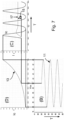
- the plot 52 shows the bias impedance Z BIAS produced by the bias circuit, while the plot 54 shows Z IN,OS , namely the impedance looking into the input of the output stage.
- Figure 2 illustrates that
- the bias circuit can control the gain compression through the variable capacitor 44 thereby to allow more or less RF swing at the control terminal (e.g. the base) of the transistor 40 as a function of RF drive level.
- variable reactance component e.g. the variable capacitor 44 (C 2 )
- the bias base voltage as function of input power can be effectively lowered. This can result in lower I bias vs power, resulting in less gain expansion and effectively a reduction of amplitude-to-amplitude (AM-to-AM) distortion making the amplifier more linear.
- the capacitive voltage divider can be made programmable through implementing the capacitor C 1 and/or the capacitor C 2 as a variable capacitor (e.g. variable reactance is implemented by the variable capacitor 44 (C 2 )). This can allow the amount of gain expansion correction to be variable/programmable. This can be a very useful property in an Error Vector Magnitude (EVM) trimming procedure during final test of a product incorporating the analog amplitude pre-distortion circuit 20.
- EVM Error Vector Magnitude
- Figure 3A shows:
- Figures 3A and 3B shows the AM-to-AM characteristics when varying the variable capacitor 44 (C 2 ), which may be considered to be an 'RF-ripple control capacitor'.
- the capacitance of the variable capacitor 44 (C 2 ) is zero, gain expansion in the AM-to-AM characteristic is observed.
- the AM-to-AM characteristic is nearly flat.
- the AM-to-AM characteristic exhibits gain compression.
- the circuit of Figure 1 may be modified to add a beta helper, so as to provide the bias circuit with a lower-ohmic output.
- a beta helper in accordance with these modifications:
- the beta helper can provide the bias circuit with a lower-ohmic output.
- the circuit may be less sensitive for the current gain (beta) of the transistor 30 and for the impedance of the DC-blocking capacitor at the RF input (modulation frequencies).
- the amplification of the RF signal provided by an amplification stage may be made more linear than can be achieved by prior circuits.
- the amount of gain expansion or gain compression may be reduced. This may be achieved by a bias circuit having a detector stage and a bias application stage, to be described below.
- Figure 4 shows an analog amplitude pre-distortion circuit 20 according to an embodiment of this disclosure. While the circuit of Figure 1 can provide unidirectional AM-to-AM linearity control, the embodiment of Figure 4 can provide bi-directional AM-to-AM linearity control. Unlike the circuit shown in Figure 1 , in the embodiments of Figures 4-9 , the function of detecting the amplitude of the RF signal received at the input 2 and the function of applying the bias to the amplifier stage input are performed separately (as opposed to both being performed by the transistor 40). Accordingly, in the embodiments of Figures 4-9 , a separate detector stage is provided, and the transistor 40 forms part of a bias application stage. It is this separation of the functions that may allow the bi-directional AM-to-AM linearity control to be achieved.
- the RF input 2, the amplifier stage (including, for example, the transistor 30) and the RF output 4 are configured in the same way as the corresponding RF input 2, the amplifier stage and RF output 4 in Figure 1 and accordingly the description of those features will therefore not be repeated here.
- the current source 32 is not coupled to the supply voltage V cc but is instead coupled to a bias voltage node 102, which applies a bias voltage V BIAS .
- the analog amplitude pre-distortion circuit 20 includes a bias application stage.
- the bias application stage includes a transistor 40 (Q 2 ), a resistor 42 (R 1 ) and a capacitor 46 (C 1 ).
- the transistor 40 (Q 2 ), a resistor 42 (R 1 ) and a capacitor 46 (C 1 ) are coupled together in much the same way as the corresponding transistor 40 (Q 2 ), a resistor 42 (R 1 ) and a capacitor 46 (C 1 ) shown in Figure 1 .
- the transistor 40 may, for instance be a bipolar junction transistor, although it is envisaged that it would be possible to use other kinds of transistor.
- a first current terminal e.g.
- a collector terminal) of the transistor 40 may be coupled to the amplifier stage input (e.g. to the control terminal (e.g. base terminal) of the transistor 30). Again, note that the first current terminal may thus also be coupled to the input 2.
- a second current terminal (e.g. an emitter terminal) of the transistor 40 is coupled to a reference voltage, e.g. to ground.
- the second current terminal of the transistor 40 is also coupled to a control terminal (e.g. base terminal) of the transistor 40 via a capacitor C 1 .
- the resistor 42 may be provided, and again the resistor 42 may be coupled between the control terminal (e.g. the base terminal) of the transistor 40 and the first current terminal (e.g. the collector terminal) of the transistor 40. Again, this resistor 42 may act to close the loop around the transistor 40 for DC and modulation frequencies.
- the resistor 42 in this embodiment is not coupled in parallel with a variable capacitor 44. Instead, while the resistor is coupled between the first current terminal and the control terminal of the transistor 40 the resistor 42, in this embodiment is also coupled across an node 76 and a node 78 of the detector stage 70 to be described below.
- the node 76 acts as an RF sense node of the detector stage, for detecting an amplitude of the RF signal received at the input 2
- the node 78 acts as an output of the detector stage 70, for outputting a correction signal to the bias application stage.
- the node 78 is coupled to the control terminal of the transistor 40, so that the correction signal may be applied to the control terminal.
- the correction signal is based on the detected amplitude of the RF signal.
- the correction signal takes the form of a current I cor .
- An output resistor 96 (R 4 ) may be coupled to the output node 78 for reducing the RF content in the current I cor to a desired range/level in accordance with design requirements.
- the RF sense input node 76 is coupled to the input 2 (e.g. via the DC-blocking capacitor 22), to receive the RF signal from the input.
- the detector stage 70 includes two variable reactance components: a first variable capacitor 82 (C 2 ) and a second variable capacitor 84 (C 3 ). A first terminal of the first variable capacitor 82 and a first terminal of the second variable capacitor 84 are coupled to the RF sense input node 76.
- the detector stage 70 also includes are first transistor 72 (Q 3 ) and a second transistor 74 (Q 4 ).
- the transistors 72, 74 may, for instance be bipolar junction transistors as shown in Figure 4 , although it is envisaged that it would be possible to use other kinds of transistor.
- a second terminal of the first variable capacitor 82 is coupled to a control terminal (e.g. base) of the first transistor 72, and a second terminal of the second variable capacitor 84 is coupled to a control terminal (e.g. a base terminal) of the second transistor 74.
- a first current terminal (e.g. an emitter terminal) of the first transistor 72 is coupled to a reference potential (e.g. ground) via a first capacitor 86 (C 4 ).
- a first current terminal (e.g. an emitter terminal) of the second transistor 74 is coupled to the reference potential (e.g. ground) via a second capacitor 88 (C 5 ).
- a second current terminal (e.g. a collector terminal) of the first transistor 72 is coupled to a first current source 104.
- the first current source 104 supplies a current I REF,apd .
- the first current source 104 may also be coupled to the bias voltage node 102.
- a second current terminal (e.g. a collector terminal) of the second transistor 74 is coupled to the output node 78 (e.g. via the output resistor 96).
- the second current terminal of the second transistor 74 is also coupled to a second current source 106.
- the second current source 106 supplies a current I REF,apd .
- the second current source 106 may also be coupled to the bias voltage node 102.
- the detector stage 70 may further include a first resistor 92 and a second resistor 94.
- the first resistor 92 may be coupled between the second current terminal of the first transistor 72 and the control terminal of the first transistor 72.
- the second resistor 94 may be coupled between the second current terminal of the first transistor 72 and the control terminal of the second transistor 74.
- the operation of the detector stage 70 in this embodiment which is aimed at improving the AM-to-AM transfer in both directions, may be as follows.
- FIG. 5 An illustration of the properties of the analog amplitude pre-distortion circuit 20 of Figure 4 are shown in Fig. 5 for an actual power amplifier circuit.
- Fig. 5 An illustration of the properties of the analog amplitude pre-distortion circuit 20 of Figure 4 are shown in Fig. 5 for an actual power amplifier circuit.
- Fig. 5 An illustration of the properties of the analog amplitude pre-distortion circuit 20 of Figure 4 are shown in Fig. 5 for an actual power amplifier circuit.
- Fig. 5 An illustration of the properties of the analog amplitude pre-distortion circuit 20 of Figure 4 are shown in Fig. 5 for an actual power amplifier circuit.
- the bias application stage is operable to apply a bias voltage at a first range of frequencies according to the amplitude of the RF signal at first impedances to the amplifier stage input, and to present second impedances at a second range of frequencies to the amplifier stage input.
- the embodiment of Figure 4 includes a bias application circuit, which bases the application of the bias voltage on a correction signal received from a separate detector stage.
- the bias application stage is operable to apply, according to the correction signal, a bias voltage at a first range of frequencies at first impedances to the amplifier stage input, and to present second impedances at a second range of frequencies to the amplifier stage input.
- the first impedances are lower than the second impedances and wherein the first range of frequencies are lower than the second range of frequencies.
- the first frequencies may, for instance, be DC and/or modulation frequencies.
- the second frequencies may, for instance, be the RF frequencies to be amplified by the amplification stage.
- Figure 6 shows an analog amplitude pre-distortion circuit 20 according to a further embodiment of this disclosure.
- the embodiment of Figure 6 is similar to the embodiment of Figure 4 and accordingly only the differences between Figure 6 and Figure 4 will be described below.
- the output of the detector stage 70 is coupled to an input of a correction signal modification block 110, to allow the correction signal modification block 110 to receive the correction signal (denoted I i in Figure 6 ).
- An output of the correction signal modification block 110 is coupled to the control terminal (e.g. base terminal) of the transistor 40, to allow the correction signal modification block 110 to pass a modified version of the correction signal (denoted I o in Figure 6 ) to the bias application stage.
- a resistor 112 may be coupled between the output of the correction signal modification block 110 and the control terminal (e.g. base terminal) of the transistor 40.
- the correction signal modification block 110 may also be coupled to the bias voltage node 102 and to the aforementioned reference potential (e.g. ground).
- the correction signal modification block 110 is operable to produce a modified correction signal based on the correction signal outputted by the detector stage 70. Consequently, in this embodiment, the bias application stage is operable to adjust the bias applied by the bias application stage to the amplifier stage input according to the modified correction signal produced by the correction signal modification block 110.
- the correction signal modification block 110 can apply any required modification function to the correction signal I i for producing the modified correction signal I o (e.g. in the current domain), which may in some embodiments be considered to be a "corrected" correction signal.
- modification function may comprise any of the following:
- the resistors 96 (R 4 ), 112 (R 5 ) may form a barrier for the RF signals (including higher harmonics), since the base-band transfer I i ⁇ I o of the arbitrary-function block and the operation of the transistor 40 might otherwise be adversely affected by the presence of RF-signals.
- FIG. 7 further illustrates a principle of operation of the circuit of Figure 1 and the embodiments of Figure 4 and 6 .
- Plot B shows the base-emitter voltage (V be ) 11 of a bipolar junction transistor as a function of time.
- Plot C shows the collector current (Ic) of the bipolar junction transistor as a function of time, and also the moving average 17 of Ic over time.
- Plot D shows the non-linear (substantially exponential, in this example) transfer function 13 (Ic as a function of V be ) of the bipolar junction transistor, for linking plot B to plot C.
- the transistor's non-linear transfer in plot D translates V be to a bias collector current Ic of 1 mA, as shown in plot C.
- V be of the second transistor 74 (Q 4 ) is shown in plot B of Figure 7 for t > 200 ps
- Ic of the second transistor 74 (Q 4 ) is shown in plot C of Figure 7
- the (unwanted) RF component in Ic may be (e.g. strongly) suppressed by the low-pass filter formed by the output capacitance of the second transistor 74 (Q 4 ), the resistor 96 (R 4 ) and (C 1 in parallel with C be2 ) (pi-network). After this low-pass filtering, only the moving-average value (bias component) of Ic remains (corresponding to moving average line 17). Initially, (e.g.
- the correction signal I cor will develop a bias voltage drop across R 1 .
- the first transistor 72 (Q 3 ) has a feedback resistor, namely the first resistor 92 (R 2 ), coupled between the collector and the base terminals of that transistor 72 (Q 3 ).
- the second transistor 74 (Q 4 ) does not have such a feedback resistor.
- the feedback resistor 92 (R 2 ) closes the loop around the first transistor 72 (Q 3 ) for DC and modulation frequencies. (However, for high frequencies (e.g. RF frequencies), the loop gain is relatively small due to the low-pass filter formed by the feedback resistor 92 (R 2 ) and the first capacitor 86 (C 4 ) in parallel with the base-emitter capacitance (C be3 ) of the first transistor 72 (Q 3 ).)
- the collector current (I C3 ) of the first transistor 72 (Q 3 ) is (almost) equal to L REF,apd .
- the collector current (I C3 ) of the first transistor 72 (Q 3 ) is (almost) equal to L REF,apd .
- the events as described above for the second transistor 74 (Q 4 ), will now occur for the first transistor 72 (Q 3 ): the RF-ripple voltage on the base of the first transistor 72 (Q 3 ) will result in an increase of its bias collector current I C3 . Since now I C3 becomes larger than I REF,apd , the current difference will flow through the feedback resistor 92 (R 2 ) and the second resistor 94 (R 3 ) and will discharge (C 4 in parallel with C be3 ) and (C 5 in parallel with C be4 ).
- the base-emitter voltage V be3 of the first transistor 72 (Q 3 ) (and also the base-emitter voltage V be4 of the second transistor 74 (Q 4 )) will gradually decrease, and finally I C3 will be (almost) equal again to I REF,apd .
- This process should be fast enough to follow the modulation of the RF-amplitude (the envelope of the carrier). Since V be4 also dropped, the collector current (I C4 ) of the second transistor 74 (Q 4 ) has now become smaller than I REF,apd .
- Figure 8 shows an analog amplitude pre-distortion circuit 20 according to another embodiment of this disclosure.
- multiple amplifier stages 6 1 , 6 2 ... 6 N may be linked together in series to form a linear chain of amplifier stages.
- a first amplifier stage 6 1 in the linear chain is coupled to the RF input 2 of the analog amplitude pre-distortion circuit 20.
- a final amplifier stage 6 N of the linear chain is coupled to the RF output 4 of the analog amplitude pre-distortion circuit 20.
- One or more intermediate amplifier stages (6 2 %) may each have an RF input which is coupled to an RF output of a preceding amplifier stage in the linear chain.
- the one or more intermediate amplifier stages (6 2 ...) may each have an RF output which is coupled to an RF input of a next amplifier stage in the linear chain.
- the RF input of the final amplifier stage 6 N is coupled to the RF output of the penultimate (6 (N-1) ) amplifier stage in the linear chain.
- the RF output of the first amplifier stage 6 1 is coupled to the RF input of the second amplifier stage 6 2 .
- Each amplifier stage in the linear chain may be an amplifier stage of the kind described above in relation to the preceding embodiments.
- the input of each amplifier stage in the linear chain may, for instance correspond to the RF input 2 of the amplifier stages shown in, for example, Figures 4 and 6 .
- the output of each amplifier stage in the linear chain may, for instance correspond to the RF output 4 of the amplifier stages shown in, for example, Figures 4 and 6 .
- each amplifier stage is provided with a respective detector stage and a respective bias application stage 9 of the kind described above.
- the detector stages are shown collectively in Figure 8 as block 8.
- the reactances (e.g. capacitors) of the various variable reactance components (e.g. variable capacitors) of the detector circuits in the block 8 may be controlled by control signals 14, thereby to tune the correction signals produced and outputted by those detector circuits to their respective bias application stages 9.
- a controller may be provided for providing the control signals 14, for programmably controlling the variable reactance components.
- the detector stage of each amplifier stage in the linear chain is coupled to the input of that amplifier stage (e.g. the output of a preceding amplifier stage in the linear chain) so as to sense the RF signal that is coupled into that amplifier stage.
- the bias application stages 9 are also coupled to their amplifier stages so as to adjust the bias voltage at each respective amplifier stage input according to the correction signal outputted by each respective detector stage.
- the various bias application stages may be provided within the block 8, it is also envisaged that the bias application stages may be considered to be included in the amplifier stages 6, or separately as shown in Figure 8 ( Figure 8 is schematic in this respect).
- the embodiment of Figure 8 can, on an amplifier block level, allow the freedom to choose where the RF input is sensed. Furthermore, the detector stages could be used to drive the bias input of any of the N amplifier stages in the linear chain. The embodiment of Figure 8 may allow each amplifier stage in the linear chain to receive an optimal scaled or post-processed bias signal.
- Figures 9A, 9B and 9C show various types of bias application stages that may be used according to further embodiments of this disclosure. According to embodiments of this disclosure, it is envisaged that bias application stages of the kinds shown in any of Figures 9A, 9B or 9C may be incorporated into any of the analog amplitude pre-distortion circuits described above.
- Each of the bias application stages described herein may also implement the function of an electronic, active gyrator.
- the gyrator function can operate to present (at the amplifier stage input) an active inductance, so as to allow the bias voltages applied by the bias application stage to have a desired inductive impedance, without needing to use an actual inductor component.
- Figure 9A will be recognised as being a bias application stage of the kind already described above in relation to, for example, Figures 4 and 6 and is shown again here in Figure 9A for comparison with the bias application stages shown in Figures 9B and 9C .
- the nodes 120, 130 in Figure 9A correspond to the node 78 and the node 76 in Figure 4 , respectively.
- the bias application stage shown in Figure 9B adds a further resistor 140 compared to the bias application stage of Figure 9A .
- the further resistor 140 is coupled between the node 130 (or the resistor 42) and the first current terminal (e.g. a collector terminal) of the transistor 40.
- the bias application stage of Figure 9B can operate as a low-noise gyrator compared to the bias application stage of Figure 9A .
- the bias application stage shown in Figure 9C adds a number of further components compared to the bias application stage of Figure 9B .
- the bias application stage of Figure 9C includes a further transistor 160.
- the further transistor 160 may be a bipolar junction transistor, although it is envisaged that it would be possible to use other kinds of transistor.
- a control terminal (e.g. a base terminal) of the further transistor is coupled to a voltage source 150, which supplies a voltage V CB,bias .
- the voltage source 150 is also coupled to the aforementioned reference potential (e.g. ground).
- the further transistor 160 is coupled between the first current terminal (e.g. a collector terminal) of the transistor 40 and the amplifier stage input (e.g. to the control terminal (e.g. base terminal) of the transistor 30).
- a first current terminal (e.g. a collector terminal) of the further transistor 160 may be coupled to the amplifier stage input and a second current terminal (e.g. an emitter terminal) of the further transistor 160 may be coupled to the first current terminal of the transistor 40.
- the control terminal (e.g. base) of transistor 30 is coupled to the terminal V OUT in Figure 9C .
- the bias application stage of Figure 9C also includes a further capacitor 144 and a further resistor 142 coupled together in series.
- the further capacitor 144 and further resistor 142 are coupled between the control terminal of the transistor 40 and the first current terminal of the further transistor 160.
- the resistor 140 is also coupled to the first current terminal of the further transistor 160, instead of to the first current terminal of the transistor 40 as shown in the embodiment of Figure 9B .
- the bias application stage of Figure 9C can operate as a low-noise gyrator compared to the bias application stage of Figure 9A and is further suited as a low memory effect gyrator bias circuit.
- an analog amplitude pre-distortion circuit 20 of the kind described herein may be provided within a power amplifier. In some embodiments, an analog amplitude pre-distortion circuit 20 of the kind described herein may be provided within a low-noise amplifier. Amplifiers of this kind may be used in, for example, Wireless Local Area Network (WLAN) front end modules (FEM). Amplifiers of this kind may also be used in, for example, millimeter wave analog beam forming (MMW ABF) applications. Amplifiers of this kind may further be used in, for example, driver and pre-driver applications for base station infrastructure.
- WLAN Wireless Local Area Network
- FEM front end modules
- MMW ABF millimeter wave analog beam forming
- an analog amplitude pre-distortion method includes receiving a Radio Frequency, RF, signal (e.g. at an input 2 of the kind described above) and using an amplifier stage (e.g. of the kind described above) to amplify the RF signal to produce an amplified RF signal.
- the method also includes applying bias voltages to an input of the amplifier stage.
- this may be achieved by (i) detecting an amplitude of the RF signal (ii) producing a correction signal based on the amplitude of the RF signal, (iii)applying, according to the correction signal, a bias voltage at a first range of frequencies at first impedances to the amplifier stage input, and (iv) presenting second impedances at a second range of frequencies to the amplifier stage input.
- the first impedances are lower than the second impedances and wherein the first range of frequencies are lower than the second range of frequencies.
- Steps (i) and (ii) may be performed by a detector stage of the kind described above.
- Steps (iii) and (iv) may be performed by a bias application stage of the kind described above.
- a beta helper maybe be added to the embodiments shown in either Figure 4 or Figure 6 , so as to provide the bias circuit with a lower-ohmic output.
- Figure 10 shows a modified version of Figure 4 in this respect, while Figure 11 shows a modified version of Figure 6 .
- the beta helper in the embodiments shown in Figures 10 and 11 can provide the bias circuit with a lower-ohmic output.
- the circuit may be less sensitive for the current gain (beta) of the transistor 30 and for the impedance of the DC-blocking capacitor at the RF input (modulation frequencies).
- the node coupled to the variable capacitor 82 (C 2 ) that is labelled “RF sense 1" and the node coupled to the variable capacitor 84 (C 3 ) that is labelled “RF sense 2" may be coupled to a number of different points in the circuit for sensing the RF signal.
- these nodes may be coupled to any of the following:
- the amount of AM-to-AM correction can not only be controlled with ripple capacitors 82 (C 2 ) and 84 (C 3 ), but also by changing the current I REF,apd produced by the current sources 104, 106.
- the current sources 104, 106 in Figures 10 and 11 are variable current sources, for modifying I REF,apd . This approach may be easier to implement (DC solution), compared to embodiments using programmable capacitors (RF). It is also envisaged that the variable current sources may be used in combination with the variable reactance components noted above.
- the circuit includes a Radio Frequency, RF, input for receiving an RF signal.
- the circuit also includes an amplifier stage comprising an amplifier stage input for receiving the RF signal from the RF input, wherein the amplifier stage is operable to amplify the RF signal to produce an amplified RF signal.
- the circuit further includes a bias circuit.
- the bias circuit includes a detector stage for detecting an amplitude of the RF signal, and for producing a correction signal based on the amplitude of the RF signal.
- the bias circuit also includes a bias application stage coupled to the amplifier stage input.
- the bias application stage is operable to apply, according to the correction signal, a bias voltage at a first range of frequencies at first impedances to the amplifier stage input.
- the bias application circuit is also operable to present second impedances at a second range of frequencies to the amplifier stage input.
- the first impedances are lower than the second impedances.
- the first range of frequencies are lower than the second range of frequencies.
Landscapes
- Engineering & Computer Science (AREA)
- Power Engineering (AREA)
- Physics & Mathematics (AREA)
- Nonlinear Science (AREA)
- Microelectronics & Electronic Packaging (AREA)
- Amplifiers (AREA)
Priority Applications (2)
| Application Number | Priority Date | Filing Date | Title |
|---|---|---|---|
| EP22306051.8A EP4307563A1 (fr) | 2022-07-13 | 2022-07-13 | Circuit et procédé de prédistorsion d'amplitude analogique |
| US18/348,415 US20240022216A1 (en) | 2022-07-13 | 2023-07-07 | Analog amplitude pre-distortion circuit and method |
Applications Claiming Priority (1)
| Application Number | Priority Date | Filing Date | Title |
|---|---|---|---|
| EP22306051.8A EP4307563A1 (fr) | 2022-07-13 | 2022-07-13 | Circuit et procédé de prédistorsion d'amplitude analogique |
Publications (1)
| Publication Number | Publication Date |
|---|---|
| EP4307563A1 true EP4307563A1 (fr) | 2024-01-17 |
Family
ID=82846356
Family Applications (1)
| Application Number | Title | Priority Date | Filing Date |
|---|---|---|---|
| EP22306051.8A Pending EP4307563A1 (fr) | 2022-07-13 | 2022-07-13 | Circuit et procédé de prédistorsion d'amplitude analogique |
Country Status (2)
| Country | Link |
|---|---|
| US (1) | US20240022216A1 (fr) |
| EP (1) | EP4307563A1 (fr) |
Citations (4)
| Publication number | Priority date | Publication date | Assignee | Title |
|---|---|---|---|---|
| JP2003273660A (ja) * | 2002-03-15 | 2003-09-26 | Mitsubishi Electric Corp | 高周波増幅器 |
| US20080036534A1 (en) * | 2006-08-14 | 2008-02-14 | Ren-Chieh Liu | Power amplifier circuit having a bias signal inputted into input terminal and method thereof |
| US20180006611A1 (en) * | 2016-06-30 | 2018-01-04 | Nxp B.V. | Doherty amplifier circuits |
| US20180234057A1 (en) * | 2017-02-15 | 2018-08-16 | Richwave Technology Corp. | Predistorter for compensating linearity of an amplifier |
-
2022
- 2022-07-13 EP EP22306051.8A patent/EP4307563A1/fr active Pending
-
2023
- 2023-07-07 US US18/348,415 patent/US20240022216A1/en active Pending
Patent Citations (4)
| Publication number | Priority date | Publication date | Assignee | Title |
|---|---|---|---|---|
| JP2003273660A (ja) * | 2002-03-15 | 2003-09-26 | Mitsubishi Electric Corp | 高周波増幅器 |
| US20080036534A1 (en) * | 2006-08-14 | 2008-02-14 | Ren-Chieh Liu | Power amplifier circuit having a bias signal inputted into input terminal and method thereof |
| US20180006611A1 (en) * | 2016-06-30 | 2018-01-04 | Nxp B.V. | Doherty amplifier circuits |
| US20180234057A1 (en) * | 2017-02-15 | 2018-08-16 | Richwave Technology Corp. | Predistorter for compensating linearity of an amplifier |
Also Published As
| Publication number | Publication date |
|---|---|
| US20240022216A1 (en) | 2024-01-18 |
Similar Documents
| Publication | Publication Date | Title |
|---|---|---|
| US7863976B1 (en) | Adjustable segmented power amplifier | |
| US7917117B2 (en) | Auto-tuning amplifier | |
| CN110677132B (zh) | 一种射频线性功率放大器电路 | |
| US7675364B2 (en) | Circuit and method of establishing DC bias levels in an RF power amplifier | |
| US9099964B2 (en) | High-frequency signal processing device | |
| CN109639244A (zh) | 用于偏置rf电路的系统和方法 | |
| CN103534940A (zh) | 正反馈共栅极低噪声放大器 | |
| WO2022205975A1 (fr) | Circuit de polarisation et amplificateur de puissance radiofréquence | |
| KR20020025701A (ko) | 증폭회로 | |
| US7113045B2 (en) | Power amplifier input structure having a differential output | |
| CN100461622C (zh) | 用于时分双工模式的低时延温度补偿偏置电路 | |
| EP2110947A1 (fr) | Amplificateur RF à gain variable | |
| JP7258612B2 (ja) | 高周波回路 | |
| US6972627B2 (en) | High frequency power amplifier module | |
| US7332963B2 (en) | Low noise amplifier | |
| CN110880919A (zh) | 改进的放大器和用于放大输入信号的方法 | |
| CN108134585B (zh) | 射频功率放大电路及其超带宽输出匹配电路 | |
| Vintola et al. | Variable-gain power amplifier for mobile WCDMA applications | |
| EP4307563A1 (fr) | Circuit et procédé de prédistorsion d'amplitude analogique | |
| US7212070B2 (en) | Circuit and method of reducing noise in an RF power amplifier | |
| US20220278651A1 (en) | Barely doherty dual envelope tracking (bd2e) circuit | |
| US20240022218A1 (en) | Analog amplitude pre-distortion circuit and method | |
| CN112398448B (zh) | 射频差分放大电路和射频模组 | |
| US9614498B2 (en) | Active balun circuit and transformer | |
| US5606294A (en) | Automatic gain control circuit and method |
Legal Events
| Date | Code | Title | Description |
|---|---|---|---|
| PUAI | Public reference made under article 153(3) epc to a published international application that has entered the european phase |
Free format text: ORIGINAL CODE: 0009012 |
|
| STAA | Information on the status of an ep patent application or granted ep patent |
Free format text: STATUS: THE APPLICATION HAS BEEN PUBLISHED |
|
| AK | Designated contracting states |
Kind code of ref document: A1 Designated state(s): AL AT BE BG CH CY CZ DE DK EE ES FI FR GB GR HR HU IE IS IT LI LT LU LV MC MK MT NL NO PL PT RO RS SE SI SK SM TR |