EP4306676A1 - Semiconductor device - Google Patents
Semiconductor device Download PDFInfo
- Publication number
- EP4306676A1 EP4306676A1 EP22767184.9A EP22767184A EP4306676A1 EP 4306676 A1 EP4306676 A1 EP 4306676A1 EP 22767184 A EP22767184 A EP 22767184A EP 4306676 A1 EP4306676 A1 EP 4306676A1
- Authority
- EP
- European Patent Office
- Prior art keywords
- film
- substrate
- nozzle
- mist
- raw material
- Prior art date
- Legal status (The legal status is an assumption and is not a legal conclusion. Google has not performed a legal analysis and makes no representation as to the accuracy of the status listed.)
- Pending
Links
Images


Classifications
-
- H—ELECTRICITY
- H10—SEMICONDUCTOR DEVICES; ELECTRIC SOLID-STATE DEVICES NOT OTHERWISE PROVIDED FOR
- H10P—GENERIC PROCESSES OR APPARATUS FOR THE MANUFACTURE OR TREATMENT OF DEVICES COVERED BY CLASS H10
- H10P14/00—Formation of materials, e.g. in the shape of layers or pillars
- H10P14/20—Formation of materials, e.g. in the shape of layers or pillars of semiconductor materials
- H10P14/34—Deposited materials, e.g. layers
- H10P14/3402—Deposited materials, e.g. layers characterised by the chemical composition
- H10P14/3434—Deposited materials, e.g. layers characterised by the chemical composition being oxide semiconductor materials
-
- C—CHEMISTRY; METALLURGY
- C23—COATING METALLIC MATERIAL; COATING MATERIAL WITH METALLIC MATERIAL; CHEMICAL SURFACE TREATMENT; DIFFUSION TREATMENT OF METALLIC MATERIAL; COATING BY VACUUM EVAPORATION, BY SPUTTERING, BY ION IMPLANTATION OR BY CHEMICAL VAPOUR DEPOSITION, IN GENERAL; INHIBITING CORROSION OF METALLIC MATERIAL OR INCRUSTATION IN GENERAL
- C23C—COATING METALLIC MATERIAL; COATING MATERIAL WITH METALLIC MATERIAL; SURFACE TREATMENT OF METALLIC MATERIAL BY DIFFUSION INTO THE SURFACE, BY CHEMICAL CONVERSION OR SUBSTITUTION; COATING BY VACUUM EVAPORATION, BY SPUTTERING, BY ION IMPLANTATION OR BY CHEMICAL VAPOUR DEPOSITION, IN GENERAL
- C23C16/00—Chemical coating by decomposition of gaseous compounds, without leaving reaction products of surface material in the coating, i.e. chemical vapour deposition [CVD] processes
- C23C16/22—Chemical coating by decomposition of gaseous compounds, without leaving reaction products of surface material in the coating, i.e. chemical vapour deposition [CVD] processes characterised by the deposition of inorganic material, other than metallic material
- C23C16/30—Deposition of compounds, mixtures or solid solutions, e.g. borides, carbides, nitrides
- C23C16/40—Oxides
-
- C—CHEMISTRY; METALLURGY
- C23—COATING METALLIC MATERIAL; COATING MATERIAL WITH METALLIC MATERIAL; CHEMICAL SURFACE TREATMENT; DIFFUSION TREATMENT OF METALLIC MATERIAL; COATING BY VACUUM EVAPORATION, BY SPUTTERING, BY ION IMPLANTATION OR BY CHEMICAL VAPOUR DEPOSITION, IN GENERAL; INHIBITING CORROSION OF METALLIC MATERIAL OR INCRUSTATION IN GENERAL
- C23C—COATING METALLIC MATERIAL; COATING MATERIAL WITH METALLIC MATERIAL; SURFACE TREATMENT OF METALLIC MATERIAL BY DIFFUSION INTO THE SURFACE, BY CHEMICAL CONVERSION OR SUBSTITUTION; COATING BY VACUUM EVAPORATION, BY SPUTTERING, BY ION IMPLANTATION OR BY CHEMICAL VAPOUR DEPOSITION, IN GENERAL
- C23C16/00—Chemical coating by decomposition of gaseous compounds, without leaving reaction products of surface material in the coating, i.e. chemical vapour deposition [CVD] processes
- C23C16/44—Chemical coating by decomposition of gaseous compounds, without leaving reaction products of surface material in the coating, i.e. chemical vapour deposition [CVD] processes characterised by the method of coating
- C23C16/448—Chemical coating by decomposition of gaseous compounds, without leaving reaction products of surface material in the coating, i.e. chemical vapour deposition [CVD] processes characterised by the method of coating characterised by the method used for generating reactive gas streams, e.g. by evaporation or sublimation of precursor materials
- C23C16/4485—Chemical coating by decomposition of gaseous compounds, without leaving reaction products of surface material in the coating, i.e. chemical vapour deposition [CVD] processes characterised by the method of coating characterised by the method used for generating reactive gas streams, e.g. by evaporation or sublimation of precursor materials by evaporation without using carrier gas in contact with the source material
-
- C—CHEMISTRY; METALLURGY
- C23—COATING METALLIC MATERIAL; COATING MATERIAL WITH METALLIC MATERIAL; CHEMICAL SURFACE TREATMENT; DIFFUSION TREATMENT OF METALLIC MATERIAL; COATING BY VACUUM EVAPORATION, BY SPUTTERING, BY ION IMPLANTATION OR BY CHEMICAL VAPOUR DEPOSITION, IN GENERAL; INHIBITING CORROSION OF METALLIC MATERIAL OR INCRUSTATION IN GENERAL
- C23C—COATING METALLIC MATERIAL; COATING MATERIAL WITH METALLIC MATERIAL; SURFACE TREATMENT OF METALLIC MATERIAL BY DIFFUSION INTO THE SURFACE, BY CHEMICAL CONVERSION OR SUBSTITUTION; COATING BY VACUUM EVAPORATION, BY SPUTTERING, BY ION IMPLANTATION OR BY CHEMICAL VAPOUR DEPOSITION, IN GENERAL
- C23C16/00—Chemical coating by decomposition of gaseous compounds, without leaving reaction products of surface material in the coating, i.e. chemical vapour deposition [CVD] processes
- C23C16/44—Chemical coating by decomposition of gaseous compounds, without leaving reaction products of surface material in the coating, i.e. chemical vapour deposition [CVD] processes characterised by the method of coating
- C23C16/448—Chemical coating by decomposition of gaseous compounds, without leaving reaction products of surface material in the coating, i.e. chemical vapour deposition [CVD] processes characterised by the method of coating characterised by the method used for generating reactive gas streams, e.g. by evaporation or sublimation of precursor materials
- C23C16/4486—Chemical coating by decomposition of gaseous compounds, without leaving reaction products of surface material in the coating, i.e. chemical vapour deposition [CVD] processes characterised by the method of coating characterised by the method used for generating reactive gas streams, e.g. by evaporation or sublimation of precursor materials by producing an aerosol and subsequent evaporation of the droplets or particles
-
- C—CHEMISTRY; METALLURGY
- C23—COATING METALLIC MATERIAL; COATING MATERIAL WITH METALLIC MATERIAL; CHEMICAL SURFACE TREATMENT; DIFFUSION TREATMENT OF METALLIC MATERIAL; COATING BY VACUUM EVAPORATION, BY SPUTTERING, BY ION IMPLANTATION OR BY CHEMICAL VAPOUR DEPOSITION, IN GENERAL; INHIBITING CORROSION OF METALLIC MATERIAL OR INCRUSTATION IN GENERAL
- C23C—COATING METALLIC MATERIAL; COATING MATERIAL WITH METALLIC MATERIAL; SURFACE TREATMENT OF METALLIC MATERIAL BY DIFFUSION INTO THE SURFACE, BY CHEMICAL CONVERSION OR SUBSTITUTION; COATING BY VACUUM EVAPORATION, BY SPUTTERING, BY ION IMPLANTATION OR BY CHEMICAL VAPOUR DEPOSITION, IN GENERAL
- C23C16/00—Chemical coating by decomposition of gaseous compounds, without leaving reaction products of surface material in the coating, i.e. chemical vapour deposition [CVD] processes
- C23C16/44—Chemical coating by decomposition of gaseous compounds, without leaving reaction products of surface material in the coating, i.e. chemical vapour deposition [CVD] processes characterised by the method of coating
- C23C16/455—Chemical coating by decomposition of gaseous compounds, without leaving reaction products of surface material in the coating, i.e. chemical vapour deposition [CVD] processes characterised by the method of coating characterised by the method used for introducing gases into reaction chamber or for modifying gas flows in reaction chamber
- C23C16/45563—Gas nozzles
-
- C—CHEMISTRY; METALLURGY
- C23—COATING METALLIC MATERIAL; COATING MATERIAL WITH METALLIC MATERIAL; CHEMICAL SURFACE TREATMENT; DIFFUSION TREATMENT OF METALLIC MATERIAL; COATING BY VACUUM EVAPORATION, BY SPUTTERING, BY ION IMPLANTATION OR BY CHEMICAL VAPOUR DEPOSITION, IN GENERAL; INHIBITING CORROSION OF METALLIC MATERIAL OR INCRUSTATION IN GENERAL
- C23C—COATING METALLIC MATERIAL; COATING MATERIAL WITH METALLIC MATERIAL; SURFACE TREATMENT OF METALLIC MATERIAL BY DIFFUSION INTO THE SURFACE, BY CHEMICAL CONVERSION OR SUBSTITUTION; COATING BY VACUUM EVAPORATION, BY SPUTTERING, BY ION IMPLANTATION OR BY CHEMICAL VAPOUR DEPOSITION, IN GENERAL
- C23C16/00—Chemical coating by decomposition of gaseous compounds, without leaving reaction products of surface material in the coating, i.e. chemical vapour deposition [CVD] processes
- C23C16/44—Chemical coating by decomposition of gaseous compounds, without leaving reaction products of surface material in the coating, i.e. chemical vapour deposition [CVD] processes characterised by the method of coating
- C23C16/46—Chemical coating by decomposition of gaseous compounds, without leaving reaction products of surface material in the coating, i.e. chemical vapour deposition [CVD] processes characterised by the method of coating characterised by the method used for heating the substrate
-
- C—CHEMISTRY; METALLURGY
- C23—COATING METALLIC MATERIAL; COATING MATERIAL WITH METALLIC MATERIAL; CHEMICAL SURFACE TREATMENT; DIFFUSION TREATMENT OF METALLIC MATERIAL; COATING BY VACUUM EVAPORATION, BY SPUTTERING, BY ION IMPLANTATION OR BY CHEMICAL VAPOUR DEPOSITION, IN GENERAL; INHIBITING CORROSION OF METALLIC MATERIAL OR INCRUSTATION IN GENERAL
- C23C—COATING METALLIC MATERIAL; COATING MATERIAL WITH METALLIC MATERIAL; SURFACE TREATMENT OF METALLIC MATERIAL BY DIFFUSION INTO THE SURFACE, BY CHEMICAL CONVERSION OR SUBSTITUTION; COATING BY VACUUM EVAPORATION, BY SPUTTERING, BY ION IMPLANTATION OR BY CHEMICAL VAPOUR DEPOSITION, IN GENERAL
- C23C16/00—Chemical coating by decomposition of gaseous compounds, without leaving reaction products of surface material in the coating, i.e. chemical vapour deposition [CVD] processes
- C23C16/44—Chemical coating by decomposition of gaseous compounds, without leaving reaction products of surface material in the coating, i.e. chemical vapour deposition [CVD] processes characterised by the method of coating
- C23C16/52—Controlling or regulating the coating process
-
- H—ELECTRICITY
- H10—SEMICONDUCTOR DEVICES; ELECTRIC SOLID-STATE DEVICES NOT OTHERWISE PROVIDED FOR
- H10D—INORGANIC ELECTRIC SEMICONDUCTOR DEVICES
- H10D62/00—Semiconductor bodies, or regions thereof, of devices having potential barriers
- H10D62/40—Crystalline structures
-
- H—ELECTRICITY
- H10—SEMICONDUCTOR DEVICES; ELECTRIC SOLID-STATE DEVICES NOT OTHERWISE PROVIDED FOR
- H10D—INORGANIC ELECTRIC SEMICONDUCTOR DEVICES
- H10D62/00—Semiconductor bodies, or regions thereof, of devices having potential barriers
- H10D62/80—Semiconductor bodies, or regions thereof, of devices having potential barriers characterised by the materials
-
- H—ELECTRICITY
- H10—SEMICONDUCTOR DEVICES; ELECTRIC SOLID-STATE DEVICES NOT OTHERWISE PROVIDED FOR
- H10P—GENERIC PROCESSES OR APPARATUS FOR THE MANUFACTURE OR TREATMENT OF DEVICES COVERED BY CLASS H10
- H10P14/00—Formation of materials, e.g. in the shape of layers or pillars
- H10P14/20—Formation of materials, e.g. in the shape of layers or pillars of semiconductor materials
- H10P14/24—Formation of materials, e.g. in the shape of layers or pillars of semiconductor materials using chemical vapour deposition [CVD]
-
- H—ELECTRICITY
- H10—SEMICONDUCTOR DEVICES; ELECTRIC SOLID-STATE DEVICES NOT OTHERWISE PROVIDED FOR
- H10P—GENERIC PROCESSES OR APPARATUS FOR THE MANUFACTURE OR TREATMENT OF DEVICES COVERED BY CLASS H10
- H10P14/00—Formation of materials, e.g. in the shape of layers or pillars
- H10P14/20—Formation of materials, e.g. in the shape of layers or pillars of semiconductor materials
- H10P14/26—Formation of materials, e.g. in the shape of layers or pillars of semiconductor materials using liquid deposition
- H10P14/265—Formation of materials, e.g. in the shape of layers or pillars of semiconductor materials using liquid deposition using solutions
-
- H—ELECTRICITY
- H10—SEMICONDUCTOR DEVICES; ELECTRIC SOLID-STATE DEVICES NOT OTHERWISE PROVIDED FOR
- H10P—GENERIC PROCESSES OR APPARATUS FOR THE MANUFACTURE OR TREATMENT OF DEVICES COVERED BY CLASS H10
- H10P14/00—Formation of materials, e.g. in the shape of layers or pillars
- H10P14/20—Formation of materials, e.g. in the shape of layers or pillars of semiconductor materials
- H10P14/29—Formation of materials, e.g. in the shape of layers or pillars of semiconductor materials characterised by the substrates
- H10P14/2901—Materials
- H10P14/2921—Materials being crystalline insulating materials
-
- H—ELECTRICITY
- H10—SEMICONDUCTOR DEVICES; ELECTRIC SOLID-STATE DEVICES NOT OTHERWISE PROVIDED FOR
- H10P—GENERIC PROCESSES OR APPARATUS FOR THE MANUFACTURE OR TREATMENT OF DEVICES COVERED BY CLASS H10
- H10P14/00—Formation of materials, e.g. in the shape of layers or pillars
- H10P14/20—Formation of materials, e.g. in the shape of layers or pillars of semiconductor materials
- H10P14/32—Formation of materials, e.g. in the shape of layers or pillars of semiconductor materials characterised by intermediate layers between substrates and deposited layers
- H10P14/3202—Materials thereof
- H10P14/3234—Materials thereof being oxide semiconducting materials
-
- H—ELECTRICITY
- H10—SEMICONDUCTOR DEVICES; ELECTRIC SOLID-STATE DEVICES NOT OTHERWISE PROVIDED FOR
- H10P—GENERIC PROCESSES OR APPARATUS FOR THE MANUFACTURE OR TREATMENT OF DEVICES COVERED BY CLASS H10
- H10P14/00—Formation of materials, e.g. in the shape of layers or pillars
- H10P14/20—Formation of materials, e.g. in the shape of layers or pillars of semiconductor materials
- H10P14/32—Formation of materials, e.g. in the shape of layers or pillars of semiconductor materials characterised by intermediate layers between substrates and deposited layers
- H10P14/3202—Materials thereof
- H10P14/3238—Materials thereof being insulating materials
-
- H—ELECTRICITY
- H10—SEMICONDUCTOR DEVICES; ELECTRIC SOLID-STATE DEVICES NOT OTHERWISE PROVIDED FOR
- H10P—GENERIC PROCESSES OR APPARATUS FOR THE MANUFACTURE OR TREATMENT OF DEVICES COVERED BY CLASS H10
- H10P14/00—Formation of materials, e.g. in the shape of layers or pillars
- H10P14/20—Formation of materials, e.g. in the shape of layers or pillars of semiconductor materials
- H10P14/34—Deposited materials, e.g. layers
- H10P14/3438—Doping during depositing
- H10P14/3441—Conductivity type
- H10P14/3442—N-type
-
- H—ELECTRICITY
- H10—SEMICONDUCTOR DEVICES; ELECTRIC SOLID-STATE DEVICES NOT OTHERWISE PROVIDED FOR
- H10P—GENERIC PROCESSES OR APPARATUS FOR THE MANUFACTURE OR TREATMENT OF DEVICES COVERED BY CLASS H10
- H10P14/00—Formation of materials, e.g. in the shape of layers or pillars
- H10P14/20—Formation of materials, e.g. in the shape of layers or pillars of semiconductor materials
- H10P14/34—Deposited materials, e.g. layers
- H10P14/3438—Doping during depositing
- H10P14/3441—Conductivity type
- H10P14/3444—P-type
-
- H—ELECTRICITY
- H10—SEMICONDUCTOR DEVICES; ELECTRIC SOLID-STATE DEVICES NOT OTHERWISE PROVIDED FOR
- H10P—GENERIC PROCESSES OR APPARATUS FOR THE MANUFACTURE OR TREATMENT OF DEVICES COVERED BY CLASS H10
- H10P14/00—Formation of materials, e.g. in the shape of layers or pillars
- H10P14/20—Formation of materials, e.g. in the shape of layers or pillars of semiconductor materials
- H10P14/34—Deposited materials, e.g. layers
- H10P14/3438—Doping during depositing
- H10P14/3441—Conductivity type
- H10P14/3446—Transition metal elements; Rare earth elements
-
- H—ELECTRICITY
- H10—SEMICONDUCTOR DEVICES; ELECTRIC SOLID-STATE DEVICES NOT OTHERWISE PROVIDED FOR
- H10P—GENERIC PROCESSES OR APPARATUS FOR THE MANUFACTURE OR TREATMENT OF DEVICES COVERED BY CLASS H10
- H10P14/00—Formation of materials, e.g. in the shape of layers or pillars
- H10P14/20—Formation of materials, e.g. in the shape of layers or pillars of semiconductor materials
- H10P14/34—Deposited materials, e.g. layers
- H10P14/3451—Structure
- H10P14/3452—Microstructure
-
- H—ELECTRICITY
- H10—SEMICONDUCTOR DEVICES; ELECTRIC SOLID-STATE DEVICES NOT OTHERWISE PROVIDED FOR
- H10P—GENERIC PROCESSES OR APPARATUS FOR THE MANUFACTURE OR TREATMENT OF DEVICES COVERED BY CLASS H10
- H10P14/00—Formation of materials, e.g. in the shape of layers or pillars
- H10P14/60—Formation of materials, e.g. in the shape of layers or pillars of insulating materials
- H10P14/63—Formation of materials, e.g. in the shape of layers or pillars of insulating materials characterised by the formation processes
- H10P14/6326—Deposition processes
- H10P14/6328—Deposition from the gas or vapour phase
- H10P14/6334—Deposition from the gas or vapour phase using decomposition or reaction of gaseous or vapour phase compounds, i.e. chemical vapour deposition
-
- H—ELECTRICITY
- H10—SEMICONDUCTOR DEVICES; ELECTRIC SOLID-STATE DEVICES NOT OTHERWISE PROVIDED FOR
- H10P—GENERIC PROCESSES OR APPARATUS FOR THE MANUFACTURE OR TREATMENT OF DEVICES COVERED BY CLASS H10
- H10P14/00—Formation of materials, e.g. in the shape of layers or pillars
- H10P14/60—Formation of materials, e.g. in the shape of layers or pillars of insulating materials
- H10P14/69—Inorganic materials
- H10P14/692—Inorganic materials composed of oxides, glassy oxides or oxide-based glasses
- H10P14/6938—Inorganic materials composed of oxides, glassy oxides or oxide-based glasses the material containing at least one metal element, e.g. metal oxides, metal oxynitrides or metal oxycarbides
- H10P14/6939—Inorganic materials composed of oxides, glassy oxides or oxide-based glasses the material containing at least one metal element, e.g. metal oxides, metal oxynitrides or metal oxycarbides characterised by the metal
Definitions
- the present invention relates to a film-forming method for performing a film-formation on a substrate using a mist-like raw material solution.
- a high-vacuum film-formation apparatus that can achieve non-equilibrium state, such as pulsed laser deposition (PLD), molecular beam epitaxy (MBE), and sputtering, have been developed, enabling to fabricate an oxide semiconductor that was previously impossible to fabricate using a conventional method such as a melt method.
- Mist chemical vapor deposition (hereinafter referred to as a mist CVD method) using the atomized mist-like raw material solution to grow crystal on a substrate, has also been developed, enabling to fabricate a gallium oxide ( ⁇ -Ga 2 O 3 ) having a corundum structure.
- ⁇ -Ga 2 O 3 As a semiconductor with a large band gap, ⁇ -Ga 2 O 3 is expected to be applied to next-generation switching device that can achieve high-voltage, low loss, and high heat resistance.
- Patent Document 1 describes a tubular furnace type mist CVD apparatus.
- Patent Document 2 describes a fine channel type mist CVD apparatus.
- Patent Document 3 describes a linear source type mist CVD apparatus.
- Patent Document 4 describes a mist CVD apparatus of a tubular furnace, which differs from the mist CVD apparatus described in Patent Document 1 in that a carrier gas is introduced into a mist generator.
- Patent Document 5 describes a mist CVD apparatus in which a substrate is placed above a mist generator and a susceptor is a rotating stage mounted on a hot plate.
- the mist CVD method can perform a film-formation at relatively low temperatures, and it is also possible to fabricate a crystal structure of a metastable phase such as the corundum structure of ⁇ -Ga 2 O 3 .
- the present inventors found that when the film-formation is performed using the mist CVD method, pits are formed on a film surface, resulting in the film surface having poor surface smoothness.
- a film including many pits causes the pits to be killer defect, resulting in dielectric breakdown of a semiconductor apparatus.
- removal of the pits by polishing is problematic due to increasing the number of processes in creating the semiconductor apparatus.
- the present invention has been made to solve the above-described problems.
- An object of the present invention to provide: a film having suppressed pits and good surface smoothness; and a film-forming method for performing a film-formation such a film.
- the present invention has been made to achieve the above object.
- the present invention provides an oxide semiconductor film including gallium as main component, the oxide semiconductor film having a corundum structure, wherein pits on the surface of the oxide semiconductor film are 10000 pits/cm 2 or less.
- Such oxide semiconductor film is simply and inexpensively obtained, and moreover has excellent surface smoothness, allowing to use suitable for a semiconductor apparatus.
- the pits on the surface of the oxide semiconductor film can be 100 pits/cm 2 or less.
- the oxide semiconductor film can have an area of 10 cm 2 or more.
- the pits on the surface of the oxide semiconductor film have an opening diameter of 10 nm to 10 ⁇ m and the pits have a depth of 10 nm to 10 pm.
- the semiconductor apparatus can include the above oxide semiconductor film.
- the present invention also provides a film-forming method for heat-treating a raw material solution atomized into a mist and performing a film-formation, the method includes the following steps:
- the pits on the surface are suppressed, and thus the film having good smoothness can be formed.
- the raw material solution can contain gallium.
- the raw material solution can contain halogen.
- the mist can be supplied to the substrate from the nozzle provided vertically above the substrate.
- the substrate can be moved under the nozzle.
- the opening surface of the nozzle can be rectangular.
- the area of the substrate can be 10 cm 2 or more.
- the oxide semiconductor film according to the present invention can reduce the pits, have the excellent smoothness on the surface, and can be used suitable for the semiconductor apparatus.
- the film-forming method according to the present invention allows to form the film having fewer pits on the surface and good smoothness by way of simple method in the mist CVD method.
- an oxide semiconductor film including gallium as main component, the oxide semiconductor film having a corundum structure, wherein pits on the surface of the oxide semiconductor film are 10000 pits/cm 2 or less, can be simply and inexpensively obtained, has the excellent surface smoothness, and can be used suitably for a semiconductor apparatus. This finding has led to the completion of the present invention.
- a film-forming method for heat-treating a raw material solution atomized into a mist and performing a film-formation including the following steps: atomizing the raw material solution or making the raw material solution into droplets to generate a mist; conveying the mist to a film-forming part by a carrier gas; and supplying the mist from a nozzle to a substrate, heat-treating the mist on the substrate, and performing the film-formation in the film-forming part, wherein with the area of an opening surface of the nozzle being S [cm 2 ], the longest distance among distances between points in the opening surface and the surface of the substrate being H [cm], and the flow rate of the carrier gas supplied from the nozzle being Q [L/min], SH/Q ⁇ 0.015 results, enables to form a film with fewer pits and good smoothness. This finding has led to the completion of the present invention.
- An oxide semiconductor film according to the present invention includes gallium as main component, and has a corundum structure, wherein pits on the surface of the oxide semiconductor film are 10000 pits/cm 2 or less. While an oxide semiconductor film is typically composed of metal and oxygen, in the oxide semiconductor film according to the present invention, the metal contains gallium as main component. Herein, termed a main component means that 50 to 100% of the metal component is gallium. Termed a "gallium-based" means that the metal contains gallium as a metal component. Examples of metal components other than gallium may include one or more metals selected from iron, indium, aluminum, vanadium, titanium, chromium, rhodium, iridium, nickel, and cobalt.
- the pits are preferably less than 10000 pits/cm 2 , more preferably 100 pits/cm 2 or less, and even more preferably less than 100 pits/cm 2 . Although a lower limit of the pits is not particularly limited, it may be 0.01 pits/cm 2 or more.
- Dopants can be included in the oxide semiconductor film depending on the application.
- Examples of dopants include, but not particularly limited to, n- type dopants such as tin, germanium, silicon, titanium, zirconium, vanadium, or niobium, or p-type dopants such as copper, silver, tin, iridium, or rhodium.
- the concentration of dopants may be, for example, about 1.0 ⁇ 10 16 to 1.0 ⁇ 10 22 /cm 3 , and may be as low as about 1.0 ⁇ 10 17 /cm 3 or less, or as high as about 1.0 ⁇ 10 20 /cm 3 or more.
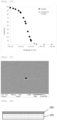
- a pit in the present invention represents a recess formed on the film surface as shown in FIG. 15 , and can be observed by an optical microscope, SEM, TEM, etc.
- the opening diameter of the pit is about 10 nm to 10 ⁇ m, and the depth of the pit is 10 nm to 10 pm.
- the conditions described hereafter can reduce the velocity component of the mist in the direction orthogonal to the substrate and the weight (moisture content) of the mist at the point of arrival at the substrate to reduce, thereby suppressing a pit-formation.
- the film thickness is not particularly limited. For example, it may be 0.05 to 100 ⁇ m, preferably 0.1 to 50 ⁇ m, and more preferably 0.5 to 20 pm.
- the oxide semiconductor film 180 according to the present invention is formed on the substrate 181 as shown in FIG. 16 .
- the other layer may be interposed between the substrate 181 and the oxide semiconductor film 180.
- the other layer refers to a layer that differs in composition from the substrate 181 and the topmost oxide semiconductor film 180. It can be, for example, a crystalline oxide film, an insulating film, or a metal film.
- the oxide semiconductor film preferably has an area of 10 cm 2 or more, and if circular, a diameter of 2 inches (50 mm) or more is preferable.
- the upper limit of the area is not particularly limited, it is preferably 750 cm 2 or less, and if circular, the diameter of 12 inches (300 mm) or less is preferable.
- the oxide semiconductor film according to the present invention can be used in a semiconductor apparatus by performing an appropriate structural design.
- the oxide semiconductor film can comprise the respective semiconductor layers for the semiconductor apparatus such as Schottky barrier diode (SBD), metal semiconductor field effect transistor (MESFET), high electron mobility transistor (HEMT), metal oxide film semiconductor field effect transistor (MOSFET), electrostatic induction transistor (SIT), junction field effect transistor (JFET), insulated gate type bipolar transistor (IGBT), light-emitting diode (LED).
- SBD Schottky barrier diode
- MESFET metal semiconductor field effect transistor
- HEMT high electron mobility transistor
- MOSFET metal oxide film semiconductor field effect transistor
- SIT electrostatic induction transistor
- JFET junction field effect transistor
- IGBT insulated gate type bipolar transistor
- LED light-emitting diode
- FIG. 1 shows an example of a film-forming apparatus 101 that can be used for the film-forming method according to the present invention.
- the film-forming apparatus 101 has an atomizing part 120 atomizing a raw material solution into a mist to generate a mist, a carrier gas supplier 130 supplying a carrier gas to convey the mist, a film-forming part 140 heat-treating the mist and performing the film-formation on a substrate, and a conveying part 109 connecting the atomizing part 120 with the film-forming part 140 as well as conveying the mist by means of the carrier gas.
- the film-forming apparatus 101 may be also controlled by a control unit (not shown) controlling the entire or a part of the film-forming apparatus 101.
- mist in the present invention refers to a generic term for fine liquid particles dispersed in a gas, including those called mists, droplets, etc.
- the raw material solution is atomized into a mist to generate a mist.
- An atomizing method is not particularly limited and may be any atomizing methods that the raw material solution can be atomized into a mist. Although any known atomizing methods can be used, it is preferable to use an atomizing method using ultrasonic wave vibration, as it can atomize the raw material solution into a mist more stably.
- FIG. 2 An example of such atomizing part 120 is shown in FIG. 2 .
- it may include a mist generating source 104 in which the raw material solution 104a is contained, a container 105 in which a medium capable of transmitting ultrasonic wave vibration, for example water 105a is contained, and an ultrasonic wave vibration 106 attached to the bottom of the container 105.
- the mist generating source 104 consisting of a container in which the raw material solution 104a is contained, is stored in the container 105 in which the water 105a is contained, using a support (not shown).
- the ultrasonic wave vibration 106 is provided on the bottom of the container 105, and is connected to an oscillator 116.
- the ultrasonic wave vibration 106 vibrates, and ultrasonic wave vibration propagates through the water 105a into the mist generating source 104 to atomize the raw material solution 104a into a mist.
- the carrier gas supplier 130 may have a carrier gas source 102a supplying the carrier gas, and include a flow control valve 103a to adjust the flow rate of the carrier gas delivered from the carrier gas source 102a. It can also include a carrier gas source for dilution 102b supplying the carrier gas for dilution as needed, or a flow control valve 103b to adjust the flow rate of the carrier gas for dilution delivered from the carrier gas source for dilution 102b. There may be not only one but also two or more places for supplying the carrier gas.
- a mist is heated and heat-treated to perform the film-formation on a part or the entire of the surface of a substrate 110.
- the film-forming part 140 may or may not be partially or entirely enclosed in the film-forming part 140.
- the entire of the film-forming part 140 may be enclosed to form a film-forming chamber 107.
- the substrate 110 can be installed, and a hot plate 108 is provided for heating the substrate 110.
- the hot plate 108 may be provided inside the film-forming chamber 107 as shown in FIG. 1 , or may be provided outside the film-forming chamber 107. It can also be provided with a moving stage 161a. The details are described below.
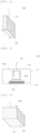
- the film-forming part 140 is provided with a nozzle 150 for supplying a mist to the substrate 110, as shown in FIG. 3 .
- An example of the nozzle 150 is shown in FIG. 4 .
- the nozzle 150 has a connection 151 connecting the nozzle 150 to the conveying part 109, and an opening surface 152 of the nozzle for spraying the mist.
- the position at which the nozzle 150 is provided is not particularly limited.
- the substrate 110 may be installed on the bottom surface of the film-forming chamber 107 and the nozzle 150 may be installed vertically above the substrate to be face up.
- the substrate 110 may be installed on the top surface of the film-forming chamber 107 and the nozzle 150 may be installed vertically below the substrate to be face down.
- the number of the nozzle and the opening surface of the nozzle is not particularly limited and may be any number of the nozzles and the opening surfaces of the nozzles if they have one or more. As shown in FIG. 5 , a plurality of nozzles 150a and 150b are provided, and as shown in FIG. 6 , the nozzles 150c may have a plurality of opening surfaces.
- the angle formed by the plane including the opening surface 152 of the nozzle and the plane including the substrate 110 is not particularly limited. As shown in FIG. 7 , a nozzle 150d including the opening surface 152 of the nozzle inclined to facilitate the mist flow in a specific direction may be provided. As shown in FIG. 8 , a nozzle 150e inclined a part of the opening surface of the nozzle may be provided. However, the substrate 110 and the opening surface of the nozzle are preferably parallel, as shown in FIG. 4 , as the film-formation with a simpler structure, fewer pits, and excellent smoothness can be performed.
- the film-forming part 140 may be also provided with a position adjustment mechanism (not shown) to allow the longest distance H [cm] among distances between points in the opening surface 152 of the nozzle and the surface of the substrate 110 to be adjusted as appropriate, to the extent described below.
- the nozzle 150 may be a structure assembled from a plurally of members such that the area of the opening surface of the nozzle can be adjusted as appropriate by adjusting the size of the members.
- the shape of the opening surface 152 of the nozzle is not particularly limited. Although it may be polygonal, circular, elliptical, etc., it is preferably square, and more preferably rectangular.
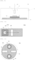
- the film-forming part 140 can be provided with a moving mechanism 160 moving the substrate 110 below the nozzle 150.
- the direction in which the substrate is moved is not particularly limited.
- a view of the film-forming part 140 with the moving mechanism 160a and 160b viewed from vertically above the substrate 110 is shown in FIGs. 10 and 11 .
- the substrate can also be rotated on its own axis with a mechanism that allows the substrate to rotate on its own axis.
- the speed at which the substrate is moved and the moving range are not particularly limited.
- the number of times per minute that one substrate passes under the nozzle may be 0.1 times or more, preferably 0.5 times or more, and more preferably 1 time or more.
- the number of times being 0.1 or more leads to be no areas where more gas is locally supplied (i.e., SH/Q does not decrease locally), resulting in the film having no increased pits and good surface smoothness.
- the upper limit of the number of times is not particularly limited, 120 times or less is good, preferably 60 times or less because as the number of times increases, the substrate fixation becomes unstable due to inertial forces.
- v/D may be 0.1/min or more, preferably 0.5/min or more to 120/min or less, and more preferably 1 to 60/min.
- D is not particularly limited, the diameter of the substrate R [mm] or more (100 mm or more for 4 inches, for example) is preferable.
- the upper limit of D is not particularly limited, the larger it is, the more films can be formed on a large number of substrates per nozzle.
- v is not particularly limited, it may be 10 mm/min or more to 30000 mm/min or less, preferably 30 mm/min or more to 12000 mm/min or less, more preferably 60 mm/min or more to 6000 mm/min or less.
- v is not particularly limited, it may be 10 mm/min or more to 30000 mm/min or less, preferably 30 mm/min or more to 12000 mm/min or less, more preferably 60 mm/min or more to 6000 mm/min or less.
- the rotatively moving mechanism as shown in FIG. 11 , it may be 0.1 rpm or more, preferably 0.5 to 120 rpm, and more preferably 1 to 60 rpm.
- an exhaust gas outlet 111 may be provided at a location that does not affect the supply of the mist to the substrate 110.
- the exhaust gas outlet 111 may be provided at one location or at two or more locations if not affecting the mist supply.
- the conveying part 109 connects the atomizing part 120 with the film-forming part 140.
- the mist is conveyed through the conveying part 109 from the mist generating source 104 of the atomizing part 120 to the nozzle 150 of the film-forming part 140 by means of the carrier gas.
- the conveying part 109 can be, for example, a supply pipe 109a.
- a quartz tube or a resin tube can be used as the supply tube 109a.
- the present invention is a film-forming method for heat-treating a raw material solution atomized into a mist and performing a film-formation, and the method includes the following steps: atomizing the raw material solution or making the raw material solution into droplets to generate a mist; conveying the mist to a film-forming part by a carrier gas; and supplying the mist from a nozzle to a substrate, heat-treating the mist on the substrate, and performing the film-formation in the film-forming part, wherein with the area of an opening surface of the nozzle being S [cm 2 ], the longest distance among distances between points in the opening surface and the surface of the substrate being H [cm], and the flow rate of the carrier gas supplied from the nozzle being Q [L/min], SH/Q ⁇ 0.015 results.
- the raw material solution 104a is atomized or the raw material solution 104a is made into droplets to generate a mist.
- This step can be performed using the atomizing part 120 as described above.
- the raw material solution (aqueous solutions) 104a is not particularly limited and may be any raw material solutions (aqueous solutions) 104a containing a material, which may be an inorganic or organic material that can be atomized into a mist.
- a material solution containing metal or metal compounds is suitable for the raw material solution.
- the raw material solution containing one or more metal selected from gallium, iron, indium, aluminum, vanadium, titanium, chromium, rhodium, nickel, and cobalt can be used.
- the raw material solution containing gallium is particularly preferred, and thus gallium-containing film with suppressed pits and good smoothness can be formed.
- the raw material solution is not particularly limited and may be any raw material solutions that can atomize the above metal (compound) into a mist
- the metal can be dissolved or dispersed in an organic solvent or water in the form of a complex or salt to suitably use as the raw material solution.
- complex forms include acetylacetonate complex, carbonyl complex, amine complex, hydride complex, etc.
- salt forms include metal chloride salt, metal bromide salt, and metal iodide salt.
- the above metal can be also dissolved in hydrobromic acid, hydrochloric acid, hydroiodic acid, etc. to use as an aqueous salt solution.
- a solute concentration is preferably 0.01 to 1 mol/L.
- the raw material solution containing halogen is particularly preferred as it suppresses the pits more and enables the film-formation with better smoothness.
- the raw material solution may be mixed with additives such as hydrohalic acid or oxidant.
- hydrohalic acid include hydrobromic acid, hydrochloric acid, and hydroiodic acid. Among these, hydrobromic acid or hydroiodic acid is preferred.
- oxidants include peroxide such as hydrogen peroxide (H 2 O 2 ), sodium peroxide (Na 2 O 2 ), barium peroxide (BaO 2 ), benzoyl peroxide (C 6 H 5 CO) 2 O 2 , and organic peroxide such as hypochlorous acid (HClO), perchloric acid, nitric acid, ozone water, peracetic acid or nitrobenzene.
- the raw material solution may contain dopants.
- dopants include, but not particularly limited to, n- type dopants such as tin, germanium, silicon, titanium, zirconium, vanadium or niobium, or p-type dopants such as copper, silver, tin, iridium or rhodium.
- concentration of dopants may be, for example, about 1.0 ⁇ 10 -9 to 1.0 mol/L, and may be as low as about 1.0 ⁇ 10 -7 mol/L or less, or as high as about 0.01 mol/L or more.
- the type of carrier gas is not particularly limited, and the carrier gas can be selected appropriately depending on the film-forming object.
- carrier gases include an inert gas such as oxygen, ozone, nitrogen or argon, or a reducing gas such as hydrogen gas or forming gas.
- a dilution gas diluted (e.g., diluted 10 times) the same gas as a first carrier gas with the other gas may be further used as a second carrier gas, or air can be used.
- the flow rate Q [L/min] of the carrier gas according to the present invention represents the total flow rate of the carrier gas.
- Q is the total flow rate of the carrier gas and the carrier gas for dilution. Note that Q is the measured value at 20°C. If the gas is measured at the other temperatures or at different types of flow rates (mass flow rate, etc.), it can be converted to a volumetric flow rate at 20°C using equation of state of gas.
- the flow rate is not particularly limited and may be any flow rates of the carrier gas (the total flow rates if multiple types of gases are used) that meet the conditions described below.
- the flow rate when performing the film-formation on the substrate with a diameter of 4 inches (100 mm), it is preferable to be the flow rate of 1 to 80 L/min, and 4 to 40 L/min is more preferable.
- SH/Q may be 0.015 or more, preferably 0.1 or more to 20 or less. If SH/Q is less than 0.015, the film has many pits and the surface of the film is not smooth.
- the speed of the carrier gas in the direction orthogonal to the substrate at the opening surface 152 of the nozzle may be between 0.01 m/s or more and less than 8.0 m/s, preferably between 0.1 m/s or more and less than 2.5 m/s.
- the area S of the opening surface 152 of the nozzle may be between 0.1 cm 2 or more and less than 400 cm 2 .
- the minimum distance H between the opening surface 152 of the nozzle and the substrate 110 is preferably between 0.1 cm or more and 6.0 cm or less, more preferably between 0.2 cm or more and 3.0 cm or less.
- S/A ⁇ 0.3 is preferable, more preferably 0.004 ⁇ S/A ⁇ 0.15.
- S/A ⁇ 0.3 allows the film to have fewer pits and better surface smoothness.
- the area A of the substrate is preferably 10 cm 2 or more. If the substrate is circular, the diameter is preferably 2 inches (50 mm) or more, as the film with good surface smoothness can be formed on the larger area.
- the upper limit of A is not particularly limited. The larger area of the substrate, the larger area of the film can be achieved in a single film-formation, and thus it is suitable for mass production.
- L/R ⁇ 1 is preferable.
- L/R ⁇ 1 a film having good smoothness can be easily formed on a large area of the substrate.
- the long axis refers to the long side of a rectangle.
- the upper limit of L/R is not particularly limited, it is preferably 3 or less, as the larger L/R is, the more mist is not supplied to the substrate.
- Heat-treatment is sufficient if the mist reacts by heating, and the reaction conditions, etc. are also not particularly limited.
- the heat-treatment can be set appropriately according to the raw material or the film-forming object.
- the heating temperature can be in the range of 120 to 600°C, preferably in the range of 200°C to 600°C, and more preferably in the range of 300°C to 550°C.
- the heating temperature being T [°C]
- the area of the opening surface 152 of the nozzle being S [cm 2 ]
- the flow rate of the carrier gas being Q [L/min]
- ST/Q is preferably 40 or more, more preferably between 100 or more and 2000 or less.
- ST/Q ⁇ 40 allows the film to have further fewer pits and even better surface smoothness.
- the heat-treatment may be performed under any atmosphere such as vacuum, non-oxygen atmosphere, reducing gas atmosphere, air atmosphere, and oxygen atmosphere, and can be set as appropriate according to the film-forming object.
- the reaction pressure may be under any conditions such as atmospheric, pressurized, or depressurized conditions.
- the film-formation under atmospheric pressure is preferred to allow to simplify the apparatus configuration.
- the substrate 110 is not particularly limited and may be any substrate 110 that is capable of performing the film-forming and supporting the film.
- a material of the substrate 110 is also not particularly limited, and any known substrates can be used, which may be an organic compound or an inorganic compound.
- the materials of the substrate 110 include, but are not limited to, polysulfone, polyether sulfone, polyphenylene sulfide, polyetheretherketone, polyimide, polyetherimide, fluororesin, metals such as iron, aluminum, stainless steel, and gold, silicon, sapphire, quartz, glass, gallium oxide, lithium niobate, lithium tantalate, etc.
- the thickness of the substrate is not particularly limited, it is preferably 10 to 2000 ⁇ m, and more preferably 50 to 800 ⁇ m.
- the film-formation may be performed directly on the substrate or may be stacked on an intermediate layer formed on the substrate.
- the intermediate layer is not particularly limited.
- the intermediate layer can include any of oxides containing aluminum, titanium, vanadium, chromium, iron, gallium, rhodium, indium, or iridium as main component.
- the metal oxides are Al 2 O 3 , Ti 2 O 3 , V 2 O 3 , Cr 2 O 3 , Fe 2 O 3 , Ga 2 O 3 , Rh 2 O 3 , In 2 O 3 , Ir 2 O 3 , and can be the metal oxide in a binary system represented by (A x B 1-x ) 2 O 3 (0 ⁇ x ⁇ 1) when two elements selected from the above metal elements are A and B or the metal oxide in a ternary system represented by (A x B y C 1-x-y ) 2 O 3 (0 ⁇ x ⁇ 1, 0 ⁇ y ⁇ 1, 0 ⁇ x+y ⁇ 1) when three elements selected from the above metal elements are A, B and C.
- an anneal treatment may be performed after film-forming.
- temperatures for the anneal treatment is, but not particularly limited to, preferably 600°C or less, and more preferably 550°C or less. This is because the crystallinity of the film is not impaired.
- the processing time of the anneal treatment is not particularly limited, it is preferably 10 seconds to 10 hours, and more preferably 10 seconds to 1 hour.
- the substrate 110 may be delaminated from the oxide semiconductor film.
- the delaminating method is not particularly limited, and may be any known methods. Examples of methods include a delaminating method by mechanical impact, applying heat and using thermal stress, applying vibration such as ultrasonic waves, etching, laser lift-off, etc. The delamination enables to obtain the oxide semiconductor film as a freestanding film.
- Electrode materials include metals such as Al, Ag, Ti, Pd, Au, Cu, Cr, Fe, W, Ta, Nb, Mn, Mo, Hf, Co, Zr, Sn, Pt, V, Ni, Ir, Zn, In, and Nd, as well as conductive metal oxide films such as tin oxide, zinc oxide, indium oxide, indium tin oxide (ITO), zinc indium oxide (IZO), or organic conductive compounds such as polyaniline, polythiophene, or polypyrrole. Any of the above electrode materials may be used. Alloys or mixtures of two or more of these materials may be used.
- the thickness of the electrode is preferably 1 to 1000 nm, more preferably 10 to 500 nm.
- the present invention is a film-forming system for heat-treating a raw material solution atomized into a mist and performing a film-formation, and the system comprises: a mechanism for atomizing the raw material solution or making the raw material solution into droplets to generate a mist; a mechanism for conveying the mist to a film-forming part by a carrier gas; and a mechanism for supplying the mist from a nozzle to a substrate, heat-treating the mist on the substrate, and performing the film-formation in the film-forming part, wherein with the area of an opening surface of the nozzle being S [cm 2 ], the longest distance among distances between points in the opening surface and the surface of the substrate being H [cm], and the flow rate of the carrier gas supplied from the nozzle being Q [L/min], SH/Q ⁇ 0.015 results.
- the raw material solution 104a is atomized or the raw material solution 104a is made into droplets to generate a mist.
- This mechanism can be performed using the atomizing part 120 as described above.
- the raw material solution (aqueous solution) 104a is not particularly limited and may be any raw material solutions (aqueous solutions) 104a containing a material, which may be an inorganic or organic material that can be atomized into a mist.
- a material solution containing metal or metal compounds is suitable for the raw material solution.
- the raw material solution containing one or more metal selected from gallium, iron, indium, aluminum, vanadium, titanium, chromium, rhodium, nickel, and cobalt can be used.
- the raw material solution containing gallium are particularly preferred, and thus gallium-containing film with suppressed pits and good smoothness can be formed.
- the raw material solution is not particularly limited and may be any raw material solutions that can atomize the above metal (compound) into a mist.
- the metal can be dissolved or dispersed in an organic solvent or water in the form of a complex or salt to suitably use as the raw material solution.
- complex forms include acetylacetonate complex, carbonyl complex, amine complex, hydride complex, etc.
- salt forms include metal chloride salt, metal bromide salt, and metal iodide salt.
- the above metal can be also dissolved in hydrobromic acid, hydrochloric acid, hydroiodic acid, etc. to use as an aqueous salt solution.
- a solute concentration is preferably 0.01 to 1 mol/L.
- the raw material solution containing halogen is particularly preferred as it suppresses the pits more and enables the film-formation having better smoothness.
- the raw material solution may be mixed with additives such as hydrohalic acid or oxidant.
- hydrohalic acid include hydrobromic acid, hydrochloric acid, and hydroiodic acid. Among these, hydrobromic acid or hydroiodic acid is preferred.
- oxidants include peroxide such as hydrogen peroxide (H 2 O 2 ), sodium peroxide (Na 2 O 2 ), barium peroxide (BaO 2 ), benzoyl peroxide (C 6 H 5 CO) 2 O 2 , and organic peroxide such as hypochlorous acid (HClO), perchloric acid, nitric acid, ozone water, peracetic acid or nitrobenzene.
- the raw material solution may contain dopants.
- dopants include, but not particularly limited to, n- type dopants such as tin, germanium, silicon, titanium, zirconium, vanadium or niobium, or p-type dopants such as copper, silver, tin, iridium or rhodium.
- concentration of dopants may be, for example, about 1.0 ⁇ 10 -9 to 1.0 mol/L, and may be as low as about 1.0 ⁇ 10 -7 mol/L or less, or as high as about 0.01 mol/L or more.
- the type of the carrier gas is not particularly limited, and the carrier gas can be selected appropriately depending on the film-forming object.
- carrier gases include an inert gas such as oxygen, ozone, nitrogen or argon, or a reducing gas such as hydrogen gas or forming gas.
- carrier gases include an inert gas such as oxygen, ozone, nitrogen or argon, or a reducing gas such as hydrogen gas or forming gas.
- a dilution gas diluted (e.g., diluted 10 times) the same gas as a first carrier gas with the other gas, may be further used as a second carrier gas, or air can be used.
- the flow rate Q [L/min] of the carrier gas according to the present invention represents the total flow rate of the carrier gas.
- Q is the total flow rate of the carrier gas and the carrier gas for dilution. Note that Q is the measured value at 20°C. If the gas is measured at the other temperatures or at different types of flow rates (mass flow rate, etc.), it can be converted to a volumetric flow rate at 20°C using equation of state of gas.
- the flow rate is not particularly limited and may be any flow rates of the carrier gas (the total flow rates if multiple types of gases are used) that meet the conditions described below.
- the flow rate when performing the film-formation on the substrate with a diameter of 4 inches (100 mm), it is preferable to use the flow rate of 1 to 80 L/min, and 4 to 40 L/min is more preferable.
- SH/Q may be 0.015 or more, preferably 0.1 or more to 20 or less. If SH/Q is less than 0.015, the film has many pits and the surface of the film is not smooth.
- the speed of the carrier gas in the direction orthogonal to the substrate at the opening surface 152 may be between 0.01 m/s or more and less than 8.0 m/s, preferably between 0.1 m/s or more and less than 2.5 m/s.
- the area S of the opening surface 152 of the nozzle may be between 0.1 cm 2 or more and less than 400 cm 2 .
- the minimum distance H between the opening surface 152 of the nozzle and the substrate 110 is preferably between 0.1 cm or more and 6.0 cm or less, more preferably between 0.2 cm or more and 3.0 cm or less.
- S/A ⁇ 0.3 is preferable, more preferably 0.004 ⁇ S/A ⁇ 0.15.
- S/A ⁇ 0.3 allows the film to have fewer pits and better surface smoothness.
- the area A of the substrate is preferably 10 cm 2 or more. If the substrate is circular, the diameter is preferably 2 inches (50 mm) or more, as the film having good surface smoothness can be formed on the larger area.
- the upper limit of A is not particularly limited. The larger the area of the substrate, the larger area of the film can be achieved in a single film-formation, and thus it is suitable for mass production.
- L/R ⁇ 1 is preferable.
- L/R ⁇ 1 a film having good smoothness can be easily formed on a large area of the substrate.
- the long axis refers to the long side of a rectangle.
- the upper limit of L/R is not particularly limited, it may be preferably 3 or less, as the larger L/R is, the more mist is not supplied to the substrate.
- the heating temperature can be set appropriately according to the raw materials or the film-forming object.
- the heating temperature can be in the range of 120 to 600°C, preferably in the range of 200°C to 600°C, and more preferably in the range of 300°C to 550°C.
- the heating temperature being T [°C]
- the area of the opening surface 152 of the nozzle being S [cm 2 ]
- the flow rate of the carrier gas being Q [L/min]
- ST/Q is preferably 40 or more, more preferably between 100 or more and 2000 or less.
- ST/Q ⁇ 40 allows the film to have further fewer pits and even better surface smoothness.
- the heat-treatment may be performed under any atmosphere such as vacuum, non-oxygen atmosphere, reducing gas atmosphere, air atmosphere, and oxygen atmosphere, and can be set as appropriate according to the film-forming object.
- the reaction pressure may be under any conditions such as atmospheric, pressurized, or depressurized conditions.
- the film-formation under atmospheric pressure is preferred to allow to simplify the apparatus configuration.
- the substrate 110 is not particularly limited and may be any substrate 110 that is capable of performing the film-formation and supporting the film.
- a material of the substrate 110 is also not particularly limited, and any known substrates can be used, which may be an organic compound or an inorganic compound.
- the materials of the substrate 110 include, but are not limited to, polysulfone, polyether sulfone, polyphenylene sulfide, polyetheretherketone, polyimide, polyetherimide, fluororesin, metals such as iron, aluminum, stainless steel, and gold, silicon, sapphire, quartz, glass, gallium oxide, lithium niobate, lithium tantalate, etc.
- the thickness of the substrate is not particularly limited, it is preferably 10 to 2000 ⁇ m, and more preferably 50 to 800 ⁇ m.
- the film-formation may be performed directly on the substrate or may be stacked on an intermediate layer formed on the substrate.
- the intermediate layer is not particularly limited.
- the intermediate layer can include any of oxides containing aluminum, titanium, vanadium, chromium, iron, gallium, rhodium, indium, or iridium as main component.
- the metal oxides are Al 2 O 3 , Ti 2 O 3 , V 2 O 3 , Cr 2 O 3 , Fe 2 O 3 , Ga 2 O 3 , Rh 2 O 3 , In 2 O 3 , Ir 2 O 3 , and can be the metal oxide in a binary system represented by (A x B 1-x ) 2 O 3 (0 ⁇ x ⁇ 1) when two elements selected from the above metal elements are A and B or the metal oxide in a ternary system represented by (A x B y C 1-x-y ) 2 O 3 (0 ⁇ x ⁇ 1, 0 ⁇ y1, 0 ⁇ x+y ⁇ 1) when three elements selected from the above metal elements are A, B and C.
- an anneal treatment may be performed after film-forming.
- temperatures for the anneal treatment is, but not particularly limited to, preferably 600°C or less, and more preferably 550°C or less. This is because the crystallinity of the film is not impaired.
- the processing time of the anneal treatment is not particularly limited, it is preferably 10 seconds to 10 hours, and more preferably 10 seconds to 1 hour.
- the substrate 110 may be delaminated from the oxide semiconductor film.
- the delaminating method is not particularly limited, and may be any known methods. Examples of methods include a delaminating method by mechanical impact, applying heat and using thermal stress, applying vibration such as ultrasonic waves, etching, laser lift-off, etc. The delamination enables to obtain the oxide semiconductor film as a freestanding film.
- Electrode materials include metals such as Al, Ag, Ti, Pd, Au, Cu, Cr, Fe, W, Ta, Nb, Mn, Mo, Hf, Co, Zr, Sn, Pt, V, Ni, Ir, Zn, In, and Nd, as well as conductive metal oxide films such as tin oxide, zinc oxide, indium oxide, indium tin oxide (ITO), zinc indium oxide (IZO), or organic conductive compounds such as polyaniline, polythiophene, or polypyrrole. Any of the above electrode materials may be used. Alloys or mixtures of two or more of these materials may be also used.
- the thickness of the electrode is preferably 1 to 1000 nm, more preferably 10 to 500 nm.
- Tin chloride was mixed with 0.05 mol/L gallium iodide aqueous solution to prepare an aqueous solution so that an atomic ratio of tin to gallium is 1 to 0.08, which was used as the raw material solution 104a.
- the raw material solution 104a obtained as described above was contained into the mist generating source 104. In this time, the temperature of the solution was 25°C.
- c-face sapphire substrate with 4 inches (100 mm diameter) was placed on the hot plate 108 in the film-forming chamber 107 as the substrate 110, and the hot plate 108 was operated to raise the temperature to 500°C.
- flow control valves 103a and 103b were opened to supply nitrogen gas as a carrier gas from the carrier gas sources 102a and 102b into the film-forming chamber 107 to fully replace the atmosphere of the film-forming chamber 107 by means of the carrier gas, as well as the flow rates of the main carrier gas and the carrier gas for dilution were adjusted to 12 L/min, respectively.
- the ultrasonic wave vibration 106 was vibrated at 2.4 MHz, and the vibration was propagated through the water 105a to the raw material solution 104a, and thereby the raw material solution 104a was atomized to generate a mist.
- This mist was supplied to the substrate 110 through the supply pipe 109a and the nozzle 150 by means of the carrier gas.
- the mist was heat-treated in the film-forming chamber 107 at 500°C under atmospheric pressure to form a thin film containing the gallium oxide ( ⁇ -Ga 2 O 3 ) having the corundum structure on the substrate 110.
- the film-forming time was set at 30 minutes.
- the substrate was moved back and forth by the moving mechanism as shown in FIG. 10 , so that the substrate and the hot plate passed under the nozzle once per minute at a speed of 15 cm/min.
- an n- semiconductor film was stacked as a second layer on the n+ semiconductor film obtained as described above under the same conditions using the same raw material solution as described above except that it did not contain tin chloride.
- the film-formation was performed in the same manner as in Example 1, except that the concentration of the raw material solution was changed to 0.3 mol/L, the area S of the opening surface of the nozzle was changed to 1.2 cm 2 , the longest distance H among distances between points in the opening surface 152 of the nozzle and the surface of the substrate 110 was changed to 2.5 cm, and the total flow rate of the carrier gas was changed to 14 L/min in total.
- the film-formation was performed in the same manner as in Example 1, except that a sapphire substrate with 6-inch (150 mm diameter) was used as the substrate 110, the area S of the opening surface of the nozzle was changed to 8.5 cm 2 , the longest distance H among distances between points in the opening surface 152 of the nozzle and the surface of the substrate 110 was changed to 0.2 cm, and the total flow rate of the carrier gas was changed to 36 L/min in total.
- the surface of the film after film-forming was observed using an optical microscope, and the number of pits within 0.01 to 1 cm 2 were counted.
- the pit density calculated by dividing the counted number of the pits part by the observed area was shown in Table 1.
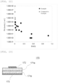
- the plotted results of the pit density against SH/Q are shown in FIG. 12 .
- a Pt layer, a Ti layer, and an Au layer were each stacked by electron beam evaporation to form a Schottky electrode 172.
- a Ti layer and an Au layer were each stacked by electron beam evaporation to form an ohmic electrode 173.
- the resulting semiconductor apparatus was evaluated for current-voltage characteristics.
- the voltage at which a dielectric breakdown occurs was examined by measuring the current-voltage characteristics in the reverse direction.
- FIG. 14 shows the yield plotted against the pit density calculated in Test Example 1.
- Table 1 Raw material Opening shape Conveyance SH/Q ST/Q S/A L/R Pit density [/cm 2 ] Yield [%] Ex. 1 GaI 3 rectangle reciprocating 0.5 125 0.076 1.2 ⁇ 1 98 Ex. 2 GaI 3 rectangle reciprocating 0.54 14 9 0.150 1.2 ⁇ 1 98 Ex. 3 GaI 3 rectangle reciprocating 1.08 270 0.150 1. 2 4 96 Ex. 4 GaI 3 rectangle reciprocating 0.54 135 0.150 1. 2 10 94 Ex. 5 GaI 3 rectangle reciprocating 0.21 42.9 0.015 1.2 41 90 Ex. 6 GaBr 3 rectangle reciprocating 0.14 42.9 0.015 1. 2 91 86 Ex.
- GaI 3 rectangle reciprocating 0.015 33.8 0.015 1.2 1.00E+04 10 Comp.
- Ex. 1 GaI 3 rectangle reciprocating 0.012 27 0.015 1.2 4.92E+04 3
- 2 GaI 3 rectangle reciprocating 0.01 22.5 0.015 1.2 1.14E+05 1
- 3 GaI 3 rectangle reciprocating 0.005 11.3 0.015 1.2 3.43E+06 0
Landscapes
- Chemical & Material Sciences (AREA)
- General Chemical & Material Sciences (AREA)
- Chemical Kinetics & Catalysis (AREA)
- Engineering & Computer Science (AREA)
- Materials Engineering (AREA)
- Mechanical Engineering (AREA)
- Metallurgy (AREA)
- Organic Chemistry (AREA)
- Dispersion Chemistry (AREA)
- Inorganic Chemistry (AREA)
- Crystals, And After-Treatments Of Crystals (AREA)
- Crystallography & Structural Chemistry (AREA)
- Liquid Deposition Of Substances Of Which Semiconductor Devices Are Composed (AREA)
- Formation Of Insulating Films (AREA)
- Chemical Vapour Deposition (AREA)
- Insulated Gate Type Field-Effect Transistor (AREA)
Abstract
Description
- The present invention relates to a film-forming method for performing a film-formation on a substrate using a mist-like raw material solution.
- A high-vacuum film-formation apparatus that can achieve non-equilibrium state, such as pulsed laser deposition (PLD), molecular beam epitaxy (MBE), and sputtering, have been developed, enabling to fabricate an oxide semiconductor that was previously impossible to fabricate using a conventional method such as a melt method. Mist chemical vapor deposition (hereinafter referred to as a mist CVD method) using the atomized mist-like raw material solution to grow crystal on a substrate, has also been developed, enabling to fabricate a gallium oxide (α-Ga2O3) having a corundum structure. As a semiconductor with a large band gap, α-Ga2O3 is expected to be applied to next-generation switching device that can achieve high-voltage, low loss, and high heat resistance.
- With reference to the mist CVD method, Patent Document 1 describes a tubular furnace type mist CVD apparatus. Patent Document 2 describes a fine channel type mist CVD apparatus. Patent Document 3 describes a linear source type mist CVD apparatus. Patent Document 4 describes a mist CVD apparatus of a tubular furnace, which differs from the mist CVD apparatus described in Patent Document 1 in that a carrier gas is introduced into a mist generator.
Patent Document 5 describes a mist CVD apparatus in which a substrate is placed above a mist generator and a susceptor is a rotating stage mounted on a hot plate. -
- Patent Document 1:
JP H01-257337 A - Patent Document 2:
JP 2005-307238 A - Patent Document 3:
JP 2012-046772 A - Patent Document 4:
JP 5397794 B1 - Patent Document 5:
JP 2014-063973 A - Unlike the other CVD methods, the mist CVD method can perform a film-formation at relatively low temperatures, and it is also possible to fabricate a crystal structure of a metastable phase such as the corundum structure of α-Ga2O3. However, the present inventors found that when the film-formation is performed using the mist CVD method, pits are formed on a film surface, resulting in the film surface having poor surface smoothness. There is also a problem that a film including many pits causes the pits to be killer defect, resulting in dielectric breakdown of a semiconductor apparatus. In addition, removal of the pits by polishing is problematic due to increasing the number of processes in creating the semiconductor apparatus.
- The present invention has been made to solve the above-described problems. An object of the present invention to provide: a film having suppressed pits and good surface smoothness; and a film-forming method for performing a film-formation such a film.
- The present invention has been made to achieve the above object. The present invention provides an oxide semiconductor film including gallium as main component, the oxide semiconductor film having a corundum structure, wherein pits on the surface of the oxide semiconductor film are 10000 pits/cm2 or less.
- Such oxide semiconductor film is simply and inexpensively obtained, and moreover has excellent surface smoothness, allowing to use suitable for a semiconductor apparatus.
- In this case, the pits on the surface of the oxide semiconductor film can be 100 pits/cm2 or less.
- This further improves the surface smoothness and enables to use more suitable for the semiconductor apparatus.
- In this case, the oxide semiconductor film can have an area of 10 cm2 or more.
- This results in a large-area oxide semiconductor film having excellent surface smoothness that can be suitably used in the semiconductor apparatus.
- In this case, the pits on the surface of the oxide semiconductor film have an opening diameter of 10 nm to 10 µm and the pits have a depth of 10 nm to 10 pm.
- This results in a large-area oxide semiconductor film having further excellent surface smoothness that can be even more suitably used in the semiconductor apparatus.
- In this case, the semiconductor apparatus can include the above oxide semiconductor film.
- This results in the semiconductor apparatus having excellent characteristics.
- The present invention also provides a film-forming method for heat-treating a raw material solution atomized into a mist and performing a film-formation, the method includes the following steps:
- atomizing the raw material solution or making the raw material solution into droplets to generate mist;
- conveying the mist to a film-forming part by a carrier gas; and
- supplying the mist from a nozzle to a substrate, heat-treating the mist on the substrate, and performing the film-formation in the film-forming part,
- wherein with the area of an opening surface of the nozzle being S [cm2], the longest distance among distances between points in the opening surface and the surface of the substrate being H [cm], and the flow rate of the carrier gas supplied from the nozzle being Q [L/min], SH/Q≥0.015 results.
- According to such film-forming method, the pits on the surface are suppressed, and thus the film having good smoothness can be formed.
- In this case, the raw material solution can contain gallium.
- This enables to suppress the pits on the surface, and thus the gallium-containing film with good smoothness can be formed.
- In this case, the raw material solution can contain halogen.
- This enables to suppress the pits on the surface, and thus the film having better smoothness can be formed.
- In this case, with the temperature of the heat-treatment being T[°C], ST/Q≥40 can result.
- This enables further to suppress the pits on the surface, and thus the film having even better smoothness can be formed.
- In this case, the mist can be supplied to the substrate from the nozzle provided vertically above the substrate.
- This enables further to suppress the pits on the surface, and thus the film having even better smoothness can be formed.
- In this case, the substrate can be moved under the nozzle.
- This enables to form the film having fewer pits on the surface and good smoothness on a large-area.
- In this case, with the area of the surface of the substrate to be performed the film-formation being A [cm2], S/A≤0.3 can result.
- This enables to form the film having fewer pits on the surface and good smoothness on a large-area.
- In this case, the opening surface of the nozzle can be rectangular.
- This enables to form the film having fewer pits on the surface and good smoothness on a large-area.
- In this case, with the length of the long axis of the opening surface of the nozzle being L [cm] and the maximum length in the long axis direction of the nozzle within the surface of the substrate to be performed the film-formation being R [cm], L/R≥1 can result.
- This enables to simply form the film having fewer pits on the surface and good smoothness on a large-area.
- In this case, the area of the substrate can be 10 cm2 or more.
- This enables to form the film having fewer pits on the surface and good smoothness on a large-area.
- As described above, the oxide semiconductor film according to the present invention can reduce the pits, have the excellent smoothness on the surface, and can be used suitable for the semiconductor apparatus.
- In addition, the film-forming method according to the present invention allows to form the film having fewer pits on the surface and good smoothness by way of simple method in the mist CVD method.
-
-
FIG. 1 is a schematic block view illustrating an example of a film-forming apparatus used in the present invention. -
FIG. 2 is a view describing an example of an atomizing part used in the present invention. -
FIG. 3 is a view describing an example of a film-forming part used in the present invention. -
FIG. 4 is a view describing an example of a nozzle used in the present invention. -
FIG. 5 is a view describing an example of the film-forming part provided with a plurality of nozzles. -
FIG. 6 is a view describing an example of the nozzle provided with a plurality of opening surfaces. -
FIG. 7 is a view describing an example of the nozzle used in the present invention. -
FIG. 8 is a view describing an example of the nozzle used in the present invention. -
FIG. 9 is a view describing an example of a movement mechanism of the substrate used in the present invention. -
FIG. 10 is a view describing an example of the moving mechanism reciprocating under the nozzle. -
FIG. 11 is a view describing an example of a rotary moving mechanism moving under the nozzle in one direction. -
FIG. 12 is a view illustrating the results of a test example 1. -
FIG. 13 is a view describing a structure of the semiconductor apparatus created in a test example 2. -
FIG. 14 is a view illustrating the results of a test example 2. -
FIG. 15 is a view illustrating a pit. -
FIG. 16 is a view describing an example of an oxide semiconductor film according to the present invention. - As described above, there was a need to provide an oxide semiconductor film having fewer pits and excellent surface smoothness inexpensively, and to provide a method for producing an oxide semiconductor film having fewer pits and excellent surface smoothness which is formed in a manner with simple, inexpensive, and low-temperature process.
- The present inventors have earnestly studied the above problem and consequently found that, an oxide semiconductor film including gallium as main component, the oxide semiconductor film having a corundum structure, wherein pits on the surface of the oxide semiconductor film are 10000 pits/cm2 or less, can be simply and inexpensively obtained, has the excellent surface smoothness, and can be used suitably for a semiconductor apparatus. This finding has led to the completion of the present invention.
- The present inventors have earnestly studied the above problem and consequently found that, a film-forming method for heat-treating a raw material solution atomized into a mist and performing a film-formation, the method including the following steps: atomizing the raw material solution or making the raw material solution into droplets to generate a mist; conveying the mist to a film-forming part by a carrier gas; and supplying the mist from a nozzle to a substrate, heat-treating the mist on the substrate, and performing the film-formation in the film-forming part, wherein with the area of an opening surface of the nozzle being S [cm2], the longest distance among distances between points in the opening surface and the surface of the substrate being H [cm], and the flow rate of the carrier gas supplied from the nozzle being Q [L/min], SH/Q≥0.015 results, enables to form a film with fewer pits and good smoothness. This finding has led to the completion of the present invention.
- Hereinafter, the present invention will be described in detail. However, the present invention is not limited thereto.
- Hereinafter, the present invention will be described with reference to the drawings.
- An oxide semiconductor film according to the present invention includes gallium as main component, and has a corundum structure, wherein pits on the surface of the oxide semiconductor film are 10000 pits/cm2 or less. While an oxide semiconductor film is typically composed of metal and oxygen, in the oxide semiconductor film according to the present invention, the metal contains gallium as main component. Herein, termed a main component means that 50 to 100% of the metal component is gallium. Termed a "gallium-based" means that the metal contains gallium as a metal component. Examples of metal components other than gallium may include one or more metals selected from iron, indium, aluminum, vanadium, titanium, chromium, rhodium, iridium, nickel, and cobalt.
- The pits are preferably less than 10000 pits/cm2, more preferably 100 pits/cm2 or less, and even more preferably less than 100 pits/cm2. Although a lower limit of the pits is not particularly limited, it may be 0.01 pits/cm2 or more.
- Dopants can be included in the oxide semiconductor film depending on the application. Examples of dopants include, but not particularly limited to, n- type dopants such as tin, germanium, silicon, titanium, zirconium, vanadium, or niobium, or p-type dopants such as copper, silver, tin, iridium, or rhodium. The concentration of dopants may be, for example, about 1.0×10¹⁶ to 1.0×10²²/cm3, and may be as low as about 1.0×10¹⁷/cm3 or less, or as high as about 1.0×10²⁰/cm3 or more.
- Herein, termed a pit in the present invention represents a recess formed on the film surface as shown in
FIG. 15 , and can be observed by an optical microscope, SEM, TEM, etc. The opening diameter of the pit is about 10 nm to 10 µm, and the depth of the pit is 10 nm to 10 pm. - Although the details of the reason for occurring pits are unknown, it is presumed that, when the velocity component of the mist in the direction orthogonal to the substrate is large and the weight (moisture content) of the mist at the point of arrival at the substrate is high, the impulse results in large when the mist collides the substrate, and causes an excessive amount of raw material component to be locally supplied and unreacted components or side-reactants in the mist to remain in the film. It is presumed that, the presence of such residues on the film surface leads the film to be less likely to grow locally. Therefore, it is presumed that, the conditions described hereafter can reduce the velocity component of the mist in the direction orthogonal to the substrate and the weight (moisture content) of the mist at the point of arrival at the substrate to reduce, thereby suppressing a pit-formation.
- In the oxide semiconductor film according to the present invention, the film thickness is not particularly limited. For example, it may be 0.05 to 100 µm, preferably 0.1 to 50 µm, and more preferably 0.5 to 20 pm.
- The
oxide semiconductor film 180 according to the present invention is formed on thesubstrate 181 as shown inFIG. 16 . - The other layer may be interposed between the
substrate 181 and theoxide semiconductor film 180. The other layer refers to a layer that differs in composition from thesubstrate 181 and the topmostoxide semiconductor film 180. It can be, for example, a crystalline oxide film, an insulating film, or a metal film. - The oxide semiconductor film preferably has an area of 10 cm2 or more, and if circular, a diameter of 2 inches (50 mm) or more is preferable. Although the upper limit of the area is not particularly limited, it is preferably 750 cm2 or less, and if circular, the diameter of 12 inches (300 mm) or less is preferable.
- The oxide semiconductor film according to the present invention can be used in a semiconductor apparatus by performing an appropriate structural design. The oxide semiconductor film can comprise the respective semiconductor layers for the semiconductor apparatus such as Schottky barrier diode (SBD), metal semiconductor field effect transistor (MESFET), high electron mobility transistor (HEMT), metal oxide film semiconductor field effect transistor (MOSFET), electrostatic induction transistor (SIT), junction field effect transistor (JFET), insulated gate type bipolar transistor (IGBT), light-emitting diode (LED).
-
FIG. 1 shows an example of a film-formingapparatus 101 that can be used for the film-forming method according to the present invention. The film-formingapparatus 101 has anatomizing part 120 atomizing a raw material solution into a mist to generate a mist, acarrier gas supplier 130 supplying a carrier gas to convey the mist, a film-formingpart 140 heat-treating the mist and performing the film-formation on a substrate, and a conveyingpart 109 connecting theatomizing part 120 with the film-formingpart 140 as well as conveying the mist by means of the carrier gas. The film-formingapparatus 101 may be also controlled by a control unit (not shown) controlling the entire or a part of the film-formingapparatus 101. - Herein, termed a mist in the present invention refers to a generic term for fine liquid particles dispersed in a gas, including those called mists, droplets, etc.
- In the
atomizing part 120, the raw material solution is atomized into a mist to generate a mist. An atomizing method is not particularly limited and may be any atomizing methods that the raw material solution can be atomized into a mist. Although any known atomizing methods can be used, it is preferable to use an atomizing method using ultrasonic wave vibration, as it can atomize the raw material solution into a mist more stably. - An example of
such atomizing part 120 is shown inFIG. 2 . For example, it may include amist generating source 104 in which theraw material solution 104a is contained, acontainer 105 in which a medium capable of transmitting ultrasonic wave vibration, forexample water 105a is contained, and anultrasonic wave vibration 106 attached to the bottom of thecontainer 105. Particularly, themist generating source 104 consisting of a container in which theraw material solution 104a is contained, is stored in thecontainer 105 in which thewater 105a is contained, using a support (not shown). Theultrasonic wave vibration 106 is provided on the bottom of thecontainer 105, and is connected to anoscillator 116. It is configured that when theoscillator 116 is activated, theultrasonic wave vibration 106 vibrates, and ultrasonic wave vibration propagates through thewater 105a into themist generating source 104 to atomize theraw material solution 104a into a mist. - The
carrier gas supplier 130 may have acarrier gas source 102a supplying the carrier gas, and include aflow control valve 103a to adjust the flow rate of the carrier gas delivered from thecarrier gas source 102a. It can also include a carrier gas source fordilution 102b supplying the carrier gas for dilution as needed, or aflow control valve 103b to adjust the flow rate of the carrier gas for dilution delivered from the carrier gas source fordilution 102b. There may be not only one but also two or more places for supplying the carrier gas. - In the film-forming
part 140, a mist is heated and heat-treated to perform the film-formation on a part or the entire of the surface of asubstrate 110. The film-formingpart 140 may or may not be partially or entirely enclosed in the film-formingpart 140. For example, as shown inFIG. 1 , the entire of the film-formingpart 140 may be enclosed to form a film-formingchamber 107. In the film-formingpart 140, thesubstrate 110 can be installed, and ahot plate 108 is provided for heating thesubstrate 110. Thehot plate 108 may be provided inside the film-formingchamber 107 as shown inFIG. 1 , or may be provided outside the film-formingchamber 107. It can also be provided with a movingstage 161a. The details are described below. - Furthermore, the film-forming
part 140 is provided with anozzle 150 for supplying a mist to thesubstrate 110, as shown inFIG. 3 . An example of thenozzle 150 is shown inFIG. 4 . Thenozzle 150 has aconnection 151 connecting thenozzle 150 to the conveyingpart 109, and anopening surface 152 of the nozzle for spraying the mist. The position at which thenozzle 150 is provided is not particularly limited. As shown inFIG. 3 , thesubstrate 110 may be installed on the bottom surface of the film-formingchamber 107 and thenozzle 150 may be installed vertically above the substrate to be face up. In contrast, thesubstrate 110 may be installed on the top surface of the film-formingchamber 107 and thenozzle 150 may be installed vertically below the substrate to be face down. - The number of the nozzle and the opening surface of the nozzle is not particularly limited and may be any number of the nozzles and the opening surfaces of the nozzles if they have one or more. As shown in
FIG. 5 , a plurality ofnozzles 150a and 150b are provided, and as shown inFIG. 6 , thenozzles 150c may have a plurality of opening surfaces. - The angle formed by the plane including the
opening surface 152 of the nozzle and the plane including thesubstrate 110 is not particularly limited. As shown inFIG. 7 , anozzle 150d including theopening surface 152 of the nozzle inclined to facilitate the mist flow in a specific direction may be provided. As shown inFIG. 8 , anozzle 150e inclined a part of the opening surface of the nozzle may be provided. However, thesubstrate 110 and the opening surface of the nozzle are preferably parallel, as shown inFIG. 4 , as the film-formation with a simpler structure, fewer pits, and excellent smoothness can be performed. - The film-forming
part 140 may be also provided with a position adjustment mechanism (not shown) to allow the longest distance H [cm] among distances between points in theopening surface 152 of the nozzle and the surface of thesubstrate 110 to be adjusted as appropriate, to the extent described below. - The
nozzle 150 may be a structure assembled from a plurally of members such that the area of the opening surface of the nozzle can be adjusted as appropriate by adjusting the size of the members. - The shape of the
opening surface 152 of the nozzle is not particularly limited. Although it may be polygonal, circular, elliptical, etc., it is preferably square, and more preferably rectangular. - As shown in
FIG. 9 , the film-formingpart 140 can be provided with a movingmechanism 160 moving thesubstrate 110 below thenozzle 150. The direction in which the substrate is moved is not particularly limited. A view of the film-formingpart 140 with the movingmechanism substrate 110 is shown inFIGs. 10 and 11 . There is a method for including the movingstage 161a on which thesubstrate 110 and thehot plate 108 are placed to move back and forth under thenozzle 150, as shown inFIG. 10 , or a method for rotatively moving thesubstrate 110 and thehot plate 108 under thenozzle 150 by a movingstage 161b on which thesubstrate 110 and thehot plate 108 are placed, as shown inFIG. 11 . In this case, the substrate can also be rotated on its own axis with a mechanism that allows the substrate to rotate on its own axis. - When providing the moving mechanism for the substrate, the speed at which the substrate is moved and the moving range are not particularly limited. However, the number of times per minute that one substrate passes under the nozzle may be 0.1 times or more, preferably 0.5 times or more, and more preferably 1 time or more. The number of times being 0.1 or more leads to be no areas where more gas is locally supplied (i.e., SH/Q does not decrease locally), resulting in the film having no increased pits and good surface smoothness. Although the upper limit of the number of times is not particularly limited, 120 times or less is good, preferably 60 times or less because as the number of times increases, the substrate fixation becomes unstable due to inertial forces.
- More specifically, in the case of the moving mechanism as shown in
FIG. 10 , with the moving speed of the substrate being v [mm/min] relative to the width of moving on the substrate D [mm], v/D may be 0.1/min or more, preferably 0.5/min or more to 120/min or less, and more preferably 1 to 60/min. Although D is not particularly limited, the diameter of the substrate R [mm] or more (100 mm or more for 4 inches, for example) is preferable. Although the upper limit of D is not particularly limited, the larger it is, the more films can be formed on a large number of substrates per nozzle. However, due to decrease of the film-forming speed per substrate, it is preferable to limit the number of substrates to be performed the film-formation per nozzle to 1000 mm or less for high productivity. Although v is not particularly limited, it may be 10 mm/min or more to 30000 mm/min or less, preferably 30 mm/min or more to 12000 mm/min or less, more preferably 60 mm/min or more to 6000 mm/min or less. In the case of the rotatively moving mechanism, as shown inFIG. 11 , it may be 0.1 rpm or more, preferably 0.5 to 120 rpm, and more preferably 1 to 60 rpm. - If the film-forming
part 140 is enclosed, anexhaust gas outlet 111 may be provided at a location that does not affect the supply of the mist to thesubstrate 110. Theexhaust gas outlet 111 may be provided at one location or at two or more locations if not affecting the mist supply. - The conveying
part 109 connects theatomizing part 120 with the film-formingpart 140. The mist is conveyed through the conveyingpart 109 from themist generating source 104 of theatomizing part 120 to thenozzle 150 of the film-formingpart 140 by means of the carrier gas. The conveyingpart 109 can be, for example, asupply pipe 109a. For example, a quartz tube or a resin tube can be used as thesupply tube 109a. - Then, a film-forming method according to the present invention will be described. The present invention is a film-forming method for heat-treating a raw material solution atomized into a mist and performing a film-formation, and the method includes the following steps: atomizing the raw material solution or making the raw material solution into droplets to generate a mist; conveying the mist to a film-forming part by a carrier gas; and supplying the mist from a nozzle to a substrate, heat-treating the mist on the substrate, and performing the film-formation in the film-forming part, wherein with the area of an opening surface of the nozzle being S [cm2], the longest distance among distances between points in the opening surface and the surface of the substrate being H [cm], and the flow rate of the carrier gas supplied from the nozzle being Q [L/min], SH/Q≥0.015 results.
- First, the
raw material solution 104a is atomized or theraw material solution 104a is made into droplets to generate a mist. This step can be performed using theatomizing part 120 as described above. Herein, the raw material solution (aqueous solutions) 104a is not particularly limited and may be any raw material solutions (aqueous solutions) 104a containing a material, which may be an inorganic or organic material that can be atomized into a mist. A material solution containing metal or metal compounds is suitable for the raw material solution. The raw material solution containing one or more metal selected from gallium, iron, indium, aluminum, vanadium, titanium, chromium, rhodium, nickel, and cobalt can be used. Among these, the raw material solution containing gallium is particularly preferred, and thus gallium-containing film with suppressed pits and good smoothness can be formed. - Although the raw material solution is not particularly limited and may be any raw material solutions that can atomize the above metal (compound) into a mist, the metal can be dissolved or dispersed in an organic solvent or water in the form of a complex or salt to suitably use as the raw material solution. Examples of complex forms include acetylacetonate complex, carbonyl complex, amine complex, hydride complex, etc. Examples of salt forms include metal chloride salt, metal bromide salt, and metal iodide salt. The above metal can be also dissolved in hydrobromic acid, hydrochloric acid, hydroiodic acid, etc. to use as an aqueous salt solution. A solute concentration is preferably 0.01 to 1 mol/L. Among these, the raw material solution containing halogen is particularly preferred as it suppresses the pits more and enables the film-formation with better smoothness.
- In addition, the raw material solution may be mixed with additives such as hydrohalic acid or oxidant. Examples of hydrohalic acid include hydrobromic acid, hydrochloric acid, and hydroiodic acid. Among these, hydrobromic acid or hydroiodic acid is preferred. Examples of oxidants include peroxide such as hydrogen peroxide (H2O2), sodium peroxide (Na2O2), barium peroxide (BaO2), benzoyl peroxide (C6H5CO)2O2, and organic peroxide such as hypochlorous acid (HClO), perchloric acid, nitric acid, ozone water, peracetic acid or nitrobenzene.
- Furthermore, the raw material solution may contain dopants. Examples of dopants include, but not particularly limited to, n- type dopants such as tin, germanium, silicon, titanium, zirconium, vanadium or niobium, or p-type dopants such as copper, silver, tin, iridium or rhodium. The concentration of dopants may be, for example, about 1.0×10⁻⁹ to 1.0 mol/L, and may be as low as about 1.0×10⁻⁷ mol/L or less, or as high as about 0.01 mol/L or more.
- Then, the generated mist is conveyed to the film-forming part by means of the carrier gas. The type of carrier gas is not particularly limited, and the carrier gas can be selected appropriately depending on the film-forming object. Examples of carrier gases include an inert gas such as oxygen, ozone, nitrogen or argon, or a reducing gas such as hydrogen gas or forming gas. One, two or more types of carrier gases may be used. For example, a dilution gas diluted (e.g., diluted 10 times) the same gas as a first carrier gas with the other gas, may be further used as a second carrier gas, or air can be used.
- The flow rate Q [L/min] of the carrier gas according to the present invention represents the total flow rate of the carrier gas. For example, if the carrier gas for dilution is used in addition to the carrier gas, Q is the total flow rate of the carrier gas and the carrier gas for dilution. Note that Q is the measured value at 20°C. If the gas is measured at the other temperatures or at different types of flow rates (mass flow rate, etc.), it can be converted to a volumetric flow rate at 20°C using equation of state of gas.
- The flow rate is not particularly limited and may be any flow rates of the carrier gas (the total flow rates if multiple types of gases are used) that meet the conditions described below. For example, when performing the film-formation on the substrate with a diameter of 4 inches (100 mm), it is preferable to be the flow rate of 1 to 80 L/min, and 4 to 40 L/min is more preferable.
- Then, in the film-forming part, the mist is supplied from the nozzle onto the substrate and heat-treated on the substrate to perform a film-formation. Herein, with the area of the
opening surface 152 of the nozzle being S [cm2], the flow rate of the carrier gas being Q [L/min], and the longest distance among distances between points in theopening surface 152 and the surface between thesubstrate 110 being H [cm], SH/Q may be 0.015 or more, preferably 0.1 or more to 20 or less. If SH/Q is less than 0.015, the film has many pits and the surface of the film is not smooth. In this case, the speed of the carrier gas in the direction orthogonal to the substrate at theopening surface 152 of the nozzle may be between 0.01 m/s or more and less than 8.0 m/s, preferably between 0.1 m/s or more and less than 2.5 m/s. - In this case, the area S of the
opening surface 152 of the nozzle may be between 0.1 cm2 or more and less than 400 cm2. The minimum distance H between the openingsurface 152 of the nozzle and thesubstrate 110 is preferably between 0.1 cm or more and 6.0 cm or less, more preferably between 0.2 cm or more and 3.0 cm or less. - With the area of the
opening surface 152 of the nozzle being S [cm2] and the area of the substrate being A [cm2], S/A≤0.3 is preferable, more preferably 0.004≤S/A≤0.15. S/A≤0.3 allows the film to have fewer pits and better surface smoothness. In this case, the area A of the substrate is preferably 10 cm2 or more. If the substrate is circular, the diameter is preferably 2 inches (50 mm) or more, as the film with good surface smoothness can be formed on the larger area. The upper limit of A is not particularly limited. The larger area of the substrate, the larger area of the film can be achieved in a single film-formation, and thus it is suitable for mass production. - It is preferable to use a nozzle with a rectangular opening surface. In this case, with the length of the long axis of the
opening surface 152 of the nozzle being L [cm] and the maximum length of the substrate in the direction of long axis of the nozzle being R [cm], L/R≥1 is preferable. With L/R≥1, a film having good smoothness can be easily formed on a large area of the substrate. Herein, the long axis refers to the long side of a rectangle. Although the upper limit of L/R is not particularly limited, it is preferably 3 or less, as the larger L/R is, the more mist is not supplied to the substrate. - Heat-treatment is sufficient if the mist reacts by heating, and the reaction conditions, etc. are also not particularly limited. The heat-treatment can be set appropriately according to the raw material or the film-forming object. For example, the heating temperature can be in the range of 120 to 600°C, preferably in the range of 200°C to 600°C, and more preferably in the range of 300°C to 550°C. With the heating temperature being T [°C], the area of the
opening surface 152 of the nozzle being S [cm2], and the flow rate of the carrier gas being Q [L/min], ST/Q is preferably 40 or more, more preferably between 100 or more and 2000 or less. ST/Q≥40 allows the film to have further fewer pits and even better surface smoothness. - The heat-treatment may be performed under any atmosphere such as vacuum, non-oxygen atmosphere, reducing gas atmosphere, air atmosphere, and oxygen atmosphere, and can be set as appropriate according to the film-forming object. In addition, the reaction pressure may be under any conditions such as atmospheric, pressurized, or depressurized conditions. However, the film-formation under atmospheric pressure is preferred to allow to simplify the apparatus configuration.
- The
substrate 110 is not particularly limited and may be anysubstrate 110 that is capable of performing the film-forming and supporting the film. A material of thesubstrate 110 is also not particularly limited, and any known substrates can be used, which may be an organic compound or an inorganic compound. Examples of the materials of thesubstrate 110 include, but are not limited to, polysulfone, polyether sulfone, polyphenylene sulfide, polyetheretherketone, polyimide, polyetherimide, fluororesin, metals such as iron, aluminum, stainless steel, and gold, silicon, sapphire, quartz, glass, gallium oxide, lithium niobate, lithium tantalate, etc. Although the thickness of the substrate is not particularly limited, it is preferably 10 to 2000 µm, and more preferably 50 to 800 µm. - The film-formation may be performed directly on the substrate or may be stacked on an intermediate layer formed on the substrate. The intermediate layer is not particularly limited. For example, the intermediate layer can include any of oxides containing aluminum, titanium, vanadium, chromium, iron, gallium, rhodium, indium, or iridium as main component. More specifically, the metal oxides are Al2O3, Ti2O3, V2O3, Cr2O3, Fe2O3, Ga2O3, Rh2O3, In2O3, Ir2O3, and can be the metal oxide in a binary system represented by (AxB1-x)2O3 (0<x<1) when two elements selected from the above metal elements are A and B or the metal oxide in a ternary system represented by (AxByC1-x-y)2O3 (0<x<1, 0<y<1, 0<x+y<1) when three elements selected from the above metal elements are A, B and C.
- In the present invention, an anneal treatment may be performed after film-forming. Examples of temperatures for the anneal treatment is, but not particularly limited to, preferably 600°C or less, and more preferably 550°C or less. This is because the crystallinity of the film is not impaired. Although the processing time of the anneal treatment is not particularly limited, it is preferably 10 seconds to 10 hours, and more preferably 10 seconds to 1 hour.
- The
substrate 110 may be delaminated from the oxide semiconductor film. The delaminating method is not particularly limited, and may be any known methods. Examples of methods include a delaminating method by mechanical impact, applying heat and using thermal stress, applying vibration such as ultrasonic waves, etching, laser lift-off, etc. The delamination enables to obtain the oxide semiconductor film as a freestanding film. - General method i.e., any of methods such as vapor deposition, sputtering, CVD, plating, as well as a printing method for adhering together with such as a resin can be used to form an electrode required to configure a semiconductor apparatus. Examples of electrode materials include metals such as Al, Ag, Ti, Pd, Au, Cu, Cr, Fe, W, Ta, Nb, Mn, Mo, Hf, Co, Zr, Sn, Pt, V, Ni, Ir, Zn, In, and Nd, as well as conductive metal oxide films such as tin oxide, zinc oxide, indium oxide, indium tin oxide (ITO), zinc indium oxide (IZO), or organic conductive compounds such as polyaniline, polythiophene, or polypyrrole. Any of the above electrode materials may be used. Alloys or mixtures of two or more of these materials may be used. The thickness of the electrode is preferably 1 to 1000 nm, more preferably 10 to 500 nm.
- Then, a film-forming system according to the present invention will be described. The present invention is a film-forming system for heat-treating a raw material solution atomized into a mist and performing a film-formation, and the system comprises: a mechanism for atomizing the raw material solution or making the raw material solution into droplets to generate a mist; a mechanism for conveying the mist to a film-forming part by a carrier gas; and a mechanism for supplying the mist from a nozzle to a substrate, heat-treating the mist on the substrate, and performing the film-formation in the film-forming part, wherein with the area of an opening surface of the nozzle being S [cm2], the longest distance among distances between points in the opening surface and the surface of the substrate being H [cm], and the flow rate of the carrier gas supplied from the nozzle being Q [L/min], SH/Q≥0.015 results.
- First, the
raw material solution 104a is atomized or theraw material solution 104a is made into droplets to generate a mist. This mechanism can be performed using theatomizing part 120 as described above. Herein, the raw material solution (aqueous solution) 104a is not particularly limited and may be any raw material solutions (aqueous solutions) 104a containing a material, which may be an inorganic or organic material that can be atomized into a mist. A material solution containing metal or metal compounds is suitable for the raw material solution. The raw material solution containing one or more metal selected from gallium, iron, indium, aluminum, vanadium, titanium, chromium, rhodium, nickel, and cobalt can be used. Among these, the raw material solution containing gallium are particularly preferred, and thus gallium-containing film with suppressed pits and good smoothness can be formed. - The raw material solution is not particularly limited and may be any raw material solutions that can atomize the above metal (compound) into a mist. The metal can be dissolved or dispersed in an organic solvent or water in the form of a complex or salt to suitably use as the raw material solution. Examples of complex forms include acetylacetonate complex, carbonyl complex, amine complex, hydride complex, etc. Examples of salt forms include metal chloride salt, metal bromide salt, and metal iodide salt. The above metal can be also dissolved in hydrobromic acid, hydrochloric acid, hydroiodic acid, etc. to use as an aqueous salt solution. A solute concentration is preferably 0.01 to 1 mol/L. Among these, the raw material solution containing halogen is particularly preferred as it suppresses the pits more and enables the film-formation having better smoothness.
- In addition, the raw material solution may be mixed with additives such as hydrohalic acid or oxidant. Examples of hydrohalic acid include hydrobromic acid, hydrochloric acid, and hydroiodic acid. Among these, hydrobromic acid or hydroiodic acid is preferred. Examples of oxidants include peroxide such as hydrogen peroxide (H2O2), sodium peroxide (Na2O2), barium peroxide (BaO2), benzoyl peroxide (C6H5CO)2O2, and organic peroxide such as hypochlorous acid (HClO), perchloric acid, nitric acid, ozone water, peracetic acid or nitrobenzene.
- Furthermore, the raw material solution may contain dopants. Examples of dopants include, but not particularly limited to, n- type dopants such as tin, germanium, silicon, titanium, zirconium, vanadium or niobium, or p-type dopants such as copper, silver, tin, iridium or rhodium. The concentration of dopants may be, for example, about 1.0×10⁻⁹ to 1.0 mol/L, and may be as low as about 1.0×10⁻⁷ mol/L or less, or as high as about 0.01 mol/L or more.
- Then, the generated mist is conveyed to the film-forming part by means of the carrier gas. This mechanism can be performed using the conveying
part 109 as described above. Herein, the type of the carrier gas is not particularly limited, and the carrier gas can be selected appropriately depending on the film-forming object. Examples of carrier gases include an inert gas such as oxygen, ozone, nitrogen or argon, or a reducing gas such as hydrogen gas or forming gas. One, two or more types of carrier gases may be used. For example, a dilution gas diluted (e.g., diluted 10 times) the same gas as a first carrier gas with the other gas, may be further used as a second carrier gas, or air can be used. - The flow rate Q [L/min] of the carrier gas according to the present invention represents the total flow rate of the carrier gas. For example, if carrier gas for dilution is used in addition to the carrier gas, Q is the total flow rate of the carrier gas and the carrier gas for dilution. Note that Q is the measured value at 20°C. If the gas is measured at the other temperatures or at different types of flow rates (mass flow rate, etc.), it can be converted to a volumetric flow rate at 20°C using equation of state of gas.
- The flow rate is not particularly limited and may be any flow rates of the carrier gas (the total flow rates if multiple types of gases are used) that meet the conditions described below. For example, when performing the film-formation on the substrate with a diameter of 4 inches (100 mm), it is preferable to use the flow rate of 1 to 80 L/min, and 4 to 40 L/min is more preferable.
- Then, in the film-forming
part 140, the mist is supplied from the nozzle onto the substrate and heat treated on said substrate to perform a film-formation. Herein, with the area of theopening surface 152 of the nozzle being S [cm2], the flow rate of the carrier gas being Q [L/min], and the longest distance among distances between points in theopening surface 152 and the surface between thesubstrate 110 being H [cm], SH/Q may be 0.015 or more, preferably 0.1 or more to 20 or less. If SH/Q is less than 0.015, the film has many pits and the surface of the film is not smooth. In this case, the speed of the carrier gas in the direction orthogonal to the substrate at theopening surface 152 may be between 0.01 m/s or more and less than 8.0 m/s, preferably between 0.1 m/s or more and less than 2.5 m/s. - In this case, the area S of the
opening surface 152 of the nozzle may be between 0.1 cm2 or more and less than 400 cm2. The minimum distance H between the openingsurface 152 of the nozzle and thesubstrate 110 is preferably between 0.1 cm or more and 6.0 cm or less, more preferably between 0.2 cm or more and 3.0 cm or less. - With the area of the
opening surface 152 of the nozzle being S [cm2] and the area of the substrate being A [cm2], S/A≤0.3 is preferable, more preferably 0.004≤S/A≤0.15. S/A≤0.3 allows the film to have fewer pits and better surface smoothness. In this case, the area A of the substrate is preferably 10 cm2 or more. If the substrate is circular, the diameter is preferably 2 inches (50 mm) or more, as the film having good surface smoothness can be formed on the larger area. The upper limit of A is not particularly limited. The larger the area of the substrate, the larger area of the film can be achieved in a single film-formation, and thus it is suitable for mass production. - It is preferable to use a nozzle with a rectangular opening surface. In this case, with the length of the long axis of the
opening surface 152 of the nozzle being L [cm] and the maximum length of the substrate in the direction of long axis of the nozzle being R [cm], L/R≥1 is preferable. With L/R≥1, a film having good smoothness can be easily formed on a large area of the substrate. Herein, the long axis refers to the long side of a rectangle. Although the upper limit of L/R is not particularly limited, it may be preferably 3 or less, as the larger L/R is, the more mist is not supplied to the substrate. - Heat-treatment is sufficient if the mist reacts by heating, and the reaction conditions, etc. are not particularly limited. The heating temperature can be set appropriately according to the raw materials or the film-forming object. For example, the heating temperature can be in the range of 120 to 600°C, preferably in the range of 200°C to 600°C, and more preferably in the range of 300°C to 550°C. With the heating temperature being T [°C], the area of the
opening surface 152 of the nozzle being S [cm2], and the flow rate of the carrier gas being Q [L/min], ST/Q is preferably 40 or more, more preferably between 100 or more and 2000 or less. ST/Q≥40 allows the film to have further fewer pits and even better surface smoothness. - The heat-treatment may be performed under any atmosphere such as vacuum, non-oxygen atmosphere, reducing gas atmosphere, air atmosphere, and oxygen atmosphere, and can be set as appropriate according to the film-forming object. In addition, the reaction pressure may be under any conditions such as atmospheric, pressurized, or depressurized conditions. However, the film-formation under atmospheric pressure is preferred to allow to simplify the apparatus configuration.
- The
substrate 110 is not particularly limited and may be anysubstrate 110 that is capable of performing the film-formation and supporting the film. A material of thesubstrate 110 is also not particularly limited, and any known substrates can be used, which may be an organic compound or an inorganic compound. Examples of the materials of thesubstrate 110 include, but are not limited to, polysulfone, polyether sulfone, polyphenylene sulfide, polyetheretherketone, polyimide, polyetherimide, fluororesin, metals such as iron, aluminum, stainless steel, and gold, silicon, sapphire, quartz, glass, gallium oxide, lithium niobate, lithium tantalate, etc. Although the thickness of the substrate is not particularly limited, it is preferably 10 to 2000 µm, and more preferably 50 to 800 µm. - The film-formation may be performed directly on the substrate or may be stacked on an intermediate layer formed on the substrate. The intermediate layer is not particularly limited. For example, the intermediate layer can include any of oxides containing aluminum, titanium, vanadium, chromium, iron, gallium, rhodium, indium, or iridium as main component. More specifically, the metal oxides are Al2O3, Ti2O3, V2O3, Cr2O3, Fe2O3, Ga2O3, Rh2O3, In2O3, Ir2O3, and can be the metal oxide in a binary system represented by (AxB1-x)2O3 (0<x<1) when two elements selected from the above metal elements are A and B or the metal oxide in a ternary system represented by (AxByC1-x-y)2O3 (0<x<1, 0<y1, 0<x+y<1) when three elements selected from the above metal elements are A, B and C.
- In the present invention, an anneal treatment may be performed after film-forming. Examples of temperatures for the anneal treatment is, but not particularly limited to, preferably 600°C or less, and more preferably 550°C or less. This is because the crystallinity of the film is not impaired. Although the processing time of the anneal treatment is not particularly limited, it is preferably 10 seconds to 10 hours, and more preferably 10 seconds to 1 hour.
- The
substrate 110 may be delaminated from the oxide semiconductor film. The delaminating method is not particularly limited, and may be any known methods. Examples of methods include a delaminating method by mechanical impact, applying heat and using thermal stress, applying vibration such as ultrasonic waves, etching, laser lift-off, etc. The delamination enables to obtain the oxide semiconductor film as a freestanding film. - General method i.e., any of methods such as vapor deposition, sputtering, CVD, plating, as well as a printing method for adhering together with a resin can be used to form the electrodes required to configure a semiconductor apparatus. Examples of electrode materials include metals such as Al, Ag, Ti, Pd, Au, Cu, Cr, Fe, W, Ta, Nb, Mn, Mo, Hf, Co, Zr, Sn, Pt, V, Ni, Ir, Zn, In, and Nd, as well as conductive metal oxide films such as tin oxide, zinc oxide, indium oxide, indium tin oxide (ITO), zinc indium oxide (IZO), or organic conductive compounds such as polyaniline, polythiophene, or polypyrrole. Any of the above electrode materials may be used. Alloys or mixtures of two or more of these materials may be also used. The thickness of the electrode is preferably 1 to 1000 nm, more preferably 10 to 500 nm.
- Hereinafter, the present invention will be specifically described with reference to Examples and Comparative Examples. However, the present invention is not limited thereto.
- In this example, the film-forming apparatus shown in
FIG. 1 was used. - Tin chloride was mixed with 0.05 mol/L gallium iodide aqueous solution to prepare an aqueous solution so that an atomic ratio of tin to gallium is 1 to 0.08, which was used as the
raw material solution 104a. Theraw material solution 104a obtained as described above was contained into themist generating source 104. In this time, the temperature of the solution was 25°C. - Then, c-face sapphire substrate with 4 inches (100 mm diameter) was placed on the
hot plate 108 in the film-formingchamber 107 as thesubstrate 110, and thehot plate 108 was operated to raise the temperature to 500°C. - Subsequently, flow
control valves carrier gas sources chamber 107 to fully replace the atmosphere of the film-formingchamber 107 by means of the carrier gas, as well as the flow rates of the main carrier gas and the carrier gas for dilution were adjusted to 12 L/min, respectively. - Then, the
ultrasonic wave vibration 106 was vibrated at 2.4 MHz, and the vibration was propagated through thewater 105a to theraw material solution 104a, and thereby theraw material solution 104a was atomized to generate a mist. - This mist was supplied to the
substrate 110 through thesupply pipe 109a and thenozzle 150 by means of the carrier gas. As thenozzle 150, the nozzle with a rectangular-shapedopening surface 152 was used, and the nozzle was adjusted so that with the area of theopening surface 152 of the nozzle being S [cm2], the flow rate of the carrier gas being Q [L/min], and the longest distance among distances between points in theopening surface 152 of the nozzle and the surface of thesubstrate 110 being H [cm], SH/Q=0.5 resulted. In this case, S=6.0, H=2.0, and Q=24. - Then, the mist was heat-treated in the film-forming
chamber 107 at 500°C under atmospheric pressure to form a thin film containing the gallium oxide (α-Ga2O3) having the corundum structure on thesubstrate 110. The film-forming time was set at 30 minutes. - With the heat-treatment temperature being set to T [°C], ST/Q=40 resulted, with the area of the substrate being set to A [cm2], S/A=0.024 resulted, and with the length of the long axis of the
opening surface 152 of the nozzle being set to L [cm] and the maximum length of the nozzle long axis direction of the substrate being R [cm], L/R=1.2 resulted. In this case, T=500, A=78.5, L=12, and R=10. - The substrate was moved back and forth by the moving mechanism as shown in
FIG. 10 , so that the substrate and the hot plate passed under the nozzle once per minute at a speed of 15 cm/min. - Subsequently, an n- semiconductor film was stacked as a second layer on the n+ semiconductor film obtained as described above under the same conditions using the same raw material solution as described above except that it did not contain tin chloride.
- The film-formation was performed in the same manner as in Example 1, except that the area S of the opening surface of the nozzle was changed to 10.8 cm2, the total flow rate of the carrier gas was changed to 40 L/min in total, and the film-forming temperature T was changed to 550°C. At this time, SH/Q=0.54, ST/Q=149, and S/A=0.15 resulted.
- The film-formation was performed in the same manner as in Example 2, except that the total flow rate of the carrier gas was changed to 20 L/min in total and the film-forming temperature T was changed to 500°C. At this time, SH/Q=1.08, ST/Q=270, and S/A=0.15 resulted.
- The film-formation was performed in the same manner as in Example 2, except that the film-forming temperature T was changed to 500°C. At this time, SH/Q=0.54, ST/Q=135, and S/A=0.15 resulted.
- The film-formation was performed in the same manner as in Example 1, except that the concentration of the raw material solution was changed to 0.3 mol/L, the area S of the opening surface of the nozzle was changed to 1.2 cm2, the longest distance H among distances between points in the
opening surface 152 of the nozzle and the surface of thesubstrate 110 was changed to 2.5 cm, and the total flow rate of the carrier gas was changed to 14 L/min in total. At this time, SH/Q=0.21, ST/Q=42.9, and S/A=0.015 resulted. - The film-formation was performed in the same manner as in Example 5, except that a 0.3 mol/L gallium bromide aqueous solution was used as the raw material solution, and the longest distance H among distances between points in the
opening surface 152 of the nozzle and the surface of thesubstrate 110 was changed to 1.6 cm, wherein SH/Q=0.14, ST/Q=42.9, and S/A=0.015 resulted. - The film-formation was performed in the same manner as in Example 1, except that a sapphire substrate with 6-inch (150 mm diameter) was used as the
substrate 110, the area S of the opening surface of the nozzle was changed to 8.5 cm2, the longest distance H among distances between points in theopening surface 152 of the nozzle and the surface of thesubstrate 110 was changed to 0.2 cm, and the total flow rate of the carrier gas was changed to 36 L/min in total. At this time, SH/Q=0.047, ST/Q=118, S/A=0.048, and L/R=1.1 resulted. - The film-formation was performed in the same manner as in Example 1, except that an aqueous solution with a 0.05 mol/L gallium acetylacetonate complex dissolved in water containing 1.5% hydrochloric acid by volume was used as the raw material solution, the area S of the opening surface of the nozzle was changed to 1.2 cm2, the longest distance H among distances between points in the
opening surface 152 of the nozzle and the surface of thesubstrate 110 was changed to 0.2 cm, the total flow rate of the carrier gas was changed to 10 L/min in total, and the film-forming temperature T was changed to 450°C. At this time, SH/Q=0.024, ST/Q=54, and S/A=0.015 resulted. - The film-formation was performed in the same manner as in Example 6, except that the longest distance H among distances between points in the
opening surface 152 of the nozzle and the surface of thesubstrate 110 was changed 1.2 cm. At this time, SH/Q=0.1, ST/Q=42.9, and S/A=0.015 resulted. - The film-formation was performed in the same manner as in Example 1, except that the area S of the opening surface of the nozzle was changed to 24 cm2, the longest distance H among distances between points in the
opening surface 152 of the nozzle and the surface of thesubstrate 110 was changed to 0.2 cm, the total flow rate of the carrier gas was changed to 80 L/min in total, and the film-forming temperature T was changed to 550°C. At this time, SH/Q=0.06, ST/Q=165, and S/A=0.30 resulted. - The film-formation was performed in the same manner as in Example 1, except that the area S of the opening surface of the nozzle was changed to 5.0 cm2, the longest distance H among distances between points in the
opening surface 152 of the nozzle and the surface of thesubstrate 110 was changed to 0.2 cm, the total flow rate of the carrier gas was changed to 60 L/min in total. At this time, SH/Q=0.017, ST/Q=41.7, S/A=0.064, and L/R=1.0 resulted. - The film-formation was performed in the same manner as in Example 1, except that the shape of the opening surface of the nozzle was circular with 4 inches (100 mm) in diameter, the longest distance H among distances between points in the
opening surface 152 of the nozzle and the surface of thesubstrate 110 was changed to 0.2 cm, the substrate was not moved, the flow rate of the carrier gas was changed to 80 L/min in total, and the heating temperature was 550°C. At this time, SH/Q=0.20, ST/Q=540, S/A=1, and L/R=1 resulted. - The film-formation was performed in the same manner as in Example 6, except that a 0.05 mol/L gallium bromide aqueous solution was used as the raw material solution and deuterium bromide was added 10% by volume, the longest distance H among distances between points in the
opening surface 152 of the nozzle and the surface of thesubstrate 110 was changed to 0.2 cm, and the film-forming temperature T was changed to 470°C. At this time, SH/Q=0.017, ST/Q=40, and S/A=0.015 resulted. - The film-formation was performed in the same manner as in Example 6, except that a gallium bromide aqueous solution with 0.05 mol/L was used as the raw material solution, the longest distance H among distances between points in the
opening surface 152 of the nozzle and the surface of thesubstrate 110 was changed to 0.2 cm, the total flow rate of the carrier gas was changed to 16 L/min in total, and the film-forming temperature T was changed to 450°C. At this time, SH/Q=0.015, ST/Q=33.8, and S/A=0.015 resulted. - The film-formation was performed in the same manner as in Example 14, except that the total flow rate of the carrier gas was changed to 20 L/min in total. At this time, SH/Q=0.012, ST/Q=27, and S/A=0.015 resulted.
- The film-formation was performed in the same manner as in Example 14, except that the total flow rate of the carrier gas was changed to 24 L/min in total. At this time, SH/Q=0.01, ST/Q=22.5, and S/A=0.015 resulted.
- The film-formation was performed in the same manner as in Example 14, except that the total flow rate of the carrier gas was changed to 48 L/min in total. At this time, SH/Q=0.005, ST/Q=11.3, and S/A=0.015 resulted.
- The film-formation was performed in the same manner as in Example 14, except that the total flow rate of the carrier gas was changed to 60 L/min in total. At this time, SH/Q=0.004, ST/Q=9, and S/A=0.015 resulted.
- The surface of the film after film-forming was observed using an optical microscope, and the number of pits within 0.01 to 1 cm2 were counted. The pit density calculated by dividing the counted number of the pits part by the observed area was shown in Table 1. The plotted results of the pit density against SH/Q are shown in
FIG. 12 . - Using the semiconductor film obtained as described above, a
semiconductor apparatus 170 as shown inFIG. 13 was created. - On a n-
type semiconductor layer 171a, a Pt layer, a Ti layer, and an Au layer were each stacked by electron beam evaporation to form aSchottky electrode 172. - On a n+
type semiconductor layer 171b, a Ti layer and an Au layer were each stacked by electron beam evaporation to form anohmic electrode 173. - The resulting semiconductor apparatus was evaluated for current-voltage characteristics. The voltage at which a dielectric breakdown occurs was examined by measuring the current-voltage characteristics in the reverse direction. The semiconductor apparatus with a withstand voltage of 300 V or higher was determined as accepted products, and the yield was calculated as the number of accepted products/the total number of created semiconductor apparatus=yield [%]. The results are shown in Table 1.
-
FIG. 14 shows the yield plotted against the pit density calculated in Test Example 1.[Table 1] Raw material Opening shape Conveyance SH/Q ST/Q S/A L/R Pit density [/cm2] Yield [%] Ex. 1 GaI3 rectangle reciprocating 0.5 125 0.076 1.2 <1 98 Ex. 2 GaI3 rectangle reciprocating 0.54 14 9 0.150 1.2 <1 98 Ex. 3 GaI3 rectangle reciprocating 1.08 270 0.150 1. 2 4 96 Ex. 4 GaI3 rectangle reciprocating 0.54 135 0.150 1. 2 10 94 Ex. 5 GaI3 rectangle reciprocating 0.21 42.9 0.015 1.2 41 90 Ex. 6 GaBr3 rectangle reciprocating 0.14 42.9 0.015 1. 2 91 86 Ex. 7 GaI3 rectangle reciprocating 0.047 118 0.048 1.1 1.00E+02 85 Ex. 8 Ga(acac)3 rectangle reciprocating 0.024 54 0.015 1.2 3.49E+02 71 Ex. 9 GaBr3 rectangle reciprocating 0.1 42.9 0.015 1.2 7.41E+02 61 Ex. 10 GaI3 rectangle reciprocating 0.06 165 0.300 1.2 1.00E+03 56 Ex. 11 GaI3 rectangle reciprocating 0.017 41.7 0.064 1 2.45E+03 35 Ex. 12 GaI3 circle none 0.2 540 1.000 1 5.04E+03 21 Ex. 13 GaBr3 rectangle reciprocating 0.017 40 0.015 1.2 8.20E+03 13 Ex. 14 GaI3 rectangle reciprocating 0.015 33.8 0.015 1.2 1.00E+04 10 Comp. Ex. 1 GaI3 rectangle reciprocating 0.012 27 0.015 1.2 4.92E+04 3 Comp. Ex. 2 GaI3 rectangle reciprocating 0.01 22.5 0.015 1.2 1.14E+05 1 Comp. Ex. 3 GaI3 rectangle reciprocating 0.005 11.3 0.015 1.2 3.43E+06 0 Comp. Ex. 4 GaI3 rectangle reciprocating 0.004 9 0.015 1. 2 9.87E+07 0 - From the comparison between Examples 1 to 14 and Comparative Examples 1 to 4, it was found that the film-formation is performed using the film-forming method that with the area of an opening surface of the nozzle being S [cm2], the longest distance among distances between points in the opening surface and the surface of the substrate being H [cm], and the flow rate of the gas supplied from the nozzle being Q [L/min], SH/Q≥0.015 results, and thus enabling a film to have suppressed pits and excellent smoothness, and a semiconductor apparatus with high breakdown voltage to fabricate with excellent yields.
- It should be noted that the present invention is not limited to the above-described embodiments. The embodiments are just examples, and any examples that substantially have the same feature and demonstrate the same functions and effects as those in the technical concept disclosed in claims of the present invention are included in the technical scope of the present invention.
Claims (15)
- An oxide semiconductor film including gallium as main component, comprising:a corundum structure,wherein pits on the surface of the oxide semiconductor film are 10000 pits/cm2 or less.
- The oxide semiconductor film according to claim 1, wherein the pits on the surface of the oxide semiconductor film are 100 pits/cm2 or less.
- The oxide semiconductor film according to claim 1 or 2, wherein the oxide semiconductor film has an area of 10 cm2 or more.
- The oxide semiconductor film according to any one of claims 1 to 3, wherein the pits on the surface of the oxide semiconductor film have an opening diameter of 10 nm to 10 µm and the pits have a depth of 10 nm to 10 pm.
- A semiconductor apparatus, comprising the oxide semiconductor film according to any one of claims 1 to 4.
- A film-forming method for heat-treating a raw material solution atomized into a mist and performing a film-formation, the method comprises the following steps:atomizing the raw material solution or making the raw material solution into droplets to generate a mist;conveying the mist to a film-forming part by a carrier gas; andsupplying the mist from a nozzle to a substrate, heat-treating the mist on the substrate, and performing the film-formation in the film-forming part,wherein with the area of an opening surface of the nozzle being S [cm2], the longest distance among distances between points in the opening surface and the surface of the substrate being H [cm], and the flow rate of the carrier gas supplied from the nozzle being Q [L/min], SH/Q≥0.015 results.
- The film-forming method according to claim 6, wherein the raw material solution contains gallium.
- The film-forming method according to claim 6 or 7, wherein the raw material solution contains halogen.
- The film-forming method according to any one of claims 6 to 8, wherein with the temperature of the heat-treatment being T[°C], ST/Q≥40 results.
- The film-forming method according to any one of claims 6 to 9, wherein the mist is supplied to the substrate from the nozzle provided vertically above the substrate.
- The film-forming method according to claim 10, wherein the substrate is moved under the nozzle.
- The film-forming method according to claim 11, wherein with the area of the surface of the substrate to be performed the film-formation being A [cm2], S/A≤0.3 results.
- The film-forming method according to any one of claims 6 to 12, wherein the opening surface of the nozzle is rectangular.
- The film-forming method according to claim 13, wherein with the length of the long axis of the opening surface of the nozzle being L [cm] and the maximum length in the long axis direction of the nozzle within the surface of the substrate to be performed the film-formation being R [cm], L/R≥1 results.
- The film-forming method according to any one of claims 6 to 14, wherein the area of the substrate is 10 cm2 or more.
Applications Claiming Priority (2)
| Application Number | Priority Date | Filing Date | Title |
|---|---|---|---|
| JP2021039807 | 2021-03-12 | ||
| PCT/JP2022/010240 WO2022191230A1 (en) | 2021-03-12 | 2022-03-09 | Semiconductor device |
Publications (2)
| Publication Number | Publication Date |
|---|---|
| EP4306676A1 true EP4306676A1 (en) | 2024-01-17 |
| EP4306676A4 EP4306676A4 (en) | 2025-02-19 |
Family
ID=83226793
Family Applications (1)
| Application Number | Title | Priority Date | Filing Date |
|---|---|---|---|
| EP22767184.9A Pending EP4306676A4 (en) | 2021-03-12 | 2022-03-09 | Semiconductor device |
Country Status (7)
| Country | Link |
|---|---|
| US (1) | US20240234138A9 (en) |
| EP (1) | EP4306676A4 (en) |
| JP (2) | JP7719165B2 (en) |
| KR (1) | KR20230155442A (en) |
| CN (2) | CN217691180U (en) |
| TW (2) | TWM634737U (en) |
| WO (1) | WO2022191230A1 (en) |
Families Citing this family (1)
| Publication number | Priority date | Publication date | Assignee | Title |
|---|---|---|---|---|
| WO2025173795A1 (en) * | 2024-02-15 | 2025-08-21 | 株式会社Flosfia | Crystal film, semiconductor device, and method for manufacturing laminated structure |
Family Cites Families (16)
| Publication number | Priority date | Publication date | Assignee | Title |
|---|---|---|---|---|
| JPS5397794U (en) | 1977-01-12 | 1978-08-08 | ||
| JP2671367B2 (en) | 1988-04-06 | 1997-10-29 | 富士通株式会社 | Vapor phase epitaxial growth equipment |
| JP5124760B2 (en) | 2004-04-19 | 2013-01-23 | 静雄 藤田 | Film forming method and film forming apparatus |
| JP2012046772A (en) | 2010-08-24 | 2012-03-08 | Sharp Corp | Mist cvd device and method for generating mist |
| JP6137668B2 (en) | 2012-08-26 | 2017-05-31 | 国立大学法人 熊本大学 | Zinc oxide crystal layer manufacturing method and mist chemical vapor deposition apparatus |
| JP5343224B1 (en) * | 2012-09-28 | 2013-11-13 | Roca株式会社 | Semiconductor device and crystal |
| JP5397794B1 (en) | 2013-06-04 | 2014-01-22 | Roca株式会社 | Method for producing oxide crystal thin film |
| CN109423694B (en) * | 2017-08-21 | 2022-09-09 | 株式会社Flosfia | Crystalline film, semiconductor device including crystalline film, and method of manufacturing crystalline film |
| JP7315137B2 (en) * | 2018-12-26 | 2023-07-26 | 株式会社Flosfia | crystalline oxide film |
| WO2020217563A1 (en) * | 2019-04-24 | 2020-10-29 | 日本碍子株式会社 | Semiconductor film |
| JP7409790B2 (en) * | 2019-06-20 | 2024-01-09 | 信越化学工業株式会社 | Oxide semiconductor film and semiconductor device |
| WO2020261355A1 (en) | 2019-06-25 | 2020-12-30 | 日本碍子株式会社 | Semiconductor film |
| WO2020261574A1 (en) * | 2019-06-28 | 2020-12-30 | 日本碍子株式会社 | Semiconductor film |
| TWI849160B (en) * | 2019-06-28 | 2024-07-21 | 日商Flosfia股份有限公司 | Etching processing method and method for manufacturing semiconductor device |
| JP7410159B2 (en) * | 2019-09-11 | 2024-01-09 | 日本碍子株式会社 | semiconductor film |
| CN116018260B (en) * | 2020-09-24 | 2025-08-05 | 日本碍子株式会社 | laminated structure |
-
2022
- 2022-03-01 TW TW111202015U patent/TWM634737U/en unknown
- 2022-03-01 TW TW111107216A patent/TW202235664A/en unknown
- 2022-03-09 CN CN202220507104.1U patent/CN217691180U/en active Active
- 2022-03-09 CN CN202280019575.0A patent/CN116964243A/en active Pending
- 2022-03-09 KR KR1020237030031A patent/KR20230155442A/en active Pending
- 2022-03-09 WO PCT/JP2022/010240 patent/WO2022191230A1/en not_active Ceased
- 2022-03-09 EP EP22767184.9A patent/EP4306676A4/en active Pending
- 2022-03-09 JP JP2023505599A patent/JP7719165B2/en active Active
- 2022-03-09 US US18/278,861 patent/US20240234138A9/en active Pending
-
2025
- 2025-06-04 JP JP2025093037A patent/JP2025116201A/en active Pending
Also Published As
| Publication number | Publication date |
|---|---|
| CN116964243A (en) | 2023-10-27 |
| TWM634737U (en) | 2022-12-01 |
| US20240136179A1 (en) | 2024-04-25 |
| CN217691180U (en) | 2022-10-28 |
| JP7719165B2 (en) | 2025-08-05 |
| EP4306676A4 (en) | 2025-02-19 |
| WO2022191230A1 (en) | 2022-09-15 |
| JPWO2022191230A1 (en) | 2022-09-15 |
| US20240234138A9 (en) | 2024-07-11 |
| JP2025116201A (en) | 2025-08-07 |
| TW202235664A (en) | 2022-09-16 |
| KR20230155442A (en) | 2023-11-10 |
Similar Documents
| Publication | Publication Date | Title |
|---|---|---|
| US20230238432A1 (en) | Laminate, semiconductor device, and method for manufacturing laminate | |
| JP6945121B2 (en) | Crystalline semiconductor membranes and semiconductor devices | |
| JP7731969B2 (en) | Film forming apparatus, film forming method, gallium oxide film and laminate | |
| EP4306676A1 (en) | Semiconductor device | |
| JP7615270B2 (en) | Method for manufacturing oxide semiconductor film | |
| EP4407660A1 (en) | Film-forming method, film-forming device, and crystalline oxide film | |
| KR20240074787A (en) | Film formation device and manufacturing method | |
| JP2025102965A (en) | LAMINATED STRUCTURE, SEMICONDUCTOR DEVICE, AND UNDERLYING SUBSTRATE | |
| EP4650484A1 (en) | Crystalline metal oxide film, method for forming same, starting material solution of same, multilayer structure, and semiconductor device | |
| EP4428902A1 (en) | Film forming device, film forming method, oxide semiconductor film and multilayer body | |
| KR20230053592A (en) | Film formation method and raw material solution | |
| JP7161456B2 (en) | LAMINATED STRUCTURE, SEMICONDUCTOR DEVICE, AND LAMINATED STRUCTURE MANUFACTURING METHOD | |
| EP4023794A1 (en) | Layered structure body and layered structure body production method | |
| WO2025127051A1 (en) | Film forming apparatus and film forming method, as well as crystalline metal oxide film, and multilayer structure and semiconductor device using same | |
| JP2021031374A (en) | Laminate structure and semiconductor device, and method for producing laminate structure |
Legal Events
| Date | Code | Title | Description |
|---|---|---|---|
| STAA | Information on the status of an ep patent application or granted ep patent |
Free format text: STATUS: THE INTERNATIONAL PUBLICATION HAS BEEN MADE |
|
| PUAI | Public reference made under article 153(3) epc to a published international application that has entered the european phase |
Free format text: ORIGINAL CODE: 0009012 |
|
| STAA | Information on the status of an ep patent application or granted ep patent |
Free format text: STATUS: REQUEST FOR EXAMINATION WAS MADE |
|
| 17P | Request for examination filed |
Effective date: 20230904 |
|
| AK | Designated contracting states |
Kind code of ref document: A1 Designated state(s): AL AT BE BG CH CY CZ DE DK EE ES FI FR GB GR HR HU IE IS IT LI LT LU LV MC MK MT NL NO PL PT RO RS SE SI SK SM TR |
|
| DAV | Request for validation of the european patent (deleted) | ||
| DAX | Request for extension of the european patent (deleted) | ||
| A4 | Supplementary search report drawn up and despatched |
Effective date: 20250117 |
|
| RIC1 | Information provided on ipc code assigned before grant |
Ipc: H01L 21/368 20060101ALI20250113BHEP Ipc: H01L 21/365 20060101ALI20250113BHEP Ipc: C23C 16/455 20060101ALI20250113BHEP Ipc: C23C 16/40 20060101AFI20250113BHEP |