EP4297553B1 - Verfahren zum zugriff auf fibonacci-anyone zur topologischen quantenberechnung in einem korrelierten zweidimensionalen elektronensystem - Google Patents
Verfahren zum zugriff auf fibonacci-anyone zur topologischen quantenberechnung in einem korrelierten zweidimensionalen elektronensystem Download PDFInfo
- Publication number
- EP4297553B1 EP4297553B1 EP22193613.1A EP22193613A EP4297553B1 EP 4297553 B1 EP4297553 B1 EP 4297553B1 EP 22193613 A EP22193613 A EP 22193613A EP 4297553 B1 EP4297553 B1 EP 4297553B1
- Authority
- EP
- European Patent Office
- Prior art keywords
- interferometers
- carrier gas
- electrodes
- charge carrier
- charge
- Prior art date
- Legal status (The legal status is an assumption and is not a legal conclusion. Google has not performed a legal analysis and makes no representation as to the accuracy of the status listed.)
- Active
Links
Images


Classifications
-
- H—ELECTRICITY
- H10—SEMICONDUCTOR DEVICES; ELECTRIC SOLID-STATE DEVICES NOT OTHERWISE PROVIDED FOR
- H10N—ELECTRIC SOLID-STATE DEVICES NOT OTHERWISE PROVIDED FOR
- H10N52/00—Hall-effect devices
- H10N52/101—Semiconductor Hall-effect devices
-
- H—ELECTRICITY
- H10—SEMICONDUCTOR DEVICES; ELECTRIC SOLID-STATE DEVICES NOT OTHERWISE PROVIDED FOR
- H10D—INORGANIC ELECTRIC SEMICONDUCTOR DEVICES
- H10D62/00—Semiconductor bodies, or regions thereof, of devices having potential barriers
- H10D62/80—Semiconductor bodies, or regions thereof, of devices having potential barriers characterised by the materials
- H10D62/81—Semiconductor bodies, or regions thereof, of devices having potential barriers characterised by the materials of structures exhibiting quantum-confinement effects, e.g. single quantum wells; of structures having periodic or quasi-periodic potential variation
- H10D62/815—Semiconductor bodies, or regions thereof, of devices having potential barriers characterised by the materials of structures exhibiting quantum-confinement effects, e.g. single quantum wells; of structures having periodic or quasi-periodic potential variation of structures having periodic or quasi-periodic potential variation, e.g. superlattices or multiple quantum wells [MQW]
- H10D62/8161—Semiconductor bodies, or regions thereof, of devices having potential barriers characterised by the materials of structures exhibiting quantum-confinement effects, e.g. single quantum wells; of structures having periodic or quasi-periodic potential variation of structures having periodic or quasi-periodic potential variation, e.g. superlattices or multiple quantum wells [MQW] potential variation due to variations in composition or crystallinity, e.g. heterojunction superlattices
-
- G—PHYSICS
- G06—COMPUTING OR CALCULATING; COUNTING
- G06N—COMPUTING ARRANGEMENTS BASED ON SPECIFIC COMPUTATIONAL MODELS
- G06N10/00—Quantum computing, i.e. information processing based on quantum-mechanical phenomena
- G06N10/20—Models of quantum computing, e.g. quantum circuits or universal quantum computers
-
- G—PHYSICS
- G06—COMPUTING OR CALCULATING; COUNTING
- G06N—COMPUTING ARRANGEMENTS BASED ON SPECIFIC COMPUTATIONAL MODELS
- G06N10/00—Quantum computing, i.e. information processing based on quantum-mechanical phenomena
- G06N10/40—Physical realisations or architectures of quantum processors or components for manipulating qubits, e.g. qubit coupling or qubit control
-
- H—ELECTRICITY
- H10—SEMICONDUCTOR DEVICES; ELECTRIC SOLID-STATE DEVICES NOT OTHERWISE PROVIDED FOR
- H10D—INORGANIC ELECTRIC SEMICONDUCTOR DEVICES
- H10D30/00—Field-effect transistors [FET]
- H10D30/40—FETs having zero-dimensional [0D], one-dimensional [1D] or two-dimensional [2D] charge carrier gas channels
- H10D30/402—Single electron transistors; Coulomb blockade transistors
-
- H—ELECTRICITY
- H10—SEMICONDUCTOR DEVICES; ELECTRIC SOLID-STATE DEVICES NOT OTHERWISE PROVIDED FOR
- H10D—INORGANIC ELECTRIC SEMICONDUCTOR DEVICES
- H10D48/00—Individual devices not covered by groups H10D1/00 - H10D44/00
- H10D48/383—Quantum effect devices, e.g. of devices using quantum reflection, diffraction or interference effects
- H10D48/3835—Semiconductor qubit devices comprising a plurality of quantum mechanically interacting semiconductor quantum dots, e.g. Loss-DiVincenzo spin qubits
-
- H—ELECTRICITY
- H10—SEMICONDUCTOR DEVICES; ELECTRIC SOLID-STATE DEVICES NOT OTHERWISE PROVIDED FOR
- H10D—INORGANIC ELECTRIC SEMICONDUCTOR DEVICES
- H10D62/00—Semiconductor bodies, or regions thereof, of devices having potential barriers
- H10D62/80—Semiconductor bodies, or regions thereof, of devices having potential barriers characterised by the materials
- H10D62/81—Semiconductor bodies, or regions thereof, of devices having potential barriers characterised by the materials of structures exhibiting quantum-confinement effects, e.g. single quantum wells; of structures having periodic or quasi-periodic potential variation
- H10D62/812—Single quantum well structures
-
- H—ELECTRICITY
- H10—SEMICONDUCTOR DEVICES; ELECTRIC SOLID-STATE DEVICES NOT OTHERWISE PROVIDED FOR
- H10D—INORGANIC ELECTRIC SEMICONDUCTOR DEVICES
- H10D64/00—Electrodes of devices having potential barriers
- H10D64/20—Electrodes characterised by their shapes, relative sizes or dispositions
- H10D64/27—Electrodes not carrying the current to be rectified, amplified, oscillated or switched, e.g. gates
-
- H—ELECTRICITY
- H10—SEMICONDUCTOR DEVICES; ELECTRIC SOLID-STATE DEVICES NOT OTHERWISE PROVIDED FOR
- H10N—ELECTRIC SOLID-STATE DEVICES NOT OTHERWISE PROVIDED FOR
- H10N59/00—Integrated devices, or assemblies of multiple devices, comprising at least one galvanomagnetic or Hall-effect element covered by groups H10N50/00 - H10N52/00
-
- B—PERFORMING OPERATIONS; TRANSPORTING
- B82—NANOTECHNOLOGY
- B82Y—SPECIFIC USES OR APPLICATIONS OF NANOSTRUCTURES; MEASUREMENT OR ANALYSIS OF NANOSTRUCTURES; MANUFACTURE OR TREATMENT OF NANOSTRUCTURES
- B82Y10/00—Nanotechnology for information processing, storage or transmission, e.g. quantum computing or single electron logic
-
- G—PHYSICS
- G11—INFORMATION STORAGE
- G11C—STATIC STORES
- G11C11/00—Digital stores characterised by the use of particular electric or magnetic storage elements; Storage elements therefor
- G11C11/18—Digital stores characterised by the use of particular electric or magnetic storage elements; Storage elements therefor using Hall-effect devices
Definitions
- the invention relates generally to semiconductor quantum well devices and to methods for making and using such devices.
- Quantum computing devices have been made or proposed based on various technologies, including those relating to superconducting junction devices, ion-trap devices, and fractional quantum Hall effect (FQHE) devices.
- FQHE fractional quantum Hall effect
- FQHE devices have attracted interest in this regard, not least, because they show promise of storing quantum states that remain coherent for exceptionally long periods of time, up to timescales of hours or more.
- a two-dimensional charge-carrier gas (2DCCG) is trapped within a quantum well fabricated in a semiconductor heterostructure.
- 2DCCG two-dimensional charge-carrier gas
- the trapped carrier gas can behave as an incompressible fluid droplet.
- Droplet is chosen for convenience, and should not be understood to imply properties, such as convexity, associated with room-temperature water droplets and the like.
- Edge excitations which are excitations localized at the edges of the droplet, may produce currents that flow along these edges.
- An edge excitation has a phase. If the associated current circulates around the droplet, the phase will be sensitive to the quasiparticle population within the droplet, and it may change when the quasiparticle population is changed. These phase changes can be observed, for example by interferometry. Thus, changes in the state of excitation within the fluid droplet can be detected.
- FQHE states have been proposed for quantum computation based on FQHE states. That is, states composed of multiple excitations can potentially be used to represent states of a qubit in a quantum computer.
- Interferometric devices have been suggested for defining the FQHE states, changing them, and performing computations with them. That is, an interferometric device can potentially be used to write and read a qubit, and to enable interactions among qubits that would, e.g., implement a quantum logic gate.
- FQHE states of some interest for quantum computation may be topological states described by non-Abelian statistics. States of that kind are very robust against physical perturbations. For that reason, it has been suggested that in a quantum computer, the utilization of these states could drastically reduce susceptibilities to calculational errors, relative to other realizations of quantum computers.
- FQHE states have been proposed for use in devices for quantum computation based, e.g., on Ising anyons and Fibonacci anyons.
- US Patent 11342017 contains a discussion of the operation of FQHE interferometers.
- US Patent Application Publication 2021/0247917 discusses topologies for coupling FQHE qubit cells based on interferometers.
- European Patent EP2786410B1 discloses an apparatus including a substrate having a planar top surface, a sequence of crystalline semiconductor layers located on the top planar surface, and first and second sets of electrodes located over the sequence.
- Interference measurements of non-Abelian e/4 & Abelian e/2 quasiparticle braiding discloses interference measurements on interferometric devices including ultra-high mobility AlGaAs heterostructures with highly purified Al alloy layers.
- the invention relates to a method for operating an apparatus including a set of interferometers located along a surface of a substrate according to claim 1.
- the substrate has a quantum well operable to trap a 2D charge carrier gas such that the trapped 2D charge carrier gas extends along the surface.
- Each interferometer has a cell and a set of gate electrodes located around the cell.
- the method comprises calibrating each one of the interferometers to confine a droplet of the 2D charge carrier gas in a fractional quantum Hall effect state of filling factor 17/5 or 12/5 in an area of the cell of the interferometer, while a reentrant phase of integer quantum Hall effect states of the 2D charge carrier gas is located between the area of the droplet that is in a fractional quantum Hall effect state and the electrodes of the interferometer.
- the calibrating includes setting a value of a magnetic field across the substrate such that the reentrant phase and the droplet of the 2D charge carrier gas are present in at least one of the interferometers based on interference measurements on the at least one of the interferometers for different values of the magnetic field.
- the method may further include measuring or varying a topological property of the droplet of the 2D charge carrier gas confined in one or more of the interferometers of the set while maintaining the calibration of the interferometers.
- the method may further include manipulating the 2D charge carrier gas while maintaining the calibration of the interferometers to perform one or more of the following operations: reading a qubit value stored in a selected one of the calibrated interferometers, storing a qubit value to the selected one of the calibrated interferometers, and performing a braid operation of qubit states confined to two or more selected ones of the calibrated interferometers.
- the substrate may include a group III-V semiconductor heterostructure.
- the heterostructure includes a primary quantum well having an InGaAs or GaAs well layer between AlGaAs barrier layers, wherein each AlGaAs barrier layer includes a shielding quantum well, and also includes a silicon dopant layer located such that one of the shielding quantum wells is between the silicon dopant layer and the InGaAs or GaAs well layer.
- the interference measurements is used, in calibration, to determine whether a reentrant phase of integer quantum Hall effect states of the 2D charge carrier gas is present in at least one of the interferometers.
- the method may further include illuminating the substrate to increase a density of the charge carriers in the 2D charge carrier gas, stopping the illuminating, and then, applying voltages to the gate electrodes to form the droplets in the interferometers.
- the calibration in the event of a determination that a reentrant phase is not present, the calibration may further include re-illuminating the substrate, and after stopping the re-illuminating, using interference measurements to determine whether a reentrant phase of integer quantum Hall effect states of the 2D charge carrier gas is then present.
- the calibration may further comprise, while varying the magnetic field, measuring oscillations in the interference measurements due to some or all of: Aharonov-Bohm oscillations, statistical phase oscillations, and oscillations due to a quasiparticle number change of a non-abelian state for the filling factor 12/5 or the filling factor 17/5.
- the calibration in the event of a failure to observe oscillations of one or more such types, may further include re-illuminating the substrate; and after stopping the re-illuminating, repeating the varying the magnetic field and, while varying the magnetic field, measuring oscillations in the interference measurements due to some or all of those types.
- the charge carriers of the 2D charge carrier gas may be electrons and the illuminating may cause a bulk density of the electrons in the 2D charge carrier gas to be greater than, substantially, 4 ⁇ 10 11 per square centimeter of the surface.
- each of the interferometers may include a set of side electrodes and a set of backscattering electrodes
- the method may further include applying voltages to the side electrodes of a specific one of the interferometers to deplete an area around its cell of the 2D charge carrier gas, and adjusting voltages applied across the backscattering electrodes of the specific one of the interferometers to change a backscattering of edge excitations of the droplet thereby.
- a pattern comprising one or more dot electrodes may overly the cell of the specific one of the interferometers, the electrode or electrodes of the dot pattern being electrically isolated from the side and backscattering electrodes of the specific one of the interferometers, and the method may further comprise applying a voltage to a selected one of the dot electrodes of the dot pattern such that a charge becomes localized in the 2D charge carrier gas near the selected dot electrode. In some such embodiments, the method may further include varying a voltage applied to the selected dot electrode such that a charge becomes localized in the 2D charge carrier gas near a different one of the one or more dot electrodes.
- the method further comprises varying a voltage applied to the selected dot electrode such that a charge moves between adjacent facing backscattering electrodes.
- the method may further include varying a voltage applied to the selected dot electrode such that a charge is shifted from a localized position at the selected dot electrode to one of the side electrodes or one of the backscattering electrodes of the specific one of the interferometers.
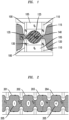
- FIG. 1 is a schematic representation of an interference device for edge currents as seen in plan view.
- One cell is shown; the cell is configured to function, for edge states of a FQHE charge carrier droplet, in a manner analogous to how a Fabry-Perot interferometer operates for light.
- This cell is a basic element that can be replicated and assembled into more complex structures to serve as memory cells and other devices for quantum computing operations.
- the interference device is fabricated on a semiconductor heterostructure, as will be explained in greater detail below.
- the interferometer is defined by pairs of surface gate electrodes 100, 105, 110, which are operated at voltage V b for gates 100 and 110 and at voltage V s for gates 105. At suitable, control values, these voltages deplete the carrier population below them.
- the carriers are electrons. However, the possibility that holes, rather than electrons, constitute the 2DCCG is not excluded.
- the effective area A eff of this droplet is marked in the diagram. More specifically, the area A eff is enclosed by the edge current, i.e., A ff is delimited by the innermost edge current. Because the carrier density within A eff is the bulk density, the confined droplet has, at a given applied magnetic field strength, the same filling factor as the bulk of the fluid outside the interferometer. It should be noted that in operation, the area A eff is smaller than the geometric area A geom defined by the layout of the surface gate electrodes. Between the outer boundary of A eff and the outer boundary of A geom , there is an electron density gradient.
- QH quantum Hall
- the resistance R L provides an observable indication of interference that takes place in the interferometer, and it thus may provide an interferometer output signal.
- the surface gates in operation, create constrictions 135, 140 of the QH fluid droplet.
- Edge current can cross between the upper and lower edges at each of the two constrictions. That is, an edge excitation can tunnel from one edge to the other, as indicated in the figure by the broken lines at constrictions 135 and 140.
- the lateral separation between the gates at the constrictions is indicated in the figure as d g .
- the actual tunneling distance between the edge currents, indicated as d in the figure is controlled by the gate voltage V b .
- an edge current exiting the interferometer cell will contain a contribution that has laterally encircled the region A eff of the interferometer, and also a contribution that has not laterally encircled the region A eff .
- the encircling contribution can acquire a different phase from the non-encircling contribution. This phase difference can cause interference, which is detectable because it modulates the longitudinal resistance R L , which can be measured. For example, resistance oscillations may be observed as the applied magnetic field is swept in value.
- Phase changes may occur due to Aharonov-Bohm phase contribution, and due to statistical phase contribution, both of which are known in the art.
- topological state is a degree of freedom of the QH fluid droplet that is changed by a braiding operation involving quasiparticles for non-Abelian states such as 5/2, 7/2, 12/5 and 17/5. Changes of the topological state can also be manifested by phase accumulation.
- Interference between the encircling and non-encircling paths produces the above-mentioned oscillations in the resistance measured across the interference device.
- the voltages V b on top gates 100, 110 can be adjusted to promote such backscattering, and the voltages V s on top gates 105 can be adjusted to change the enclosed area A eff .
- the distance marked d g in FIG. 1 should be sufficiently large that for nominal voltages V b , the backscattering will be relatively weak, for reasons to be explained below.
- a sufficiently large value for d g will also promote a contiguous extent for 17/5 and 12/5 fractional Hall states, from outside to inside the active area A eff of the interferometer.
- d g it is advantageous for d g to be large enough to permit tuning of the gate voltages to induce stronger and weaker backscattering of quasiparticles, as measured by the non-Abelian Fibonacci anyon braiding oscillations shown in FIG. 8 , which will be discussed below.
- the geometrical gap size affects the range of voltages needed.
- the voltage must lie within the range between the value that is just enough to achieve full depletion directly beneath the gates, and the value at which conduction in the gap is closed off. If the gap is too small, this range may be too narrow to permit a useful amount of tuning.
- the charge of the edge-state carriers is dependent upon the bulk filling factor.
- the "bulk”, as noted above, is the portion of the QH fluid that laterally lies outside the cell and that lies within area A eff . That is, it is the portion that is substantially free of depletion effects.
- the carriers are electrons, and thus they carry the fundamental electronic charge e .
- the bulk filling factor is fractional, the charge on the carriers is determined by the denominator of the fraction that describes the filling factor.
- the bulk filling factor is 1/3, the carriers will be quasiparticles of charge e/3, and if the filling factor is 2/5, the carriers will be quasiparticles of charge e /5.
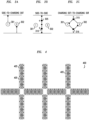
- FIG. 2 is a schematic representation, seen in plan view, of a composite cell that could be useful for qubit operations based on FQHE states.
- the composite cell is constituted as a series of four end-connected interferometer cells 201-204 of the kind described above.
- the constrictions at the boundaries of the cells are labeled, in sequence, with transmission coefficients t 1 -t 5 . These coefficients describe the amount of transmission of edge current, due to backscatter, through the respective constrictions. These values can be individually adjusted by application of suitable voltages to the surface gate electrodes at the two sides of the constrictions.
- Each of the cells shown in FIG. 2 includes a charging dot 205.
- the four charging dots 205 visible in FIG. 2 are respectively numbered from 1 to 4.
- the charging dot is a surface electrode similar to the surface gate electrodes 100-110 of FIG. 1 .
- the charging dots are shown as situated at the centers of their respective cells. Although such a location may be useful for at least some purposes, a central location for the charging dots is not essential.
- a cell may contain more than one charging dot.
- electrical contact to each charging dot or other surface dot may be made via an air bridge.
- Voltages controllably applied to the charging dots are used to manipulate the charge states of the cells. In this manner, operations useful for quantum computation, such as braid operations, can be performed.
- charge manipulations As few as three elementary charge manipulations may provide a sufficient basis for the operations necessary to store topological qubits and to perform quantum computations with them.
- charge manipulations respectively, as side-to-charging-dot, side-to-side, and charging-dot-to-charging-dot operations.
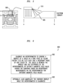
- FIGS. 3A, 3B, and 3C These charge manipulations are respectively illustrated in FIGS. 3A, 3B, and 3C .
- two charging dots called out by reference numerals 301 and 302, are shown.
- a charge is transferred from an edge to a charging dot, or from a charging dot to an edge. As explained above, the charge depends on the pertinent filling factor.
- a charge is transferred from an edge to an opposing edge.
- This process may be abetted by additional electrodes, referred to as "helper dots", such as electrodes 305 and 310.
- helper dots such as electrodes 305 and 310.
- the transfer may, for example, be achieved in multiple steps, such as the three steps that are illustrated by arrows landing on electrode 305, on electrode 310, and on the final side.
- constriction serving as a backscattering port at each end of the cell. It should also be understood that a constriction between two cells can also facilitate charge-transfer operations. Thus, for example, a somewhat more extended constriction may contain helper dots for facilitating a charge transfer from one side of the device to the other.
- helper dots may again be used.
- charge transfer from charging dot 301 to charging dot 302 is shown as proceeding in two steps: A transfer from charging dot 301 to helper dot 315, followed by a transfer from helper dot 315 to charging dot 302.
- a second two-step charge transfer is shown as proceeding, via helper dot 316, in the opposite direction.
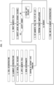
- FIG. 4 is a notional illustration of a possible layout 400 for a topological quantum computer in a schematic plan view. As seen, the layout is built up from cells 405, similar to the cells described above.
- many surface electrodes overlie the same background quantum state of highly correlated electrons (or holes, in other possible implementations), i.e., a 2DCCG. Some of the surface electrodes are used to move charges so as to switch or control the desired quantum states. As will be discussed below, it is desirable for the underlying semiconductor heterostructure to be fabricated with very high purity, so as to provide high-mobility carriers. The higher the purity, the more robust the controllable quantum states will be, and the larger and more stable the output signals will be.
- RIQH integer quantum Hall
- RIQH states can overlie and obscure the Fibonacci states, but the inventor has discovered that under favorable conditions, the presence of RIQH states at filling factors of 17/5 and 12/5 can enhance the interferometer signal from the desired Fibonacci states.
- the inventor believes that there is a density gradient between the bulk portion of the carrier fluid droplet marked as area A eff in FIG. 1 , and the edge of each surface gate electrode. According to the inventor's belief, the density gradient is schematically illustrated graphically in FIG. 5 , for pedagogical purposes.
- a section a-b is indicated. This section extends through the portion of a cell indicated by circle 500, from part of a surface gate electrode, through the depleted region under and near the electrode, and into the bulk portion of the FQHE fluid droplet.
- the right-hand part of the figure is a detail of the indicated portion of the cell, in cross section, shown in a highly simplified manner, which is not to scale.
- the electron density of the 2DCCG directly beneath the electrode edge is very low.
- the electron density increases in gradient region 505, up to the bulk electron density of the 2DCCG in the droplet.
- the local variation in electron density produces an electrical potential gradient, which is schematically illustrated in the figure by electric field lines 510.
- field lines 510 are meant as schematic only; no effort has been made to represent an actual field distribution.
- RIQH phases can form within this density gradient, which is of smaller slope the larger the difference between A eff and A geom .
- the RIQH phases are believed to be formable in immediate proximity to the edge of the bulk region of the FQHE droplet.
- the local reduction in electron surface density near edges of the FQHE droplet is believed to produce, in the re-entrant phases, an electron density corresponding to integer filling factors, e.g., of 3, 2 and/or 1 (for a bulk factor of 17/5) or of integer filling factors of 2 and 1 (for a bulk factor of 12/5).
- the 17/5 and 12/5 states are instances of Fractional quantum Hall states at filling factors greater than 2.
- Interferometric detection of the edge-propagating quasiparticles relies on their coherent transport along the edge of the bulk region having the requisite filling factor. Thus, for detection, edge propagation channels with relatively high edge velocity and thus, relatively low transport times are desirable.
- the interferometer of FIG. 1 is a sub-unit of the structure for storing one qubit.
- the example heterostructure is grown by molecular beam epitaxy (MBE).
- MBE molecular beam epitaxy
- the heterostructure composition in our example implementation is GaAs/AlGaAs.
- the principles described here should not be understood as limited solely to the GaAs/AlGaAs material system, or indeed, to any particular III-V material system, or even as limited solely to III-V material systems.
- a possible alternative to the primary quantum well layer of GaAs described below is a primary well layer of InGaAs.
- the heterostructure is advantageously operated with an electron density in the 2D electron gas that is, substantially, at least 4 ⁇ 10 11 cm -2 .
- the term "substantially”, here and throughout this document, means “within plus or minus ten percent”.
- the target electron density can be achieved through conventional processes of doping adjustment known in the field of MBE growth, including the known use of shielding wells above and below the principal well where the 2DCCG resides.
- the MBE growth tool includes a source of aluminum for the epitaxial growth of AlGaAs.
- a source of aluminum of high purity may be produced by purifying the aluminum source, prior to growth, by known methods.
- a suitable method of aluminum purification is published, for example, at Y.J. Chung et al., "Surface segregation and the Al problem in GaAs quantum wells," Phys. Rev. Materials 2, 034006 (2018 ).
- An interferometric device fabricated using an aluminum source produced using this purification method is described at R.L. Willett et al., "Interference measurements of non-Abelian e/4 & Abelian e/2 quasiparticle braiding," arXiv:1905.10248 (2019 ).
- the interferometer constitutes a basic element of an FQHE qubit storage and computation hardware.
- the interferometer includes a set of surface gates formed on the heterostructure. Upon application of negative bias, the surface gates deplete the, e.g., electrons that lie directly beneath them and that lie below and in lateral proximity to them.
- the geometrical conformation of the surface gates creates a cell of geometric area A geom , as described above with reference to FIGS. 1-4 , for example, with a port for entry and egress at each of its two ends. Similar cells are known in the art, and it is likewise known that several cells can be joined together to form a qubit storage and manipulation hardware, as in FIG. 4 , for example.
- the interferometer devices have large enclosed active areas, large lateral gaps at the backscattering ports, and one or more central top gate dots in the active area.
- the geometric area A geom of the interferometer is defined, in an example, by the dimension from the upper to the lower side (i.e., V s ) electrodes, and from the lateral distance between the backscatter (V b ) electrodes.
- the side dimension of A geom is preferably at least 2 ⁇ m.
- the large area is typically desired so that a large lateral dimension can be accommodated between the energized surface gate and the interior bulk electron density, i.e., the bulk electron density within area A eff .
- the re-entrant phases of integer quantum Hall states can form within the density gradient between the interior bulk density and the edge of the surface gate.
- the re-entrant phase(s) may form in proximity to the edge of the interior bulk region of area A eff As explained above, the electric potential gradient due to the re-entrant phases is believed to have the beneficial effects of enhancing edge-current velocity and thus, shielding against decoherence of the FQHE carrier droplet.
- Each of the entry ports has a gap width d g between the surface gates at the constrictions where the entry ports are located.
- These gaps in the entry ports are preferably large, like the relatively enlarged area A geom , to better accommodate the re-entrant phases.
- a central charging dot electrode was used in prototype devices, but one or more dot electrodes centrally or non-centrally located can be used. Multiple charging dots may be useful, for example, to implement charge-transfer patterns for qubit operations such as those described above. It should be noted in this regard that not all charging dots or helper dots are necessarily charged in operation. For example, there may be operating modes in which one or more dots are maintained at ground potential.
- US Patent 8987703 discusses advantageous lattice orientations for FQHE droplet devices.
- US Patent 8362461 discusses quantum well structures for FQHE droplet devices that contain screening wells that may be advantageous for screening impurity ions.
- US Patent Application Publication 2023/240155 A1 describes a transparent surface gate that may be advantageous for use in FQHE droplet devices, potentially including the devices described here.
- the process of activating the device typically includes illuminating the device with light prior to applying gate voltages, and tuning the gate voltages at the backscattering ports to producing re-entrant QHE state phases, e.g., one or more integer QHE phase regions along an edge or edges of the FQHE droplet, so that the transport of one or more edge excitations of the FQHE droplet may be enhanced.
- re-entrant QHE state phases e.g., one or more integer QHE phase regions along an edge or edges of the FQHE droplet, so that the transport of one or more edge excitations of the FQHE droplet may be enhanced.
- All gate electrodes are held at ground potential during illumination, which is believed to activate the carriers from impurity sites to the 2DCCG.
- a useful illumination process is described, for example, in the paper by R.L. Willett et al. that was cited above.
- the illumination step seems to help to achieve a saturation carrier density of the 2DCCG for operation. When this density is reached, the illumination is terminated.
- Another effect of the illumination step is to produce uniformity in the distribution of carrier density, which can assist excitation propagation on the edges of the FQHE carrier droplet.
- Re-entrant states have a characteristic "re-entrance" property that can be observed in the interferometer during a sweep of the applied magnetic field. This property is seen as quantization in the Hall resistance at a transverse resistance of (1/3)h/e 2 near a filling factor of 17/5, and at a resistance of (1/2) h / e 2 near a filling factor of 12/5.
- h Planck's constant
- e is the absolute value of the elementary electronic charge.
- FIG. 6 is a flowchart illustrating a general method 600 for operating various apparatus described herein.
- the apparatus includes a set of interferometers located along a surface of a substrate having a quantum well therein, and each interferometer has a cell and a set of gate electrodes located around the cell.
- the quantum well is operable to trap a 2D charge carrier gas (2DCCG) such that the trapped 2DCCG extends along the surface.
- some specific examples of the substrate are group III-V semiconductor heterostructure substrates including a primary quantum well having a GaAs well layer between AlGaAs barrier layers, wherein each AlGaAs barrier layer includes a shielding quantum well.
- Such heterostructures may include one or more silicon dopant layers located such that one of the shielding quantum wells is between each silicon dopant layer and the primary GaAs well layer. Nevertheless, the inventor does not intend that the substrate be limited to such examples of group III-V heterostructures. Indeed, other types of substrates with a quantum well for trapping a 2DCCG, e.g., other semiconductor substrate structures, may be usable in embodiments of methods and structures as described herein.
- the method 600 involves calibrating one or more of the interferometers of the set to confine a droplet of the 2DCCG in a fractional quantum Hall effect (FQHE) state of filling factor 17/5 or 12/5 in an area of the cell thereof.
- the calibrating is performed such that a reentrant phase of integer quantum Hall effect (IQHE) states of the 2DCCG is located between the area of the droplet of the 2DCG in a FQHE state and the electrodes of the same interferometer.
- the calibrating step includes setting a value of a magnetic field across the substrate such that the reentrant phase and the droplet of the 2DCCG are present in such interferometer(s) based on interference measurements on the same interferometer(s) for different values of the magnetic field.
- the calibrating may also use the interference measurements to determine whether a reentrant phase of IQHE states of the 2DCCG is present in the same interferometer(s).
- the method 600 may optionally include measuring and/or varying a topological property of the droplet of the 2DCCG confined in one or more of the interferometers while maintaining the calibration of the same interferometer(s).
- the method 600 may optionally further include, e.g., manipulating the 2DCCG while maintaining the calibration of the same interferometers to read and/or store a qubit value stored in a selected one of the calibrated interferometers, and/or to braid qubit states confined to two or more selected ones of the calibrated interferometers.
- the method 600 may further include illuminating the substrate to increase a density of the charge carriers in the 2DCCG, stopping the illuminating, and then, applying voltages to the gate electrodes of the interferometers to form the droplets in the interferometers.
- FIG. 7 is a flowchart illustrating specific examples of the processes of FIG. 6 . It should be borne in mind that FIG. 7 is illustrative only, and should not be understood as limiting as to the precise natures of the various operations or the order in which they are performed.
- Blocks A and B of FIG. 7 may correspond to activation block 601 of FIG. 6 .
- the heterostructure is cooled.
- it is illuminated. It should be understood that although illumination has proven to be an effective approach for activating the device, it is not considered to be critical.
- a red LED provided the illumination.
- the illumination is one useful approach for increasing the carrier mobility and the carrier (e.g., electron) density in the quantum well.
- carrier e.g., electron
- bulk carrier density for operation may lie substantially within the range 4 ⁇ 10 11 to 6 ⁇ 10 11 electrons per square centimeter.
- Blocks C-K of FIG. 7 may correspond to calibration block 602 of FIG. 6 .
- the initial gate voltages are set.
- the voltages V b applied to the backscattering gates and the voltages V s applied to the side gates are typically sufficient to fully deplete the electrons of the 2DCCG in the quantum well immediately below the surface gates.
- One effect of this is to reduce the active region of the cell, i.e., the region having the bulk carrier density, to an area A eff that is smaller than the geometric area A geom of the cell.
- a neck of the carrier gas also extends through the constrictions at the ends of the cell.
- the gate voltages will generally be tuned to produce larger or smaller amounts of confinement at the constrictions, or to affect interference signal strength in other ways. Example voltages are provided elsewhere in this discussion.
- the voltage-tuning range is limited by the geometric dimensions A geom and d g , because, for the interferometer to operate as intended, there must be a contiguous body of the 2D charge carrier gas at bulk density that can support the re-entrant phase(s) and 17/5 and 12/5 states. This contiguous body must extend through the cell, including through the constrictions at its ends. If the applied voltages are too great, the depleted region will encroach too far, and will cut off the contiguity of the bulk region within the cell. Hence, it is desirable for the cell to be fabricated with dimensions in A geom and d g that are large enough to support a useful voltage-tuning range.
- the external magnetic field is applied.
- this field will be swept through integer filling factors to determine the fundamental interference oscillation period due to an electron encircling an additional single magnetic flux quantum in the device.
- the period exposed by the interferometer at integer filling, where electrons are encircling the continuous addition of magnetic flux quanta as the field is swept, is the magnetic field period F 0 of the interference oscillation.
- the quantity F 0 is an important calibration factor, because it is the metric for knowing the periods at filling factors of 12/5 and 17/5 that represent non-Abelian interference.
- the magnetic field will then be swept through filling factors 17/5 and 12/5 and through their surrounding re-entrant filling factors.
- the presence and the quality of these states are assessed through transport measurements that are made with the surface gate voltages nominally achieving depletion beneath the gates.
- Interferometry is initiated. Interferometry can be performed by holding the gate voltages fixed and sweeping the magnetic field, by holding the magnetic field fixed and varying the gate voltages, or by a combination of both approaches.
- the gate voltages are constant and the magnetic field is swept.
- At least one central top gate can be part of the device operation.
- a gate can, e.g., hold single quasiparticle charges.
- such gates can be used to transfer single quasiparticles, or can be used passively as a grounded surface layer.
- the interferometric signal is obtained by measuring resistance across the cell in the longitudinal and in the transverse direction.
- the transverse resistance is a Hall resistance.
- the interference oscillations are observed within these signals.
- the F 0 value should be reassessed, to maintain accurate calibration for the periods of the target interference at 17/5 and 12/5.
- the external magnetic field strength is swept, e.g., in an interval about the filling factor of 17/5 or 12/5, and changes in electrical resistance across one or more cells are observed.
- the resulting trace may exhibit oscillations of various kinds, including: Aharonov-Bohm oscillations, statistical phase oscillations (particularly for surrounding Abelian correlated states), and oscillations due to quasiparticle number change in the non-Abelian candidate states 12/5 and 17/5. The latter are confirmed if their experimental periods, as determined by calculations involving the host filling factor and the pre-measured simple electron interference F 0 , correspond to their prescribed values.
- the calibration procedure can be terminated, although it may be repeated later, for example if the gate voltages are changed.
- the gate voltages can be re-tuned as indicated at block I, and a new sweep can be performed.
- the magnetic field can be extracted and the gates turned off, and a re-illumination cycle can be performed, as indicated at block J.
- the magnetic field strength can be calibrated to produce the desired 17/5 or 12/5 FQHE state.
- the magnetic field strength can be calibrated to produce the desired 17/5 or 12/5 state.
- Blocks L and M of FIG. 7 may correspond to the optional manipulation block 603 of FIG. 6 on the calibrated apparatus.
- Quantum computation can then be carried out through braiding operations in the respective cells.
- the braiding operations are able to switch the topological states of the cells. These changed states are manifested as changes in the phase of the interference pattern that is read out as a resistance signal.
- a braid is performed by localizing each component of a pair of anyons and causing current to pass between the localized anyons.
- Current in this regard, may be controllable at a level of granularity as small as a single charge.
- the topological state is set by the braiding history of the component quasiparticles.
- Suitable charge manipulations for the braiding operations are described elsewhere in this discussion.
- the above-described process in which centrally located charging- dot electrodes, populated with e / 5 charges, aid in moving a quasiparticle of charge e / 5 from one side of a cell to the other side can be a fundamental topological state switch.
- the topological states of the cells can be measured from the edge-current interference, before and after the manipulations.
- doping was from delta doped silicon layers on both sides of the quantum well, with a narrow intermediate shielding well of GaAs, less than 2 nm thick, between the dopant layers and the principal quantum well, which had a nominal width of 20 nm.
- the silicon doping was contained within a narrow GaAs well, 1 nm thick, removed from and on either side of the principal quantum well.
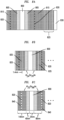
- FIGS. 8A to 8C A basic design and these two variations are illustrated in FIGS. 8A to 8C , which are discussed in detail below.
- the samples that we prepared ranged in density from 3 ⁇ 10 11 to 4.5 ⁇ 10 11 electrons/cm 2 . Highly purified Al was used in the sample preparation for the heterostructures with intermediate GaAs shielding wells.
- Interferometer design Contacts formed from Ni/Au/Ge/Ni layering were diffused into the perimeter of a mesa for containing the 2DCCG, and the areas between the contacts were left for deposition of the top gate structures that form the interferometers. After contact formation and diffusion, a 30-nm layer of amorphous SiN was deposited on the mesa to further insulate the 2DCCG from the top gate structures.
- the top gates were formed from Al and Au layers, Ti and Au and Al layers, or from Ti and Au layers. The top gate layers did not exceed 120 nm in thickness. The samples were illuminated to activate carriers after mounting and cooling in a dilution refrigerator, but prior to charging the top gates.
- the temperature at which illumination was applied ranged from room temperature to the base temperature of 20 mK, and varied dependent upon the doping structure of the heterostructure to optimize transport quality. Illumination helps achieve maximum potential mobilities, and seems to enable achieving a higher anyon state energy gap.
- the top gates were charged to a negative voltage sufficient to deplete the underlying lateral portion of the 2D electron gas layer.
- the active area A eff is , in operation, the area enclosed by the edge currents in the quantized Hall systems and is often not the full lateral area between the electrodes of the cell. Rather, the area A eff is electrostatically determined by the applied gate voltages.
- the lateral area between the electrodes of a cell in all of the prototypes that we tested was several square micrometers, but the active area A eff was typically less than one square micrometer. In example prototype devices that we fabricated, the full lateral area between the electrodes of a cell was roughly 9 ⁇ m 2 .
- Each charging dot electrode was electrically accessed by an air bridge that extended over one of the side gates, such as those marked V s in FIG. 1 .
- Resistance and resistance oscillations were measured using low noise lock-in amplifier techniques.
- a constant current typically 2 nA was driven through the 2D electron system as laterally defined by the surface interferometer gate structure, and the voltage, and so resistance, was determined with a four- terminal measurement.
- Heterostructure designs Our basic heterostructure design, which we refer to as the normal well design, will be described first.
- the heterostructures were grown by MBE on GaAs wafers.
- the backscatter-port-to-backscatter-port direction of each cell was aligned along the crystallographic [110] direction of the substrate. If the port-to-port direction were instead aligned orthogonal to this direction, large backscattering might occur away from the backscattering ports, possibly degrading performance of the cell.
- the shielded well design has a small addition to the fundamental well design. Between each doping layer and the quantum well, but within the 32% Al fraction layer, are placed thin wells 835 of GaAs, about 1nm in thickness. These layers, on either side of the 2D system in the central 24-nm quantum well, accept a low density of electrons, and they demonstrate some parallel conduction in magneto-transport measurements, confined to low magnetic fields.
- the shield layers appear to provide a smoothing effect on the potentials presented by the ionized doping layers, resulting in stronger electron correlations in the central well. This may produce a high mobility and thus, larger correlated state gaps.
- the shield layers can shield the central well itself.
- the doping well design is distinguished in that the Si dopants are placed in narrow GaAs wells within the high Al concentration layers.
- This design has demonstrated high mobilities and large fractional quantum Hall state gaps.
- the surface gates do not modulate the underlying 2D electron system density in a usable way at operational temperatures.
- the only method by which these structures can be used for interferometry is to set the gates at working voltages at higher temperatures, for example at about 4K, and to operate at base temperatures performing only magnetic field sweeps.
- Performance optimization can be achieved empirically.
- the parameter set for optimization includes doping levels, shielded well and doping well widths, widths of intermediate layers of high Al concentration, central well widths, temperatures for deposition at each of these stages, and cap layer thicknesses.
- Sample illumination and gating processe s. Illumination may be accomplished by exciting a red LED positioned over the sample. Illumination has been performed, e.g., at a temperature below the 2D electron Fermi energy, which is about 100K.
- the optimal duration of illumination and the optimal temperature or temperatures at which the light is applied are specific to the devices under preparation, and may be determined by empirical experimentation. By way of example, we successfully prepared doping well samples with continuous illumination during cool-down from room temperature to 4K, at which point the illumination was stopped.
- the gates are energized after illumination, with the LED light source turned off.
- the gates could be successfully charged at 4K.
- the active cell area is the area bounded by an edge current whose charge corresponds to the bulk filling factor. It should be noted, however, that a series of edge currents will populate the space from the innermost edge where the bulk edge current is located, out to the fully depleted edge. These currents will correspond to the states between the bulk filling factor and zero filling factor. For proper operation of the interferometer, reflection should primarily be only of the innermost edge currents.
- the width of the gate is the path length over which the edge currents are brought into proximity.
- the gate width and the separation d g define the potential tunneling paths for the edge currents, and they determine the transparency of the constrictions.
- An effective gate width may be determined empirically.
- the voltage applied to the backscattering gates typically depletes the underlying 2D electrons.
- the separation between the gate electrodes accommodates this condition.
- a large separation d g can be compensated by a large range in applied gate voltages. Typical values for d g are about 1 ⁇ m, with an applied voltage of 4V.
- FIG. 9 is an electron microscopic image of a portion of a prototype device.
- the backscattering gates 900 and the side gates 905 are visible in the image.
- a geometrical separation, i.e., a separation as defined for fabrication, of 3 ⁇ m between the side gates is indicated in the figure.
- the two large pads 910 seen in figure are landing pads for airbridges, which could connect to dot electrodes overlying the active area.
- the surface gates shown in the figure are not used to inject charge into, or extract charge from, the 2D carrier gas. Accordingly, they are not diffused into the heterostructure to make contact with it, but rather, they are used for carrier depletion.
- the metal contacts which are not visible in FIG. 9 , are layered stacks of different metals. They were deposited in specific locations away from the surface gates, and thermally diffused through the top heterostructure layers to the quantum well. The surface gates were patterned and deposited after the contact diffusion.
- FIG. 10 is a graph of experimental measurements performed on a prototype device of the shielded well design, substantially as described above.
- electrical resistance in kilo-Ohms
- the vertical axis ranges from 0 k ⁇ to 1.2 k ⁇ . Signatures of various excitations are seen as peaks and valleys in the main part of the figure.
- the integer filling factors within range of the magnetic field scan are 4, 3, and 2. Their positions in the scan are indicated on the graph in the main part of the figure. Certain fractional filling factors, which correspond to features in the graph, are also indicated. They are the factors of 7/2, 17/5, 8/3, 5/2, 12/5, and 7/3. Signatures of the re-entrant phases near 7/2 and 5/2 are expressly called out. In addition, the signatures of the Fibonacci anyon states at 17/5 and 12/5 are expressly called out, and are shown in magnified view in respective insets to the figure.
- FIG. 11 is a magnified view of the inset of FIG. 10 for the 17/5 state. As seen in the figure, Fibonacci anyon oscillations are present, and are distributed around the magnetic field value corresponding to the 17/5 filling factor.
- F 0 is the period to add one flux quantum
- a ff ⁇ 0 /F 0 .
- FIG. 12 is a magnified view of the inset of FIG. 10 for the 12/5 state.
- Fibonacci anyon oscillations are present, and are distributed around the magnetic field value corresponding to the 12/5 filling factor. These oscillations also have the predicted period for additions of roughly three quasiparticles of charge e/5 as the magnetic field is swept.
Landscapes
- Engineering & Computer Science (AREA)
- General Physics & Mathematics (AREA)
- Theoretical Computer Science (AREA)
- Physics & Mathematics (AREA)
- Mathematical Analysis (AREA)
- Computing Systems (AREA)
- Evolutionary Computation (AREA)
- Condensed Matter Physics & Semiconductors (AREA)
- Computational Mathematics (AREA)
- Mathematical Optimization (AREA)
- Pure & Applied Mathematics (AREA)
- Data Mining & Analysis (AREA)
- General Engineering & Computer Science (AREA)
- Mathematical Physics (AREA)
- Software Systems (AREA)
- Artificial Intelligence (AREA)
- Computer Hardware Design (AREA)
- Junction Field-Effect Transistors (AREA)
- Hall/Mr Elements (AREA)
Claims (14)
- Verfahren (600) zum Betreiben einer Einrichtung, die einen Satz von Interferometern (201-204) beinhaltet, die entlang einer Fläche eines Substrats angeordnet sind, wobei das Substrat einen Quantentopf aufweist, der betreibbar ist, ein 2D-Ladungsträgergas einzufangen, derart, dass sich das eingefangene 2D-Ladungsträgergas entlang der Fläche erstreckt, wobei jedes Interferometer eine Zelle und einen Satz von Gateelektroden, die um die Zelle herum angeordnet sind, aufweist, wobei das Verfahren Folgendes umfasst:Kalibrieren (602) von jedem der Interferometer, um ein Tröpfchen des 2D-Ladungsträgergases (125) in einem fraktionierten Quantenhalleffektzustand eines Füllfaktors 17/5 oder 12/5 in einem Bereich der Zelle davon zu begrenzen, während eine ablaufinvariante Phase von ganzzahligen Quantenhalleffektzuständen des 2D-Ladungsträgergases zwischen dem Bereich des Tröpfchens des 2D-Ladungsträgergases in einem fraktionierten Quantenhalleffektzustand und den Elektroden (100, 105, 110) des einen der Interferometer angeordnet ist;wobei das Kalibrieren das Einstellen eines Wertes eines Magnetfeldes über das Substrat beinhaltet, derart, dass auf Basis von Interferenzmessungen an dem mindestens einen der Interferometer auf verschiedene Werte des Magnetfeldes die ablaufinvariante Phase und das Tröpfchen des 2D-Ladungsträgergases in mindestens einem der Interferometer vorhanden sind; undwobei das Kalibrieren das Verwenden der Interferenzmessungen umfasst, um zu bestimmen, ob eine ablaufinvariante Phase von ganzzahligen Quantenhalleffektzuständen des 2D-Ladungsträgergases in dem mindestens einen der Interferometer vorhanden ist.
- Verfahren nach Anspruch 1, das ferner Folgendes umfasst (603) :
Messen oder Variieren einer topologischen Eigenschaft des Tröpfchens des 2D-Ladungsträgergases, das auf ein oder mehrere der Interferometer des Satzes begrenzt ist, während die Kalibrierung der Interferometer beibehalten wird. - Verfahren nach Anspruch 1 oder 2, das ferner Folgendes umfasst:
Manipulieren des 2D-Ladungsträgergases, während die Kalibrierung der Interferometer beibehalten wird, um mindestens eines von Folgendem durchzuführen:Lesen eines Qubitwertes, der in einem ausgewählten der kalibrierten Interferometer gespeichert ist,Speichern eines Qubitwertes im ausgewählten der kalibrierten Interferometer, undDurchführen einer Flechtoperation von Qubitzuständen, die auf zwei oder mehr ausgewählte der kalibrierten Interferometer begrenzt sind. - Verfahren nach einem der Ansprüche 1 bis 3, wobei das Substrat eine Gruppe-III-V-Halbleiterheterostruktur beinhaltet, die Folgendes umfasst:einen primären Quantentopf, der eine InGaAs- oder eine GaAs-Topfschicht (800) zwischen AlGaAs-Sperrschichten (805) aufweist, wobei jede AlGaAS-Sperrschicht einen abschirmenden Quantentopf (835) beinhaltet; undmindestens eine Siliziumdotandschicht (820), die derart angeordnet ist, dass sich einer der abschirmenden Quantentöpfe zwischen der Siliziumdotandschicht und der InGaAs- oder der GaAs-Topfschicht befindet.
- Verfahren nach einem der Ansprüche 1 bis 4, das ferner Folgendes umfasst:
Beleuchten des Substrats, um eine Dichte der Ladungsträger im 2D-Ladungsträgergas zu erhöhen, Stoppen des Beleuchtens und dann Anlegen von Spannungen an die Gateelektroden, um die Tröpfchen in den Interferometern zu bilden. - Verfahren nach Anspruch 5, wobei das Kalibrieren in Reaktion auf das Bestimmen, dass eine ablaufinvariante Phase in dem mindestens einen der Interferometer nicht vorhanden ist, ferner Folgendes umfasst:erneutes Beleuchten des Substrats; undnach Stoppen des erneuten Beleuchtens Verwenden von Interferenzmessungen, um zu bestimmen, ob eine ablaufinvariante Phase von ganzzahligen Quantenhalleffektzuständen des 2D-Ladungsträgergases in dem mindestens einen der Interferometer vorhanden ist.
- Verfahren nach Anspruch 6, wobei die Kalibrierung während des Variierens des Magnetfeldes das Messen von Oszillationen in den Interferenzmessungen aufgrund von einigem oder allem von Folgendem umfasst: Aharonov-Bohm-Oszillationen, statistischen Phasenoszillationen und Oszillationen aufgrund einer Quasiteilchenanzahländerung eines nichtabelschen Zustands für den Füllfaktor 12/5 oder den Füllfaktor 17/5.
- Verfahren nach Anspruch 7, wobei in einem Fall, in dem Oszillationen eines aus dem Satz, der aus Aharonov-Bohm-Oszillationen, statistischen Phasenoszillationen und Oszillationen aufgrund einer Quasiteilchenanzahländerung in nichtabelschen Zuständen, die mit dem Füllfaktor 12/5 oder dem Füllfaktor 17/5 verknüpft sind, ausgewählten Typs nicht beobachtet werden konnten, die Kalibrierung ferner Folgendes umfasst:erneutes Beleuchten des Substrats; undnach Stoppen des erneuten Beleuchtens Wiederholen des Variierens des Magnetfeldes und während des Variierens des Magnetfeldes Messen von Oszillationen in den Interferenzmessungen aufgrund von einigem oder allem von Folgendem: Aharonov-Bohm-Oszillationen, statistischen Phasenoszillationen und Oszillationen aufgrund einer Quasiteilchenanzahländerung eines nichtabelschen Zustands für den Füllfaktor 12/5 oder den Füllfaktor 17/5.
- Verfahren nach einem der Ansprüche 5 bis 8, wobei die Ladungsträger des 2D-Ladungsträgergases Elektronen sind und das Beleuchten bewirkt, dass eine Raumdichte der Elektronen im 2D-Ladungsträgergas im Wesentlichen größer ist als 4 x 10¹¹ pro Quadratzentimeter der Fläche.
- Verfahren nach Anspruch 1, wobei jedes der Interferometer einen Satz von Seitenelektroden (105) und einen Satz von Rückstreuelektroden (100, 110) beinhaltet und das Verfahren ferner Folgendes umfasst:Anlegen von Spannungen (VS) an die Seitenelektroden eines spezifischen der Interferometer, um einen Bereich um die Zelle des spezifischen der Interferometer des 2D-Ladungsträgergases zu entleeren; undAnpassen von Spannungen (Vb), die über die Rückstreuelektroden des spezifischen der Interferometer angelegt sind, um ein Rückstreuen von Kantenerregungen des Tröpfchens im spezifischen der Interferometer zu ändern.
- Verfahren nach Anspruch 10, wobei ein Muster, das eine oder mehrere Punktelektroden (205, 301, 302, 305, 310, 315, 316) umfasst, die Zelle des spezifischen der Interferometer überlagert, wobei die eine oder die mehreren Punktelektroden von den Seiten- und den Rückstreuelektroden des spezifischen der Interferometer elektrisch isoliert sind; und
das Verfahren umfasst ferner das Anlegen einer Spannung an eine ausgewählte der Punktelektroden des Punktmusters derart, dass eine Ladung im 2D-Ladungsträgergas in der Nähe der ausgewählten Punktelektrode angeordnet wird. - Verfahren nach Anspruch 11, das ferner Folgendes umfasst:
Variieren einer Spannung, die an die ausgewählte Punktelektrode angelegt ist, derart, dass eine Ladung im 2D-Ladungsträgergas in der Nähe einer anderen der einen oder der mehreren Punktelektroden angeordnet wird. - Verfahren nach Anspruch 11, das ferner Folgendes umfasst:
Variieren einer Spannung, die an die ausgewählte Punktelektrode angelegt ist, derart, dass sich eine Ladung zwischen benachbarten gegenüberliegenden Rückstreuelektrode bewegt. - Verfahren nach Anspruch 11, das ferner Folgendes umfasst:
Variieren einer Spannung, die an die ausgewählte Punktelektrode angelegt ist, derart, dass eine Ladung von einer lokalisierten Position an der ausgewählten Punktelektrode zu einer der Seitenelektroden oder einer der Rückstreuelektroden des spezifischen der Interferometer verschoben wird.
Applications Claiming Priority (1)
| Application Number | Priority Date | Filing Date | Title |
|---|---|---|---|
| US202263353842P | 2022-06-21 | 2022-06-21 |
Publications (2)
| Publication Number | Publication Date |
|---|---|
| EP4297553A1 EP4297553A1 (de) | 2023-12-27 |
| EP4297553B1 true EP4297553B1 (de) | 2025-03-26 |
Family
ID=83192111
Family Applications (1)
| Application Number | Title | Priority Date | Filing Date |
|---|---|---|---|
| EP22193613.1A Active EP4297553B1 (de) | 2022-06-21 | 2022-09-02 | Verfahren zum zugriff auf fibonacci-anyone zur topologischen quantenberechnung in einem korrelierten zweidimensionalen elektronensystem |
Country Status (2)
| Country | Link |
|---|---|
| US (1) | US12446280B2 (de) |
| EP (1) | EP4297553B1 (de) |
Families Citing this family (1)
| Publication number | Priority date | Publication date | Assignee | Title |
|---|---|---|---|---|
| WO2025248692A1 (ja) * | 2024-05-30 | 2025-12-04 | 株式会社日立製作所 | 量子デバイス及び量子情報処理装置 |
Family Cites Families (11)
| Publication number | Priority date | Publication date | Assignee | Title |
|---|---|---|---|---|
| CN1839093B (zh) | 2003-08-20 | 2011-02-09 | 库克有限公司 | 纳米级或原子级器件及其制造方法 |
| US7250624B1 (en) * | 2005-09-23 | 2007-07-31 | Microsoft Corporation | Quasi-particle interferometry for logical gates |
| US20070194225A1 (en) | 2005-10-07 | 2007-08-23 | Zorn Miguel D | Coherent electron junction scanning probe interference microscope, nanomanipulator and spectrometer with assembler and DNA sequencing applications |
| US8209279B2 (en) | 2007-09-07 | 2012-06-26 | Microsoft Corporation | Measurement-only topological quantum computation |
| US8362461B2 (en) | 2008-12-12 | 2013-01-29 | Alcatel Lucent | Quantum well device |
| US7960714B2 (en) | 2008-12-12 | 2011-06-14 | Alcatel-Lucent Usa Inc. | Interfering excitations in FQHE fluids |
| US8987703B2 (en) * | 2011-12-02 | 2015-03-24 | Alcatel Lucent | Quantum well device with lateral electrodes |
| US9721209B2 (en) | 2013-10-14 | 2017-08-01 | Microsoft Technology Licensing, Llc | Method and system for efficient decomposition of single-qubit quantum gates into Fibonacci anyon braid circuits |
| CN106575667B (zh) | 2014-07-02 | 2020-07-31 | 哥本哈根大学 | 半导体约瑟夫森结及其相关的传输子量子位 |
| US11342017B2 (en) | 2018-10-26 | 2022-05-24 | Nokia Technologies Oy | Key-based multi-qubit memory |
| JP7250922B2 (ja) | 2018-10-26 | 2023-04-03 | ノキア テクノロジーズ オサケユイチア | 量子計算装置のためのメモリセルの配置 |
-
2022
- 2022-09-02 EP EP22193613.1A patent/EP4297553B1/de active Active
-
2023
- 2023-06-20 US US18/337,949 patent/US12446280B2/en active Active
Also Published As
| Publication number | Publication date |
|---|---|
| EP4297553A1 (de) | 2023-12-27 |
| US20250151351A1 (en) | 2025-05-08 |
| US12446280B2 (en) | 2025-10-14 |
Similar Documents
| Publication | Publication Date | Title |
|---|---|---|
| Waugh et al. | Measuring interactions between tunnel-coupled quantum dots | |
| US6597010B2 (en) | Solid-state quantum dot devices and quantum computing using nanostructured logic gates | |
| Camino et al. | Quantum transport in electron Fabry-Perot interferometers | |
| EP1788637A1 (de) | Infrarotdetektor | |
| EP2786410B1 (de) | Quantenschachtvorrichtung mit seitlichen elektroden | |
| CN114823880B (zh) | 半导体量子点器件及制备方法、信号读取方法和操控方法 | |
| US12446280B2 (en) | Method to access fibonacci anyons for topologicial quantum computation in a correlated two-dimensional electron system | |
| Massai et al. | Impact of interface traps on charge noise, mobility and percolation density in Ge/SiGe heterostructures | |
| Sahu et al. | Ground-state phase diagram and parity-flipping microwave transitions in a gate-tunable Josephson junction | |
| Fuhrer et al. | Transport properties of quantum dots with steep walls | |
| Descamps et al. | Semiconductor membranes for electrostatic exciton trapping in optically addressable quantum transport devices | |
| EP4292137B1 (de) | Begrenzung von neutralen exzitonen in einer halbleiterschichtstruktur | |
| Boselli et al. | Electronic transport in submicrometric channels at the LaAlO 3/SrTiO 3 interface | |
| Ismail | The study of electron transport in field-effect-induced quantum wells on GaAs/GaAlAs | |
| Thureja et al. | Tunable quantum confinement of neutral excitons using electric fields and exciton-charge interactions | |
| Alava | Epitaxial aluminium gates in ultra-shallow GaAs/AlxGa1-xAs heterostructures for low disorder nanoelectronics | |
| Mittag | Electronic Transport in InAs Quantum Devices | |
| Ensslin | Semiconductor quantum devices: from GaAs to graphene | |
| Yang et al. | Fabrication and characterization of GaAs/AlGaAs lateral quantum dot developed by ultrasonic agitation | |
| Su | Andreev bound states in superconductor-quantum dot chains | |
| Noorhidayati | Resistively-detected Nuclear Magnetic Resonance in a Confined GaAs/AlGaAs Structure | |
| Heremans | Transverse magnetic focusing in two-dimensional systems at gallium arsenide/aluminum gallium arsenide heterojunctions | |
| Wagner et al. | G-factor, effective mass and spin susceptibility of a 2-dimensional electron gas | |
| Storace | Magneto-electrical transport through MBE-grown III-V semiconductor nanostructures: from zero-to one-dimensional type of transport | |
| Zhang et al. | Ground-state transition in few-electron quantum dots observed by magnetophotoluminescence |
Legal Events
| Date | Code | Title | Description |
|---|---|---|---|
| PUAI | Public reference made under article 153(3) epc to a published international application that has entered the european phase |
Free format text: ORIGINAL CODE: 0009012 |
|
| STAA | Information on the status of an ep patent application or granted ep patent |
Free format text: STATUS: THE APPLICATION HAS BEEN PUBLISHED |
|
| AK | Designated contracting states |
Kind code of ref document: A1 Designated state(s): AL AT BE BG CH CY CZ DE DK EE ES FI FR GB GR HR HU IE IS IT LI LT LU LV MC MK MT NL NO PL PT RO RS SE SI SK SM TR |
|
| STAA | Information on the status of an ep patent application or granted ep patent |
Free format text: STATUS: REQUEST FOR EXAMINATION WAS MADE |
|
| 17P | Request for examination filed |
Effective date: 20240627 |
|
| RBV | Designated contracting states (corrected) |
Designated state(s): AL AT BE BG CH CY CZ DE DK EE ES FI FR GB GR HR HU IE IS IT LI LT LU LV MC MK MT NL NO PL PT RO RS SE SI SK SM TR |
|
| GRAP | Despatch of communication of intention to grant a patent |
Free format text: ORIGINAL CODE: EPIDOSNIGR1 |
|
| RIC1 | Information provided on ipc code assigned before grant |
Ipc: B82Y 10/00 20110101ALN20241107BHEP Ipc: H01L 29/76 20060101ALI20241107BHEP Ipc: H01L 29/423 20060101ALI20241107BHEP Ipc: H01L 29/12 20060101ALI20241107BHEP Ipc: H01L 29/66 20060101ALI20241107BHEP Ipc: G06N 10/40 20220101ALI20241107BHEP Ipc: G06N 10/20 20220101ALI20241107BHEP Ipc: G11C 11/18 20060101ALI20241107BHEP Ipc: H10N 59/00 20230101ALI20241107BHEP Ipc: H10N 52/00 20230101AFI20241107BHEP |
|
| STAA | Information on the status of an ep patent application or granted ep patent |
Free format text: STATUS: GRANT OF PATENT IS INTENDED |
|
| RIC1 | Information provided on ipc code assigned before grant |
Ipc: B82Y 10/00 20110101ALN20241113BHEP Ipc: H01L 29/76 20060101ALI20241113BHEP Ipc: H01L 29/423 20060101ALI20241113BHEP Ipc: H01L 29/12 20060101ALI20241113BHEP Ipc: H01L 29/66 20060101ALI20241113BHEP Ipc: G06N 10/40 20220101ALI20241113BHEP Ipc: G06N 10/20 20220101ALI20241113BHEP Ipc: G11C 11/18 20060101ALI20241113BHEP Ipc: H10N 59/00 20230101ALI20241113BHEP Ipc: H10N 52/00 20230101AFI20241113BHEP |
|
| INTG | Intention to grant announced |
Effective date: 20241212 |
|
| RIN1 | Information on inventor provided before grant (corrected) |
Inventor name: WILLETT, ROBERT |
|
| GRAS | Grant fee paid |
Free format text: ORIGINAL CODE: EPIDOSNIGR3 |
|
| GRAA | (expected) grant |
Free format text: ORIGINAL CODE: 0009210 |
|
| STAA | Information on the status of an ep patent application or granted ep patent |
Free format text: STATUS: THE PATENT HAS BEEN GRANTED |
|
| AK | Designated contracting states |
Kind code of ref document: B1 Designated state(s): AL AT BE BG CH CY CZ DE DK EE ES FI FR GB GR HR HU IE IS IT LI LT LU LV MC MK MT NL NO PL PT RO RS SE SI SK SM TR |
|
| REG | Reference to a national code |
Ref country code: GB Ref legal event code: FG4D |
|
| REG | Reference to a national code |
Ref country code: CH Ref legal event code: EP |
|
| REG | Reference to a national code |
Ref country code: DE Ref legal event code: R096 Ref document number: 602022012188 Country of ref document: DE |
|
| REG | Reference to a national code |
Ref country code: IE Ref legal event code: FG4D |
|
| PG25 | Lapsed in a contracting state [announced via postgrant information from national office to epo] |
Ref country code: RS Free format text: LAPSE BECAUSE OF FAILURE TO SUBMIT A TRANSLATION OF THE DESCRIPTION OR TO PAY THE FEE WITHIN THE PRESCRIBED TIME-LIMIT Effective date: 20250626 |
|
| PG25 | Lapsed in a contracting state [announced via postgrant information from national office to epo] |
Ref country code: FI Free format text: LAPSE BECAUSE OF FAILURE TO SUBMIT A TRANSLATION OF THE DESCRIPTION OR TO PAY THE FEE WITHIN THE PRESCRIBED TIME-LIMIT Effective date: 20250326 |
|
| REG | Reference to a national code |
Ref country code: LT Ref legal event code: MG9D |
|
| PG25 | Lapsed in a contracting state [announced via postgrant information from national office to epo] |
Ref country code: NO Free format text: LAPSE BECAUSE OF FAILURE TO SUBMIT A TRANSLATION OF THE DESCRIPTION OR TO PAY THE FEE WITHIN THE PRESCRIBED TIME-LIMIT Effective date: 20250626 |
|
| PG25 | Lapsed in a contracting state [announced via postgrant information from national office to epo] |
Ref country code: HR Free format text: LAPSE BECAUSE OF FAILURE TO SUBMIT A TRANSLATION OF THE DESCRIPTION OR TO PAY THE FEE WITHIN THE PRESCRIBED TIME-LIMIT Effective date: 20250326 |
|
| PG25 | Lapsed in a contracting state [announced via postgrant information from national office to epo] |
Ref country code: LV Free format text: LAPSE BECAUSE OF FAILURE TO SUBMIT A TRANSLATION OF THE DESCRIPTION OR TO PAY THE FEE WITHIN THE PRESCRIBED TIME-LIMIT Effective date: 20250326 |
|
| PG25 | Lapsed in a contracting state [announced via postgrant information from national office to epo] |
Ref country code: GR Free format text: LAPSE BECAUSE OF FAILURE TO SUBMIT A TRANSLATION OF THE DESCRIPTION OR TO PAY THE FEE WITHIN THE PRESCRIBED TIME-LIMIT Effective date: 20250627 Ref country code: BG Free format text: LAPSE BECAUSE OF FAILURE TO SUBMIT A TRANSLATION OF THE DESCRIPTION OR TO PAY THE FEE WITHIN THE PRESCRIBED TIME-LIMIT Effective date: 20250326 |
|
| REG | Reference to a national code |
Ref country code: NL Ref legal event code: MP Effective date: 20250326 |
|
| PG25 | Lapsed in a contracting state [announced via postgrant information from national office to epo] |
Ref country code: NL Free format text: LAPSE BECAUSE OF FAILURE TO SUBMIT A TRANSLATION OF THE DESCRIPTION OR TO PAY THE FEE WITHIN THE PRESCRIBED TIME-LIMIT Effective date: 20250326 |
|
| PG25 | Lapsed in a contracting state [announced via postgrant information from national office to epo] |
Ref country code: SE Free format text: LAPSE BECAUSE OF FAILURE TO SUBMIT A TRANSLATION OF THE DESCRIPTION OR TO PAY THE FEE WITHIN THE PRESCRIBED TIME-LIMIT Effective date: 20250326 |
|
| REG | Reference to a national code |
Ref country code: AT Ref legal event code: MK05 Ref document number: 1780320 Country of ref document: AT Kind code of ref document: T Effective date: 20250326 |
|
| PG25 | Lapsed in a contracting state [announced via postgrant information from national office to epo] |
Ref country code: SM Free format text: LAPSE BECAUSE OF FAILURE TO SUBMIT A TRANSLATION OF THE DESCRIPTION OR TO PAY THE FEE WITHIN THE PRESCRIBED TIME-LIMIT Effective date: 20250326 |
|
| PG25 | Lapsed in a contracting state [announced via postgrant information from national office to epo] |
Ref country code: ES Free format text: LAPSE BECAUSE OF FAILURE TO SUBMIT A TRANSLATION OF THE DESCRIPTION OR TO PAY THE FEE WITHIN THE PRESCRIBED TIME-LIMIT Effective date: 20250326 Ref country code: PT Free format text: LAPSE BECAUSE OF FAILURE TO SUBMIT A TRANSLATION OF THE DESCRIPTION OR TO PAY THE FEE WITHIN THE PRESCRIBED TIME-LIMIT Effective date: 20250728 |
|
| PGFP | Annual fee paid to national office [announced via postgrant information from national office to epo] |
Ref country code: DE Payment date: 20250730 Year of fee payment: 4 |
|
| PG25 | Lapsed in a contracting state [announced via postgrant information from national office to epo] |
Ref country code: IT Free format text: LAPSE BECAUSE OF FAILURE TO SUBMIT A TRANSLATION OF THE DESCRIPTION OR TO PAY THE FEE WITHIN THE PRESCRIBED TIME-LIMIT Effective date: 20250326 Ref country code: PL Free format text: LAPSE BECAUSE OF FAILURE TO SUBMIT A TRANSLATION OF THE DESCRIPTION OR TO PAY THE FEE WITHIN THE PRESCRIBED TIME-LIMIT Effective date: 20250326 |
|
| PG25 | Lapsed in a contracting state [announced via postgrant information from national office to epo] |
Ref country code: AT Free format text: LAPSE BECAUSE OF FAILURE TO SUBMIT A TRANSLATION OF THE DESCRIPTION OR TO PAY THE FEE WITHIN THE PRESCRIBED TIME-LIMIT Effective date: 20250326 |
|
| PG25 | Lapsed in a contracting state [announced via postgrant information from national office to epo] |
Ref country code: EE Free format text: LAPSE BECAUSE OF FAILURE TO SUBMIT A TRANSLATION OF THE DESCRIPTION OR TO PAY THE FEE WITHIN THE PRESCRIBED TIME-LIMIT Effective date: 20250326 |
|
| PG25 | Lapsed in a contracting state [announced via postgrant information from national office to epo] |
Ref country code: RO Free format text: LAPSE BECAUSE OF FAILURE TO SUBMIT A TRANSLATION OF THE DESCRIPTION OR TO PAY THE FEE WITHIN THE PRESCRIBED TIME-LIMIT Effective date: 20250326 |
|
| PG25 | Lapsed in a contracting state [announced via postgrant information from national office to epo] |
Ref country code: SK Free format text: LAPSE BECAUSE OF FAILURE TO SUBMIT A TRANSLATION OF THE DESCRIPTION OR TO PAY THE FEE WITHIN THE PRESCRIBED TIME-LIMIT Effective date: 20250326 |
|
| PG25 | Lapsed in a contracting state [announced via postgrant information from national office to epo] |
Ref country code: IS Free format text: LAPSE BECAUSE OF FAILURE TO SUBMIT A TRANSLATION OF THE DESCRIPTION OR TO PAY THE FEE WITHIN THE PRESCRIBED TIME-LIMIT Effective date: 20250726 |
|
| REG | Reference to a national code |
Ref country code: DE Ref legal event code: R097 Ref document number: 602022012188 Country of ref document: DE |
|
| PG25 | Lapsed in a contracting state [announced via postgrant information from national office to epo] |
Ref country code: DK Free format text: LAPSE BECAUSE OF FAILURE TO SUBMIT A TRANSLATION OF THE DESCRIPTION OR TO PAY THE FEE WITHIN THE PRESCRIBED TIME-LIMIT Effective date: 20250326 |
|
| PG25 | Lapsed in a contracting state [announced via postgrant information from national office to epo] |
Ref country code: CZ Free format text: LAPSE BECAUSE OF FAILURE TO SUBMIT A TRANSLATION OF THE DESCRIPTION OR TO PAY THE FEE WITHIN THE PRESCRIBED TIME-LIMIT Effective date: 20250326 |
|
| PLBE | No opposition filed within time limit |
Free format text: ORIGINAL CODE: 0009261 |
|
| STAA | Information on the status of an ep patent application or granted ep patent |
Free format text: STATUS: NO OPPOSITION FILED WITHIN TIME LIMIT |
|
| REG | Reference to a national code |
Ref country code: CH Ref legal event code: L10 Free format text: ST27 STATUS EVENT CODE: U-0-0-L10-L00 (AS PROVIDED BY THE NATIONAL OFFICE) Effective date: 20260211 |
|
| 26N | No opposition filed |
Effective date: 20260105 |
|
| REG | Reference to a national code |
Ref country code: CH Ref legal event code: H13 Free format text: ST27 STATUS EVENT CODE: U-0-0-H10-H13 (AS PROVIDED BY THE NATIONAL OFFICE) Effective date: 20260425 |
|
| PG25 | Lapsed in a contracting state [announced via postgrant information from national office to epo] |
Ref country code: LU Free format text: LAPSE BECAUSE OF NON-PAYMENT OF DUE FEES Effective date: 20250902 |
|
| REG | Reference to a national code |
Ref country code: BE Ref legal event code: MM Effective date: 20250930 |
|
| PG25 | Lapsed in a contracting state [announced via postgrant information from national office to epo] |
Ref country code: LT Free format text: LAPSE BECAUSE OF FAILURE TO SUBMIT A TRANSLATION OF THE DESCRIPTION OR TO PAY THE FEE WITHIN THE PRESCRIBED TIME-LIMIT Effective date: 20250326 |
|
| PG25 | Lapsed in a contracting state [announced via postgrant information from national office to epo] |
Ref country code: MC Free format text: LAPSE BECAUSE OF FAILURE TO SUBMIT A TRANSLATION OF THE DESCRIPTION OR TO PAY THE FEE WITHIN THE PRESCRIBED TIME-LIMIT Effective date: 20250326 |
|
| PG25 | Lapsed in a contracting state [announced via postgrant information from national office to epo] |
Ref country code: BE Free format text: LAPSE BECAUSE OF NON-PAYMENT OF DUE FEES Effective date: 20250930 Ref country code: IE Free format text: LAPSE BECAUSE OF NON-PAYMENT OF DUE FEES Effective date: 20250902 Ref country code: CH Free format text: LAPSE BECAUSE OF NON-PAYMENT OF DUE FEES Effective date: 20250930 |
|
| PG25 | Lapsed in a contracting state [announced via postgrant information from national office to epo] |
Ref country code: FR Free format text: LAPSE BECAUSE OF NON-PAYMENT OF DUE FEES Effective date: 20250930 |