EP4292137B1 - Begrenzung von neutralen exzitonen in einer halbleiterschichtstruktur - Google Patents
Begrenzung von neutralen exzitonen in einer halbleiterschichtstruktur Download PDFInfo
- Publication number
- EP4292137B1 EP4292137B1 EP22708840.8A EP22708840A EP4292137B1 EP 4292137 B1 EP4292137 B1 EP 4292137B1 EP 22708840 A EP22708840 A EP 22708840A EP 4292137 B1 EP4292137 B1 EP 4292137B1
- Authority
- EP
- European Patent Office
- Prior art keywords
- semiconductor layer
- layer structure
- plane
- excitons
- gate electrode
- Prior art date
- Legal status (The legal status is an assumption and is not a legal conclusion. Google has not performed a legal analysis and makes no representation as to the accuracy of the status listed.)
- Active
Links
Images







Classifications
-
- H—ELECTRICITY
- H10—SEMICONDUCTOR DEVICES; ELECTRIC SOLID-STATE DEVICES NOT OTHERWISE PROVIDED FOR
- H10F—INORGANIC SEMICONDUCTOR DEVICES SENSITIVE TO INFRARED RADIATION, LIGHT, ELECTROMAGNETIC RADIATION OF SHORTER WAVELENGTH OR CORPUSCULAR RADIATION
- H10F55/00—Radiation-sensitive semiconductor devices covered by groups H10F10/00, H10F19/00 or H10F30/00 being structurally associated with electric light sources and electrically or optically coupled thereto
-
- H—ELECTRICITY
- H10—SEMICONDUCTOR DEVICES; ELECTRIC SOLID-STATE DEVICES NOT OTHERWISE PROVIDED FOR
- H10F—INORGANIC SEMICONDUCTOR DEVICES SENSITIVE TO INFRARED RADIATION, LIGHT, ELECTROMAGNETIC RADIATION OF SHORTER WAVELENGTH OR CORPUSCULAR RADIATION
- H10F30/00—Individual radiation-sensitive semiconductor devices in which radiation controls the flow of current through the devices, e.g. photodetectors
- H10F30/20—Individual radiation-sensitive semiconductor devices in which radiation controls the flow of current through the devices, e.g. photodetectors the devices having potential barriers, e.g. phototransistors
- H10F30/21—Individual radiation-sensitive semiconductor devices in which radiation controls the flow of current through the devices, e.g. photodetectors the devices having potential barriers, e.g. phototransistors the devices being sensitive to infrared, visible or ultraviolet radiation
- H10F30/28—Individual radiation-sensitive semiconductor devices in which radiation controls the flow of current through the devices, e.g. photodetectors the devices having potential barriers, e.g. phototransistors the devices being sensitive to infrared, visible or ultraviolet radiation the devices being characterised by field-effect operation, e.g. junction field-effect phototransistors
- H10F30/287—Individual radiation-sensitive semiconductor devices in which radiation controls the flow of current through the devices, e.g. photodetectors the devices having potential barriers, e.g. phototransistors the devices being sensitive to infrared, visible or ultraviolet radiation the devices being characterised by field-effect operation, e.g. junction field-effect phototransistors the devices having PN heterojunction gates
- H10F30/2877—Field-effect phototransistors having PN heterojunction gates
-
- H—ELECTRICITY
- H10—SEMICONDUCTOR DEVICES; ELECTRIC SOLID-STATE DEVICES NOT OTHERWISE PROVIDED FOR
- H10F—INORGANIC SEMICONDUCTOR DEVICES SENSITIVE TO INFRARED RADIATION, LIGHT, ELECTROMAGNETIC RADIATION OF SHORTER WAVELENGTH OR CORPUSCULAR RADIATION
- H10F30/00—Individual radiation-sensitive semiconductor devices in which radiation controls the flow of current through the devices, e.g. photodetectors
- H10F30/20—Individual radiation-sensitive semiconductor devices in which radiation controls the flow of current through the devices, e.g. photodetectors the devices having potential barriers, e.g. phototransistors
- H10F30/21—Individual radiation-sensitive semiconductor devices in which radiation controls the flow of current through the devices, e.g. photodetectors the devices having potential barriers, e.g. phototransistors the devices being sensitive to infrared, visible or ultraviolet radiation
- H10F30/22—Individual radiation-sensitive semiconductor devices in which radiation controls the flow of current through the devices, e.g. photodetectors the devices having potential barriers, e.g. phototransistors the devices being sensitive to infrared, visible or ultraviolet radiation the devices having only one potential barrier, e.g. photodiodes
- H10F30/223—Individual radiation-sensitive semiconductor devices in which radiation controls the flow of current through the devices, e.g. photodetectors the devices having potential barriers, e.g. phototransistors the devices being sensitive to infrared, visible or ultraviolet radiation the devices having only one potential barrier, e.g. photodiodes the potential barrier being a PIN barrier
-
- H—ELECTRICITY
- H10—SEMICONDUCTOR DEVICES; ELECTRIC SOLID-STATE DEVICES NOT OTHERWISE PROVIDED FOR
- H10F—INORGANIC SEMICONDUCTOR DEVICES SENSITIVE TO INFRARED RADIATION, LIGHT, ELECTROMAGNETIC RADIATION OF SHORTER WAVELENGTH OR CORPUSCULAR RADIATION
- H10F77/00—Constructional details of devices covered by this subclass
- H10F77/10—Semiconductor bodies
- H10F77/12—Active materials
-
- H—ELECTRICITY
- H10—SEMICONDUCTOR DEVICES; ELECTRIC SOLID-STATE DEVICES NOT OTHERWISE PROVIDED FOR
- H10F—INORGANIC SEMICONDUCTOR DEVICES SENSITIVE TO INFRARED RADIATION, LIGHT, ELECTROMAGNETIC RADIATION OF SHORTER WAVELENGTH OR CORPUSCULAR RADIATION
- H10F77/00—Constructional details of devices covered by this subclass
- H10F77/10—Semiconductor bodies
- H10F77/16—Material structures, e.g. crystalline structures, film structures or crystal plane orientations
-
- H—ELECTRICITY
- H10—SEMICONDUCTOR DEVICES; ELECTRIC SOLID-STATE DEVICES NOT OTHERWISE PROVIDED FOR
- H10F—INORGANIC SEMICONDUCTOR DEVICES SENSITIVE TO INFRARED RADIATION, LIGHT, ELECTROMAGNETIC RADIATION OF SHORTER WAVELENGTH OR CORPUSCULAR RADIATION
- H10F77/00—Constructional details of devices covered by this subclass
- H10F77/20—Electrodes
- H10F77/206—Electrodes for devices having potential barriers
Definitions
- the present invention relates to a method for laterally confining neutral excitons in a semiconductor layer structure of a solid-state device, and to a device that is configured for carrying out the method.
- An exciton is a bound state of an electron and an electron hole.
- An exciton can form when a material absorbs a photon, the photon exciting an electron from the valence band into the conduction band. In turn, this leaves behind a positively charged electron hole in the valence band. The electron and the hole are attracted by the electrostatic Coulomb force, forming a quasi-particle or, expressed differently, an elementary excitation of the semiconductor.
- An exciton is electrically neutral, i.e., it has no net charge.
- exciton is to be understood to relate to neutral excitons.
- Neutral excitons are intrinsically more challenging to electrically confine than charged particles.
- An electric field is applied between the top and bottom electrodes. Indirect excitons are trapped under the top gate electrode due to the interaction of their permanent electric dipole moment with the out-of-plane component of the electric field.
- the in-plane component of the electric field near the boundary of the top gate electrode causes exciton ionization and thus reduces the effective trapping lifetime.
- the trap comprises a DQW structure comprising coupled GaAs quantum wells. Indirect excitons are confined at the perimeter of a SiO 2 area sandwiched between the surface of the GaAs heterostructure and a semitransparent top gate electrode.
- the confining potential is due to a combination of an effective field enhancement for the out-of-plane component of the electric field and the quantum confined linear Stark effect.
- the in-plane component must be kept small to avoid ionization of the excitons.
- WO2007126418A2 discloses an optoelectronic device including a coupled or wide quantum well structure.
- a localized gate electrode is arranged over a region of the coupled or wide quantum well structure and a semiconductor barrier layer.
- An optical input and optical output are arranged over other regions of the coupled or wide quantum well structure that are separated by the gate region.
- the coupled or wide single quantum well structure is dimensioned and formed from materials that create a nonzero distance d between the separated electron and hole of an exciton formed in response to the input, i.e., spatially indirect excitons are formed in the device.
- the document discloses that the flow of excitons or separated electrons and holes between the optical input and optical output can be controlled by a voltage potentials applied to the localized gate electrode, optical input, and output gates.
- WO2019229653A1 discloses an excitonic device including a heterostructure comprising two semiconductor layers. Spatially indirect excitons are created in the heterostructure. The excitons are manipulated using an out-of-plane electric field perpendicular to a plane of extension of the heterostructure, interacting with the permanent electric dipole moment of the spatially indirect excitons. The out-of-plane field may be laterally modulated to drive exciton displacement towards regions of lower energy and thus confine the excitons laterally.
- the invention provides a method for laterally confining neutral excitons in a semiconductor layer structure of a solid-state device, the semiconductor layer structure comprising at least one semiconductor layer and defining a device plane, the method comprising:
- excitons are confined in a semiconductor layer structure under the action of a strongly inhomogeneous in-plane electric field, which causes a confining potential via the dc Stark effect.
- the method may be used for confining spatially direct excitons, which may be created in a single semiconductor layer, as well as for confining spatially indirect excitons created in two adjacent semiconductor layers separated by an insulating separating layer.
- Creating the inhomogeneous electric field in the semiconductor layer structure may comprise modifying the charge carrier density in the semiconductor layer structure to create a p-doped region and/or an n-doped region. Strong in-plane electric fields may arise at the perimeter of such a doped region.
- the confining potential is augmented by repulsive polaronic dressing of excitons by electrons or holes in the surrounding p- or n-doped regions.
- the charge carrier density in these regions should preferably be sufficiently high.
- the p-doped region and/ or the n-doped region have a charge carrier density in the range of 0.1 ⁇ 10 12 cm -2 to 5 ⁇ 10 12 cm -2 .
- both a p-doped region and an n-doped region are created, the p-doped region and the n-doped region being laterally separated in the device plane by an i-type region.
- Such an arrangement may cause particularly strong and highly inhomogeneous in-plane fields.
- the maximum of the magnitude of the in-plane component will then be located in the i-type region between the p-doped region and the n-doped region, and the neutral excitons will be laterally confined in the i-type region.
- the p-doped, i-type and n-doped regions are created all in the same semiconductor layer. This is particularly preferred for laterally confining spatially direct excitons.
- i-type region or briefly “i-region” is to be understood as referring to a region of a semiconductor layer where the concentrations of conduction electrons and holes are essentially equal, i.e., an i-type region is essentially neutral, the concentration of excess positive or negative charge carriers being negligible.
- p-doped region or "p-type region” is to be understood as referring to a region of a semiconductor layer that has an excess of positive charge carriers (holes).
- a "p-doped region” is a region of a semiconductor layer in which the Fermi level is below the Fermi level of the intrinsic semiconductor layer.
- n-doped region or "n-type region” is to be understood as referring to a region of a semiconductor layer that has an excess of negative charge carriers (conduction electrons) or, equivalently, a region in which the Fermi level is above the Fermi level of the intrinsic semiconductor layer.
- the charge carrier density in the semiconductor layer structure may be modified by various means.
- One possible means is chemical doping, i.e., the creation of excess charge carriers by the introduction of chemical impurities into the semiconductor layer.
- a preferred means is the application of an electric voltage between the semiconductor layer and a gate electrode arranged above or below the semiconductor layer. Creating the p- and/or n-doped region by the application of gate voltages is advantageous in that the exciton confinement can be electrically controlled.
- a p-doped region may be created by chemical doping, while an n-doped region may be created by applying a gate voltage between the semiconductor layer and a suitable gate electrode, or vice versa.
- a gate voltage between the semiconductor layer and a suitable gate electrode or vice versa.
- the entire semiconductor layer is first chemically doped, and that the charge carrier density in the thus-doped layer is then modified using one or more gate electrodes to create the p-doped, n-doped and i-type regions.
- creating p- and/or n-doped regions in the semiconductor layer structure is advantageous for achieving a highly inhomogeneous in-plane field, it is to be stressed that an inhomogeneous electric field can be created in the semiconductor layer structure even without doping. Regardless of whether or not doped regions are created in the semiconductor layer, it is advantageous if creating the inhomogeneous electric field in the semiconductor layer structure comprises applying one or more gate voltages between the semiconductor layer and a gate electrode to electrically control the exciton confinement.
- the solid-state device may comprise an insulating first spacer layer disposed on a first surface of the semiconductor layer structure and a first gate electrode arranged on the first spacer layer. Creating the inhomogeneous electric field in the semiconductor layer structure may then comprise applying a first gate voltage between the first gate electrode and the semiconductor layer structure.
- the solid-state device may further comprise a second gate electrode arranged on the first spacer layer or on a second spacer layer disposed between the semiconductor layer structure and the second gate electrode on a second surface of the semiconductor layer structure opposite to the first spacer layer. Creating the inhomogeneous electric field in the semiconductor layer structure may then further comprise applying a second gate voltage between the second gate electrode and the semiconductor layer structure, the first and second gate voltages having opposite signs.
- the spacer layers are preferably made of hexagonal boron nitride (hBN), which is advantageous in that it has a layered structure allowing thin flakes to be readily exfoliated from a bulk crystal.
- hBN hexagonal boron nitride
- other materials including SiO 2 , Al 2 O 3 , MgO, LaAlO 3 , and SrTiOs.
- the spacer layers Preferably have a thickness in the range of 1 to 200 nm.
- the gate voltages required for creating a sufficiently inhomogeneous electric field and/or for achieving sufficient doping depend on various factors, including the properties of the semiconductor material and the thickness of the spacer layers.
- a typical range for the gate voltages is between -20 and +20 V.
- a typical range for the resulting out-of-plane electric fields in the spacer layers between each gate electrode and the semiconductor layer 1 V/ ⁇ m to 500 V/ ⁇ m.
- first and second gate electrodes are disposed on different spacer layers on opposite sides of the semiconductor layer structure, it is advantageous that the second gate electrode partially overlaps with the first gate electrode when viewed along an out-of-plane direction that is perpendicular to the device plane. In this way, a strongly inhomogeneous in-plane field can be created and exciton confinement can be achieved without aligning the first and second gate electrodes laterally by lithographic patterning on nanoscopic scales.
- the gate voltages can be set such that an n- or p-doped region is created in the region of the first gate electrode where no overlap with the second gate electrode exists, and an oppositely doped region is created in the region of overlap, such that the i-type region forms at the edge of the region of overlap along the perimeter of the second gate electrode.
- the first gate electrode has a first edge extending in a first direction
- the second gate electrode has a second edge extending in a second direction, the first and second directions being different and preferably orthogonal.
- the first and second gate voltages may then be applied with such polarities and magnitudes that the resulting lateral confining potential has a minimum with respect to two dimensions in the device plane near a position where the first and second edges intersect when viewed along an out-of-plane direction that is perpendicular to the device plane. In this manner, excitons may be confined in zero dimensions.
- the edges may be formed by strip-shaped first and second gate electrodes.
- a plurality of strip-shaped first gate electrodes and a plurality of strip-shaped second gate electrodes may be provided to form an array of potential wells for confinement in zero dimensions.
- the second gate electrode has a portion that extends into the second spacer layer along an out-of-plane direction perpendicular to the device plane, the portion converging towards a tip, e.g., by being shaped as a cone or pyramid that extends into the second spacer layer, the tip pointing towards the semiconductor layer structure.
- the first and second gate voltages may then be applied with such polarities and magnitudes that the resulting lateral confining potential has a minimum with respect to two dimensions in the device plane so as to confine excitons in zero dimensions, the minimum being located directly below the tip when viewed along an out-of-plane direction that is perpendicular to the device plane, or that the lateral confining potential forms a ring-shaped potential well around the tip so as to confine excitons in one dimension in a ring-shaped region.
- a plurality of such pointed portions may be provided to form an array of potential wells for confinement in zero dimensions or along a ring.
- the second gate electrode has a circular hole.
- the first and second gate voltages may then be applied with such polarities and magnitudes that the resulting lateral confining potential has a minimum with respect to two dimensions in the device plane so as to confine excitons in zero dimensions, the minimum being located at the center of the hole when viewed along an out-of-plane direction that is perpendicular to the device plane, or that the lateral confining potential forms a ring-shaped potential well along the edge of the hole so as to confine excitons in one dimension in a ring-shaped region.
- a plurality of holes may be provided to form an array of potential wells for confinement in zero dimensions or along a ring.
- first and second gate electrodes on the same spacer layer and to lithographically pattern these electrodes in such a manner that they have a sufficiently small lateral distance to create a strongly inhomogeneous in-plane field and achieve exciton confinement.
- the maximum of the magnitude of the in-plane electric field should be sufficiently high, and the spatial extent of the inhomogeneous in-plane field should be sufficiently small.
- the maximum of the magnitude of the in-plane field component is at least 10 V/ ⁇ m, and that the magnitude of the in-plane field component as a function of position along a straight line along the confinement direction describes a curve having a full width at half maximum (FWHM) of not more than 100 nm.
- the semiconductor layer structure may comprise exactly one semiconductor layer, and spatially direct excitons may be excited in this single layer. In other embodiments, the semiconductor layer structure may comprise two or more semiconductor layers, and spatially direct and/or indirect excitons may be excited in these layers. Both types of excitons may be confined by the proposed method.
- each of these semiconductor layers is sufficiently thin to cause the semiconductor layer to act essentially as a 2D material.
- the thickness should be sufficiently small that the electric polarizability of direct excitons in the semiconductor layer perpendicular to the device plane is not more than 10%, preferably not more than 1%, of their electric polarizability in the device plane.
- the thickness of the semiconductor layer is preferably not more than 5 nm, more preferably not more than 2 nm, and it may be less than 1 nm.
- the choice of the semiconductor material may be guided by the ease of forming thin layers, by the band structure in the layer, and by the exciton binding energy in the material.
- a semiconductor material is used that can form ultrathin layers with direct bandgap, excitons in the semiconductor layer structure having a binding energy of at least 10 meV, more preferably at least 50 meV.
- the semiconductor layer consists of a transition metal dichalcogenide.
- a transition metal dichalcogenide is a compound of formula MX 2 , where M is a transition metal, in particular, Mo or W, and X is a chalcogen, in particular S, Se, or Te.
- Preferred materials are MoSe 2 , WSe 2 , MoS 2 , WS 2 , and MoTe 2 , wherein MoSe 2 , WSe 2 , MoS 2 are particularly preferred due to their ease of fabrication and handling. These materials advantageous in that they can be formed into monolayers and have an extraordinarily strong exciton binding energy in the range of 50 to 500 meV.
- the semiconductor layer is a transition metal dichalcogenide monolayer, in particular, a MoSe 2 ,MoS 2 or WSe 2 monolayer.
- a MoSe 2 monolayer has a thickness of approximately 0.65 nm and an exciton binding energy of approximately 200 meV. The ratio of the out-of-plane and in-plane electric polarizabilities in this material is approximately only 0.1%.
- the operating conditions of the solid state device are preferably chosen such that the ratio of the exciton binding energy in the semiconductor layer and the exciton linewidth in the confining potential is at least 10.
- the exciton linewidth is influenced, inter alia, by the operating temperature. Said ratio can therefore be favorably influenced by operating the device at sufficiently low temperature.
- the method is used for quantum confinement, i.e., the confining potential causes the excitons to have at least two discrete bound motional eigenstates in the lateral confining potential.
- the eigenstates should preferably be separated by more than the exciton linewidth in the confining potential.
- the eigenstates are separated by an energy splitting of at least 0.5 meV.
- the present invention provides a device that is specifically configured for carrying out the present invention.
- the device comprises:
- the second gate electrode is arranged on the second spacer layer and partially overlaps with the first gate electrode when viewed along an out-of-plane direction that is perpendicular to the device plane.
- the device may further comprise an optical system configured to irradiate the semiconductor layer with incident light to excite neutral excitons in the semiconductor layer structure.
- FIG. 1 A solid-state device according to an embodiment of the present invention is illustrated in Fig. 1 .
- the device comprises a semiconductor layer structure 11, e.g., in the form of a TMD monolayer.
- An electrically conducting, e.g., metallic, bottom gate (BG) electrode 13 is arranged on the bottom spacer layer 12 below the semiconductor layer 11.
- the bottom gate electrode 13 covers the entire bottom surface of the semiconductor layer 11 and is not structured in any particular manner.
- the bottom gate electrode may be structured, covering only part of the bottom surface of the semiconductor layer 11, as will be discussed in more detail below in connection with Figs. 23-25 .
- the top gate electrode 15 is structured to only cover part of the top surface of the semiconductor layer 11 and to partially overlap with the bottom gate electrode 13.
- Directions are defined as follows:
- the semiconductor layer defines a device plane.
- Directions in the device plane are designated as x and y.
- the out-of-plane direction perpendicular to the device plane is designated as z.
- a first voltage source 21 provides a bottom gate voltage V BG between the bottom gate electrode 13 and the semiconductor layer 11.
- a second voltage source 22 provides a top gate voltage V TG between the top gate electrode 15 and the semiconductor layer 11.
- the voltage V BG ( V TG ) is considered to be positive if the electric potential of the BG (TG) electrode is higher than the electric potential of the semiconductor layer 11.
- a p-i-n heterostructure is generated in the semiconductor layer 11.
- the semiconductor layer may become n-doped.
- the effect of the bottom gate voltage may be counteracted in the portion of the semiconductor layer 11 that is located below the top gate electrode, and a p-doped region 18 can be created in the semiconductor layer 11 below the top gate electrode 15. Most of the remainder of the semiconductor layer 11 will remain n-doped.
- a narrow neutral region (i-region) 17 separates the p-doped region 16 from the n-doped region 18. A strong in-plane electric field is present in the neutral region.
- Fig. 2 illustrates the resulting band structure in the p-i-n heterostructure, showing the position of the Fermi level relative to the conduction (CB) and valence (VB) bands.
- CB conduction
- VB valence
- Electrostatic simulations of such a p-i-n device provided a quantitative picture of the spatial and voltage dependence of the charge density ( ⁇ ( x )) and in-plane electric field ( F x ) distribution in the vicinity of the TG electrode. Results of electrostatic simulations are illustrated in Fig. 3 .
- An additional, new mechanism of confinement stems from polaronic dressing of neutral excitons by itinerant holes and electrons present on either side of the i-region ("interaction-induced confinement").
- Excitons generated in the i-region become repulsive polarons as they enter the n- or p- doped regions, where they experience an effective, charge-density dependent mean field shift ⁇ E P ⁇ g ⁇ ⁇ ( x ).
- the proportionality constant g is the empirically determined exciton-electron coupling strength.
- the steep charge density gradient applies a restoring force on the excitons, leading to a tightly confining repulsive potential even for exciton energies larger than the free, zero-momentum, exciton energy ( E X 0 ).
- V x ⁇ 1 2 ⁇ F x x 2 + g ⁇ ⁇ x
- This potential provides confinement only for neutral excitons, whereas charged species like unbound electrons or holes experience a repulsive potential that accelerates them towards the n- and p-doped regions, respectively.
- the exciton confinement strength achieved with such a potential depends on the geometry of the device and the excitonic properties of the material.
- a vdW heterostructure device was fabricated, implementing the concept elaborated above.
- the device comprised a semiconductor layer in the form of a MoSe 2 monolayer (1L) flake, encapsulated by ⁇ 30 nm thick hBN flakes acting as the bottom and top spacer layers, on which gold BG and TG electrodes were disposed. Details of device fabrication are described below.
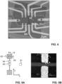
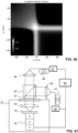
- FIG. 4 An optical micrograph of the resulting heterostructure is shown in Fig. 4 .
- the BG electrode was comparatively large, encompassing almost the entire MoSe 2 flake.
- the TG electrode took the shape of a narrow strip extending along the y direction.
- the TG electrode was optically transparent, allowing to probe optical properties in the region underneath the gate and along its edge.
- the shape of the TG electrode is illustrated in more detail in Fig. 5A .
- a 100 nm wide gap in the TG electrode was created. This gap can be clearly seem in Fig. 5B .
- the TG electrode was contacted from both sides of the gap to have the same electric potential on both sides.
- the semiconductor layer was contacted by several palladium contacts. Some of these contacts were used for doping the semiconductor layer by applying voltages between the BG and TG electrodes and the semiconductor layer. Two of the contacts near opposite ends of the semiconductor flake along the x direction acted as source (S) and drain (D) contacts for studying charge transport along the x direction.
- S source
- D drain
- the global doping level was tuned by applying a BG voltage between the BG electrode and the semiconductor layer.
- the charge carrier density underneath the TG electrode was modified by applying a TG voltage between the TG electrode and the semiconductor layer.
- broadband reflectance and photoluminescence (PL) spectroscopy was performed through a high numerical aperture lens focused at different positions on the sample.
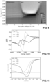
- Fig. 6 typical reflectance spectra as a function of V BG taken at a position away from the TG are shown.
- the beam spot position is marked with a star-symbol in Fig. 4 and is indicated as position 61 in Fig. 5A .
- the doping characteristics of the semiconductor layer are expected to be determined by the BG voltage only, while the effects of the TG voltage are expected to be negligible.
- source-drain transport measurements were performed in the n-doped regime, particularly to characterize the influence of the TG geometry on electronic properties of the semiconductor.
- S-D source-drain
- V BG Fermi energies set by V BG and fixed S-D voltage
- V SD 2 V.
- the fact that the 100 nm wide channel can be completely pinched off at a certain V TG demonstrates that a region of width ⁇ 50 nm around the TG can be completely depleted of electrons.
- V BG corresponding to larger global Fermi energy, the channel pinch-off occurs at more negative V TG .
- V TG As the channel is opened by increasing V TG , a non-linear steplike increase in the current was observed, indicating strong electron confinement in the transverse ( y ) direction of the mesoscopic 1D channel.
- the optical response of the TMD monolayer was measured by positioning the beam spot on the edge of the TG. This position is indicated in Fig. 5A as position 62.
- the measurements corresponded to the combined optical response of three distinct spatial regions: (I) the n-doped region away from the TG that is affected only by the BG, (II) the p-doped region directly underneath the TG, and (III) the narrow i-region between I and II.
- region I Due to the diffraction-limited spot size, the measurements corresponded to the combined optical response of three distinct spatial regions: (I) the n-doped region away from the TG that is affected only by the BG, (II) the p-doped region directly underneath the TG, and (III) the narrow i-region between I and II.
- the contribution of region I to the total optical response remains unchanged as V TG is varied.
- V TG As a function of V TG , the PL counts of each line also decreased with more negative voltage, ultimately becoming too weak to discern for V TG ⁇ -9 V.
- V ( x ) estimates of the corresponding potential ( V ( x ), Eq.(1)) for those voltages as obtained from electrostatic simulations are shown in Fig. 11 .
- the discrete lines were analysed by fitting a superposition of Lorentzian functions to the reflectance spectra.
- the resonance frequencies of the discrete states in reflectance (circles) and PL (diamonds) thus obtained are plotted in Fig. 14 .
- the lowest energy state in reflectance shows a minimum linewidth of ⁇ ⁇ 300 ⁇ eV, which is more than an order of magnitude narrower than the linewidth of the unbound 2D exciton X 0 ( ⁇ ⁇ 4 meV in Fig. 6 ) away from the TG.
- additional fine structure of some of the discrete states at a V TG ⁇ -8 V was observed, the origin of which is not currently understood.
- Fig. 15 the energy E of the resonance lines in the reflectance spectra relative to the energy E cont of the free exciton continuum is plotted as a function of the top gate voltage V TG .
- the continuum energy is the 2D exciton energy in the neutral regime, and the repulsive polaron energy in the doped regime. A simple linear dependence was observed at V TG ⁇ -6 V.
- the dissipation arises from the spatial component of the excitonic wavefunction which leaks into the charged regions.
- the linewidth of the confined states increases up the ladder of states, accompanied by a loss of oscillator strength. It is believed that this is the first example of a trapping mechanism that relies on many-body interactions between a mobile impurity and a surrounding medium. Understanding the dynamics of excitons in such non-Hermitian confining potentials constitutes an interesting problem for future investigations.
- the discrete PL lines appeared as the beam spot crossed the first edge, almost vanished when the beam spot was entirely on the TG, and reappeared as the beam spot crossed the second edge.
- the PL oscillator strength was mainly carried over to the attractive polaron branch.
- the oscillator strength of the lower emission line is shown as a function of space, which shows two peaks separated by about ⁇ 800 nm, in good agreement with the width of the gate when taking into account the measurement uncertainties.
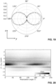
- Figs. 18-21 show linear polarization resolved PL measurements taken at two positions on the sample: Fig. 18 depicts PL from a region which encompasses two parallel TG edges, shown as region 64 in Fig. 5A .
- Fig. 20 shows PL obtained by aligning the beam spot on the split gate (region 65 in Fig. 5A ), which contains two sets of orthogonal wire segments.
- Strongly polarized emission originates from the long-range electron-hole Coulomb exchange in excitons, which results in a coupling between the valley degree of freedom and the center-of-mass exciton motion.
- this coupling can be orders of magnitude greater in TMD monolayers than in III-V semiconductors due to the much larger exciton binding energy in the former.
- the long-range electron-hole exchange coupling leads to an energy splitting between longitudinal and transverse electromagnetic modes.
- the anisotropy of the 1D potential breaks the rotational symmetry and acts as an in-plane Zeeman field on the valley pseudospin, which in turn opens a gap between parallel and perpendicular polarizations even at for momenta within the light cone.
- the localization length scale in the transverse direction (l ⁇ 7 nm) is two orders of magnitude smaller than the wavelength of light, which leads to substantial gap between x and y polarization components.
- FIGs. 25-30 Each of these figures shows, in the respective upper panel, the magnitude of charge density
- the BG voltage V BG was kept at a fixed bias of 4.5 V, while the TG voltage V TG was varied from -2 V to -7 V in steps of 1 V.
- V TG is varied, which can be classified according to the doping state in regions I, II and III.
- Figs. 25-30 show that a confining potential can already be formed in the i-i-n regime, where confinement is solely caused by the dc Stark shift in the inhomogeneous in-plane field, while the repulsive polaron shift due to a spatial modulation of charge density does not yet contribute to confinement.
- the BG electrode 13 covered almost the entire bottom of the semiconductor layer 11, while the TG electrode 15 was structured and partially overlapped with the BG electrode.
- the BG electrode may also be structured.
- a partial overlap of the BG and TG electrodes is advantageous for defining a particularly narrow neutral region between the n- and p-doped regions without requiring lateral alignment of the gate electrodes on a nanometer scale, a partial overlap is not always required.
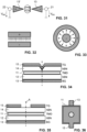
- Fig. 31 shows a possible arrangement of gate electrodes 13, 13' for forming a quantum dot.
- Each gate electrode defines a sharp tip when viewed along a direction perpendicular to the device plane, the tips being arranged opposite to each other.
- Gate voltage sources 21, 22 may provide these electrodes with different voltages V BG and V BG ' relative to the semiconductor layer 11 to create an electric field having a strongly inhomogeneous in-plane component. In this manner, neutral excitons can be confined in zero dimensions in the region between the tips of the gate electrodes.
- a p-doped region may be created below one of the gate electrodes and an n-doped region below the other gate electrode, the p- and n-doped regions being separated by an i-type region, and the resulting polaron shift may enhance confinement.
- the gate electrodes 13, 13' may be arranged in a common plane below the semiconductor layer 11, forming two separate bottom gate electrodes. Alternatively, they may be arranged in a common plane above the semiconductor layer 11, forming two separate top gate electrodes. In both these cases, a further gate electrode may be arranged on the opposite side of the semiconductor layer, e.g., to globally modify the charge carrier density. In yet other embodiments, the gate electrodes 13, 13' may be arranged on opposite sides of the semiconductor layer, allowing their in-plane distance to be minimized.
- Fig. 32 shows a possible arrangement of gate electrodes for confining dipolar in-plane excitons in a 1D channel
- Fig. 33 shows a possible arrangement of gate electrodes for confining dipolar in-plane excitons in an annular region.
- the gate electrodes may be supplied with voltages of different polarities to create strongly inhomogeneous in-plane fields, and optionally to create n- and p-doped regions below the gate electrodes.
- the gate electrodes may be provided in a common plane on one side of the semiconductor layer, or they may be provided on different sides of the semiconductor layer.
- Fig. 34 illustrates another embodiment of a device for confining dipolar in-plane excitons.
- the top gate (TG) electrode 15 is not completely planar, but has a portion that extends into the dielectric spacer layer 14 along the out-of-plane direction, this portion having a pointed shape that defines a tip (e.g., conical or pyramidal shape), the tip being directed towards the semiconductor (TMD) layer 11.
- TMD semiconductor
- a strongly inhomogeneous in-plane electric field results around the tip.
- This in-plane electric field can be modified by providing a flat bottom gate (BG) electrode 15 below the semiconductor layer 11 and applying a voltage between the semiconductor layer 11 and the BG electrode 15.
- BG flat bottom gate
- the BG electrode does not need to be patterned in the region of the pointed portion of the TG electrode.
- the in-plane field may cause differently shaped confining potentials for neutral excitons.
- these voltage can be applied in such a manner that the semiconductor layer is globally n- or p-doped, whereas a small island directly below the tip is depleted of charge carriers (i.e., is of the i type), resulting in a confining potential that has a minimum with respect to both dimensions in the device plane, the minimum being located directly below the tip, thereby enabling exciton confinement in zero dimensions.
- the island directly below the tip may become oppositely doped relative to the surrounding semiconductor layer, resulting in a ring-shaped i-type region and correspondingly in a confinement potential that has the form of a ring-shaped potential well.
- the pointed portion of the TG electrode 15 may be created by patterning the dielectric spacer layer 14 before the electrode layer is deposited onto the spacer layer.
- anisotropic hBN etching may be used for patterning the spacer layer, as explained in more detail in Ref. [1].
- thermal scanning probe lithography for freeform hBN patterning may be used, as explained in more detail in Refs. [2, 3].
- Several individually controllable TG electrodes can readily be created and can be combined into an array.
- a strongly inhomogeneous in-plane electric field can be created by applying a voltage between the TG electrode and the semiconductor layer, and the in-plane electric field can be modified by providing a flat bottom gate (BG) electrode 15 below the semiconductor layer 11 and applying a voltage between the semiconductor layer 11 and the BG electrode 15.
- BG flat bottom gate
- these voltages can be applied in such a manner that the semiconductor layer is globally n- or p-doped, whereas a small island directly below the hole is depleted of charge carriers, resulting in a confining potential that has a minimum with respect to both dimensions in the device plane, the minimum being located directly below the hole, thereby enabling exciton confinement in zero dimensions.
- the voltage asymmetry between the gates is increased, the island directly below the hole may become oppositely doped relative to the surrounding semiconductor layer, resulting in a ring-shaped i-type region and correspondingly in a confinement potential that has the form of a ring-shaped potential well.
- Figs. 37-40 illustrate another possibility for confining excitons in zero dimensions (0D), thereby creating a quantum dot (QD).
- the BG electrode 13 is patterned into a plurality of parallel, individually addressable strips (see Fig. 37 ).
- the TG electrode 15 is also patterned into parallel, individually addressable strips. The TG strips are oriented at an angle to the BG strips, in particular, perpendicular to the BG strips.
- This field has its maximum at the positions where the edges of the TG and BG strips intersect when viewed in a viewing direction that is perpendicular to the device plane.
- a confining potential for confining neutral excitons in zero dimensions is created at each such position (black dots in Fig. 37 ).
- the resulting confinement length scale is determined by the thickness of the dielectric spacer layers and can thus be readily tuned.
- An exciton confined in such a potential acts as a quantum dot (QD).
- QD quantum dot
- the quantum dots can be manipulated by the voltages applied to the corresponding strips.
- Fig. 38 shows an enlarged view of a portion of Fig. 37.
- a region above the BG electrode that is sufficiently removed from the TG electrode is n-doped (dark region in Fig. 39 ).
- a region below the TG electrode that is sufficiently removed from the BG electrode is p-doped (white region in Fig. 39 ).
- An i-type region is present between these doped regions.
- the i-type region is narrowest at the point where the edges of the TG and BG strips intersect.
- the resulting in-plane electric field distribution is illustrated in Fig. 40 .
- the in-plane field has its maximum near the point of intersection and rapidly falls off in all lateral directions away from this point. Thereby a confining potential for 0D confinement is created at the point of intersection.
- An advantage of this embodiment is that an array of quantum dots can be created without requiring high-resolution patterning.
- MoSe 2 were used in the above example as the material for the semiconductor layer, other materials may also be used. While transition metal dichalcogenides are preferred, other classes of layered semiconductor materials may also be used. These include inorganic and organic hybrid perovskites, black phosphorous, bilayer graphene, silicene, antimonene, and some semiconducting polymers.
- the semiconductor layer is a monolayer, this is not strictly required.
- the semiconductor layer may be comprised of more than one layer as long as the semiconductor layer is sufficiently thin.
- the layer structure 11 may comprise two or more thin semiconductor layers separated by a separating layer.
- the device shown in Fig. 4 was fabricated as follows. Device fabrication began by mechanically exfoliating MoSe 2 and hBN flakes from bulk crystals (HQ Graphene MoSe 2 and NIMS h-BN) onto 285 nm SiO 2 substrates using wafer dicing tape (Ultron). The flake thicknesses were identified using optical contrast measurements and/or atomic force microscopy. For the device of Fig. 4 , hBN flakes which are ⁇ 30nm thick were selected. Embedded Via-contacts were formed by etching holes in the hBN spacer layers by means of electron beam lithography and reactive ion etching (Oxford Plasmalab 80Plus).
- the etching conditions were the following: CHF 3 :O 2 40:4 sccm gas mixture, 60 W RF power and 40 mTorr gas pressure.
- the etched hBN layer was transferred to a new Si/SiO 2 substrate using a standard dry polymer transfer method (also used for stacking, see following paragraph).
- the pre-defined holes were filled with metal by performing a second lithography step and (electron-beam) evaporation of 20 nm of Pd and 30 nm of Au.
- the multilayer stack was then created by picking up the top hBN layer with embedded Via- contacts and laminating it onto a monolayer MoSe 2 , and a bottom hBN flake using the aforementioned dry transfer process.
- a glass slide was used, onto which a hemispherical polydimethylsiloxane (PDMS) stamp was attached.
- This stamp was covered with a thin layer of polycarbonate (PC), allowing the sequential pickup of the flakes. All stacking steps were thereby performed in an inert Ar atmosphere inside a glovebox and at a temperature of 120 °C.
- the finished stack was deposited onto the gold bottom gate by increasing the temperature up to 150 °C, which allowed the PC to delaminate from the PDMS and to be released on the substrate. By further heating to 170 °C, the PC was torn at the edges. The PC was dissolved by immersing the substrate in chloroform.
- the bottom gate on the Si/SiO 2 substrate was formed by lithographically defining a square of 20 ⁇ m size and electron-beam evaporating 3 nm of Ti and 10 nm of Au.
- a split top gate electrode was patterned, which was 200 nm wide and included a 100 nm gap, allowing the formation of a gate-defined constriction.
- electron-beam lithography was used to evaporate 3 nm of Ti and 10 nm of Au. This rendered the top gate optically transparent and therefore allowed to probe the optical properties of the monolayer underneath.
- the embedded Via-contacts in the top hBN spacer layer along with top gate were electrically contacted with extended metal electrodes prepared using another lithography step and subsequent evaporation of 5 nm of Ti and 85 nm of Au.
- ultrathin semiconductor layers as well as dielectric insulating layers may be obtained not only by cleavage from a bulk crystal, but also by other methods such as chemical vapor deposition, see, e.g., the paper by C. Tan et al., section 4.7, and that the present invention is not limited to devices fabricated by the above-described methods.
- Optical experiments were carried out in a confocal microscope setup, as schematically illustrated in Fig. 41 .
- the sample was mounted on an xyz piezo-electric stage 32 located inside a stainless steel tube 30, which was immersed in a liquid helium bath cryostat.
- the steel tube 30 was filled with 20 mbar helium exchange gas to maintain a sample temperature of ⁇ 4.2 K. Free-space optical access to the sample was enabled through a glass window 31 on top of the tube 30.
- White light (WL) reflectance and photoluminescence were measured using a broadband light-emitting diode centered at 760 nm and a tunable single-mode Ti:Sapphire laser as the excitation light source 40, respectively.
- the excitation light source 40, the spectrometer 47, and the xyz stage 32 were controlled by control circuitry 50. For WL measurements an excitation power of a few tens of nW, and for PL a few ⁇ W was maintained. The polarization resolved PL measurements were carried out with an angle-scanning polarizer placed in the emission path.
Landscapes
- Junction Field-Effect Transistors (AREA)
Claims (15)
- Verfahren zum lateralen Einschliessen neutraler Exzitonen in einer Halbleiterschichtstruktur (11) einer Festkörpervorrichtung (10), wobei die Halbleiterschichtstruktur (11) mindestens eine Halbleiterschicht umfasst und eine Vorrichtungsebene definiert, wobei das Verfahren umfasst:Erzeugen eines inhomogenen elektrischen Feldes (F) in der Halbleiterschichtstruktur (11), wobei das elektrische Feld (F) eine in der Ebene liegende Feldkomponente (Fx) aufweist, deren Betrag entlang mindestens einer Begrenzungsrichtung (x) in der Vorrichtungsebene variiert, wobei der Betrag der in der Ebene liegenden Feldkomponente (Fx) ein Maximum entlang der Begrenzungsrichtung (x) aufweist, wodurch die in der Ebene liegende Feldkomponente (Fx) ein laterales Begrenzungspotential (V(x)) für neutrale Exzitonen um das Maximum herum verursacht; undBestrahlung der Festkörpervorrichtung (10) mit Licht, um neutrale Exzitonen in der Halbleiterschichtstruktur (11) zu erzeugen, wobei die neutralen Exzitonen durch das laterale Begrenzungspotential (V(x)) entlang der Begrenzungsrichtung (x) lateral eingeschlossen werden.
- Verfahren nach Anspruch 1,wobei das Erzeugen des inhomogenen elektrischen Feldes (F) in der Halbleiterschichtstruktur (11) das Modifizieren einer Ladungsträgerdichte (σ) in der Halbleiterschichtstruktur (11) umfasst, um einen p-dotierten Bereich (16) und/oder einen n-dotierten Bereich (18) zu erzeugen,insbesondere, wobei sowohl ein p-dotierter Bereich (16) als auch ein n-dotierter Bereich (18) erzeugt werden, wobei der p-dotierte Bereich (16) und der n-dotierte Bereich in der Vorrichtungsebene durch einen i-Typ-Bereich (17) lateral getrennt sind, wobei das Maximum des Betrags der in der Ebene liegenden Feldkomponente (Fx) in dem i-Typ-Bereich (17) zwischen dem p-dotierten Bereich (16) und dem n-dotierten Bereich (18) liegt, wodurch die neutralen Exzitonen in dem i-Typ-Bereich (17) lateral eingeschlossen sind.
- Verfahren nach Anspruch 2,wobei das Modifizieren der Ladungsträgerdichte (σ) in der Halbleiterschichtstruktur (11) eine chemische Dotierung mindestens eines Teils der Halbleiterschichtstruktur (11) umfasst, und/oderwobei das Modifizieren der Ladungsträgerdichte (σ) in der Halbleiterschichtstruktur (11) das Anlegen mindestens einer Gate-Spannung zwischen mindestens einer Gate-Elektrode (13; 13'; 15) und der Halbleiterschichtstruktur (11) umfasst.
- Verfahren nach einem der vorhergehenden Ansprüche,wobei die Festkörpervorrichtung (10) eine isolierende erste Abstandshalterschicht (12), die auf einer ersten Oberfläche der Halbleiterschichtstruktur (11) angeordnet ist, und eine erste Gate-Elektrode (13), die auf der ersten Abstandshalterschicht (12) angeordnet ist, umfasst, undwobei das Erzeugen des inhomogenen elektrischen Feldes (F) das Anlegen einer ersten Gate-Spannung (VBG ) zwischen der ersten Gate-Elektrode (13) und der Halbleiterschichtstruktur (11) umfasst.
- Verfahren nach Anspruch 4,wobei die Festkörpervorrichtung (10) ferner eine zweite Gate-Elektrode (15) umfasst, die auf der ersten Abstandshalterschicht (12) oder auf einer isolierenden zweiten Abstandshalterschicht (14) angeordnet ist, die zwischen der Halbleiterschichtstruktur (11) und der zweiten Gate-Elektrode (15) auf einer zweiten Oberfläche der Halbleiterschichtstruktur (11) gegenüber der ersten Abstandshalterschicht (12) angeordnet ist,wobei das Erzeugen des inhomogenen elektrischen Feldes (F) in der Halbleiterschichtstruktur (11) das Anlegen einer zweiten Gate-Spannung (VTG ) zwischen der zweiten Gate-Elektrode (15) und der Halbleiterschichtstruktur (11), wobei die ersten und zweiten Gate-Spannungen (VBG, VTG ) entgegengesetzte Vorzeichen haben,insbesondere, wobei die zweite Gate-Elektrode (15) auf der zweiten Abstandshalterschicht (14) angeordnet ist und sich mit der ersten Gate-Elektrode (13) teilweise überlappt, wenn entlang einer aus der Ebene herausragenden Richtung (z) betrachtet, die senkrecht zur Vorrichtungsebene ist.
- Verfahren nach einem der vorhergehenden Ansprüche,wobei das Maximum des Betrages der in der Ebene liegenden Feldkomponente (Fx) mindestens 10 V/µm beträgt, und/oderwobei die in der Ebene liegende Feldkomponente (Fx) als Funktion der Position (x) entlang der Begrenzungsrichtung eine Kurve mit einer Halbwertsbreite (FWHM) von nicht mehr als 100 nm beschreibt.
- Verfahren nach einem der vorhergehenden Ansprüche,wobei die mindestens eine Halbleiterschicht in der Halbleiterschichtstruktur (11) eine Dicke aufweist, die bewirkt, dass die elektrische Polarisierbarkeit von Exzitonen senkrecht zur Vorrichtungsebene nicht mehr als 10 % der elektrischen Polarisierbarkeit von Exzitonen in der Vorrichtungsebene beträgt, und/oderwobei die Halbleiterschicht eine Dicke von nicht mehr als 5 nm aufweist, und/oderwobei Exzitonen in der Halbleiterschichtstruktur (11) eine Bindungsenergie von mindestens 10 meV, vorzugsweise von mindestens 50 meV, aufweisen, und/oderwobei die Halbleiterschichtstruktur (11) ein Halbleitermaterial umfasst, das aus der Gruppe ausgewählt ist, die aus Übergangsmetalldichalkogeniden, anorganischen und organischen Hybridperowskiten, schwarzem Phosphor, zweilagiges Graphen, Silicen, Antimonen und halbleitenden Polymeren besteht,wobei die Halbleiterschichtstruktur (11) vorzugsweise eine Übergangsmetalldichalkogenid-Monolage umfasst.
- Verfahren nach einem der vorhergehenden Ansprüche, wobei die Festkörpervorrichtung (10) bei einer Temperatur betrieben wird, bei der die Exzitonen ein Verhältnis zwischen Bindungsenergie und Linienbreite im lateralen Begrenzungspotential (V(x)) von mindestens 10 aufweisen.
- Verfahren nach einem der vorhergehenden Ansprüche, wobei das laterale Begrenzungspotential (V(x)) bewirkt, dass die Exzitonen mindestens zwei gebundene Bewegungseigenzustände in dem lateralen Begrenzungspotential (V(x)) aufweisen, wobei die Eigenzustände vorzugsweise durch eine Energiespaltung von mindestens 0,5 meV getrennt sind.
- Vorrichtung zum lateralen Einschliessen neutraler Exzitonen, wobei die Vorrichtung umfasst:eine Halbleiterschichtstruktur (11), die eine Vorrichtungsebene definiert;eine isolierende erste Abstandshalterschicht (12), die auf einer ersten Oberfläche der Halbleiterschichtstruktur (11) angeordnet ist;eine erste Gate-Elektrode (13), die auf der ersten Abstandshalterschicht (12) angeordnet ist;eine zweite Gate-Elektrode (15; 13'), die auf der ersten Abstandshalterschicht (14) oder auf einer isolierenden zweiten Abstandshalterschicht (14) angeordnet ist, die zwischen der Halbleiterschichtstruktur (11) und der zweiten Gate-Elektrode (15) auf einer zweiten Oberfläche der Halbleiterschichtstruktur (11) gegenüber der ersten Abstandshalterschicht (12) angeordnet ist;eine erste Spannungsquelle (21), die dazu ausgebildet ist, eine erste Gate-Spannung (VBG ) zwischen der ersten Gate-Elektrode (13) und der Halbleiterschichtstruktur (11) anzulegen; undeine zweite Spannungsquelle (22), die dazu ausgebildet ist, eine zweite Gate-Spannung (VTG; VBG') zwischen der zweiten Gate-Elektrode (15; 13') und der Halbleiterschichtstruktur (11) anzulegen,wobei die erste und zweite Gate-Elektrode (13; 13'; 15) so angeordnet sind und die erste und die zweite Spannungsquelle (21, 22) dazu ausgebildet sind, die erste und die zweite Gate-Spannung mit solchen Polaritäten und Beträgen anzulegen, dass in der Halbleiterschichtstruktur (11) ein inhomogenes elektrisches Feld (F) erzeugt wird, wobei das elektrische Feld (F) eine in der Ebene liegende Feldkomponente (Fx) aufweist, deren Betrag entlang mindestens einer Begrenzungsrichtung in der Vorrichtungsebene variiert, wobei der Betrag der in der Ebene liegenden Feldkomponente (Fx) ein Maximum entlang der Begrenzungsrichtung aufweist, wodurch die in der Ebene liegende Feldkomponente (Fx) ein laterales Begrenzungspotential (V(x)) für neutrale Exzitonen um das Maximum herum verursacht.
- Vorrichtung nach Anspruch 10, wobei die zweite Gate-Elektrode (15) auf der zweiten Abstandshalterschicht (14) angeordnet ist und sich teilweise mit der ersten Gate-Elektrode (13) überlappt, wenn entlang einer aus der Ebene herausragenden Richtung (z) betrachtet, die senkrecht zur Vorrichtungsebene ist.
- Vorrichtung nach Anspruch 11,
wobei die erste und die zweite Spannungsquelle (21, 22) dazu ausgebildet sind, die erste und die zweite Gate-Spannung mit solchen Polaritäten und Beträgen anzulegen, dass in der Halbleiterschichtstruktur (11) in einem Bereich der ersten Gate-Elektrode (13), in dem keine Überlappung mit der zweiten Gate-Elektrode (15) besteht, ein n- oder p-dotierter Bereich erzeugt wird und in einem Überlappungsbereich ein entgegengesetzt dotierter Bereich erzeugt wird, so dass sich an einem Rand des Überlappungsbereichs entlang des Umfangs der zweiten Gate-Elektrode (15) ein i-Typ-Bereich bildet. - Vorrichtung nach Anspruch 11,wobei die erste Gate-Elektrode (13) einen ersten Rand aufweist, der sich in einer ersten Richtung erstreckt, wobei die zweite Gate-Elektrode (15) einen zweite Rand aufweist, der sich in einer zweiten Richtung erstreckt, wobei die erste und die zweite Richtung unterschiedlich und vorzugsweise orthogonal sind, und wobei die erste und die zweite Spannungsquelle (21, 22) dazu ausgebildet sind, die erste und die zweite Gate-Spannung mit solchen Polaritäten und Beträgen anzulegen, dass das resultierende laterale Begrenzungspotential (V(x)) ein Minimum in Bezug auf zwei Dimensionen in der Vorrichtungsebene in der Nähe einer Position hat, an der sich der erste und der zweite Rand schneiden, wenn entlang einer aus der Ebene herausragenden Richtung (z) betrachtet, die senkrecht zu der Vorrichtungsebene ist, so dass Exzitonen in Null-Dimensionen eingegrenzt werden, oderwobei die zweite Gate-Elektrode (15) einen Abschnitt aufweist, der sich in die zweite Abstandshalterschicht (14) entlang einer aus der Ebene herausragenden Richtung (z) senkrecht zur Vorrichtungsebene erstreckt, wobei der Abschnitt zu einer Spitze konvergiert, wobei die Spitze auf die Halbleiterschichtstruktur (11) gerichtet ist, und wobei die erste und die zweite Spannungsquelle (21, 22) dazu ausgebildet sind, die erste und die zweite Gate-Spannung mit solchen Polaritäten und Beträgen anzulegen, dass das resultierende laterale Begrenzungspotential (V(x)) ein Minimum in Bezug auf zwei Dimensionen in der Vorrichtungsebene aufweist, um Exzitonen in Null-Dimensionen einzuschliessen, oder dass das laterale Begrenzungspotential (V(x)) einen ringförmigen Potentialtopf um die Spitze herum bildet, so dass Exzitonen in einer Dimension in einem ringförmigen Bereich eingeschlossen werden; oderwobei die zweite Gate-Elektrode (15) ein kreisförmiges Loch aufweist, und wobei die erste und die zweite Spannungsquelle (21, 22) dazu ausgebildet sind, die erste und die zweite Gate-Spannung mit solchen Polaritäten und Beträgen anzulegen, dass das resultierende laterale Begrenzungspotenzial (V(x)) ein Minimum in Bezug auf zwei Dimensionen in der Vorrichtungsebene aufweist, um Exzitonen in Null-Dimensionen einzuschliessen, oder dass das laterale Begrenzungspotential (V(x)) einen ringförmigen Potentialtopf entlang eines Rands des Lochs bildet, so dass Exzitonen in einer Dimension in einem ringförmigen Bereich eingeschlossen werden.
- Vorrichtung nach einem der Ansprüche 10-13,wobei Exzitonen in der Halbleiterschichtstruktur (11) eine Bindungsenergie von mindestens 10 meV, vorzugsweise von mindestens 100 meV, aufweisen,wobei die Halbleiterschichtstruktur (11) vorzugsweise eine Übergangsmetalldichalkogenid-Monolage umfasst.
- Vorrichtung nach einem der Ansprüche 10-14, die ferner ein optisches System (41-44) umfasst, das dazu ausgebildet ist, die Halbleiterschichtstruktur (11) mit einfallendem Licht zu bestrahlen, um neutrale Exzitonen in der Halbleiterschichtstruktur (11) anzuregen.
Applications Claiming Priority (2)
| Application Number | Priority Date | Filing Date | Title |
|---|---|---|---|
| EP21156970.2A EP4044261A1 (de) | 2021-02-12 | 2021-02-12 | Begrenzung von neutralen exzitonen in einer halbleiterschichtstruktur |
| PCT/EP2022/053327 WO2022171778A1 (en) | 2021-02-12 | 2022-02-11 | Confinement of neutral excitons in a semiconductor layer structure |
Publications (2)
| Publication Number | Publication Date |
|---|---|
| EP4292137A1 EP4292137A1 (de) | 2023-12-20 |
| EP4292137B1 true EP4292137B1 (de) | 2024-12-18 |
Family
ID=74625808
Family Applications (2)
| Application Number | Title | Priority Date | Filing Date |
|---|---|---|---|
| EP21156970.2A Withdrawn EP4044261A1 (de) | 2021-02-12 | 2021-02-12 | Begrenzung von neutralen exzitonen in einer halbleiterschichtstruktur |
| EP22708840.8A Active EP4292137B1 (de) | 2021-02-12 | 2022-02-11 | Begrenzung von neutralen exzitonen in einer halbleiterschichtstruktur |
Family Applications Before (1)
| Application Number | Title | Priority Date | Filing Date |
|---|---|---|---|
| EP21156970.2A Withdrawn EP4044261A1 (de) | 2021-02-12 | 2021-02-12 | Begrenzung von neutralen exzitonen in einer halbleiterschichtstruktur |
Country Status (3)
| Country | Link |
|---|---|
| US (1) | US20240128395A1 (de) |
| EP (2) | EP4044261A1 (de) |
| WO (1) | WO2022171778A1 (de) |
Families Citing this family (2)
| Publication number | Priority date | Publication date | Assignee | Title |
|---|---|---|---|---|
| EP4095602A1 (de) * | 2021-05-27 | 2022-11-30 | ETH Zurich | Verfahren zur herstellung eines nanostrukturierten elements aus hexagonalem bornitrid und vorrichtung mit einem solchen element |
| WO2025111298A1 (en) * | 2023-11-22 | 2025-05-30 | Northwestern University | Moiré synaptic transistors and applications of same |
Family Cites Families (6)
| Publication number | Priority date | Publication date | Assignee | Title |
|---|---|---|---|---|
| US7825402B2 (en) | 2006-03-27 | 2010-11-02 | The Regents Of The University Of California | Excitonic signal processing optically interfaced electrically controlled devices |
| JP4258527B2 (ja) | 2006-04-28 | 2009-04-30 | トヨタ自動車株式会社 | 車両の排気熱回収装置の取付構造 |
| GB201612419D0 (en) | 2016-07-18 | 2016-08-31 | Cambridge Entpr Ltd | A scalable quantum-confined device |
| ES2792076T3 (es) | 2017-02-08 | 2020-11-10 | Consejo Superior Investigacion | Dispositivo monolítico fuente de luz cuántica ajustable y circuito óptico cuántico del mismo |
| US20210217919A1 (en) * | 2018-05-28 | 2021-07-15 | Ecole Polytechnique Federale De Lausanne (Epfl) | Excitonic device and operating methods thereof |
| KR102045064B1 (ko) | 2018-09-20 | 2019-11-14 | 울산과학기술원 | 양자 광원 및 그 제조 방법 |
-
2021
- 2021-02-12 EP EP21156970.2A patent/EP4044261A1/de not_active Withdrawn
-
2022
- 2022-02-11 EP EP22708840.8A patent/EP4292137B1/de active Active
- 2022-02-11 US US18/277,017 patent/US20240128395A1/en active Pending
- 2022-02-11 WO PCT/EP2022/053327 patent/WO2022171778A1/en not_active Ceased
Non-Patent Citations (3)
| Title |
|---|
| GIOVANNI SCURI ET AL: "Electrically tunable valley dynamics in twisted WSe_2/WSe_2 bilayers", ARXIV.ORG, CORNELL UNIVERSITY LIBRARY, 201 OLIN LIBRARY CORNELL UNIVERSITY ITHACA, NY 14853, 24 December 2019 (2019-12-24), XP081563972 * |
| HYEONJUN BAEK ET AL: "Highly tunable quantum light from moire trapped excitons", ARXIV.ORG, CORNELL UNIVERSITY LIBRARY, 201 OLIN LIBRARY CORNELL UNIVERSITY ITHACA, NY 14853, 13 January 2020 (2020-01-13), XP081576508 * |
| NADINE LEISGANG ET AL: "Giant Stark splitting of an exciton in bilayer MoS_2", ARXIV.ORG, CORNELL UNIVERSITY LIBRARY, 201 OLIN LIBRARY CORNELL UNIVERSITY ITHACA, NY 14853, 6 February 2020 (2020-02-06), XP081594165 * |
Also Published As
| Publication number | Publication date |
|---|---|
| WO2022171778A1 (en) | 2022-08-18 |
| EP4292137A1 (de) | 2023-12-20 |
| US20240128395A1 (en) | 2024-04-18 |
| EP4044261A1 (de) | 2022-08-17 |
Similar Documents
| Publication | Publication Date | Title |
|---|---|---|
| Andersen et al. | Excitons in a reconstructed moiré potential in twisted WSe2/WSe2 homobilayers | |
| Sun et al. | Twisted van der Waals quantum materials: fundamentals, tunability, and applications | |
| Rivera et al. | Interlayer valley excitons in heterobilayers of transition metal dichalcogenides | |
| CN109844969B (zh) | 可扩展量子限制装置 | |
| Bai et al. | Evidence for exciton crystals in a 2D semiconductor heterotrilayer | |
| RU2565336C2 (ru) | Легирование графена дырками | |
| Funk et al. | High mobility one-and two-dimensional electron systems in nanowire-based quantum heterostructures | |
| Ogletree et al. | Revealing optical properties of reduced‐dimensionality materials at relevant length scales | |
| Liljeroth et al. | Can scanning tunnelling spectroscopy measure the density of states of semiconductor quantum dots? | |
| Karpińska et al. | Interlayer excitons in MoSe2/2D perovskite hybrid heterostructures–the interplay between charge and energy transfer | |
| US20240128395A1 (en) | Confinement of neutral excitons in a semiconductor layer structure | |
| Jung et al. | Highly tensile-strained Ge/InAlAs nanocomposites | |
| Brotons-Gisbert et al. | Interlayer and Moiré excitons in atomically thin double layers: From individual quantum emitters to degenerate ensembles: M. Brotons-Gisbert et al. | |
| Descamps et al. | Semiconductor membranes for electrostatic exciton trapping in optically addressable quantum transport devices | |
| Bao et al. | Exciton Emission Enhancement in Two-Dimensional Monolayer Tungsten Disulfide on a Silicon Substrate via a Fabry–Pérot Microcavity | |
| Geng et al. | Imaging valley excitons in a 2D semiconductor with scanning tunneling microscope-induced luminescence | |
| Wei et al. | Valley polarization in size-tunable monolayer semiconductor quantum dots | |
| Thureja et al. | Tunable quantum confinement of neutral excitons using electric fields and exciton-charge interactions | |
| Crea | Two-dimensional electro-optic device integrated on plasmonic gold nanostructures | |
| Mazumder | Optoelectronic properties of the two-dimensional van der Waals semiconductor indium selenide (InSe) | |
| Zhu | Electrically Driven Plasmonic Processes: Hot Carriers and Strong Coupling | |
| Nguyen | Toward THz-driven electron in graphene: Field emission & floating-gate tunneling devices | |
| Lamsaadi | Neutral exciton manipulation in transition metal dichalcogenide heterostructures | |
| Li | Fabrication, Characterization, and Device Applications of Few-Layer Black Phosphorus | |
| Ramirez et al. | Electron–hole symmetry breakings in optical fine structures of single self-assembled quantum dots |
Legal Events
| Date | Code | Title | Description |
|---|---|---|---|
| STAA | Information on the status of an ep patent application or granted ep patent |
Free format text: STATUS: UNKNOWN |
|
| STAA | Information on the status of an ep patent application or granted ep patent |
Free format text: STATUS: THE INTERNATIONAL PUBLICATION HAS BEEN MADE |
|
| PUAI | Public reference made under article 153(3) epc to a published international application that has entered the european phase |
Free format text: ORIGINAL CODE: 0009012 |
|
| STAA | Information on the status of an ep patent application or granted ep patent |
Free format text: STATUS: REQUEST FOR EXAMINATION WAS MADE |
|
| 17P | Request for examination filed |
Effective date: 20230825 |
|
| AK | Designated contracting states |
Kind code of ref document: A1 Designated state(s): AL AT BE BG CH CY CZ DE DK EE ES FI FR GB GR HR HU IE IS IT LI LT LU LV MC MK MT NL NO PL PT RO RS SE SI SK SM TR |
|
| DAV | Request for validation of the european patent (deleted) | ||
| DAX | Request for extension of the european patent (deleted) | ||
| GRAP | Despatch of communication of intention to grant a patent |
Free format text: ORIGINAL CODE: EPIDOSNIGR1 |
|
| STAA | Information on the status of an ep patent application or granted ep patent |
Free format text: STATUS: GRANT OF PATENT IS INTENDED |
|
| INTG | Intention to grant announced |
Effective date: 20240711 |
|
| GRAS | Grant fee paid |
Free format text: ORIGINAL CODE: EPIDOSNIGR3 |
|
| GRAA | (expected) grant |
Free format text: ORIGINAL CODE: 0009210 |
|
| STAA | Information on the status of an ep patent application or granted ep patent |
Free format text: STATUS: THE PATENT HAS BEEN GRANTED |
|
| REG | Reference to a national code |
Ref country code: DE Ref legal event code: R081 Ref document number: 602022008854 Country of ref document: DE Owner name: ETH ZURICH, CH Free format text: FORMER OWNER: ANMELDERANGABEN UNKLAR / UNVOLLSTAENDIG, 80297 MUENCHEN, DE |
|
| AK | Designated contracting states |
Kind code of ref document: B1 Designated state(s): AL AT BE BG CH CY CZ DE DK EE ES FI FR GB GR HR HU IE IS IT LI LT LU LV MC MK MT NL NO PL PT RO RS SE SI SK SM TR |
|
| REG | Reference to a national code |
Ref country code: CH Ref legal event code: EP |
|
| REG | Reference to a national code |
Ref country code: DE Ref legal event code: R096 Ref document number: 602022008854 Country of ref document: DE |
|
| REG | Reference to a national code |
Ref country code: IE Ref legal event code: FG4D |
|
| REG | Reference to a national code |
Ref country code: DE Ref document number: 602022008854 Ref country code: DE Ref legal event code: R082 Ref document number: 602022008854 Country of ref document: DE Representative=s name: PATENTANWAELTE OLBRICHT, BUCHHOLD, KEULERTZ PA, DE |
|
| REG | Reference to a national code |
Ref country code: DE Ref legal event code: R082 Ref document number: 602022008854 Country of ref document: DE Representative=s name: PATENTANWAELTE OLBRICHT, BUCHHOLD, KEULERTZ PA, DE |
|
| REG | Reference to a national code |
Ref country code: LT Ref legal event code: MG9D |
|
| PG25 | Lapsed in a contracting state [announced via postgrant information from national office to epo] |
Ref country code: HR Free format text: LAPSE BECAUSE OF FAILURE TO SUBMIT A TRANSLATION OF THE DESCRIPTION OR TO PAY THE FEE WITHIN THE PRESCRIBED TIME-LIMIT Effective date: 20241218 |
|
| PGFP | Annual fee paid to national office [announced via postgrant information from national office to epo] |
Ref country code: DE Payment date: 20250218 Year of fee payment: 4 |
|
| PG25 | Lapsed in a contracting state [announced via postgrant information from national office to epo] |
Ref country code: FI Free format text: LAPSE BECAUSE OF FAILURE TO SUBMIT A TRANSLATION OF THE DESCRIPTION OR TO PAY THE FEE WITHIN THE PRESCRIBED TIME-LIMIT Effective date: 20241218 |
|
| PG25 | Lapsed in a contracting state [announced via postgrant information from national office to epo] |
Ref country code: BG Free format text: LAPSE BECAUSE OF FAILURE TO SUBMIT A TRANSLATION OF THE DESCRIPTION OR TO PAY THE FEE WITHIN THE PRESCRIBED TIME-LIMIT Effective date: 20241218 |
|
| PG25 | Lapsed in a contracting state [announced via postgrant information from national office to epo] |
Ref country code: NO Free format text: LAPSE BECAUSE OF FAILURE TO SUBMIT A TRANSLATION OF THE DESCRIPTION OR TO PAY THE FEE WITHIN THE PRESCRIBED TIME-LIMIT Effective date: 20250318 |
|
| REG | Reference to a national code |
Ref country code: NL Ref legal event code: MP Effective date: 20241218 |
|
| PG25 | Lapsed in a contracting state [announced via postgrant information from national office to epo] |
Ref country code: GR Free format text: LAPSE BECAUSE OF FAILURE TO SUBMIT A TRANSLATION OF THE DESCRIPTION OR TO PAY THE FEE WITHIN THE PRESCRIBED TIME-LIMIT Effective date: 20250319 Ref country code: LV Free format text: LAPSE BECAUSE OF FAILURE TO SUBMIT A TRANSLATION OF THE DESCRIPTION OR TO PAY THE FEE WITHIN THE PRESCRIBED TIME-LIMIT Effective date: 20241218 |
|
| PGFP | Annual fee paid to national office [announced via postgrant information from national office to epo] |
Ref country code: CH Payment date: 20250301 Year of fee payment: 4 |
|
| PGFP | Annual fee paid to national office [announced via postgrant information from national office to epo] |
Ref country code: FR Payment date: 20250224 Year of fee payment: 4 |
|
| PG25 | Lapsed in a contracting state [announced via postgrant information from national office to epo] |
Ref country code: RS Free format text: LAPSE BECAUSE OF FAILURE TO SUBMIT A TRANSLATION OF THE DESCRIPTION OR TO PAY THE FEE WITHIN THE PRESCRIBED TIME-LIMIT Effective date: 20250318 |
|
| PG25 | Lapsed in a contracting state [announced via postgrant information from national office to epo] |
Ref country code: NL Free format text: LAPSE BECAUSE OF FAILURE TO SUBMIT A TRANSLATION OF THE DESCRIPTION OR TO PAY THE FEE WITHIN THE PRESCRIBED TIME-LIMIT Effective date: 20241218 |
|
| REG | Reference to a national code |
Ref country code: AT Ref legal event code: MK05 Ref document number: 1752974 Country of ref document: AT Kind code of ref document: T Effective date: 20241218 |
|
| PG25 | Lapsed in a contracting state [announced via postgrant information from national office to epo] |
Ref country code: SM Free format text: LAPSE BECAUSE OF FAILURE TO SUBMIT A TRANSLATION OF THE DESCRIPTION OR TO PAY THE FEE WITHIN THE PRESCRIBED TIME-LIMIT Effective date: 20241218 |
|
| PG25 | Lapsed in a contracting state [announced via postgrant information from national office to epo] |
Ref country code: PL Free format text: LAPSE BECAUSE OF FAILURE TO SUBMIT A TRANSLATION OF THE DESCRIPTION OR TO PAY THE FEE WITHIN THE PRESCRIBED TIME-LIMIT Effective date: 20241218 |
|
| PG25 | Lapsed in a contracting state [announced via postgrant information from national office to epo] |
Ref country code: ES Free format text: LAPSE BECAUSE OF FAILURE TO SUBMIT A TRANSLATION OF THE DESCRIPTION OR TO PAY THE FEE WITHIN THE PRESCRIBED TIME-LIMIT Effective date: 20241218 |
|
| PG25 | Lapsed in a contracting state [announced via postgrant information from national office to epo] |
Ref country code: IS Free format text: LAPSE BECAUSE OF FAILURE TO SUBMIT A TRANSLATION OF THE DESCRIPTION OR TO PAY THE FEE WITHIN THE PRESCRIBED TIME-LIMIT Effective date: 20250418 |
|
| PG25 | Lapsed in a contracting state [announced via postgrant information from national office to epo] |
Ref country code: PT Free format text: LAPSE BECAUSE OF FAILURE TO SUBMIT A TRANSLATION OF THE DESCRIPTION OR TO PAY THE FEE WITHIN THE PRESCRIBED TIME-LIMIT Effective date: 20250421 |
|
| PG25 | Lapsed in a contracting state [announced via postgrant information from national office to epo] |
Ref country code: EE Free format text: LAPSE BECAUSE OF FAILURE TO SUBMIT A TRANSLATION OF THE DESCRIPTION OR TO PAY THE FEE WITHIN THE PRESCRIBED TIME-LIMIT Effective date: 20241218 |
|
| PG25 | Lapsed in a contracting state [announced via postgrant information from national office to epo] |
Ref country code: AT Free format text: LAPSE BECAUSE OF FAILURE TO SUBMIT A TRANSLATION OF THE DESCRIPTION OR TO PAY THE FEE WITHIN THE PRESCRIBED TIME-LIMIT Effective date: 20241218 Ref country code: RO Free format text: LAPSE BECAUSE OF FAILURE TO SUBMIT A TRANSLATION OF THE DESCRIPTION OR TO PAY THE FEE WITHIN THE PRESCRIBED TIME-LIMIT Effective date: 20241218 |
|
| PG25 | Lapsed in a contracting state [announced via postgrant information from national office to epo] |
Ref country code: SK Free format text: LAPSE BECAUSE OF FAILURE TO SUBMIT A TRANSLATION OF THE DESCRIPTION OR TO PAY THE FEE WITHIN THE PRESCRIBED TIME-LIMIT Effective date: 20241218 |
|
| PG25 | Lapsed in a contracting state [announced via postgrant information from national office to epo] |
Ref country code: CZ Free format text: LAPSE BECAUSE OF FAILURE TO SUBMIT A TRANSLATION OF THE DESCRIPTION OR TO PAY THE FEE WITHIN THE PRESCRIBED TIME-LIMIT Effective date: 20241218 |
|
| PG25 | Lapsed in a contracting state [announced via postgrant information from national office to epo] |
Ref country code: IT Free format text: LAPSE BECAUSE OF FAILURE TO SUBMIT A TRANSLATION OF THE DESCRIPTION OR TO PAY THE FEE WITHIN THE PRESCRIBED TIME-LIMIT Effective date: 20241218 |
|
| PG25 | Lapsed in a contracting state [announced via postgrant information from national office to epo] |
Ref country code: SE Free format text: LAPSE BECAUSE OF FAILURE TO SUBMIT A TRANSLATION OF THE DESCRIPTION OR TO PAY THE FEE WITHIN THE PRESCRIBED TIME-LIMIT Effective date: 20241218 |
|
| PG25 | Lapsed in a contracting state [announced via postgrant information from national office to epo] |
Ref country code: MC Free format text: LAPSE BECAUSE OF FAILURE TO SUBMIT A TRANSLATION OF THE DESCRIPTION OR TO PAY THE FEE WITHIN THE PRESCRIBED TIME-LIMIT Effective date: 20241218 |
|
| REG | Reference to a national code |
Ref country code: DE Ref legal event code: R097 Ref document number: 602022008854 Country of ref document: DE |
|
| PG25 | Lapsed in a contracting state [announced via postgrant information from national office to epo] |
Ref country code: DK Free format text: LAPSE BECAUSE OF FAILURE TO SUBMIT A TRANSLATION OF THE DESCRIPTION OR TO PAY THE FEE WITHIN THE PRESCRIBED TIME-LIMIT Effective date: 20241218 |
|
| PG25 | Lapsed in a contracting state [announced via postgrant information from national office to epo] |
Ref country code: LU Free format text: LAPSE BECAUSE OF NON-PAYMENT OF DUE FEES Effective date: 20250211 |
|
| PLBE | No opposition filed within time limit |
Free format text: ORIGINAL CODE: 0009261 |
|
| STAA | Information on the status of an ep patent application or granted ep patent |
Free format text: STATUS: NO OPPOSITION FILED WITHIN TIME LIMIT |
|
| 26N | No opposition filed |
Effective date: 20250919 |
|
| REG | Reference to a national code |
Ref country code: BE Ref legal event code: MM Effective date: 20250228 |
|
| PG25 | Lapsed in a contracting state [announced via postgrant information from national office to epo] |
Ref country code: BE Free format text: LAPSE BECAUSE OF NON-PAYMENT OF DUE FEES Effective date: 20250228 |
|
| PG25 | Lapsed in a contracting state [announced via postgrant information from national office to epo] |
Ref country code: IE Free format text: LAPSE BECAUSE OF NON-PAYMENT OF DUE FEES Effective date: 20250211 |
|
| PG25 | Lapsed in a contracting state [announced via postgrant information from national office to epo] |
Ref country code: CY Free format text: LAPSE BECAUSE OF FAILURE TO SUBMIT A TRANSLATION OF THE DESCRIPTION OR TO PAY THE FEE WITHIN THE PRESCRIBED TIME-LIMIT Effective date: 20241218 |
|
| PG25 | Lapsed in a contracting state [announced via postgrant information from national office to epo] |
Ref country code: LT Free format text: LAPSE BECAUSE OF FAILURE TO SUBMIT A TRANSLATION OF THE DESCRIPTION OR TO PAY THE FEE WITHIN THE PRESCRIBED TIME-LIMIT Effective date: 20241218 |
|
| PG25 | Lapsed in a contracting state [announced via postgrant information from national office to epo] |
Ref country code: TR Free format text: LAPSE BECAUSE OF FAILURE TO SUBMIT A TRANSLATION OF THE DESCRIPTION OR TO PAY THE FEE WITHIN THE PRESCRIBED TIME-LIMIT Effective date: 20241218 |