EP4297109A1 - Thermoelectric conversion device - Google Patents
Thermoelectric conversion device Download PDFInfo
- Publication number
- EP4297109A1 EP4297109A1 EP22756150.3A EP22756150A EP4297109A1 EP 4297109 A1 EP4297109 A1 EP 4297109A1 EP 22756150 A EP22756150 A EP 22756150A EP 4297109 A1 EP4297109 A1 EP 4297109A1
- Authority
- EP
- European Patent Office
- Prior art keywords
- layers
- thermoelectric
- insulating layer
- thermally conductive
- layer
- Prior art date
- Legal status (The legal status is an assumption and is not a legal conclusion. Google has not performed a legal analysis and makes no representation as to the accuracy of the status listed.)
- Granted
Links
Images


Classifications
-
- H—ELECTRICITY
- H10—SEMICONDUCTOR DEVICES; ELECTRIC SOLID-STATE DEVICES NOT OTHERWISE PROVIDED FOR
- H10N—ELECTRIC SOLID-STATE DEVICES NOT OTHERWISE PROVIDED FOR
- H10N10/00—Thermoelectric devices comprising a junction of dissimilar materials, i.e. devices exhibiting Seebeck or Peltier effects
- H10N10/10—Thermoelectric devices comprising a junction of dissimilar materials, i.e. devices exhibiting Seebeck or Peltier effects operating with only the Peltier or Seebeck effects
- H10N10/17—Thermoelectric devices comprising a junction of dissimilar materials, i.e. devices exhibiting Seebeck or Peltier effects operating with only the Peltier or Seebeck effects characterised by the structure or configuration of the cell or thermocouple forming the device
-
- H—ELECTRICITY
- H10—SEMICONDUCTOR DEVICES; ELECTRIC SOLID-STATE DEVICES NOT OTHERWISE PROVIDED FOR
- H10N—ELECTRIC SOLID-STATE DEVICES NOT OTHERWISE PROVIDED FOR
- H10N10/00—Thermoelectric devices comprising a junction of dissimilar materials, i.e. devices exhibiting Seebeck or Peltier effects
- H10N10/80—Constructional details
- H10N10/82—Interconnections
Definitions
- the present invention relates to a thermoelectric conversion device.
- thermoelectric layers made of a thermoelectric material and connection layers for connecting the thermoelectric layers are alternately arranged in a planar direction, and heat is drawn from the connection layers through a thermally conductive layer in a direction orthogonal to the planar surface
- Patent Document 1 thermoelectric layers made of a thermoelectric material and connection layers for connecting the thermoelectric layers are alternately arranged in a planar direction, and heat is drawn from the connection layers through a thermally conductive layer in a direction orthogonal to the planar surface
- the transverse-type ⁇ TEG can be applied to thermoelectric power generation using a body temperature with a small temperature difference.
- thermally-insulating substrates (A2, B2) having high thermal insulating properties are disposed on a side provided with thermoelectric materials (5a to 5h, 6a to 6h) of base substrates (A1, B1).
- thermoelectric materials 5a to 5h, 6a to 6h
- the scale in the planar direction and the scale in the height direction are different from each other in the cross-sectional view of the patents, and Patent Document 2 does not describe the thicknesses of the thermally-insulating substrates (A2, B2).
- the problem is that the heat flow circumnavigates the thermoelectric materials (5a to 5h, 6a to 6h) between heat-dissipating electrodes (3a to 3i) and heat-absorbing electrodes (2a to 2h, 9a to 8i), which are arranged in the planar direction.
- the heat flow in the planar direction is a problem, it is considered that the circumnavigation of the heat flow in the planar direction can be inhibited even if the thermally-insulating substrates (A2, B2) are thin.
- the heat flow circumnavigating the thermoelectric materials (5a to 5h, 6a to 6h) cannot be reduced by simply taking the heat flow in the planar direction into consideration, which results in decrease in the output power of the thermoelectric conversion device.
- the present invention has been made in view of the above problems, and an object thereof is to provide a thermoelectric conversion device having large output power.
- the present invention is a thermoelectric conversion device including: first thermoelectric layers and second thermoelectric layers that are alternately provided in a first direction parallel to surfaces of the first thermoelectric layers and the second thermoelectric layers, the first thermoelectric layers having conductivity types opposite to those of the second thermoelectric layers; first connection layers and second connection layers that are electrically and thermally connected to the first thermoelectric layers and the second thermoelectric layers between the first thermoelectric layers and the second thermoelectric layers, the first connection layers and the second connection layers being alternately provided in the first direction; first thermally conductive layers that are thermally connected to the first connection layers, the first thermally conductive layers extending in a second direction intersecting the surfaces; a first insulating layer through which the first thermally conductive layers penetrate, the first insulating layer having a thermal conductivity smaller than thermal conductivities of the first thermally conductive layers; a second insulating layer through which the first thermally conductive layers penetrate, the second insulating layer having a thermal conductivity smaller than the thermal conductivity of the first insulating layer, the second insulating
- a configuration in which provided are: second thermally conductive layers that are thermally connected to the second connection layers, the second thermally conductive layers being provided at a side opposite to the first thermally conductive layers with respect to the first thermoelectric layers and the second thermoelectric layers, the second thermally conductive layers extending in the second direction; a third insulating layer through which the second thermally conductive layers penetrate, the third insulating layer having a thermal conductivity smaller than thermal conductivities of the second thermally conductive layers; and a fourth insulating layer through which the second thermally conductive layers penetrate, the fourth insulating layer having a thermal conductivity smaller than the thermal conductivity of the third insulating layer, the fourth insulating layer being provided between the third insulating layer and the first thermoelectric layers and the second thermoelectric layers, the fourth insulating layer having a thickness equal to or greater than 1/4 of the larger distance may be employed.
- a configuration in which a thickness of the first insulating layer is equal to or greater than 1/2 of the thickness of the second insulating layer may be employed.
- thermoelectric layers and the second thermoelectric layers in contact with the third insulating layer
- the thickness of the second insulating layer is equal to or less than twice the larger distance
- the thickness of the fourth insulating layer is equal to or less than twice the larger distance
- thermo conductivity of the second insulating layer and the thermal conductivity of the fourth insulating layer are equal to or less than 1/5 times and equal to or greater than 1/100 times a thermal conductivity of the first insulating layer and a thermal conductivity of the second insulating layer may be employed.
- thermo conductivity of the second insulating layer and the thermal conductivity of the fourth insulating layer are equal to or less than 1/300 times and equal to or greater than 1/30000 times the thermal conductivities of the first connection layer, the second connection layer, the first thermally conductive layer, and the second thermally conductive layer.
- thermoelectric layers and the second thermoelectric layers are equal to or less than 1/50 times the thermal conductivities of the first connection layers, the second connection layers, the first thermally conductive layers, and the second thermally conductive layers.
- thermoelectric layers and the second thermoelectric layer are greater than the thermal conductivities of the second insulating layer and the fourth insulating layer.
- first insulating layer and the third insulating layer are HSQ layers or silicon oxide layers, and the second insulating layer and the fourth insulating layer are porous silica may be employed.
- the present invention can provide a thermoelectric conversion device having large output power.
- FIG. 8 of Patent Document 2 does not describe the thicknesses of the thermally-insulating substrates (A2, B2) as described above. If the thermally-insulating substrates (A2, B2) having a low mechanical strength are thick, the mechanical strength of the thermoelectric conversion device is low. If the thermally insulating substrates (A2, B2) are thin, the thermoelectric conversion device is deteriorated in performances. In addition, in FIG. 8 of Patent Document 2, spaces 15 (that is, air gaps) are provided between the thermoelectric materials (5a to 5h, 6a to 6h) and the thermally-insulating substrate (B2). Air gaps provided between the thermoelectric material and the thermally-insulating substrate reduce the strength of the thermoelectric conversion device.
- thermoelectric conversion device having no air gap was simulated by using a highly accurate distributed constant circuit model developed by the inventors.
- the distributed constant circuit model allows for highly accurate simulations by taking into account the thermal conductivity of each material.
- the simulation results has revealed, for the first time, a structure that can reduce degradation in performances such as output power while ensuring mechanical strength. Embodiments and simulation results thereof will be described below.
- FIG. 1A is a plan view of a thermoelectric conversion device in a first embodiment
- FIG. 1B is a cross-sectional view taken along line A-A in FIG. 1A
- FIG. 2 is an enlarged cross-sectional view of the thermoelectric conversion device in the first embodiment.
- thermoelectric layers, connection layers, and electrodes are illustrated.
- the surfaces of thermoelectric layers 12a and 12b are defined as an XY plane
- the arrangement direction (widthwise direction) and the extending direction (lengthwise direction) of the thermoelectric layers 12a and 12b are defined as an X direction and a Y direction, respectively
- the stacking method of the layers is defined as a Z direction.
- thermoelectric layer 12a (a first thermoelectric layer) and the thermoelectric layer 12b (a second thermoelectric layer) have a strip shape extending in the Y direction.
- the thermoelectric layers 12a and 12b are alternately disposed in the X direction (a first direction parallel to the surfaces).
- the thermoelectric layers 12a and 12b are n-type and p-type, respectively, and have conductivity types opposite to each other.
- Adjacent thermoelectric layers 12a and 12b are alternately electrically and thermally connected to connection layers 14a (a first connection layer) and 14b (a second connection layer) in the X-direction.
- the connection layers 14a and 14b extend in the Y direction.
- a pair of the thermoelectric layers 12a and 12b form one Seebeck element 10.
- a plurality of the Seebeck elements 10 are connected in series between electrodes 24a and 24b.
- connection layers 14a and 14b are thermally connected to thermally conductive layers 16a (a first thermally conductive layer) and 16b (a second thermally conductive layer) in the -Z direction and the +Z direction (a second direction intersecting the surface), respectively.
- the thermally conductive layers 16a and 16b are thermally connected to base portions 22a and 22b through electrically insulating films 20a and 20b, respectively.
- the thermally conductive layers 16a and 16b penetrate through insulating layers 18a and 18b, respectively.
- the insulating layer 18a includes insulating layers 17a (a first insulating layer) and 17b (a second insulating layer).
- the insulating layer 17b is provided between the insulating layer 17a and the Seebeck element 10 and between the insulating layer 17a and the connection layers 14a and 14b.
- the insulating layer 18b includes insulating layers 17c (a third insulating layer) and 17d (a fourth insulating layer).
- the insulating layer 17d is provided between the insulating layer 17c and the Seebeck element 10 and between the insulating layer 17c and the connection layers 14a and 14b.
- the insulating layers 17b and 17d are in contact with each of the thermoelectric layers 12a and 12b, and are in contact with the thermally conductive layers 16a and 16b, respectively.
- the insulating layers 17a and 17c are in contact with the insulating layers 17b and 17d, respectively, are in contact with the insulating films 20a and 20b, respectively, and are in contact with the thermally conductive layers 16a and 16b, respectively.
- the thermal conductivities of the insulating layers 17a and 17c are smaller than the thermal conductivities of the connection layers 14a and 14b and the thermally conductive layers 16a and 16b, and the thermal conductivities of the insulating layers 17b and 17d are smaller than the thermal conductivities of the insulating layers 17a and 17c.
- FIG. 3A is a plan view of a thermoelectric conversion module in the first embodiment
- FIG. 3B is a cross-sectional view taken along line A-A in FIG. 3A
- the base portions 22a and 22b face each other.
- a heat sink 33 is thermally connected to the upper surface of the base portion 22b.
- a surface of the base portion 22a facing the base portion 22b has a protruding portion.
- the base portion 22a has a section 35, which protrudes toward the base portion 22b, and sections 36, which do not protrude.
- the distance H between the base portions 22a and 22b in the section 36 is greater than the distance between the base portions 22a and 22b in the section 35.
- the base portion 22b has a flat plate shape
- the base portion 22a has a shape in which a protruding portion is provided on a flat plate.
- the protruding portion may be provided on the lower surface of the base portion 22b, or the protruding portions may be provided on both the upper surface of the base portion 22a and the lower surface of the base portion 22b.
- the planar shapes of the base portions 22a, 22b and the section 35 are illustrated as squares as an example, these planar shapes can be freely selected.
- a support 34 is provided between the base portions 22a and 22b in the periphery of the base portions 22a and 22b.
- a thermal insulator 32 is provided between the base portions 22a and 22b surrounded by the support 34.
- the thermal insulator 32 is, for example, a gas having a pressure lower than atmospheric pressure or a vacuum.
- the support 34 maintains the pressure or vacuum of the thermal insulator 32.
- the support 34 mechanically supports the base portion 22a and the base portion 22b.
- the thermal conductivity of the thermal insulator 32 is smaller than the thermal conductivities of the thermoelectric conversion device 30, the base portions 22a and 22b, and the support 34.
- the thermoelectric conversion device 30 includes a plurality of blocks 31a to 31c. In each of the blocks 31a to 31c, a plurality of the thermoelectric layers 12a and 12b are alternately arranged in the X direction. The blocks 31a to 31c are arranged in the Y direction. An electrode 24c connects the blocks 31a and 31b, and an electrode 24d connects the blocks 31b and 31c. Thus, the Seebeck elements 10 are connected in series between the electrodes 24a and 24b. Other configurations of the thermoelectric conversion device 30 are the same as those illustrated in FIG. 1A to FIG. 2 , and description thereof will be omitted.
- thermoelectric materials used for the thermoelectric layers 12a and 12b can be bismuth-telluride-based alloys, full-Heusler-based alloys, or half-Heusler-based alloys.
- bismuth-tellurium-based alloy include Bi 2 Te 3-x Se x as n-type and Bi 2-x Sb x Te 3 as p-type.
- Examples of the full-Heusler-based alloy include Fe 2 VAl 1-x Ge x , Fe 2 VAl 1-x Si x , or Fe 2 VTa x Al 1-x as n-type, Fe 2 V 1-x W x Al, Fe 2 V 1-x Ti x Al, or Fe 2 V 1-x Ti x Ga as p-type, and other materials containing Fe 2 NbGa, Fe 2 HfSi, Fe 2 TaIn, Fe 2 TiSn, or Fe 2 ZrGe as a base material.
- thermoelectric layers 12a and 12b can be easily formed.
- Si, SiGe alloys, or GeSn alloys can also be used as thermoelectric materials for the thermoelectric layers 12a and 12b.
- thermoelectric layers 12a and 12b are made of, for example, the n-type and p-type materials exemplified above, respectively.
- the thermoelectric layers 12a and 12b may be made of materials with different bases among the materials exemplified above.
- one of the thermoelectric layers 12a and 12b may be made of the n-type or p-type material exemplified above, and the other of the thermoelectric layers 12a and 12b may be replaced with an appropriate metal that is not a thermoelectric material.
- connection layers 14a and 14b are preferably made of a material having a high electric conductivity and a high thermal conductivity.
- metal layers of Cu, Al, Au, or Ag can be used.
- the connection layers 14a and 14b may be made of different materials.
- inorganic insulators such as silicon oxide, alkyl group-containing silica or similar oxides and insulators (e.g., hydrogen silsesquioxane), resins (e.g., acrylic resins, epoxy resins, vinyl chloride resins, silicone resins, fluorine resins, phenol resins, bakelite resins, polyethylene resins, polycarbonate resins, polystyrene resins, polypropylene resins), or rubbers (e.g., natural rubber, ethylene-propylene rubber, chloroprene rubber, silicone rubber, butyl rubber, or polyurethane rubber) can be used.
- resins e.g., acrylic resins, epoxy resins, vinyl chloride resins, silicone resins, fluorine resins, phenol resins, bakelite resins, polyethylene resins, polycarbonate resins, polystyrene resins, polypropylene resins
- rubbers e.g., natural rubber, ethylene-propylene rubber, chloropren
- porous substances using the above insulators e.g., porous silicon or porous silica
- Porous silicon is, for example, porous silicon using high-resistance silicon.
- Porous silica is, for example, porous silicon that has been made into an electrical and thermal insulator by oxidation or other means.
- the insulating layers 18a and 18b can be formed by chemical vapor deposition (CVD), sputtering, or spin coating.
- the base portions 22a and 22b are preferably made of a material having a high thermal conductivity, and for example, a metal such as Cu, Al, Au or Ag, or ceramics such as Si or alumina can be used.
- the electrically insulating films 20a and 20b are preferably made of a material having high electrical insulating properties and high thermal conductivity, such as an aluminum oxide film.
- the insulating films 20a and 20b may be formed on the base portions 22a and 22b by sputtering or CVD. In the case that the base portions 22a and 22b are electrical insulators, the insulating films 20a and 20b may not be necessarily used. At least one of the base portions 22a and 22b can be formed by sputtering or CVD.
- the base portions 22a and 22b can be thinned. At least one of the base portions 22a and 22b can be formed by plating. This allows the base portions 22a and 22b to be thick to some extent. In the case that at least one of the base portion 22a and 22b is formed of an oxide film or ceramics, a coating film formed by spin coating or the like can be used.
- a structure for example, a fin structure or a heat sink structure
- a material for example, a heat dissipation sheet, a heat dissipation material or heat absorption material containing a volatile material, or Al with an anodized surface having high heat exchange characteristics and high heat dissipation characteristics can be used.
- the support 34 preferably has a low thermal conductivity, and is preferably made of a material harder than the thermal insulator 32 to support the base portions 22a and 22b and/or maintain a gas layer or vacuum.
- a polymer organic material such as resin or rubber can be used.
- the yield strength of the support 34 is preferably higher than that of the thermal insulator 32 to reinforce the thermal insulator 32.
- FIG. 1 to FIG. 3 were defined as follows.
- thermoelectric conversion module 100 In the case that the thermoelectric conversion module 100 is used as a power source of a wearable device, the thermoelectric conversion module 100 generates electric power using a temperature difference between the body temperature of the human body and the temperature of the atmosphere. Therefore, a homeothermic animal model was used for human body temperature. The details of the simulation are described in IEEE Transactions on Electron Devices, doi: 10.1109/TED.2020.3006168. In the simulation, ⁇ , yd, (1 - ⁇ )d, m 0 , L, and tci are optimized so that the power P out is maximized. As a model in the thermoelectric conversion device 30, a highly accurate distributed constant circuit model was used.
- Thermoelectric layers 12a and 12b are Thermoelectric layers 12a and 12b.
- thermoelectric layer 12a the thermal conductivity and electrical resistivity of the thermoelectric layer 12a, respectively
- ⁇ p and ⁇ p are the thermal conductivity and electrical resistivity of the thermoelectric layer 12b, respectively.
- the temperature difference between the body temperature of the human body and the temperature of the atmosphere was set as 10 K.
- the electrical contact-resistance is an electrical resistance per unit area on a surface where two materials are in contact with each other
- the thermal contact-resistance is a thermal resistance per unit area on a surface where two materials are in contact with each other.
- the simulation was performed for the following three materials as the insulating layers 18a and 18b.
- PS has a low thermal conductivity but is brittle. Therefore, it is difficult to form a thick layer.
- SiO 2 has high mechanical strength and can be easily formed thick, but has high thermal conductivity.
- HSQ hydrogen silsesquioxane
- SiO 2 has high mechanical strength and can be easily formed thick, but has high thermal conductivity.
- HSQ hydrogen silsesquioxane is a molecule formed by doping silsesquioxane, which is an intermediate material between silica and silicon, with hydrogen, and has a less mechanical strength than SiO 2 but has a lower thermal conductivity than SiO 2 .
- Sample PS HSQ SiO 2 P out [ ⁇ W] 16.15 7.055 3.014 ⁇ d [ ⁇ m] 7.92 3.21 2.06 (1- ⁇ )d [ ⁇ m] 2.93 2.06 2.15 m 0 [pairs] 415 854 1069 L [ ⁇ m] 7.18 1.25 0.525 t C1 [ ⁇ m] 9.38 4.24 3.14
- the output power P out of the sample PS is 16.15 ⁇ W
- the output power P out of the sample HSQ is equal to or less than 1/2 of that of the sample PS
- the output power P out of the sample SiO 2 is equal to or less than 1/5 of that of the sample PS. Since the thermal conductivities of the insulating layers 18a and 18b vary from sample to sample, the parameters for optimizing the output power P out vary from sample to sample.
- thermoelectric layers 12a and 12b and the thermally conductive layers 16a and 16b to the insulating layers 18a and 18b in the samples PS and HSQ of the comparative example 1 was simulated using a highly accurate distributed constant circuit model.
- FIG. 4 illustrates heat flow in the comparative example 1.
- the lower surface of the insulating film 20a was set to a high temperature, and the upper surface of the insulating film 20b was set to a low temperature.
- Heat flow 54 leaking from the thermally conductive layer 16a to the insulating layer 18a and heat flow 53 flowing from the insulating layer 18a into each of the thermoelectric layers 12a and 12b were simulated.
- the positions X of the X coordinate of the thermoelectric layers 12a and 12b were normalized.
- the position X at which the thermoelectric layers 12a and 12b were in contact with the connection layer 14b was defined as 0, and the position X at which the thermoelectric layers 12a and 12b were in contact with the connection layer 14a was defined as 1.
- the position Z of the Z coordinate of the thermally conductive layer 16a was normalized.
- the position Z at which the thermally conductive layer 16a and the insulating film 20a were in contact with each other was defined as 0, and the position Z at which the thermally conductive layer 16a and the connection layer 14a were in contact with each other was defined as 1.
- FIG. 5A and FIG. 5B are graphs presenting normalized heat flow versus normalized X and normalized Z, respectively.
- the range of 0 to 1 of the normalized X and the range of 0 to 1 of the normalized Z were divided into 10 ranges and 15 ranges, respectively.
- Dots in FIG. 5A and FIG. 5B indicate the sum of the normalized heat flows in the respective divided ranges.
- a straight line is a line connecting dots.
- FIG. 5A presents the normalized heat flow 53 flowing from the insulating layer 18a into the thermoelectric layers 12a and 12b.
- the normalized heat flow is heat flow obtained by normalizing each heat flow by the total heat flow flowing into the insulating film 20a from the outside. As presented in FIG.
- FIG. 5B presents the normalized heat flow 54 leaking from the thermally conductive layer 16a to the insulating layer 18a.
- the normalized heat flow 54 is substantially zero in a region 52.
- the normalized heat flow 54 increases as the normalized Z increases.
- the thermal contact-resistance k PC between the thermally conductive layer 16a and the thermoelectric layers 12a and 12b passes through the region 50.
- the thermal contact-resistance kpc is sufficiently small, it is considered that the heat flow through the region 50 is due to the high thermal conductivity of the insulating layer 18a.
- the normalized heat flows 53 and 54 in FIG. 5A and FIG. 5B are smaller than those in the sample HSQ. This is considered because, in the sample PS, the thermal conductivity of the insulating layer 18a is small and thus heat passing through the insulating layer 18a is small.
- FIG. 6 illustrates heat flow in the comparative example 1.
- the lower surface of the insulating film 20a was set to a high temperature, and the upper surface of the insulating film 20b was set to a low temperature.
- Heat flow 58 leaking from each of the thermoelectric layers 12a and 12b to the insulating layer 18b and heat flow 59 flowing from the insulating layer 18b to the thermally conductive layer 16b were simulated.
- the normalized X is the same as in FIG. 4 .
- the position Z at which the thermally conductive layer 16b and the connection layer 14b were in contact with each other was defined as 0, and the position Z at which the thermally conductive layer 16b and the insulating film 20b were in contact with each other was defined as 1.
- FIG. 7A and FIG. 7B are graphs presenting normalized heat flow versus normalized X and normalized Z, respectively.
- FIG. 7A presents the normalized heat flow 58 flowing from the thermoelectric layers 12a and 12b into the insulating layer 18b.
- the normalized heat flow 58 increases as the normalized X decreases.
- FIG. 7B presents the normalized heat flow 59 flowing from the insulating layer 18b into the thermally conductive layer 16b.
- the normalized heat flow 59 is substantially zero in a region 57.
- the normalized heat flow 59 increases as the normalized Z decreases.
- it has been revealed that in the region 55 of FIG. 6 there is heat flow from the thermoelectric layers 12a and 12b to the thermally conductive layer 16b through the insulating layer 18b. It is considered that the heat flow through the region 55 is due to the high thermal conductivity of the insulating layer 18b.
- the normalized heat flows 58 and 59 of the sample PS are smaller than those of the sample HSQ. This is considered because, in the sample PS, the thermal conductivity of the insulating layer 18b is small, and thus the heat flow passing through the insulating layer 18b is small.
- the heat flow passing through the insulating layers 18a and 18b includes two heat flows: the heat flow depending on the temperature distribution of the thermoelectric layers 12a and 12b, and the heat flow that passes through the regions 50 and 55 because of the high thermal conductivities of the insulating layers 18a and 18b.
- the existence of such two heat flows having different mechanisms is not suggested in Patent Document 2. It is considered that the output power P out is lower in the samples HSQ and SiO 2 than in the sample PS because of the leakage of the heat flow to the insulating layers 18a and 18b according to these two mechanisms.
- the output power of the first embodiment in the case where the two mechanisms described above are present was simulated.
- the sample HSQ/PS is a sample adopting HSQ as the insulating layers 17a and 17c and adopting PS as the insulating layers 17b and 17d.
- the sample SiO 2 /PS is a sample adopting SiO 2 as the insulating layers 17a and 17c and adopting PS as the insulating layers 17b and 17d.
- FIG. 8A to FIG. 8C are graphs presenting P out versus t ins1 in the first embodiment.
- the samples HSQ/PS and SiO 2 /PS are presented as the first embodiment, and the sample PS is presented as the comparative example 1.
- Table 2 is a table presenting the ratio P out HSQ/P out PS indicating the output voltage P out HSQ of the sample HSQ/PS with respect to the output voltage P out PS of the sample PS.
- Table 3 is a table presenting the ratio P out SiO 2 /P out PS indicating the output voltage P out SiO 2 of the sample SiO 2 /PS with respect to the output voltage P out PS of the sample PS.
- Table 2 and Table 3 present P out HSQ/P out PS and P out SiO 2 /P out PS when t C2 is 1 ⁇ m, 10 ⁇ m, or 30 ⁇ m, and t ins1 is tci or tC /2.
- P out HSQ and P ou tSiO 2 are approximately 90% of P out PS regardless of t C2 .
- the thicknesses t ins1 of the insulating layers 17d and 17b are adjusted to be t C1 /4 or greater. This allows the output power P out to be equal to or greater than 75% of the output power P out of the sample PS.
- tci is the larger one of the distance between the end of the thermally conductive layer 16a at the thermoelectric layer 12a side and the center of the thermally conductive layer 16b in the X direction and the distance between the end of the thermally conductive layer 16a at the thermoelectric layer 12b side and the center of the thermally conductive layer 16b in the X direction.
- the thickness t ins1 is more preferably tci/3 or greater, further preferably t C1 2 or greater.
- the thickness t ins1 is preferably 2 ⁇ tci or less, more preferably 1.5 ⁇ t C1 or less, and still more preferably tci or less.
- the preferable range of the thickness t ins1 (for example, t C1 /2 or greater and tci or less) does not change even when the materials of the insulating layers 17b and 17d and T C2 are changed as presented in FIG. 8A to FIG. 8C .
- the thickness t ins1 of either one of the insulating layers 17b and 17d may be t C1 /4 or greater and 2 ⁇ tci or less.
- t ins2 is preferably t ins1 /2 or greater, more preferably t ins1 or greater, and further preferably 1.5 ⁇ t ins1 or greater.
- the thermal conductivities of the insulating layers 18a and 18b are only required to be lower than those of the thermally conductive layers 16a and 16b.
- the thermal conductivities of the insulating layers 17a and 17c are preferably equal to or less than 1/300 of, more preferably equal to or less than 1/1000 of the thermal conductivities of the thermally conductive layers 16a and 16b.
- the thermal conductivities of the insulating layers 17b and 17d are only required to be lower than the thermal conductivities of the insulating layers 17a and 17c, and are preferably equal to or less than 1/5 of, more preferably equal to or less than 1/10 of, further preferably equal to or less than 1/50 of the thermal conductivities of the insulating layers 17a and 17c.
- the insulating layers 17b and 17d may be porous and the insulating layers 17a and 17c may be non-porous.
- the porosity (porous ratio) of the insulating layers 17b and 17d is preferably 10% or greater, and more preferably 50% or greater. This configuration allows the thermal conductivities of the insulating layers 17b and 17d to be low.
- the porosity of the insulating layers 17a and 17b is preferably 1% or less and more preferably 0.1% or greater. This configuration can increase the mechanical strength of the insulating layers 17a and 17b.
- Table 4 is a table presenting the percentage of increase of the output power P out of the sample HSQ/PS with respect to that of the sample HSQ and the percentage of increase the output power P out of the sample SiO 2 /PS with respect to that of the sample SiO 2 .
- t C2 30 ⁇ m
- tinsi tci.
- T C2 30 ⁇ m
- T ins1 T C1 .
- Percentage of increase of P out of HSQ/PS with respect to HSQ 125% Percentage of increase of P out of SiO 2 /PS with respect to SiO 2 426%
- the sample HSQ/PS has P out increased by 125% compared to the sample HSQ, and the sample SiO 2 /PS has P out increased by 426% compared to the sample SiO 2 .
- FIG. 9A to FIG. 9E are graphs presenting the current I and the output power P out versus the output voltage V out in each sample.
- FIG. 9A presents the sample PS
- FIG. 9B presents the sample HSQ
- FIG. 9C presents the sample SiO 2
- FIG. 9D presents the sample HSQ/PS
- FIG. 9E presents the sample SiO 2 /PS.
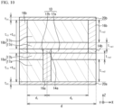
- FIG. 10 is an enlarged cross-sectional view of a thermoelectric conversion device in a first variation of the first embodiment.
- the thermoelectric layers 12a and 12b have different lengths in the X direction.
- the distance between the end of the thermally conductive layer 16b at the thermoelectric layer 12b side and the center of the thermally conductive layer 16a in the X direction is represented by d 1
- d 2 The distance between the end of the thermally conductive layer 16b at the thermoelectric layer 12a side and the center of the thermally conductive layer 16b in the X direction.
- the pitch in the X direction is represented by d.
- t ins1 is preferably d 2 /4 or greater, more preferably d 2 /3 or greater, and further preferably d 2 /2 or greater. Further, t ins1 is preferably 2 ⁇ d 2 or less, more preferably 1.5 ⁇ d 2 or less, and further preferably d 2 or less.
- the distances d 1 and d 2 may be the same to the extent of the manufacturing error, or as in the first variation of the first embodiment, the distances d 1 and d 2 may be different to the extent of the manufacturing error or greater.
- the insulating layers 18a and 18b whose cross sections are illustrated in FIG. 10 are repeatedly arranged at the pitch d in the X direction. Since the pitch d is a constant value, there are two distances d 1 and d 2 . Note that the pitch d may not be necessarily constant. In this case, the largest distance of a plurality of the distances d1 and a plurality of the distances d2 can be used as the reference.
- the second insulating layer that is penetrated by the first thermally conductive layer has a smaller thermal conductivity than the first insulating layer, is provided between the first insulating layer and the first thermoelectric layer and the second thermoelectric layer, and has a thickness equal to or greater than 1/4 of the larger distance of the distance between the end of the first thermally conductive layer at a side of the first thermoelectric layer and the center of the second connection layer in the first direction and the distance between the end of the first thermally conductive layer at a side of the second thermoelectric layer and the center of the second connection layer in the first direction is used as the insulating layers 17b and 17d to which a porous substance of the insulators illustrated in FIG. 2 or FIG. 10 is adopted.
- the space 15 i.e., an air gap
- the base portion 22a, the thermoelectric layers 12a and 12b, and the base portion 22b are produced by a micro-stacking process such as a semiconductor-forming process.
- a thermoelectric conversion device having a very high density and a small size can be provided at a low manufacturing cost, and the strength of the thermoelectric conversion device can be increased.
- the simulation results of FIG. 8A to FIG. 8C can be applied. That is, by adjusting each of the thicknesses of the insulating layers 17b and 17d having low thermal conductivity to be equal to or greater than 1/4 of t C1 , the output power P out can be increased as compared with the case where all of the insulating layers 18a and 18b are made of a material having a low thermal conductivity.
- the output power can be increased to, for example, 75% or greater as compared with the case where all of the insulating layers 18a and 18b are made of HSQ or SiO 2 .
- the mechanical strength of the thermoelectric conversion device can be increased as compared with the case where all of the insulating layers 18a and 18b are made of a material having a low mechanical strength such as porous silica. As described above, it is possible to reduce a decrease in the output power P ou while ensuring the mechanical strength of the thermoelectric conversion device.
- the thermal conductivities of the insulating layers 17b and 17d are 1/8.4 times and 1/25.2 times the thermal conductivities of the insulating layers 17a and 17c (HSQ and SiO 2 ), respectively. Further, the thermal conductivities of the insulating layers 17b and 17d (porous silica) are 1/10800 times the thermal conductivities of the connection layers 14a and 14b and the thermally conductive layers 16a and 16b (Cu).
- the respective ranges of the thermal conductivities of the insulating layers 17b and 17d are preferably equal to or less than 1/5 times and equal to or greater than 1/100 times the thermal conductivities of the insulating layers 17a and 17c.
- the thermal conductivities of the insulating layers 17b and 17d can be equal to or greater than 1/100 times the thermal conductivities of the insulating layers 17a and 17c. This allows the mechanical strength of the thermoelectric conversion device to be ensured while the heat flow through the insulating layers 17b and 17d is reduced to substantially the same range as that of the simulation results described above.
- the respective ranges of the thermal conductivities of the insulating layers 17b and 17d are preferably equal to or less than 1/300 times and equal to or greater than 1/30000 times the thermal conductivities of the connection layers 14a and 14b and the thermally conductive layers 16a and 16b.
- each of the thicknesses of the insulating layers 17b and 17d is preferably adjusted to be equal to or greater than 1/4 times and equal to or less than 2 times tci.
- the thermal conductivities of the insulating layers 17b and 17d are more preferably equal to or less than 1/10 times, further preferably equal to or less than 1/20 times the thermal conductivities of the insulating layers 17a and 17c.
- the thermal conductivities of the insulating layers 17b and 17d are more preferably equal to or less than 1/1000 times, further preferably equal to or less than 1/5000 times the thermal conductivities of the connection layers 14a and 14b and the thermally conductive layers 16a and 16b.
- thermoelectric layers 12a and 12b are low, temperature distribution occurs in the thermoelectric layers 12a and 12b in the comparative example 1. Therefore, the heat flow flowing from the insulating layer 18a into the thermoelectric layers 12a and 12b, such as the heat flow 53 in FIG. 4 , and the heat flow flowing out from the thermoelectric layers 12a and 12b to the insulating layer 18b, such as the heat flow 58 in FIG. 6 , increase.
- the thermal conductivities of the thermoelectric layers 12a and 12b (BiTe) are 1/270 times the thermal conductivities of the connection layers 14a and 14b and the thermally conductive layers 16a and 16b (Cu).
- the thermal conductivities of the thermoelectric layers 12a and 12b are preferably equal to or less than 1/ 50 times the thermal conductivities of the connection layers 14a and 14b and the thermally conductive layers 16a and 16b.
- the thermal conductivities of the thermoelectric layers 12a and 12b are more preferably equal to or less than 1/100 times the thermal conductivities of the connection layers 14a and 14b and the thermally conductive layers 16a and 16b.
- the thermal conductivities of the thermoelectric layers 12a and 12b are, for example, equal to or greater than 1/1000 times the thermal conductivities of the connection layers 14a and 14b and the thermally conductive layers 16a and 16b.
- thermoelectric layers 12a and 12b are too low, the heat flow flowing in the thermoelectric layers 12a and 12b decreases.
- the thermal conductivities of the thermoelectric layers 12a and 12b (BiTe) are 40 times the thermal conductivities of the insulating layers 17b and 17d (porous silica). Therefore, in order to obtain the same effect as the simulation of FIG. 8A to FIG. 8C , the thermal conductivities of the thermoelectric layers 12a and 12b are preferably larger than the thermal conductivities of the insulating layers 17b and 17d.
- the thermal conductivities of the thermoelectric layers 12a and 12b are more preferably equal to or greater than 10 times the thermal conductivities of the insulating layers 17b and 17d.
- the thermal conductivities of the thermoelectric layers 12a and 12b are, for example, equal to or less than 100 times the thermal conductivities of the insulating layers 17b and 17d.
Landscapes
- Cooling Or The Like Of Semiconductors Or Solid State Devices (AREA)
- Measuring Temperature Or Quantity Of Heat (AREA)
Abstract
Description
- The present invention relates to a thermoelectric conversion device.
- There is known a transverse-type µTEG (µTEG: Micro Thermoelectric Generator) in which thermoelectric layers made of a thermoelectric material and connection layers for connecting the thermoelectric layers are alternately arranged in a planar direction, and heat is drawn from the connection layers through a thermally conductive layer in a direction orthogonal to the planar surface (for example, Patent Document 1). The transverse-type µTEG can be applied to thermoelectric power generation using a body temperature with a small temperature difference. It is known to embed an extraction electrode in multilayered insulating layers (a base substrate and a heat insulating substrate) having different thermal conductivities (for example, Patent Document 2).
-
- Patent Document 1: International Publication No.
2018/042708 - Patent Document 2:
Japanese Patent Application Laid-Open No. 2009-158760 - In
FIG. 8 ofPatent Document 2, thermally-insulating substrates (A2, B2) having high thermal insulating properties are disposed on a side provided with thermoelectric materials (5a to 5h, 6a to 6h) of base substrates (A1, B1). In general, the scale in the planar direction and the scale in the height direction are different from each other in the cross-sectional view of the patents, andPatent Document 2 does not describe the thicknesses of the thermally-insulating substrates (A2, B2). In paragraph 0057 ofPatent Document 2, the problem is that the heat flow circumnavigates the thermoelectric materials (5a to 5h, 6a to 6h) between heat-dissipating electrodes (3a to 3i) and heat-absorbing electrodes (2a to 2h, 9a to 8i), which are arranged in the planar direction. When the heat flow in the planar direction is a problem, it is considered that the circumnavigation of the heat flow in the planar direction can be inhibited even if the thermally-insulating substrates (A2, B2) are thin. However, the heat flow circumnavigating the thermoelectric materials (5a to 5h, 6a to 6h) cannot be reduced by simply taking the heat flow in the planar direction into consideration, which results in decrease in the output power of the thermoelectric conversion device. - The present invention has been made in view of the above problems, and an object thereof is to provide a thermoelectric conversion device having large output power.
- The present invention is a thermoelectric conversion device including: first thermoelectric layers and second thermoelectric layers that are alternately provided in a first direction parallel to surfaces of the first thermoelectric layers and the second thermoelectric layers, the first thermoelectric layers having conductivity types opposite to those of the second thermoelectric layers; first connection layers and second connection layers that are electrically and thermally connected to the first thermoelectric layers and the second thermoelectric layers between the first thermoelectric layers and the second thermoelectric layers, the first connection layers and the second connection layers being alternately provided in the first direction; first thermally conductive layers that are thermally connected to the first connection layers, the first thermally conductive layers extending in a second direction intersecting the surfaces; a first insulating layer through which the first thermally conductive layers penetrate, the first insulating layer having a thermal conductivity smaller than thermal conductivities of the first thermally conductive layers; a second insulating layer through which the first thermally conductive layers penetrate, the second insulating layer having a thermal conductivity smaller than the thermal conductivity of the first insulating layer, the second insulating layer being provided between the first insulating layer and the first thermoelectric layers and the second thermoelectric layers, the second insulating layer having a thickness equal to or greater than 1/4 of a larger distance of a distance between an end of the first thermally conductive layer at a side of the first thermoelectric layer and a center of the second connection layer in the first direction and a distance between an end of the first thermally conductive layer at a side of the second thermoelectric layer and the center of the second connection layer in the first direction.
- In the above configuration, a configuration in which provided are: second thermally conductive layers that are thermally connected to the second connection layers, the second thermally conductive layers being provided at a side opposite to the first thermally conductive layers with respect to the first thermoelectric layers and the second thermoelectric layers, the second thermally conductive layers extending in the second direction; a third insulating layer through which the second thermally conductive layers penetrate, the third insulating layer having a thermal conductivity smaller than thermal conductivities of the second thermally conductive layers; and a fourth insulating layer through which the second thermally conductive layers penetrate, the fourth insulating layer having a thermal conductivity smaller than the thermal conductivity of the third insulating layer, the fourth insulating layer being provided between the third insulating layer and the first thermoelectric layers and the second thermoelectric layers, the fourth insulating layer having a thickness equal to or greater than 1/4 of the larger distance may be employed.
- In the above configuration, a configuration in which the thickness of the second insulating layer is equal to or less than twice the larger distance may be employed.
- In the above configuration, a configuration in which a thickness of the first insulating layer is equal to or greater than 1/2 of the thickness of the second insulating layer may be employed.
- In the above configuration, a configuration in which the second insulating layer is porous, and the first insulating layer is non-porous may be employed.
- In the above configuration, a configuration in which the second insulating layer is in contact with the first thermoelectric layers and the second thermoelectric layers, and is in contact with the first insulating layer may be employed.
- In the above configuration, a configuration in which the fourth insulating layer is porous, and the third insulating layer is non-porous may be employed.
- In the above configuration, a configuration in which the fourth insulating layer is in contact with the first thermoelectric layers and the second thermoelectric layers, and is in contact with the third insulating layer may be employed.
- In the above configuration, a configuration in which the second insulating layer is in contact with the first thermoelectric layers and the second thermoelectric layers, and is in contact with the first insulating layer, the thickness of the second insulating layer is equal to or less than twice the larger distance, and the thickness of the fourth insulating layer is equal to or less than twice the larger distance may be employed.
- In the above configuration, a configuration in which the thermal conductivity of the second insulating layer and the thermal conductivity of the fourth insulating layer are equal to or less than 1/5 times and equal to or greater than 1/100 times a thermal conductivity of the first insulating layer and a thermal conductivity of the second insulating layer may be employed.
- In the above configuration, a configuration in which the thermal conductivity of the second insulating layer and the thermal conductivity of the fourth insulating layer are equal to or less than 1/300 times and equal to or greater than 1/30000 times the thermal conductivities of the first connection layer, the second connection layer, the first thermally conductive layer, and the second thermally conductive layer may be employed.
- In the above configuration, a configuration in which the thermal conductivities of the first thermoelectric layers and the second thermoelectric layers are equal to or less than 1/50 times the thermal conductivities of the first connection layers, the second connection layers, the first thermally conductive layers, and the second thermally conductive layers may be provided.
- In the above configuration, a configuration in which the thermal conductivities of the first thermoelectric layers and the second thermoelectric layer are greater than the thermal conductivities of the second insulating layer and the fourth insulating layer may be employed.
- In the above configuration, a configuration in which the first insulating layer and the third insulating layer are HSQ layers or silicon oxide layers, and the second insulating layer and the fourth insulating layer are porous silica may be employed.
- In the above configuration, a configuration in which the distance between the end of the first thermally conductive layer at the side of the first thermoelectric layer and the center of the second connection layer in the first direction is the same as the distance between the end of the first thermally conductive layer at the side of the second thermoelectric layer and the center of the second connection layer in the first direction may be employed.
- The present invention can provide a thermoelectric conversion device having large output power.
-
-
FIG. 1A is a plan view of a thermoelectric conversion device in accordance with a first embodiment, andFIG. 1B is a cross-sectional view taken along line A-A inFIG. 1A ; -
FIG. 2 is an enlarged cross-sectional view of the thermoelectric conversion device in accordance with the first embodiment; -
FIG. 3A is a plan view of a thermoelectric conversion module in accordance with the first embodiment, andFIG. 3B is a cross-sectional view taken along line A-A inFIG. 3A ; -
FIG. 4 illustrates heat flow in a comparative example 1; -
FIG. 5A and FIG. 5B are graphs presenting normalized heat flow versus normalized X and normalized Z, respectively; -
FIG. 6 illustrates heat flow in the comparative example 1; -
FIG. 7A and FIG. 7B are graphs presenting normalized heat flow versus normalized X and normalized Z, respectively; -
FIG. 8A to FIG. 8C are graphs presenting Pout versus tins1 in the first embodiment; -
FIG. 9A to FIG. 9E are graphs presenting current I and output power Pout versus output voltage Vout in respective samples; and -
FIG. 10 is an enlarged cross-sectional view of a thermoelectric conversion device in accordance with a first variation of the first embodiment. -
FIG. 8 ofPatent Document 2 does not describe the thicknesses of the thermally-insulating substrates (A2, B2) as described above. If the thermally-insulating substrates (A2, B2) having a low mechanical strength are thick, the mechanical strength of the thermoelectric conversion device is low. If the thermally insulating substrates (A2, B2) are thin, the thermoelectric conversion device is deteriorated in performances. In addition, inFIG. 8 ofPatent Document 2, spaces 15 (that is, air gaps) are provided between the thermoelectric materials (5a to 5h, 6a to 6h) and the thermally-insulating substrate (B2). Air gaps provided between the thermoelectric material and the thermally-insulating substrate reduce the strength of the thermoelectric conversion device. - Therefore, a thermoelectric conversion device having no air gap was simulated by using a highly accurate distributed constant circuit model developed by the inventors. The distributed constant circuit model allows for highly accurate simulations by taking into account the thermal conductivity of each material. The simulation results has revealed, for the first time, a structure that can reduce degradation in performances such as output power while ensuring mechanical strength. Embodiments and simulation results thereof will be described below.
-
FIG. 1A is a plan view of a thermoelectric conversion device in a first embodiment, andFIG. 1B is a cross-sectional view taken along line A-A inFIG. 1A .FIG. 2 is an enlarged cross-sectional view of the thermoelectric conversion device in the first embodiment. InFIG. 1A , thermoelectric layers, connection layers, and electrodes are illustrated. The surfaces ofthermoelectric layers thermoelectric layers - As illustrated in
FIG. 1A, FIG. 1B , andFIG. 2 , in athermoelectric conversion device 30, thethermoelectric layer 12a (a first thermoelectric layer) and thethermoelectric layer 12b (a second thermoelectric layer) have a strip shape extending in the Y direction. Thethermoelectric layers thermoelectric layers thermoelectric layers connection layers 14a (a first connection layer) and 14b (a second connection layer) in the X-direction. The connection layers 14a and 14b extend in the Y direction. A pair of thethermoelectric layers Seebeck element 10. A plurality of theSeebeck elements 10 are connected in series betweenelectrodes - The connection layers 14a and 14b are thermally connected to thermally
conductive layers 16a (a first thermally conductive layer) and 16b (a second thermally conductive layer) in the -Z direction and the +Z direction (a second direction intersecting the surface), respectively. The thermallyconductive layers base portions films conductive layers layers layer 18a includes insulatinglayers 17a (a first insulating layer) and 17b (a second insulating layer). The insulatinglayer 17b is provided between the insulatinglayer 17a and theSeebeck element 10 and between the insulatinglayer 17a and the connection layers 14a and 14b. The insulatinglayer 18b includes insulatinglayers 17c (a third insulating layer) and 17d (a fourth insulating layer). The insulatinglayer 17d is provided between the insulatinglayer 17c and theSeebeck element 10 and between the insulatinglayer 17c and the connection layers 14a and 14b. The insulatinglayers thermoelectric layers conductive layers layers layers films conductive layers layers conductive layers layers layers -
FIG. 3A is a plan view of a thermoelectric conversion module in the first embodiment, andFIG. 3B is a cross-sectional view taken along line A-A inFIG. 3A . As illustrated inFIG. 3A and FIG. 3B , in athermoelectric conversion module 100, thebase portions heat sink 33 is thermally connected to the upper surface of thebase portion 22b. A surface of thebase portion 22a facing thebase portion 22b has a protruding portion. Thebase portion 22a has asection 35, which protrudes toward thebase portion 22b, andsections 36, which do not protrude. The distance H between thebase portions section 36 is greater than the distance between thebase portions section 35. For example, thebase portion 22b has a flat plate shape, and thebase portion 22a has a shape in which a protruding portion is provided on a flat plate. The protruding portion may be provided on the lower surface of thebase portion 22b, or the protruding portions may be provided on both the upper surface of thebase portion 22a and the lower surface of thebase portion 22b. Although the planar shapes of thebase portions section 35 are illustrated as squares as an example, these planar shapes can be freely selected. - A
support 34 is provided between thebase portions base portions thermal insulator 32 is provided between thebase portions support 34. Thethermal insulator 32 is, for example, a gas having a pressure lower than atmospheric pressure or a vacuum. Thesupport 34 maintains the pressure or vacuum of thethermal insulator 32. Thesupport 34 mechanically supports thebase portion 22a and thebase portion 22b. The thermal conductivity of thethermal insulator 32 is smaller than the thermal conductivities of thethermoelectric conversion device 30, thebase portions support 34. - The
thermoelectric conversion device 30 includes a plurality ofblocks 31a to 31c. In each of theblocks 31a to 31c, a plurality of thethermoelectric layers blocks 31a to 31c are arranged in the Y direction. Anelectrode 24c connects theblocks electrode 24d connects theblocks Seebeck elements 10 are connected in series between theelectrodes thermoelectric conversion device 30 are the same as those illustrated inFIG. 1A to FIG. 2 , and description thereof will be omitted. - In applications where the operating temperature is near room temperature or up to about several hundred degrees Celsius, the thermoelectric materials used for the
thermoelectric layers thermoelectric layers thermoelectric layers - The
thermoelectric layers thermoelectric layers thermoelectric layers thermoelectric layers - The connection layers 14a and 14b are preferably made of a material having a high electric conductivity and a high thermal conductivity. For example, metal layers of Cu, Al, Au, or Ag can be used. The connection layers 14a and 14b may be made of different materials.
- As the insulating
layers layers layers - The
base portions films films base portions base portions films base portions base portions base portions base portions base portion base portions - The
support 34 preferably has a low thermal conductivity, and is preferably made of a material harder than thethermal insulator 32 to support thebase portions support 34, for example, a polymer organic material such as resin or rubber can be used. For example, in the case that thethermal insulator 32 is solid, the yield strength of thesupport 34 is preferably higher than that of thethermal insulator 32 to reinforce thethermal insulator 32. - First, simulation was performed on a comparative example 1 in which the insulating
layers layers layers - The structural parameters illustrated in
FIG. 1 to FIG. 3 were defined as follows. - D: Widths of the
base portions - D': Widths of the
section 35 in the X direction and the Y direction - D0: Length of the thermoelectric conversion device 30 (total length of the
blocks 31a to 31c) in the X-direction - H: Distance between the
base portions section 36 - x: Widths of the
support 34 in the X direction and the Y direction - d: Pitch of the
thermoelectric layers - γ: Trade-off parameter, which is the parameter with which the width occupied by the
thermoelectric layers - yd: Widths of the
thermoelectric layers - (1 - γ)d: Distance between the
thermoelectric layers - L: Lengths of the
thermoelectric layers - ts: Thicknesses of the
thermoelectric layers - tin1: Thicknesses of the insulating
layers - tin2: Thicknesses of the insulating
layers - tc= tC1+ tC2: Thicknesses of the insulating
layers - tci: Larger one of the distance between the end of the thermally
conductive layer 16a and the center of the thermallyconductive layer 16b in the X direction and the distance between the end of the thermallyconductive layer 16b and the center of the thermallyconductive layer 16a in the X direction - tPI: Thicknesses of the insulating
films - m0: Number of pairs of the
thermoelectric layers - ΔTS: Temperature difference between the lower surface of the
base portion 22a and the upper surface of thebase portion 22b - Pout: Output power of the thermoelectric conversion device
- In the case that the
thermoelectric conversion module 100 is used as a power source of a wearable device, thethermoelectric conversion module 100 generates electric power using a temperature difference between the body temperature of the human body and the temperature of the atmosphere. Therefore, a homeothermic animal model was used for human body temperature. The details of the simulation are described in IEEE Transactions on Electron Devices, doi: 10.1109/TED.2020.3006168. In the simulation, γ, yd, (1 - γ)d, m0, L, and tci are optimized so that the power Pout is maximized. As a model in thethermoelectric conversion device 30, a highly accurate distributed constant circuit model was used. - The simulation conditions for each dimension and material were as follows.


- D0 = 9 mm
- H = 5 mm
- x = 0.5 mm
- ts= 1000 nm
- tPI= 100 nm
-
- Material: BiTe
- Seebeck coefficient = Sp - Sn: 434 µV/K
- Thermal conductivity λ = (λp + λn)/2: 1. 43 W/(m·K)
- Electrical resistivity ρ = (ρp + ρn)/2: 8.11 µΩ·m
- Note that λn and ρn are the thermal conductivity and electrical resistivity of the
thermoelectric layer 12a, respectively, and λp and ρp are the thermal conductivity and electrical resistivity of thethermoelectric layer 12b, respectively. - Connection layers 14a, 14b, thermally
conductive layers - Material: Cu
- Thermal conductivity λC: 386 W/(m K)
- Electric resistivity ρC: 17 nΩ·m
- Insulating
films - Material: AlOx
- Thermal conductivity λPI: 1.5 W/(m·K)
-
Support 34- Material: Organic material
- Thermal conductivity λWL: 0.15 W/(m·K)
-
Thermal insulator 32
Vacuum - Contact resistance
- BiTe and Cu
- Electrical contact-resistance rPC: 1.0 Ω·µm2
- Thermal contact-resistance kPC: 140 µm2·K/mW
- Cu and AlOx
Thermal contact-resistance kC-PI: 3.4 µm2·K/mW
- BiTe and Cu
- The temperature difference between the body temperature of the human body and the temperature of the atmosphere was set as 10 K. The electrical contact-resistance is an electrical resistance per unit area on a surface where two materials are in contact with each other, and the thermal contact-resistance is a thermal resistance per unit area on a surface where two materials are in contact with each other.
- The simulation was performed for the following three materials as the insulating
layers - Sample PS
- Material: Porous silica
- Thermal conductivity λPS: 35.7 mW/(m·K)
- Sample HSQ
- Material: Hydrogen silsesquioxane
- Thermal conductivity λHSQ: 0.3 W/(m·K)
- Sample SiO2
- Material: SiO2
- Thermal conductivity λSiO2: 0.9 W/(m·K)
- PS has a low thermal conductivity but is brittle. Therefore, it is difficult to form a thick layer. SiO2 has high mechanical strength and can be easily formed thick, but has high thermal conductivity. HSQ (hydrogen silsesquioxane) is a molecule formed by doping silsesquioxane, which is an intermediate material between silica and silicon, with hydrogen, and has a less mechanical strength than SiO2 but has a lower thermal conductivity than SiO2.
- Table 1 is not related to tC2 + tci presented in
FIG. 2 , and is a table presenting optimized output power Pout and each parameter in the case where each of the insulatinglayers [Table 1] Sample PS HSQ SiO2 Pout [µW] 16.15 7.055 3.014 γd [µm] 7.92 3.21 2.06 (1-γ)d [µm] 2.93 2.06 2.15 m0 [pairs] 415 854 1069 L [µm] 7.18 1.25 0.525 tC1 [µm] 9.38 4.24 3.14 - As presented in Table 1, although the output power Pout of the sample PS is 16.15 µW, the output power Pout of the sample HSQ is equal to or less than 1/2 of that of the sample PS, and the output power Pout of the sample SiO2 is equal to or less than 1/5 of that of the sample PS. Since the thermal conductivities of the insulating
layers - In the comparative example 1, when PS is used as the insulating
layers layers - The leakage of heat flow from the
thermoelectric layers conductive layers layers -
FIG. 4 illustrates heat flow in the comparative example 1. The lower surface of the insulatingfilm 20a was set to a high temperature, and the upper surface of the insulatingfilm 20b was set to a low temperature.Heat flow 54 leaking from the thermallyconductive layer 16a to the insulatinglayer 18a andheat flow 53 flowing from the insulatinglayer 18a into each of thethermoelectric layers thermoelectric layers thermoelectric layers connection layer 14b was defined as 0, and the position X at which thethermoelectric layers connection layer 14a was defined as 1. The position Z of the Z coordinate of the thermallyconductive layer 16a was normalized. The position Z at which the thermallyconductive layer 16a and the insulatingfilm 20a were in contact with each other was defined as 0, and the position Z at which the thermallyconductive layer 16a and theconnection layer 14a were in contact with each other was defined as 1. -
FIG. 5A and FIG. 5B are graphs presenting normalized heat flow versus normalized X and normalized Z, respectively. In the simulation, the range of 0 to 1 of the normalized X and the range of 0 to 1 of the normalized Z were divided into 10 ranges and 15 ranges, respectively. Dots inFIG. 5A and FIG. 5B indicate the sum of the normalized heat flows in the respective divided ranges. A straight line is a line connecting dots.FIG. 5A presents the normalizedheat flow 53 flowing from the insulatinglayer 18a into thethermoelectric layers film 20a from the outside. As presented inFIG. 5A , for the sample HSQ, in aregion 51, the normalizedheat flow 53 is large around the normalized x = 0, and the normalizedheat flow 53 decreases as the normalized x increases. This means that as the normalized X increases, the temperatures of thethermoelectric layers thermoelectric layers layer 18a increases. In aregion 50, the normalizedheat flow 53 increases as the normalized X increases. -
FIG. 5B presents the normalizedheat flow 54 leaking from the thermallyconductive layer 16a to the insulatinglayer 18a. As presented inFIG. 5B , for the sample HSQ, the normalizedheat flow 54 is substantially zero in aregion 52. In theregion 50, the normalizedheat flow 54 increases as the normalized Z increases. As is clear from above, it has been revealed that in theregion 50 ofFIG. 4 , there is a heat flow from the thermallyconductive layer 16a to thethermoelectric layers layer 18a. This may be considered because the heat flow that is less likely to flow from theconnection layer 14a to thethermoelectric layers conductive layer 16a and thethermoelectric layers region 50. However, since the thermal contact-resistance kpc is sufficiently small, it is considered that the heat flow through theregion 50 is due to the high thermal conductivity of the insulatinglayer 18a. In the sample PS, the normalized heat flows 53 and 54 inFIG. 5A and FIG. 5B are smaller than those in the sample HSQ. This is considered because, in the sample PS, the thermal conductivity of the insulatinglayer 18a is small and thus heat passing through the insulatinglayer 18a is small. -
FIG. 6 illustrates heat flow in the comparative example 1. The lower surface of the insulatingfilm 20a was set to a high temperature, and the upper surface of the insulatingfilm 20b was set to a low temperature.Heat flow 58 leaking from each of thethermoelectric layers layer 18b andheat flow 59 flowing from the insulatinglayer 18b to the thermallyconductive layer 16b were simulated. The normalized X is the same as inFIG. 4 . The position Z at which the thermallyconductive layer 16b and theconnection layer 14b were in contact with each other was defined as 0, and the position Z at which the thermallyconductive layer 16b and the insulatingfilm 20b were in contact with each other was defined as 1. -
FIG. 7A and FIG. 7B are graphs presenting normalized heat flow versus normalized X and normalized Z, respectively.FIG. 7A presents the normalizedheat flow 58 flowing from thethermoelectric layers layer 18b. As presented inFIG. 7A , for the sample HSQ, in aregion 56, the normalizedheat flow 58 is large around the normalized X = 1, and the normalizedheat flow 58 decreases as the normalized X decreases. This is due to the temperature distribution in thethermoelectric layers region 55, the normalizedheat flow 58 increases as the normalized X decreases. -
FIG. 7B presents the normalizedheat flow 59 flowing from the insulatinglayer 18b into the thermallyconductive layer 16b. As presented inFIG. 7B , in the sample HSQ, the normalizedheat flow 59 is substantially zero in aregion 57. In theregion 55, the normalizedheat flow 59 increases as the normalized Z decreases. As described above, it has been revealed that in theregion 55 ofFIG. 6 , there is heat flow from thethermoelectric layers conductive layer 16b through the insulatinglayer 18b. It is considered that the heat flow through theregion 55 is due to the high thermal conductivity of the insulatinglayer 18b. Also inFIG. 7A and FIG. 7B , the normalized heat flows 58 and 59 of the sample PS are smaller than those of the sample HSQ. This is considered because, in the sample PS, the thermal conductivity of the insulatinglayer 18b is small, and thus the heat flow passing through the insulatinglayer 18b is small. - As described above, the heat flow passing through the insulating
layers thermoelectric layers regions layers Patent Document 2. It is considered that the output power Pout is lower in the samples HSQ and SiO2 than in the sample PS because of the leakage of the heat flow to the insulatinglayers - The sample HSQ/PS is a sample adopting HSQ as the insulating
layers layers layers layers layers -
FIG. 8A to FIG. 8C are graphs presenting Pout versus tins1 in the first embodiment. The samples HSQ/PS and SiO2/PS are presented as the first embodiment, and the sample PS is presented as the comparative example 1. In the sample PS, tins1 = tC1 + tC2, but for comparison with the samples HSQ/PS and SiO2/PS, Pout is illustrated by a dotted straight line that takes a constant value regardless of the value of tins1. As presented inFIG. 8A to FIG. 8C , the output power Pout of both samples HSQ/PS and SiO2/PS is less than or equal to 1/2 of that of the sample PS around tins1 = 0. As tins1 increases, the output power Pout approaches that of the sample PS, and at tins1= tC1, the output power Pout of the samples HSQ/PS and SiO2/PS is almost the same as the output power Pout of the sample PS. - Table 2 is a table presenting the ratio PoutHSQ/PoutPS indicating the output voltage PoutHSQ of the sample HSQ/PS with respect to the output voltage PoutPS of the sample PS.
[Table 2] PoutHSQ/PoutPS tins1 = tC1 tins1 = tC1/2 tC2 = 1 µm 0.996 0.935 tC2 = 10 µm 0.988 0.920 tC2 = 30 µm 0.984 0.909 - Table 3 is a table presenting the ratio PoutSiO2/PoutPS indicating the output voltage PoutSiO2 of the sample SiO2/PS with respect to the output voltage PoutPS of the sample PS.
[Table 3] PoutSiO2/PoutPS tins1 = tC1 tins1 = tC1/2 tC2 = 1 µm 0.999 0.927 tC2 = 10 µm 0.988 0.906 tC2 = 30 µm 0.983 0.893 - Table 2 and Table 3 present PoutHSQ/PoutPS and PoutSiO2/PoutPS when tC2 is 1 µm, 10 µm, or 30 µm, and tins1 is tci or tC/2. As presented in Table 2 and Table 3, when tins1= tci, PoutHSQ and PoutSiO2 are substantially the same as PoutPS regardless of tC2. When tins1= tC1/2, PoutHSQ and PoutSiO2 are approximately 90% of PoutPS regardless of tC2. As presented in
FIG. 8A to FIG. 8C , when tins1= tC1/4, PoutHSQ and PoutSiO2 are approximately 75% of PoutPS, and when tins1= tC1/3, PoutHSQ and PoutSiO2 are approximately 85% of PoutPS. As described above, the output power Pout cannot be increased unless the thicknesses tins1 of the insulatinglayers - The reasons why the output power Pout cannot be increased unless the thicknesses tins1 of the insulating
layers FIG. 4 , theheat flow 53 flowing from the insulatinglayer 18a into thethermoelectric layers thermoelectric layers layer 18a. Further, theregion 50 in which theheat flow 54 leaking from the thermallyconductive layer 16a to the insulatinglayer 18a is present extends to the section from thethermoelectric layers FIG. 6 , theheat flow 58 leaking from thethermoelectric layers layer 18b around the normalized X = 1 passes through the section from thethermoelectric layers layer 18b. Further, theregion 55 in which theheat flow 59 flowing from the insulatinglayer 18b into the thermallyconductive layer 16b is present extends to the section from thethermoelectric layers - Such a behavior of the output power Pout with respect to the thicknesses tins1 of the insulating
layers Patent Document 2, and is a finding obtained by starting simulation of the highly accurate distributed constant circuit model as presented inFIG. 4 to FIG. 7B . - In the first embodiment, the thicknesses tins1 of the insulating
layers conductive layer 16a at thethermoelectric layer 12a side and the center of the thermallyconductive layer 16b in the X direction and the distance between the end of the thermallyconductive layer 16a at thethermoelectric layer 12b side and the center of the thermallyconductive layer 16b in the X direction. The thickness tins1 is more preferably tci/3 or greater, further preferablyt C12 or greater. This is because the simulation of the highly accurate distributed constant circuit model has revealed that the output power of about 90% of the output power of the sample PS is obtained by adjusting the thicknesses tinti of the insulatinglayers - Even if the thickness tins1 becomes thicker than tci, the output power Pout does not increase. Therefore, in order to increase the mechanical strength of the insulating
layers layers FIG. 8A to FIG. 8C . Further, the thickness tins1 of either one of the insulatinglayers - In order to increase the mechanical strength of the insulating
layers layers - The thermal conductivities of the insulating
layers conductive layers layers conductive layers layers layers layers layers layers layers layers layers layers layers layers layers layers - Table 4 is a table presenting the percentage of increase of the output power Pout of the sample HSQ/PS with respect to that of the sample HSQ and the percentage of increase the output power Pout of the sample SiO2/PS with respect to that of the sample SiO2. Note that tC2 = 30 µm and tinsi = tci.
[Table 4] TC2= 30 µm, Tins1 = TC1. Percentage of increase of Pout of HSQ/PS with respect to HSQ 125% Percentage of increase of Pout of SiO2/PS with respect to SiO2 426% - As presented in Table 4, the sample HSQ/PS has Pout increased by 125% compared to the sample HSQ, and the sample SiO2/PS has Pout increased by 426% compared to the sample SiO2.
-
FIG. 9A to FIG. 9E are graphs presenting the current I and the output power Pout versus the output voltage Vout in each sample.FIG. 9A presents the sample PS,FIG. 9B presents the sample HSQ,FIG. 9C presents the sample SiO2,FIG. 9D presents the sample HSQ/PS, andFIG. 9E presents the sample SiO2/PS. A plurality of modules in which the areas of thebase portions - As presented in
FIG. 9A to FIG. 9E , when the output voltage Vout is substantially 1 V, the power Pout peaks. As presented inFIG. 9A , in the sample PS, when the mounting area SA is 120 cm2, an output power Pout of about 2 mW is achieved. However, in the sample PS, the mechanical strength of the insulatinglayers FIG. 9B and FIG. 9C , in the samples HSQ and SiO2, although the mechanical strength of the insulatinglayers FIG. 9D and FIG. 9E , in the samples HSQ/PS and SiO2/PS, when SA is 120 cm2, the output power Pout is about 2 mW, which is almost the same as that of the sample PS. Since the insulatinglayers -
FIG. 10 is an enlarged cross-sectional view of a thermoelectric conversion device in a first variation of the first embodiment. As illustrated inFIG. 10 , in the first variation of the first embodiment, thethermoelectric layers conductive layer 16b at thethermoelectric layer 12b side and the center of the thermallyconductive layer 16a in the X direction is represented by d1, and the distance between the end of the thermallyconductive layer 16b at thethermoelectric layer 12a side and the center of the thermallyconductive layer 16b in the X direction is represented by d2. The pitch in the X direction is represented by d. - In the case that the distances diand d2 are different from each other as in the first variation of the first embodiment, it is required to reduce both the heat flow bypassing the insulating
layer 18a and the heat flow bypassing the insulatinglayer 18b. Therefore, the larger distance d2 of the distances d1 and d2 is used as the reference. That is, tins1 is preferably d2/4 or greater, more preferably d2/3 or greater, and further preferably d2/2 or greater. Further, tins1 is preferably 2 × d2 or less, more preferably 1.5 × d2 or less, and further preferably d2 or less. As in the first embodiment, the distances d1 and d2 may be the same to the extent of the manufacturing error, or as in the first variation of the first embodiment, the distances d1 and d2 may be different to the extent of the manufacturing error or greater. In the above described embodiment, the insulatinglayers FIG. 10 are repeatedly arranged at the pitch d in the X direction. Since the pitch d is a constant value, there are two distances d1 and d2. Note that the pitch d may not be necessarily constant. In this case, the largest distance of a plurality of the distances d1 and a plurality of the distances d2 can be used as the reference. - In the above-described embodiment, the second insulating layer that is penetrated by the first thermally conductive layer, has a smaller thermal conductivity than the first insulating layer, is provided between the first insulating layer and the first thermoelectric layer and the second thermoelectric layer, and has a thickness equal to or greater than 1/4 of the larger distance of the distance between the end of the first thermally conductive layer at a side of the first thermoelectric layer and the center of the second connection layer in the first direction and the distance between the end of the first thermally conductive layer at a side of the second thermoelectric layer and the center of the second connection layer in the first direction is used as the insulating
layers FIG. 2 orFIG. 10 is adopted. - As illustrated in
FIG. 1A to FIG. 2 , in the case that the insulatinglayer 17b is in contact with thethermoelectric layers layer 17a, and the insulatinglayer 17d is in contact with thethermoelectric layers layer 17a, the space 15 (i.e., an air gap) as illustrated inFIG. 8 ofPatent Document 2 is not formed between thebase portion 22a and thethermoelectric layers base portion 22b and thethermoelectric layers base portion 22a, thethermoelectric layers base portion 22b are produced by a micro-stacking process such as a semiconductor-forming process. As a result, a thermoelectric conversion device having a very high density and a small size can be provided at a low manufacturing cost, and the strength of the thermoelectric conversion device can be increased. - When the thermal conductivities of the insulating
layers layers FIG. 8A to FIG. 8C can be applied. That is, by adjusting each of the thicknesses of the insulatinglayers layers layers layers FIG. 8A to FIG. 8C , the output power can be increased to, for example, 75% or greater as compared with the case where all of the insulatinglayers - Further, as presented in
FIG. 8A to FIG. 8C , even if each of the thicknesses of the insulatinglayers layers layers layers - In the simulations in
FIG. 8A to FIG. 8C , for the samples HSQ/PS and SiO2/PS, the thermal conductivities of the insulatinglayers layers layers conductive layers - In order to obtain the same effect as the simulation results in
FIG. 8A to FIG. 8C , the respective ranges of the thermal conductivities of the insulatinglayers layers layers layers layers layers layers layers layers - The respective ranges of the thermal conductivities of the insulating
layers conductive layers layers conductive layers conductive layers layers layers conductive layers layers layers layers - To obtain the same effect as the simulation results of
FIG. 8A to FIG. 8C , the thermal conductivities of the insulatinglayers layers layers conductive layers - In the case that the thermal conductivities of the
thermoelectric layers thermoelectric layers layer 18a into thethermoelectric layers heat flow 53 inFIG. 4 , and the heat flow flowing out from thethermoelectric layers layer 18b, such as theheat flow 58 inFIG. 6 , increase. In the simulations ofFIG. 8A to FIG. 8C , the thermal conductivities of thethermoelectric layers conductive layers FIG. 8A to FIG. 8C , the thermal conductivities of thethermoelectric layers conductive layers - In order to obtain the same effect as the simulation results of
FIG. 8A to FIG. 8C , the thermal conductivities of thethermoelectric layers conductive layers thermoelectric layers conductive layers - If the thermal conductivities of the
thermoelectric layers thermoelectric layers FIG. 8A to FIG. 8C , the thermal conductivities of thethermoelectric layers layers FIG. 8A to FIG. 8C , the thermal conductivities of thethermoelectric layers layers FIG. 8A to FIG. 8C , the thermal conductivities of thethermoelectric layers layers thermoelectric layers layers - Although preferred embodiments of the present invention have been described so far, the present invention is not limited to those particular embodiments, and various changes and modifications may be made to them within the scope of the invention claimed herein.
-
- 10 Seebeck element
- 12a, 12b thermoelectric layer
- 14a, 14b connection layer
- 16a, 16b thermally conductive layer
- 17a to 17d, 18a, 18b insulating layer
- 22a, 22b base portion
- 24a to 24d electrode
Claims (15)
- A thermoelectric conversion device comprising:first thermoelectric layers and second thermoelectric layers that are alternately provided in a first direction parallel to surfaces of the first thermoelectric layers and the second thermoelectric layers, the first thermoelectric layers having conductivity types opposite to those of the second thermoelectric layers;first connection layers and second connection layers that are electrically and thermally connected to the first thermoelectric layers and the second thermoelectric layers between the first thermoelectric layers and the second thermoelectric layers, the first connection layers and the second connection layers being alternately provided in the first direction;first thermally conductive layers that are thermally connected to the first connection layers, the first thermally conductive layers extending in a second direction intersecting the surfaces;a first insulating layer through which the first thermally conductive layers penetrate, the first insulating layer having a thermal conductivity smaller than thermal conductivities of the first thermally conductive layers;a second insulating layer through which the first thermally conductive layers penetrate, the second insulating layer having a thermal conductivity smaller than the thermal conductivity of the first insulating layer, the second insulating layer being provided between the first insulating layer and the first thermoelectric layers and the second thermoelectric layers, the second insulating layer having a thickness equal to or greater than 1/4 of a larger distance of a distance between an end of the first thermally conductive layer at a side of the first thermoelectric layer and a center of the second connection layer in the first direction and a distance between an end of the first thermally conductive layer at a side of the second thermoelectric layer and the center of the second connection layer in the first direction.
- The thermoelectric conversion device according to claim 1, further comprising:second thermally conductive layers that are thermally connected to the second connection layers, the second thermally conductive layers being provided at a side opposite to the first thermally conductive layers with respect to the first thermoelectric layers and the second thermoelectric layers, the second thermally conductive layers extending in the second direction;a third insulating layer through which the second thermally conductive layers penetrate, the third insulating layer having a thermal conductivity smaller than thermal conductivities of the second thermally conductive layers; anda fourth insulating layer through which the second thermally conductive layers penetrate, the fourth insulating layer having a thermal conductivity smaller than the thermal conductivity of the third insulating layer, the fourth insulating layer being provided between the third insulating layer and the first thermoelectric layers and the second thermoelectric layers, the fourth insulating layer having a thickness equal to or greater than 1/4 of the larger distance.
- The thermoelectric conversion device according to claim 1 or 2, wherein the thickness of the second insulating layer is equal to or less than twice the larger distance.
- The thermoelectric conversion device according to any one of claims 1 to 3, wherein a thickness of the first insulating layer is equal to or greater than 1/2 of the thickness of the second insulating layer.
- The thermoelectric conversion device according to any one of claims 1 to 4, wherein the second insulating layer is porous, and the first insulating layer is non-porous.
- The thermoelectric conversion device according to any one of claims 1 to 5, wherein the second insulating layer is in contact with the first thermoelectric layers and the second thermoelectric layer, and is in contact with the first insulating layer.
- The thermoelectric conversion device according to claim 2, wherein the fourth insulating layer is porous, and the third insulating layer is non-porous.
- The thermoelectric conversion device according to claim 2 or 7, wherein the fourth insulating layer is in contact with the first thermoelectric layers and the second thermoelectric layers, and is in contact with the third insulating layer.
- The thermoelectric conversion device according to claim 8,wherein the second insulating layer is in contact with the first thermoelectric layers and the second thermoelectric layers, and is in contact with the first insulating layer,wherein the thickness of the second insulating layer is equal to or less than twice the larger distance, andwherein the thickness of the fourth insulating layer is equal to or less than twice the larger distance.
- The thermoelectric conversion device according to claim 9, wherein the thermal conductivity of the second insulating layer and the thermal conductivity of the fourth insulating layer are equal to or less than 1/5 times and equal to or greater than 1/100 times the thermal conductivity of the first insulating layer and the thermal conductivity of the second insulating layer.
- The thermoelectric conversion device according to claim 10, wherein the thermal conductivity of the second insulating layer and the thermal conductivity of the fourth insulating layer are equal to or less than 1/300 times and equal to or greater than 1/30000 times the thermal conductivities of the first connection layers, the second connection layers, the first thermally conductive layers, and the second thermally conductive layers.
- The thermoelectric conversion device according to claim 11, wherein the thermal conductivities of the first thermoelectric layers and the second thermoelectric layers are equal to or less than 1/50 times the thermal conductivities of the first connection layers, the second connection layers, the first thermally conductive layers, and the second thermally conductive layers.
- The thermoelectric conversion device according to claim 12, wherein the thermal conductivities of the first thermoelectric layers and the second thermoelectric layers are greater than the thermal conductivities of the second insulating layer and the fourth insulating layer.
- The thermoelectric conversion device according to any one of claims 2 and 7 to 13, wherein the first insulating layer and the third insulating layer are HSQ layers or silicon oxide layers, and the second insulating layer and the fourth insulating layer are porous silica.
- The thermoelectric conversion device according to any one of claims 1 to 14, wherein the distance between the end of the first thermally conductive layer at the side of the first thermoelectric layer and the center of the second connection layer in the first direction is the same as the distance between the end of the first thermally conductive layer at the side of the second thermoelectric layer and the center of the second connection layer in the first direction.
Applications Claiming Priority (2)
| Application Number | Priority Date | Filing Date | Title |
|---|---|---|---|
| JP2021022218 | 2021-02-16 | ||
| PCT/JP2022/005838 WO2022176832A1 (en) | 2021-02-16 | 2022-02-15 | Thermoelectric conversion device |
Publications (3)
| Publication Number | Publication Date |
|---|---|
| EP4297109A1 true EP4297109A1 (en) | 2023-12-27 |
| EP4297109A4 EP4297109A4 (en) | 2024-07-31 |
| EP4297109B1 EP4297109B1 (en) | 2025-02-05 |
Family
ID=82931742
Family Applications (1)
| Application Number | Title | Priority Date | Filing Date |
|---|---|---|---|
| EP22756150.3A Active EP4297109B1 (en) | 2021-02-16 | 2022-02-15 | Thermoelectric conversion device |
Country Status (5)
| Country | Link |
|---|---|
| US (1) | US12185628B2 (en) |
| EP (1) | EP4297109B1 (en) |
| JP (1) | JP7809909B2 (en) |
| CN (1) | CN116848965A (en) |
| WO (1) | WO2022176832A1 (en) |
Family Cites Families (4)
| Publication number | Priority date | Publication date | Assignee | Title |
|---|---|---|---|---|
| JP5298532B2 (en) * | 2007-12-27 | 2013-09-25 | ダイキン工業株式会社 | Thermoelectric element |
| JP2016187008A (en) * | 2015-03-27 | 2016-10-27 | シャープ株式会社 | Thermoelectric conversion device |
| WO2018042708A1 (en) * | 2016-08-30 | 2018-03-08 | 国立大学法人東京工業大学 | Thermoelectric conversion device and electronic device |
| JP7116465B2 (en) * | 2018-02-07 | 2022-08-10 | 国立研究開発法人科学技術振興機構 | thermoelectric converter |
-
2022
- 2022-02-15 EP EP22756150.3A patent/EP4297109B1/en active Active
- 2022-02-15 CN CN202280014493.7A patent/CN116848965A/en active Pending
- 2022-02-15 US US18/276,326 patent/US12185628B2/en active Active
- 2022-02-15 WO PCT/JP2022/005838 patent/WO2022176832A1/en not_active Ceased
- 2022-02-15 JP JP2023500842A patent/JP7809909B2/en active Active
Also Published As
| Publication number | Publication date |
|---|---|
| CN116848965A (en) | 2023-10-03 |
| JP7809909B2 (en) | 2026-02-03 |
| US12185628B2 (en) | 2024-12-31 |
| EP4297109B1 (en) | 2025-02-05 |
| WO2022176832A1 (en) | 2022-08-25 |
| US20240114791A1 (en) | 2024-04-04 |
| JPWO2022176832A1 (en) | 2022-08-25 |
| EP4297109A4 (en) | 2024-07-31 |
Similar Documents
| Publication | Publication Date | Title |
|---|---|---|
| Yang et al. | Measurements of anisotropic thermoelectric properties in superlattices | |
| US9209375B2 (en) | Methods and devices for controlling thermal conductivity and thermoelectric power of semiconductor nanowires | |
| CN101366128B (en) | thermoelectric tunneling device | |
| Bejenari et al. | Thermoelectric properties of electrically gated bismuth telluride nanowires | |
| CN1836340A (en) | Low power thermoelectric generator | |
| JP6995370B2 (en) | Thermoelectric converters and electronic devices | |
| US11588091B2 (en) | Thermoelectric devices based on nanophononic metamaterials | |
| US20110168224A1 (en) | Thermoelectric device and thermoelectric device array | |
| EP2609635B1 (en) | Thermoelectric module comprising thermoelectric element doped with nanoparticles and manufacturing method of the same | |
| CN103872236B (en) | Thermoelectric thin film structure | |
| US20120174955A1 (en) | Thermoelectric module | |
| EP4297109B1 (en) | Thermoelectric conversion device | |
| Heremans et al. | Geometrical magnetothermopower in semiconductors | |
| CN111146326B (en) | Thermoelectric device and preparation method thereof | |
| JPH0621518A (en) | Thermoelectric conversion element | |
| US10672968B2 (en) | Thermoelectric devices | |
| US10580957B2 (en) | Thermoelectric material structure | |
| RU2628676C1 (en) | Thermoelectric element | |
| JP7116465B2 (en) | thermoelectric converter | |
| KR20210020461A (en) | Nanowire Thermoelectric device having a 3-Dimensional Stacked Nanowire and Method of Manufacturing the same | |
| CN1280596C (en) | Parallel array-type small refrigerator and production thereof | |
| US11476370B2 (en) | Semiconductor device with embedded Schottky diode and manufacturing method thereof | |
| US11362255B2 (en) | Heat flow switching element | |
| US20190252593A1 (en) | Thermoelectric conversion device and manufacturing method thereof | |
| Arayama et al. | Determination of temperature difference across the thermoelements in an integrated micro thermoelectric device |
Legal Events
| Date | Code | Title | Description |
|---|---|---|---|
| STAA | Information on the status of an ep patent application or granted ep patent |
Free format text: STATUS: THE INTERNATIONAL PUBLICATION HAS BEEN MADE |
|
| PUAI | Public reference made under article 153(3) epc to a published international application that has entered the european phase |
Free format text: ORIGINAL CODE: 0009012 |
|
| STAA | Information on the status of an ep patent application or granted ep patent |
Free format text: STATUS: REQUEST FOR EXAMINATION WAS MADE |
|
| 17P | Request for examination filed |
Effective date: 20230810 |
|
| AK | Designated contracting states |
Kind code of ref document: A1 Designated state(s): AL AT BE BG CH CY CZ DE DK EE ES FI FR GB GR HR HU IE IS IT LI LT LU LV MC MK MT NL NO PL PT RO RS SE SI SK SM TR |
|
| DAV | Request for validation of the european patent (deleted) | ||
| DAX | Request for extension of the european patent (deleted) | ||
| REG | Reference to a national code |
Ref country code: DE Ref legal event code: R079 Free format text: PREVIOUS MAIN CLASS: H01L0035320000 Ipc: H02N0011000000 Ref document number: 602022010333 Country of ref document: DE |
|
| A4 | Supplementary search report drawn up and despatched |
Effective date: 20240703 |
|
| RIC1 | Information provided on ipc code assigned before grant |
Ipc: H10N 10/17 20230101ALI20240627BHEP Ipc: H02N 11/00 20060101AFI20240627BHEP |
|
| GRAP | Despatch of communication of intention to grant a patent |
Free format text: ORIGINAL CODE: EPIDOSNIGR1 |
|
| STAA | Information on the status of an ep patent application or granted ep patent |
Free format text: STATUS: GRANT OF PATENT IS INTENDED |
|
| RIC1 | Information provided on ipc code assigned before grant |
Ipc: H10N 10/17 20230101ALI20240823BHEP Ipc: H02N 11/00 20060101AFI20240823BHEP |
|
| INTG | Intention to grant announced |
Effective date: 20240909 |
|
| GRAS | Grant fee paid |
Free format text: ORIGINAL CODE: EPIDOSNIGR3 |
|
| GRAA | (expected) grant |
Free format text: ORIGINAL CODE: 0009210 |
|
| STAA | Information on the status of an ep patent application or granted ep patent |
Free format text: STATUS: THE PATENT HAS BEEN GRANTED |
|
| AK | Designated contracting states |
Kind code of ref document: B1 Designated state(s): AL AT BE BG CH CY CZ DE DK EE ES FI FR GB GR HR HU IE IS IT LI LT LU LV MC MK MT NL NO PL PT RO RS SE SI SK SM TR |
|
| REG | Reference to a national code |
Ref country code: GB Ref legal event code: FG4D |
|
| REG | Reference to a national code |
Ref country code: CH Ref legal event code: EP |
|
| REG | Reference to a national code |
Ref country code: IE Ref legal event code: FG4D |
|
| REG | Reference to a national code |
Ref country code: DE Ref legal event code: R096 Ref document number: 602022010333 Country of ref document: DE |
|
| PGFP | Annual fee paid to national office [announced via postgrant information from national office to epo] |
Ref country code: AT Payment date: 20250417 Year of fee payment: 4 |
|
| REG | Reference to a national code |
Ref country code: NL Ref legal event code: MP Effective date: 20250205 |
|
| PG25 | Lapsed in a contracting state [announced via postgrant information from national office to epo] |
Ref country code: RS Free format text: LAPSE BECAUSE OF FAILURE TO SUBMIT A TRANSLATION OF THE DESCRIPTION OR TO PAY THE FEE WITHIN THE PRESCRIBED TIME-LIMIT Effective date: 20250505 |
|
| PG25 | Lapsed in a contracting state [announced via postgrant information from national office to epo] |
Ref country code: FI Free format text: LAPSE BECAUSE OF FAILURE TO SUBMIT A TRANSLATION OF THE DESCRIPTION OR TO PAY THE FEE WITHIN THE PRESCRIBED TIME-LIMIT Effective date: 20250205 |
|
| PG25 | Lapsed in a contracting state [announced via postgrant information from national office to epo] |
Ref country code: PL Free format text: LAPSE BECAUSE OF FAILURE TO SUBMIT A TRANSLATION OF THE DESCRIPTION OR TO PAY THE FEE WITHIN THE PRESCRIBED TIME-LIMIT Effective date: 20250205 |
|
| PG25 | Lapsed in a contracting state [announced via postgrant information from national office to epo] |
Ref country code: ES Free format text: LAPSE BECAUSE OF FAILURE TO SUBMIT A TRANSLATION OF THE DESCRIPTION OR TO PAY THE FEE WITHIN THE PRESCRIBED TIME-LIMIT Effective date: 20250205 |
|
| REG | Reference to a national code |
Ref country code: LT Ref legal event code: MG9D |
|
| PG25 | Lapsed in a contracting state [announced via postgrant information from national office to epo] |
Ref country code: IS Free format text: LAPSE BECAUSE OF FAILURE TO SUBMIT A TRANSLATION OF THE DESCRIPTION OR TO PAY THE FEE WITHIN THE PRESCRIBED TIME-LIMIT Effective date: 20250605 Ref country code: NO Free format text: LAPSE BECAUSE OF FAILURE TO SUBMIT A TRANSLATION OF THE DESCRIPTION OR TO PAY THE FEE WITHIN THE PRESCRIBED TIME-LIMIT Effective date: 20250505 |
|
| PG25 | Lapsed in a contracting state [announced via postgrant information from national office to epo] |
Ref country code: NL Free format text: LAPSE BECAUSE OF FAILURE TO SUBMIT A TRANSLATION OF THE DESCRIPTION OR TO PAY THE FEE WITHIN THE PRESCRIBED TIME-LIMIT Effective date: 20250205 |
|
| PG25 | Lapsed in a contracting state [announced via postgrant information from national office to epo] |
Ref country code: HR Free format text: LAPSE BECAUSE OF FAILURE TO SUBMIT A TRANSLATION OF THE DESCRIPTION OR TO PAY THE FEE WITHIN THE PRESCRIBED TIME-LIMIT Effective date: 20250205 |
|
| PG25 | Lapsed in a contracting state [announced via postgrant information from national office to epo] |
Ref country code: PT Free format text: LAPSE BECAUSE OF FAILURE TO SUBMIT A TRANSLATION OF THE DESCRIPTION OR TO PAY THE FEE WITHIN THE PRESCRIBED TIME-LIMIT Effective date: 20250605 Ref country code: LV Free format text: LAPSE BECAUSE OF FAILURE TO SUBMIT A TRANSLATION OF THE DESCRIPTION OR TO PAY THE FEE WITHIN THE PRESCRIBED TIME-LIMIT Effective date: 20250205 |
|
| PG25 | Lapsed in a contracting state [announced via postgrant information from national office to epo] |
Ref country code: GR Free format text: LAPSE BECAUSE OF FAILURE TO SUBMIT A TRANSLATION OF THE DESCRIPTION OR TO PAY THE FEE WITHIN THE PRESCRIBED TIME-LIMIT Effective date: 20250506 Ref country code: BG Free format text: LAPSE BECAUSE OF FAILURE TO SUBMIT A TRANSLATION OF THE DESCRIPTION OR TO PAY THE FEE WITHIN THE PRESCRIBED TIME-LIMIT Effective date: 20250205 |
|
| PG25 | Lapsed in a contracting state [announced via postgrant information from national office to epo] |
Ref country code: AT Free format text: LAPSE BECAUSE OF FAILURE TO SUBMIT A TRANSLATION OF THE DESCRIPTION OR TO PAY THE FEE WITHIN THE PRESCRIBED TIME-LIMIT Effective date: 20250205 |
|
| REG | Reference to a national code |
Ref country code: AT Ref legal event code: MK05 Ref document number: 1765072 Country of ref document: AT Kind code of ref document: T Effective date: 20250205 |
|
| PG25 | Lapsed in a contracting state [announced via postgrant information from national office to epo] |
Ref country code: SE Free format text: LAPSE BECAUSE OF FAILURE TO SUBMIT A TRANSLATION OF THE DESCRIPTION OR TO PAY THE FEE WITHIN THE PRESCRIBED TIME-LIMIT Effective date: 20250205 |
|
| REG | Reference to a national code |
Ref country code: CH Ref legal event code: PL |
|
| PG25 | Lapsed in a contracting state [announced via postgrant information from national office to epo] |
Ref country code: SM Free format text: LAPSE BECAUSE OF FAILURE TO SUBMIT A TRANSLATION OF THE DESCRIPTION OR TO PAY THE FEE WITHIN THE PRESCRIBED TIME-LIMIT Effective date: 20250205 |
|
| PG25 | Lapsed in a contracting state [announced via postgrant information from national office to epo] |
Ref country code: DK Free format text: LAPSE BECAUSE OF FAILURE TO SUBMIT A TRANSLATION OF THE DESCRIPTION OR TO PAY THE FEE WITHIN THE PRESCRIBED TIME-LIMIT Effective date: 20250205 |
|
| PG25 | Lapsed in a contracting state [announced via postgrant information from national office to epo] |
Ref country code: LU Free format text: LAPSE BECAUSE OF NON-PAYMENT OF DUE FEES Effective date: 20250215 Ref country code: IT Free format text: LAPSE BECAUSE OF FAILURE TO SUBMIT A TRANSLATION OF THE DESCRIPTION OR TO PAY THE FEE WITHIN THE PRESCRIBED TIME-LIMIT Effective date: 20250205 |
|
| PG25 | Lapsed in a contracting state [announced via postgrant information from national office to epo] |
Ref country code: CH Free format text: LAPSE BECAUSE OF NON-PAYMENT OF DUE FEES Effective date: 20250228 |
|
| PG25 | Lapsed in a contracting state [announced via postgrant information from national office to epo] |
Ref country code: CZ Free format text: LAPSE BECAUSE OF FAILURE TO SUBMIT A TRANSLATION OF THE DESCRIPTION OR TO PAY THE FEE WITHIN THE PRESCRIBED TIME-LIMIT Effective date: 20250205 Ref country code: EE Free format text: LAPSE BECAUSE OF FAILURE TO SUBMIT A TRANSLATION OF THE DESCRIPTION OR TO PAY THE FEE WITHIN THE PRESCRIBED TIME-LIMIT Effective date: 20250205 |
|
| PG25 | Lapsed in a contracting state [announced via postgrant information from national office to epo] |
Ref country code: RO Free format text: LAPSE BECAUSE OF FAILURE TO SUBMIT A TRANSLATION OF THE DESCRIPTION OR TO PAY THE FEE WITHIN THE PRESCRIBED TIME-LIMIT Effective date: 20250205 |
|
| PG25 | Lapsed in a contracting state [announced via postgrant information from national office to epo] |
Ref country code: SK Free format text: LAPSE BECAUSE OF FAILURE TO SUBMIT A TRANSLATION OF THE DESCRIPTION OR TO PAY THE FEE WITHIN THE PRESCRIBED TIME-LIMIT Effective date: 20250205 |
|
| REG | Reference to a national code |
Ref country code: DE Ref legal event code: R097 Ref document number: 602022010333 Country of ref document: DE |
|
| REG | Reference to a national code |
Ref country code: BE Ref legal event code: MM Effective date: 20250228 |
|
| PLBE | No opposition filed within time limit |
Free format text: ORIGINAL CODE: 0009261 |
|
| STAA | Information on the status of an ep patent application or granted ep patent |
Free format text: STATUS: NO OPPOSITION FILED WITHIN TIME LIMIT |
|
| PG25 | Lapsed in a contracting state [announced via postgrant information from national office to epo] |
Ref country code: MC Free format text: LAPSE BECAUSE OF FAILURE TO SUBMIT A TRANSLATION OF THE DESCRIPTION OR TO PAY THE FEE WITHIN THE PRESCRIBED TIME-LIMIT Effective date: 20250205 |
|
| 26N | No opposition filed |
Effective date: 20251106 |
|
| PG25 | Lapsed in a contracting state [announced via postgrant information from national office to epo] |
Ref country code: FR Free format text: LAPSE BECAUSE OF NON-PAYMENT OF DUE FEES Effective date: 20250405 |
|
| PG25 | Lapsed in a contracting state [announced via postgrant information from national office to epo] |
Ref country code: BE Free format text: LAPSE BECAUSE OF NON-PAYMENT OF DUE FEES Effective date: 20250228 |
|
| PG25 | Lapsed in a contracting state [announced via postgrant information from national office to epo] |
Ref country code: IE Free format text: LAPSE BECAUSE OF NON-PAYMENT OF DUE FEES Effective date: 20250215 |
|
| PGFP | Annual fee paid to national office [announced via postgrant information from national office to epo] |
Ref country code: DE Payment date: 20260105 Year of fee payment: 5 |
|
| PG25 | Lapsed in a contracting state [announced via postgrant information from national office to epo] |
Ref country code: CY Free format text: LAPSE BECAUSE OF FAILURE TO SUBMIT A TRANSLATION OF THE DESCRIPTION OR TO PAY THE FEE WITHIN THE PRESCRIBED TIME-LIMIT Effective date: 20250205 |
|
| PG25 | Lapsed in a contracting state [announced via postgrant information from national office to epo] |
Ref country code: LT Free format text: LAPSE BECAUSE OF FAILURE TO SUBMIT A TRANSLATION OF THE DESCRIPTION OR TO PAY THE FEE WITHIN THE PRESCRIBED TIME-LIMIT Effective date: 20250205 |
|
| PG25 | Lapsed in a contracting state [announced via postgrant information from national office to epo] |
Ref country code: TR Free format text: LAPSE BECAUSE OF FAILURE TO SUBMIT A TRANSLATION OF THE DESCRIPTION OR TO PAY THE FEE WITHIN THE PRESCRIBED TIME-LIMIT Effective date: 20250205 |