EP4296894A1 - Rfid tag - Google Patents
Rfid tag Download PDFInfo
- Publication number
- EP4296894A1 EP4296894A1 EP21926518.8A EP21926518A EP4296894A1 EP 4296894 A1 EP4296894 A1 EP 4296894A1 EP 21926518 A EP21926518 A EP 21926518A EP 4296894 A1 EP4296894 A1 EP 4296894A1
- Authority
- EP
- European Patent Office
- Prior art keywords
- chip
- substrate
- face
- antenna pattern
- conductive adhesive
- Prior art date
- Legal status (The legal status is an assumption and is not a legal conclusion. Google has not performed a legal analysis and makes no representation as to the accuracy of the status listed.)
- Pending
Links
Images



Classifications
-
- G—PHYSICS
- G06—COMPUTING OR CALCULATING; COUNTING
- G06K—GRAPHICAL DATA READING; PRESENTATION OF DATA; RECORD CARRIERS; HANDLING RECORD CARRIERS
- G06K19/00—Record carriers for use with machines and with at least a part designed to carry digital markings
- G06K19/06—Record carriers for use with machines and with at least a part designed to carry digital markings characterised by the kind of the digital marking, e.g. shape, nature, code
- G06K19/067—Record carriers with conductive marks, printed circuits or semiconductor circuit elements, e.g. credit or identity cards also with resonating or responding marks without active components
- G06K19/07—Record carriers with conductive marks, printed circuits or semiconductor circuit elements, e.g. credit or identity cards also with resonating or responding marks without active components with integrated circuit chips
- G06K19/077—Constructional details, e.g. mounting of circuits in the carrier
- G06K19/07749—Constructional details, e.g. mounting of circuits in the carrier the record carrier being capable of non-contact communication, e.g. constructional details of the antenna of a non-contact smart card
- G06K19/07773—Antenna details
-
- G—PHYSICS
- G06—COMPUTING OR CALCULATING; COUNTING
- G06K—GRAPHICAL DATA READING; PRESENTATION OF DATA; RECORD CARRIERS; HANDLING RECORD CARRIERS
- G06K19/00—Record carriers for use with machines and with at least a part designed to carry digital markings
- G06K19/06—Record carriers for use with machines and with at least a part designed to carry digital markings characterised by the kind of the digital marking, e.g. shape, nature, code
- G06K19/067—Record carriers with conductive marks, printed circuits or semiconductor circuit elements, e.g. credit or identity cards also with resonating or responding marks without active components
- G06K19/07—Record carriers with conductive marks, printed circuits or semiconductor circuit elements, e.g. credit or identity cards also with resonating or responding marks without active components with integrated circuit chips
- G06K19/077—Constructional details, e.g. mounting of circuits in the carrier
- G06K19/07749—Constructional details, e.g. mounting of circuits in the carrier the record carrier being capable of non-contact communication, e.g. constructional details of the antenna of a non-contact smart card
- G06K19/0775—Constructional details, e.g. mounting of circuits in the carrier the record carrier being capable of non-contact communication, e.g. constructional details of the antenna of a non-contact smart card arrangements for connecting the integrated circuit to the antenna
- G06K19/07754—Constructional details, e.g. mounting of circuits in the carrier the record carrier being capable of non-contact communication, e.g. constructional details of the antenna of a non-contact smart card arrangements for connecting the integrated circuit to the antenna the connection being galvanic
-
- G—PHYSICS
- G06—COMPUTING OR CALCULATING; COUNTING
- G06K—GRAPHICAL DATA READING; PRESENTATION OF DATA; RECORD CARRIERS; HANDLING RECORD CARRIERS
- G06K19/00—Record carriers for use with machines and with at least a part designed to carry digital markings
- G06K19/06—Record carriers for use with machines and with at least a part designed to carry digital markings characterised by the kind of the digital marking, e.g. shape, nature, code
- G06K19/067—Record carriers with conductive marks, printed circuits or semiconductor circuit elements, e.g. credit or identity cards also with resonating or responding marks without active components
- G06K19/07—Record carriers with conductive marks, printed circuits or semiconductor circuit elements, e.g. credit or identity cards also with resonating or responding marks without active components with integrated circuit chips
- G06K19/077—Constructional details, e.g. mounting of circuits in the carrier
- G06K19/07749—Constructional details, e.g. mounting of circuits in the carrier the record carrier being capable of non-contact communication, e.g. constructional details of the antenna of a non-contact smart card
- G06K19/07758—Constructional details, e.g. mounting of circuits in the carrier the record carrier being capable of non-contact communication, e.g. constructional details of the antenna of a non-contact smart card arrangements for adhering the record carrier to further objects or living beings, functioning as an identification tag
- G06K19/0776—Constructional details, e.g. mounting of circuits in the carrier the record carrier being capable of non-contact communication, e.g. constructional details of the antenna of a non-contact smart card arrangements for adhering the record carrier to further objects or living beings, functioning as an identification tag the adhering arrangement being a layer of adhesive, so that the record carrier can function as a sticker
Definitions
- the present invention relates to an RFID tag.
- RFID tags have been attached to various objects, and the objects have been managed using information read from the RFID tags by a reader (see, for example, Patent Literatures 1 and 2).
- the RFID tag is used as an RFID label attached to an object and used.
- Fig. 3 is a cross-sectional view for explaining a configuration of an RFID tag 101 according to the reference technique.
- Fig. 4 is a diagram illustrating a pattern example of an antenna pattern 140 in the reference technique.
- the RFID tag 101 illustrated in Fig. 3 includes a substrate 110, an integrated circuit (IC) chip 120, a conductive adhesive 130, the antenna pattern 140, a potting 160, and a protective layer 170.
- IC integrated circuit
- the IC chip 120 is disposed on the antenna pattern 140 formed on the substrate 110, and is fixed by the conductive adhesive 130.
- the antenna pattern 140 is formed between the substrate 110 and the IC chip 120, and is formed in, for example, a loop shape as illustrated in Fig. 4 .
- the potting 160 is disposed so as to cover the IC chip 120 and the conductive adhesive 130 in order to protect the IC chip 120.
- the protective layer 170 protects the antenna pattern 140.
- the protective layer 170 has a circular hole in order to avoid interference with the IC chip 120 and the conductive adhesive 130. Therefore, the protective layer 170 is formed with a space between the IC chip 120 and the conductive adhesive 130. Part of the protective layer 170 is covered with the potting 160.
- Physical stress is applied to such an RFID tag 101, for example, when the RFID tag is attached to a linen product and washed together with the linen product.
- this physical stress is applied to the RFID tag 101, stress is concentrated on a first stress concentration position P1 around the potting 160, a second stress concentration position P2 at the end, of the protective layer 170, adjacent to the IC chip 120, a third stress concentration position P3 around the conductive adhesive 130, and the like. This causes a problem that the antenna pattern 140 is disconnected, the RFID tag 101 is unresponsive or communication performance is deteriorated.
- An object of the present invention is to provide an RFID tag capable of suppressing disconnection of an antenna pattern.
- An RFID tag of the disclosure includes a sheet-like substrate, an IC chip disposed on a first face of the substrate, a conductive adhesive that is positioned around the IC chip along the first face and fixes the IC chip to the substrate, an antenna pattern formed on a second face of the substrate, the second face being opposite to the first face, and at least one through hole that penetrates the substrate toward the conductive adhesive around the IC chip and electrically connects the antenna pattern with the IC chip.
- disconnection of the antenna pattern can be suppressed.
- Fig. 1 is a cross-sectional view for explaining a configuration of an RFID tag 1 according to an embodiment.
- the RFID tag 1 illustrated in Fig. 1 includes a substrate 10, an IC chip 20, a conductive adhesive 30, an antenna pattern 40, two through holes 50, a potting 60, and a protective layer 70.
- the RFID tag 1 is used as part of an RFID label attached to an object.
- the substrate 10 is a sheet-like member, and is, for example, a film made of a synthetic resin material such as Polyethylene terephthalate (PET).
- PET Polyethylene terephthalate
- the substrate 10 preferably has flexibility from the viewpoint of durability.
- the IC chip 20 is disposed on a first face 10a (upper face in Fig. 1 ) of the substrate 10.
- the IC chip 20 can be regarded as a large scale integration (LSI).
- the conductive adhesive 30 is an adhesive for fixing the IC chip 20 to the substrate 10, and has conductivity.
- the conductive adhesive 30 is, for example, anisotropic conductive paste (ACP).
- ACP anisotropic conductive paste
- the conductive adhesive 30 is applied to the substrate 10 before the IC chip 20 is disposed on the substrate 10, and spreads from the bottom face of the substrate 10 along the first face 10a of the substrate 10 when the IC chip 20 is mounted. In this manner, the conductive adhesive 30 is positioned to spread around the IC chip 20 along the first face 10a of the substrate 10.
- the antenna pattern 40 is formed on a second face 10b, of the substrate 10, that is opposite to the first face 10a.
- the antenna pattern 40 is, for example, a dipole antenna, and has two ends facing each other with a gap at a position of the second face 10b of the substrate 10, the position facing away from the IC chip 20. That is, the antenna pattern 40 is not located at a position facing away from the IC chip 20 with the substrate 10 interposed between the position and the IC chip.
- the antenna pattern 40 is made of, for example, silver paste.
- the two through holes 50 penetrate the substrate 10 toward the conductive adhesive 30 around the IC chip 20, and are provided to electrically connect the antenna pattern 40 with the IC chip 20.
- the through hole 50 may be electrically connected to the bump of the IC chip 20 fixed by the conductive adhesive 30 via wiring (not illustrated) on the first face 10a of the substrate 10, for example.
- the through hole 50 may be formed integrally with the antenna pattern 40.
- the two through holes 50 may penetrate the substrate 10 and communicate the above-described two ends of the antenna pattern 40 and the conductive adhesive 30. Depending on the shape of the antenna pattern 40, only one through hole 50 may be provided, or three or more through holes may be provided.
- the potting 60 is provided on the first face 10a of the substrate 10 so as to cover the IC chip 20 and the conductive adhesive 30 in order to protect the IC chip 20.
- the potting 60 is made of, for example, a synthetic resin material. Note that the potting 60 is an example of a reinforcing material that covers the IC chip 20 and the conductive adhesive 30.
- the protective layer 70 is a layer that protects the antenna pattern 40 formed on the second face 10b of the substrate 10, and is, for example, a resist layer.
- the protective layer 70 is made of, for example, a synthetic resin material.
- the antenna pattern 40 is formed on the second face 10b opposite to the first face 10a, of the substrate 10, on which the conductive adhesive 30, the potting 60, and the like are provided.
- the antenna pattern 40 is not easily affected.
- the protective layer 70 together with the antenna pattern 40 is provided adjacent to the second face 10b, it is possible to cover the entire antenna pattern 40, and thus, unlike the protective layer 170 of the reference technology illustrated in Fig. 3 , it is possible to avoid stress concentration on the end (second stress concentration position P2) of the protective layer 170.
- the through hole 50 penetrates the substrate 10 toward the conductive adhesive 30 instead of penetrating the substrate 10 toward the IC chip 20, so that the antenna pattern 40 can be formed so as not to pass a position facing away from the IC chip 20. Therefore, even when the stress concentrated around (peripheral edge) of the IC chip 20 affects the second face 10b on the back side via the substrate 10, the antenna pattern 40 is not affected by the stress.
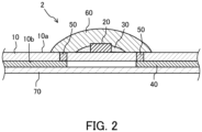
- Fig. 2 is a cross-sectional view for explaining a configuration of the RFID tag 2 according to a comparative example.
- the RFID tag 2 illustrated in Fig. 2 is different from the RFID tag 1 illustrated in Fig. 1 only in the positions of the through holes 50 (the positions of the two ends of the antenna pattern 40), the reference numerals of the respective parts are common to those of the RFID tag 1 illustrated in Fig. 1 .
- the through hole 50 of the RFID tag 2 does not penetrate the substrate 10 toward the conductive adhesive 30 around the substrate 10 but penetrates the substrate 10 toward the potting 60 around the conductive adhesive 30. Even in this case, as described above, the through hole 50 may be electrically connected to the bump of the IC chip 20 fixed by the conductive adhesive 30 via wiring (not illustrated) on the first face 10a of the substrate 10.
- the RFID tag 1 includes the sheet-like substrate 10, the IC chip 20 disposed on the first face 10a of the substrate 10, the conductive adhesive 30 that is positioned around the IC chip 20 along the first face 10a and fixes the IC chip 20 to the substrate 10, the antenna pattern 40 formed on the second face 10b, of the substrate 10, that is opposite to the first face 10a, and the through hole 50 that penetrates the substrate 10 toward the conductive adhesive 30 around the IC chip 20 and electrically connects the antenna pattern 40 with the IC chip 20.
- the antenna pattern 40 is formed on the second face 10b opposite to the first face 10a of the substrate 10 instead of on a face (first face 10a) same as a face on which the IC chip 20, the conductive adhesive 30, and the like are mounted, it is possible to suppress disconnection of the antenna pattern 40 due to stress concentrated on discontinuous points such as the periphery of the conductive adhesive 30 and the periphery of the potting 60.
- the protective layer 70 for protecting the antenna pattern 40 can also be provided on the second face 10b, it is possible to avoid stress concentration on an edge (end) of a hole when forming, for example, the circular hole in the protective layer 70 in order to avoid interference with the IC chip 20 and the conductive adhesive 30. As a result, it is also possible to avoid occurrence of disconnection in the antenna pattern 40 due to concentration of stress at the end of the protective layer 70.
- the antenna pattern 40 can be formed so as not to pass a position facing away from the IC chip 20. Therefore, it is also possible to avoid the stress concentrated on a position, of the second face 10b, facing away from the periphery of the IC chip 20 from affecting the antenna pattern 40.
- disconnection of the antenna pattern 40 can be suppressed. As a result, it is possible to suppress unresponsiveness or communication performance deterioration of the RFID tag 1.
- the antenna pattern 40 has two ends facing each other with a gap at a position of the second face 10b of the substrate 10, the position facing away from the IC chip 20, and the through hole 50 includes two through holes that electrically connect the two respective ends of the antenna pattern 40 and the IC chip 20.
- the antenna pattern 40 does not pass a position facing away from the IC chip 20, it is possible to avoid the stress concentrated on a position, of the second face 10b, facing away from the periphery of the IC chip 20 from affecting the antenna pattern 40 as described above.
- the present invention is not limited to the above-mentioned embodiment as it is, and can be embodied by modifying components thereof.
- various inventions can be formed by appropriately combining a plurality of components disclosed in the present embodiment.
- Various modifications of the invention and applications can be made without departing from the spirit of the invention.
Landscapes
- Engineering & Computer Science (AREA)
- Microelectronics & Electronic Packaging (AREA)
- Computer Hardware Design (AREA)
- Physics & Mathematics (AREA)
- General Physics & Mathematics (AREA)
- Theoretical Computer Science (AREA)
- Computer Networks & Wireless Communication (AREA)
- Credit Cards Or The Like (AREA)
- Details Of Aerials (AREA)
Abstract
Description
- The present invention relates to an RFID tag.
- In recent years, radio frequency identifier (RFID) tags have been attached to various objects, and the objects have been managed using information read from the RFID tags by a reader (see, for example,
Patent Literatures 1 and 2). For example, the RFID tag is used as an RFID label attached to an object and used. -
- Patent Literature 1:
JP 6485608 B - Patent Literature 2:
JP H7-146922 A -
Fig. 3 is a cross-sectional view for explaining a configuration of anRFID tag 101 according to the reference technique. -
Fig. 4 is a diagram illustrating a pattern example of anantenna pattern 140 in the reference technique. - The
RFID tag 101 illustrated inFig. 3 includes asubstrate 110, an integrated circuit (IC)chip 120, aconductive adhesive 130, theantenna pattern 140, apotting 160, and aprotective layer 170. - The
IC chip 120 is disposed on theantenna pattern 140 formed on thesubstrate 110, and is fixed by theconductive adhesive 130. - The
antenna pattern 140 is formed between thesubstrate 110 and theIC chip 120, and is formed in, for example, a loop shape as illustrated inFig. 4 . - The
potting 160 is disposed so as to cover theIC chip 120 and theconductive adhesive 130 in order to protect theIC chip 120. - The
protective layer 170 protects theantenna pattern 140. For example, theprotective layer 170 has a circular hole in order to avoid interference with theIC chip 120 and theconductive adhesive 130. Therefore, theprotective layer 170 is formed with a space between theIC chip 120 and theconductive adhesive 130. Part of theprotective layer 170 is covered with thepotting 160. - Physical stress is applied to such an
RFID tag 101, for example, when the RFID tag is attached to a linen product and washed together with the linen product. When this physical stress is applied to theRFID tag 101, stress is concentrated on a first stress concentration position P1 around thepotting 160, a second stress concentration position P2 at the end, of theprotective layer 170, adjacent to theIC chip 120, a third stress concentration position P3 around theconductive adhesive 130, and the like. This causes a problem that theantenna pattern 140 is disconnected, theRFID tag 101 is unresponsive or communication performance is deteriorated. - An object of the present invention is to provide an RFID tag capable of suppressing disconnection of an antenna pattern.
- An RFID tag of the disclosure includes a sheet-like substrate, an IC chip disposed on a first face of the substrate, a conductive adhesive that is positioned around the IC chip along the first face and fixes the IC chip to the substrate, an antenna pattern formed on a second face of the substrate, the second face being opposite to the first face, and at least one through hole that penetrates the substrate toward the conductive adhesive around the IC chip and electrically connects the antenna pattern with the IC chip.
- According to the RFID tag of the disclosure, disconnection of the antenna pattern can be suppressed.
-
-
Fig. 1 is a cross-sectional view for explaining a configuration of an RFID tag according to an embodiment; -
Fig. 2 is a cross-sectional view for explaining a configuration of an RFID tag according to a comparative example; -
Fig. 3 is a cross-sectional view for explaining a configuration of an RFID tag according to a reference technique; and -
Fig. 4 is a view illustrating a pattern example of an antenna pattern in the reference technique. - Hereinafter, an RFID tag according to an embodiment of the present invention will be described with reference to the drawings.
-
Fig. 1 is a cross-sectional view for explaining a configuration of anRFID tag 1 according to an embodiment. - The
RFID tag 1 illustrated inFig. 1 includes asubstrate 10, anIC chip 20, aconductive adhesive 30, anantenna pattern 40, two throughholes 50, apotting 60, and aprotective layer 70. - As an example, the
RFID tag 1 is used as part of an RFID label attached to an object. - The
substrate 10 is a sheet-like member, and is, for example, a film made of a synthetic resin material such as Polyethylene terephthalate (PET). Thesubstrate 10 preferably has flexibility from the viewpoint of durability. - The
IC chip 20 is disposed on afirst face 10a (upper face inFig. 1 ) of thesubstrate 10. TheIC chip 20 can be regarded as a large scale integration (LSI). - The
conductive adhesive 30 is an adhesive for fixing theIC chip 20 to thesubstrate 10, and has conductivity. Theconductive adhesive 30 is, for example, anisotropic conductive paste (ACP). For example, theconductive adhesive 30 is applied to thesubstrate 10 before theIC chip 20 is disposed on thesubstrate 10, and spreads from the bottom face of thesubstrate 10 along thefirst face 10a of thesubstrate 10 when theIC chip 20 is mounted. In this manner, theconductive adhesive 30 is positioned to spread around theIC chip 20 along thefirst face 10a of thesubstrate 10. - The
antenna pattern 40 is formed on asecond face 10b, of thesubstrate 10, that is opposite to thefirst face 10a. Theantenna pattern 40 is, for example, a dipole antenna, and has two ends facing each other with a gap at a position of thesecond face 10b of thesubstrate 10, the position facing away from theIC chip 20. That is, theantenna pattern 40 is not located at a position facing away from theIC chip 20 with thesubstrate 10 interposed between the position and the IC chip. Theantenna pattern 40 is made of, for example, silver paste. - The two through
holes 50 penetrate thesubstrate 10 toward theconductive adhesive 30 around theIC chip 20, and are provided to electrically connect theantenna pattern 40 with theIC chip 20. The throughhole 50 may be electrically connected to the bump of theIC chip 20 fixed by theconductive adhesive 30 via wiring (not illustrated) on thefirst face 10a of thesubstrate 10, for example. The throughhole 50 may be formed integrally with theantenna pattern 40. - The two through
holes 50 may penetrate thesubstrate 10 and communicate the above-described two ends of theantenna pattern 40 and theconductive adhesive 30. Depending on the shape of theantenna pattern 40, only one throughhole 50 may be provided, or three or more through holes may be provided. - The
potting 60 is provided on thefirst face 10a of thesubstrate 10 so as to cover theIC chip 20 and theconductive adhesive 30 in order to protect theIC chip 20. Thepotting 60 is made of, for example, a synthetic resin material. Note that thepotting 60 is an example of a reinforcing material that covers theIC chip 20 and theconductive adhesive 30. - The
protective layer 70 is a layer that protects theantenna pattern 40 formed on thesecond face 10b of thesubstrate 10, and is, for example, a resist layer. Theprotective layer 70 is made of, for example, a synthetic resin material. - In the
RFID tag 1 according to the present embodiment, as described above, theantenna pattern 40 is formed on thesecond face 10b opposite to thefirst face 10a, of thesubstrate 10, on which theconductive adhesive 30, thepotting 60, and the like are provided. - Therefore, even when the stress concentrates on the periphery of the potting 60 (the first stress concentration position P1 around the
potting 160 of the reference technique shown inFig. 3 ) or on the periphery of the conductive adhesive 30 (the stress concentration position P3 around the conductive adhesive 130), theantenna pattern 40 is not easily affected. In addition, since theprotective layer 70 together with theantenna pattern 40 is provided adjacent to thesecond face 10b, it is possible to cover theentire antenna pattern 40, and thus, unlike theprotective layer 170 of the reference technology illustrated inFig. 3 , it is possible to avoid stress concentration on the end (second stress concentration position P2) of theprotective layer 170. - Although the
antenna pattern 40 is formed on thesecond face 10b, the throughhole 50 penetrates thesubstrate 10 toward theconductive adhesive 30 instead of penetrating thesubstrate 10 toward theIC chip 20, so that theantenna pattern 40 can be formed so as not to pass a position facing away from theIC chip 20. Therefore, even when the stress concentrated around (peripheral edge) of theIC chip 20 affects thesecond face 10b on the back side via thesubstrate 10, theantenna pattern 40 is not affected by the stress. - Next, an
RFID tag 2 according to a comparative example will be described with reference toFig. 2 . -
Fig. 2 is a cross-sectional view for explaining a configuration of theRFID tag 2 according to a comparative example. - Since the
RFID tag 2 illustrated inFig. 2 is different from theRFID tag 1 illustrated inFig. 1 only in the positions of the through holes 50 (the positions of the two ends of the antenna pattern 40), the reference numerals of the respective parts are common to those of theRFID tag 1 illustrated inFig. 1 . - Unlike the through
hole 50 of theRFID tag 1, the throughhole 50 of theRFID tag 2 does not penetrate thesubstrate 10 toward theconductive adhesive 30 around thesubstrate 10 but penetrates thesubstrate 10 toward the potting 60 around theconductive adhesive 30. Even in this case, as described above, the throughhole 50 may be electrically connected to the bump of theIC chip 20 fixed by theconductive adhesive 30 via wiring (not illustrated) on thefirst face 10a of thesubstrate 10. - Even in such an
RFID tag 2, it can be said that even when the stress concentrates on the periphery of the potting 60 (the first stress concentration position P1 around the potting 160 of the reference technique shown inFig. 3 ) or on the periphery of the conductive adhesive 30 (the stress concentration position P3 around the conductive adhesive 130), theantenna pattern 40 is not easily affected. - However, since there is a gap between the through
hole 50, and theconductive adhesive 30 and theIC chip 20, stress tends to concentrate on wires on the periphery of theconductive adhesive 30 among wiring, (not illustrated) on thefirst face 10a of thesubstrate 10, disposed at this gap. - In the present embodiment described above, the
RFID tag 1 includes the sheet-like substrate 10, theIC chip 20 disposed on thefirst face 10a of thesubstrate 10, the conductive adhesive 30 that is positioned around theIC chip 20 along thefirst face 10a and fixes theIC chip 20 to thesubstrate 10, theantenna pattern 40 formed on thesecond face 10b, of thesubstrate 10, that is opposite to thefirst face 10a, and the throughhole 50 that penetrates thesubstrate 10 toward theconductive adhesive 30 around theIC chip 20 and electrically connects theantenna pattern 40 with theIC chip 20. - As described above, by forming the
antenna pattern 40 on thesecond face 10b opposite to thefirst face 10a of thesubstrate 10 instead of on a face (first face 10a) same as a face on which theIC chip 20, theconductive adhesive 30, and the like are mounted, it is possible to suppress disconnection of theantenna pattern 40 due to stress concentrated on discontinuous points such as the periphery of theconductive adhesive 30 and the periphery of thepotting 60. - In addition, since the
protective layer 70 for protecting theantenna pattern 40 can also be provided on thesecond face 10b, it is possible to avoid stress concentration on an edge (end) of a hole when forming, for example, the circular hole in theprotective layer 70 in order to avoid interference with theIC chip 20 and theconductive adhesive 30. As a result, it is also possible to avoid occurrence of disconnection in theantenna pattern 40 due to concentration of stress at the end of theprotective layer 70. - Furthermore, since the through
hole 50 does not penetrate thesubstrate 10 toward theIC chip 20 but penetrates thesubstrate 10 toward theconductive adhesive 30, theantenna pattern 40 can be formed so as not to pass a position facing away from theIC chip 20. Therefore, it is also possible to avoid the stress concentrated on a position, of thesecond face 10b, facing away from the periphery of theIC chip 20 from affecting theantenna pattern 40. - Therefore, according to the present embodiment, disconnection of the
antenna pattern 40 can be suppressed. As a result, it is possible to suppress unresponsiveness or communication performance deterioration of theRFID tag 1. - In addition, in the present embodiment, the
antenna pattern 40 has two ends facing each other with a gap at a position of thesecond face 10b of thesubstrate 10, the position facing away from theIC chip 20, and the throughhole 50 includes two through holes that electrically connect the two respective ends of theantenna pattern 40 and theIC chip 20. - In this way, since the
antenna pattern 40 does not pass a position facing away from theIC chip 20, it is possible to avoid the stress concentrated on a position, of thesecond face 10b, facing away from the periphery of theIC chip 20 from affecting theantenna pattern 40 as described above. - Note that the present invention is not limited to the above-mentioned embodiment as it is, and can be embodied by modifying components thereof. For example, various inventions can be formed by appropriately combining a plurality of components disclosed in the present embodiment. Various modifications of the invention and applications can be made without departing from the spirit of the invention.
-
- 1
- RFID tag
- 10
- substrate
- 10a
- first face
- 10b
- second face
- 20
- IC chip
- 30
- conductive adhesive
- 40
- antenna pattern
- 50
- through hole
- 60
- potting
- 70
- protective layer
Claims (2)
- An RFID tag comprising:a sheet-like substrate;an IC chip disposed on a first face of the substrate;a conductive adhesive that is positioned around the IC chip along the first face and fixes the IC chip to the substrate;an antenna pattern formed on a second face of the substrate, the second face being opposite to the first face; andat least one through hole that penetrates the substrate toward the conductive adhesive around the IC chip and electrically connects the antenna pattern with the IC chip.
- The RFID tag according to claim 1, whereinthe antenna pattern has two ends facing each other with a gap at a position of the second face of the substrate, the position facing away from the IC chip, andthe at least one through hole comprises two through holes that electrically connect the two respective ends of the antenna pattern with the IC chip.
Applications Claiming Priority (1)
| Application Number | Priority Date | Filing Date | Title |
|---|---|---|---|
| PCT/JP2021/006003 WO2022176080A1 (en) | 2021-02-17 | 2021-02-17 | Rfid tag |
Publications (2)
| Publication Number | Publication Date |
|---|---|
| EP4296894A1 true EP4296894A1 (en) | 2023-12-27 |
| EP4296894A4 EP4296894A4 (en) | 2024-04-03 |
Family
ID=82930364
Family Applications (1)
| Application Number | Title | Priority Date | Filing Date |
|---|---|---|---|
| EP21926518.8A Pending EP4296894A4 (en) | 2021-02-17 | 2021-02-17 | Rfid tag |
Country Status (5)
| Country | Link |
|---|---|
| US (1) | US12462139B2 (en) |
| EP (1) | EP4296894A4 (en) |
| JP (1) | JP7487401B2 (en) |
| CN (1) | CN116745775A (en) |
| WO (1) | WO2022176080A1 (en) |
Families Citing this family (2)
| Publication number | Priority date | Publication date | Assignee | Title |
|---|---|---|---|---|
| JP7487401B2 (en) * | 2021-02-17 | 2024-05-20 | 富士通フロンテック株式会社 | RFID tags |
| CN119761401A (en) * | 2024-04-03 | 2025-04-04 | 上海数佑信息科技有限公司 | RFID tag component and tool having RFID tag component |
Family Cites Families (37)
| Publication number | Priority date | Publication date | Assignee | Title |
|---|---|---|---|---|
| JPH07146922A (en) | 1993-09-28 | 1995-06-06 | Dainippon Printing Co Ltd | Non-contact type IC module, non-contact type IC card and manufacturing method thereof |
| JPH1032304A (en) * | 1996-07-16 | 1998-02-03 | Oki Electric Ind Co Ltd | Bus wiring structure in mounting semiconductor integrated circuit devices |
| JP3936840B2 (en) * | 1997-12-22 | 2007-06-27 | 株式会社日立製作所 | Semiconductor device and manufacturing method thereof |
| US6100804A (en) * | 1998-10-29 | 2000-08-08 | Intecmec Ip Corp. | Radio frequency identification system |
| JP2001043336A (en) * | 1999-07-29 | 2001-02-16 | Sony Chem Corp | Ic card |
| US6421013B1 (en) * | 1999-10-04 | 2002-07-16 | Amerasia International Technology, Inc. | Tamper-resistant wireless article including an antenna |
| US7049962B2 (en) * | 2000-07-28 | 2006-05-23 | Micoh Corporation | Materials and construction for a tamper indicating radio frequency identification label |
| JP2002074304A (en) * | 2000-09-05 | 2002-03-15 | Dainippon Printing Co Ltd | Non-contact IC card and method of manufacturing the same |
| US6774470B2 (en) * | 2001-12-28 | 2004-08-10 | Dai Nippon Printing Co., Ltd. | Non-contact data carrier and method of fabricating the same |
| JP3979873B2 (en) * | 2001-12-28 | 2007-09-19 | 大日本印刷株式会社 | Non-contact data carrier manufacturing method |
| JP2004133762A (en) * | 2002-10-11 | 2004-04-30 | Yoshikawa Rf System Kk | Data carrier and its manufacturing method |
| JP2004165531A (en) * | 2002-11-15 | 2004-06-10 | Dainippon Printing Co Ltd | Double-sided wiring antenna circuit member for non-contact data carrier |
| JP4768379B2 (en) * | 2005-09-28 | 2011-09-07 | 富士通株式会社 | RFID tag |
| US7808384B2 (en) * | 2006-07-14 | 2010-10-05 | Eyes Open Corporation | Information carrier arrangement, washable textile goods and electronic ear tag for living beings |
| JP5470680B2 (en) * | 2007-02-06 | 2014-04-16 | 日亜化学工業株式会社 | LIGHT EMITTING DEVICE, MANUFACTURING METHOD THEREOF, AND MOLDED BODY |
| JP5145881B2 (en) * | 2007-11-07 | 2013-02-20 | 富士通株式会社 | RFID tag |
| DE102008024823A1 (en) * | 2008-05-23 | 2009-12-10 | Smartrac Ip B.V. | Chip card with a plurality of components |
| JP5182512B2 (en) * | 2008-12-15 | 2013-04-17 | 日亜化学工業株式会社 | Thermosetting epoxy resin composition and semiconductor device |
| DE102010024523B4 (en) * | 2010-06-21 | 2017-03-23 | Leonhard Kurz Stiftung & Co. Kg | Multilayer film element |
| JP2012032931A (en) * | 2010-07-29 | 2012-02-16 | Hitachi Ltd | Rfid tag and method for manufacturing rfid tag |
| US11928537B2 (en) * | 2013-01-18 | 2024-03-12 | Amatech Group Limited | Manufacturing metal inlays for dual interface metal cards |
| US9275322B2 (en) * | 2013-11-25 | 2016-03-01 | VivaLnk Limited (Cayman Islands) | Stretchable multi-layer wearable tag capable of wireless communications |
| DE102014107299B4 (en) * | 2014-05-23 | 2019-03-28 | Infineon Technologies Ag | Smart card module, smart card, and method of manufacturing a smart card module |
| CN106471524B (en) * | 2015-06-18 | 2019-07-30 | 株式会社村田制作所 | Carrier tape, method for manufacturing the same, and method for manufacturing RFID tag |
| JP6679244B2 (en) * | 2015-08-27 | 2020-04-15 | 富士通株式会社 | RFID tag |
| US10320054B2 (en) * | 2016-10-28 | 2019-06-11 | Avery Dennison Retail Information Services, Llc | RFID tags designed to work on difficult substrates |
| JP6197133B1 (en) * | 2017-02-03 | 2017-09-13 | 日本パッケージ・システム株式会社 | Method for manufacturing antenna sheet and method for manufacturing non-contact IC tag |
| CN212676453U (en) * | 2017-04-18 | 2021-03-09 | 株式会社村田制作所 | RFID tag |
| WO2018199007A1 (en) * | 2017-04-28 | 2018-11-01 | 株式会社村田製作所 | Rfid tag |
| WO2019012767A1 (en) * | 2017-07-14 | 2019-01-17 | 株式会社村田製作所 | Rfid tag and rfid tag management method |
| JP6610849B1 (en) * | 2018-09-05 | 2019-11-27 | 株式会社村田製作所 | RFIC module, RFID tag and article |
| FR3088515B1 (en) * | 2018-11-08 | 2022-01-28 | Smart Packaging Solutions | ELECTRONIC MODULE FOR CHIP CARD |
| US20200202192A1 (en) * | 2018-12-20 | 2020-06-25 | Shenzhen Leadercolor Smart Card Co., Ltd | Attached-type smart label |
| CN114424679A (en) * | 2019-09-24 | 2022-04-29 | 3M创新有限公司 | Method and apparatus for interconnection using microchannels |
| SE543748C2 (en) * | 2019-11-08 | 2021-07-13 | Stora Enso Oyj | Rfid label |
| DE212020000366U1 (en) * | 2019-11-25 | 2021-02-23 | Murata Manufacturing Co., Ltd. | RFIC module and RFID transponder |
| JP7487401B2 (en) * | 2021-02-17 | 2024-05-20 | 富士通フロンテック株式会社 | RFID tags |
-
2021
- 2021-02-17 JP JP2023500198A patent/JP7487401B2/en active Active
- 2021-02-17 EP EP21926518.8A patent/EP4296894A4/en active Pending
- 2021-02-17 CN CN202180091838.4A patent/CN116745775A/en active Pending
- 2021-02-17 WO PCT/JP2021/006003 patent/WO2022176080A1/en not_active Ceased
-
2023
- 2023-07-25 US US18/358,412 patent/US12462139B2/en active Active
Also Published As
| Publication number | Publication date |
|---|---|
| JP7487401B2 (en) | 2024-05-20 |
| CN116745775A (en) | 2023-09-12 |
| JPWO2022176080A1 (en) | 2022-08-25 |
| US20240046061A1 (en) | 2024-02-08 |
| US12462139B2 (en) | 2025-11-04 |
| WO2022176080A1 (en) | 2022-08-25 |
| EP4296894A4 (en) | 2024-04-03 |
Similar Documents
| Publication | Publication Date | Title |
|---|---|---|
| US12462139B2 (en) | RFID tag | |
| EP4022511B1 (en) | Rotation-insensitive rfid devices and methods of forming the same | |
| CN101636837B (en) | Electronic device, electronic apparatus mounting electronic device, article mounting electronic device, and method for manufacturing electronic device | |
| CA2621574C (en) | Rfid transponder | |
| US8068031B2 (en) | RFID devices and methods for overlapped objects | |
| KR20040098665A (en) | Integrated circuit with enhanced coupling | |
| US7982295B2 (en) | Electronic device, electronic apparatus mounted with electronic device, article equipped with electronic device and method of producing electronic device | |
| US7789316B2 (en) | Electronic device, electronic apparatus mounted with electronic device, article equipped with electronic device and method of producing electronic device | |
| US20090115577A1 (en) | Rfid tag | |
| KR20010101143A (en) | Non-contact data carrier and ic chip | |
| US9972884B2 (en) | RFID tag | |
| KR20050094082A (en) | Eyelet for a radio frequency identification | |
| US7364088B2 (en) | Radio frequency identification tag | |
| EP2278533B1 (en) | RFID tag | |
| US20100038765A1 (en) | Semiconductor package and method for manufacturing the same | |
| US20080204250A1 (en) | RFID tag | |
| KR101025771B1 (en) | RFID tag and manufacturing method thereof | |
| US20210175142A1 (en) | Integrated circuit (ic) tag | |
| EP3561731A1 (en) | Rfid tag | |
| CN105989396A (en) | Electronic tag | |
| US12468916B2 (en) | RFID (radio frequency identification) tag, in particular for washable items | |
| KR102508828B1 (en) | Cof package | |
| US8867223B2 (en) | System and method for a high retention module interface | |
| KR20150030438A (en) | Rfid assembly | |
| KR20050081538A (en) | Rf-tbga(radio frequency-taped ball grid array) module |
Legal Events
| Date | Code | Title | Description |
|---|---|---|---|
| STAA | Information on the status of an ep patent application or granted ep patent |
Free format text: STATUS: THE INTERNATIONAL PUBLICATION HAS BEEN MADE |
|
| PUAI | Public reference made under article 153(3) epc to a published international application that has entered the european phase |
Free format text: ORIGINAL CODE: 0009012 |
|
| STAA | Information on the status of an ep patent application or granted ep patent |
Free format text: STATUS: REQUEST FOR EXAMINATION WAS MADE |
|
| 17P | Request for examination filed |
Effective date: 20230726 |
|
| AK | Designated contracting states |
Kind code of ref document: A1 Designated state(s): AL AT BE BG CH CY CZ DE DK EE ES FI FR GB GR HR HU IE IS IT LI LT LU LV MC MK MT NL NO PL PT RO RS SE SI SK SM TR |
|
| A4 | Supplementary search report drawn up and despatched |
Effective date: 20240304 |
|
| RIC1 | Information provided on ipc code assigned before grant |
Ipc: G06K 19/077 20060101AFI20240227BHEP |
|
| DAV | Request for validation of the european patent (deleted) | ||
| DAX | Request for extension of the european patent (deleted) | ||
| STAA | Information on the status of an ep patent application or granted ep patent |
Free format text: STATUS: EXAMINATION IS IN PROGRESS |
|
| 17Q | First examination report despatched |
Effective date: 20250704 |