EP4296747A2 - Anzeigevorrichtung und verfahren zur steuerung davon - Google Patents
Anzeigevorrichtung und verfahren zur steuerung davon Download PDFInfo
- Publication number
- EP4296747A2 EP4296747A2 EP23180167.1A EP23180167A EP4296747A2 EP 4296747 A2 EP4296747 A2 EP 4296747A2 EP 23180167 A EP23180167 A EP 23180167A EP 4296747 A2 EP4296747 A2 EP 4296747A2
- Authority
- EP
- European Patent Office
- Prior art keywords
- display panel
- display
- image
- sub
- light
- Prior art date
- Legal status (The legal status is an assumption and is not a legal conclusion. Google has not performed a legal analysis and makes no representation as to the accuracy of the status listed.)
- Pending
Links
Images











Classifications
-
- H—ELECTRICITY
- H10—SEMICONDUCTOR DEVICES; ELECTRIC SOLID-STATE DEVICES NOT OTHERWISE PROVIDED FOR
- H10K—ORGANIC ELECTRIC SOLID-STATE DEVICES
- H10K59/00—Integrated devices, or assemblies of multiple devices, comprising at least one organic light-emitting element covered by group H10K50/00
- H10K59/50—OLEDs integrated with light modulating elements, e.g. with electrochromic elements, photochromic elements or liquid crystal elements
-
- H—ELECTRICITY
- H10—SEMICONDUCTOR DEVICES; ELECTRIC SOLID-STATE DEVICES NOT OTHERWISE PROVIDED FOR
- H10K—ORGANIC ELECTRIC SOLID-STATE DEVICES
- H10K59/00—Integrated devices, or assemblies of multiple devices, comprising at least one organic light-emitting element covered by group H10K50/00
- H10K59/80—Constructional details
- H10K59/875—Arrangements for extracting light from the devices
- H10K59/879—Arrangements for extracting light from the devices comprising refractive means, e.g. lenses
-
- G—PHYSICS
- G02—OPTICS
- G02B—OPTICAL ELEMENTS, SYSTEMS OR APPARATUS
- G02B27/00—Optical systems or apparatus not provided for by any of the groups G02B1/00 - G02B26/00, G02B30/00
- G02B27/01—Head-up displays
- G02B27/017—Head mounted
- G02B27/0172—Head mounted characterised by optical features
-
- G—PHYSICS
- G02—OPTICS
- G02B—OPTICAL ELEMENTS, SYSTEMS OR APPARATUS
- G02B17/00—Systems with reflecting surfaces, with or without refracting elements
- G02B17/08—Catadioptric systems
- G02B17/0804—Catadioptric systems using two curved mirrors
- G02B17/0816—Catadioptric systems using two curved mirrors off-axis or unobscured systems in which not all of the mirrors share a common axis of rotational symmetry, e.g. at least one of the mirrors is warped, tilted or decentered with respect to the other elements
-
- G—PHYSICS
- G02—OPTICS
- G02B—OPTICAL ELEMENTS, SYSTEMS OR APPARATUS
- G02B17/00—Systems with reflecting surfaces, with or without refracting elements
- G02B17/08—Catadioptric systems
- G02B17/0856—Catadioptric systems comprising a refractive element with a reflective surface, the reflection taking place inside the element, e.g. Mangin mirrors
- G02B17/086—Catadioptric systems comprising a refractive element with a reflective surface, the reflection taking place inside the element, e.g. Mangin mirrors wherein the system is made of a single block of optical material, e.g. solid catadioptric systems
-
- G—PHYSICS
- G02—OPTICS
- G02B—OPTICAL ELEMENTS, SYSTEMS OR APPARATUS
- G02B25/00—Eyepieces; Magnifying glasses
- G02B25/001—Eyepieces
-
- G—PHYSICS
- G02—OPTICS
- G02B—OPTICAL ELEMENTS, SYSTEMS OR APPARATUS
- G02B25/00—Eyepieces; Magnifying glasses
- G02B25/002—Magnifying glasses
-
- G—PHYSICS
- G02—OPTICS
- G02B—OPTICAL ELEMENTS, SYSTEMS OR APPARATUS
- G02B26/00—Optical devices or arrangements for the control of light using movable or deformable optical elements
- G02B26/08—Optical devices or arrangements for the control of light using movable or deformable optical elements for controlling the direction of light
-
- G—PHYSICS
- G02—OPTICS
- G02B—OPTICAL ELEMENTS, SYSTEMS OR APPARATUS
- G02B27/00—Optical systems or apparatus not provided for by any of the groups G02B1/00 - G02B26/00, G02B30/00
- G02B27/0018—Optical systems or apparatus not provided for by any of the groups G02B1/00 - G02B26/00, G02B30/00 with means for preventing ghost images
-
- G—PHYSICS
- G02—OPTICS
- G02B—OPTICAL ELEMENTS, SYSTEMS OR APPARATUS
- G02B27/00—Optical systems or apparatus not provided for by any of the groups G02B1/00 - G02B26/00, G02B30/00
- G02B27/0093—Optical systems or apparatus not provided for by any of the groups G02B1/00 - G02B26/00, G02B30/00 with means for monitoring data relating to the user, e.g. head-tracking, eye-tracking
-
- G—PHYSICS
- G06—COMPUTING OR CALCULATING; COUNTING
- G06F—ELECTRIC DIGITAL DATA PROCESSING
- G06F1/00—Details not covered by groups G06F3/00 - G06F13/00 and G06F21/00
- G06F1/16—Constructional details or arrangements
- G06F1/1613—Constructional details or arrangements for portable computers
- G06F1/163—Wearable computers, e.g. on a belt
-
- G—PHYSICS
- G06—COMPUTING OR CALCULATING; COUNTING
- G06F—ELECTRIC DIGITAL DATA PROCESSING
- G06F1/00—Details not covered by groups G06F3/00 - G06F13/00 and G06F21/00
- G06F1/16—Constructional details or arrangements
- G06F1/1613—Constructional details or arrangements for portable computers
- G06F1/1633—Constructional details or arrangements of portable computers not specific to the type of enclosures covered by groups G06F1/1615 - G06F1/1626
- G06F1/1637—Details related to the display arrangement, including those related to the mounting of the display in the housing
-
- G—PHYSICS
- G06—COMPUTING OR CALCULATING; COUNTING
- G06F—ELECTRIC DIGITAL DATA PROCESSING
- G06F3/00—Input arrangements for transferring data to be processed into a form capable of being handled by the computer; Output arrangements for transferring data from processing unit to output unit, e.g. interface arrangements
- G06F3/01—Input arrangements or combined input and output arrangements for interaction between user and computer
- G06F3/011—Arrangements for interaction with the human body, e.g. for user immersion in virtual reality
- G06F3/013—Eye tracking input arrangements
-
- G—PHYSICS
- G09—EDUCATION; CRYPTOGRAPHY; DISPLAY; ADVERTISING; SEALS
- G09G—ARRANGEMENTS OR CIRCUITS FOR CONTROL OF INDICATING DEVICES USING STATIC MEANS TO PRESENT VARIABLE INFORMATION
- G09G3/00—Control arrangements or circuits, of interest only in connection with visual indicators other than cathode-ray tubes
- G09G3/001—Control arrangements or circuits, of interest only in connection with visual indicators other than cathode-ray tubes using specific devices not provided for in groups G09G3/02 - G09G3/36, e.g. using an intermediate record carrier such as a film slide; Projection systems; Display of non-alphanumerical information, solely or in combination with alphanumerical information, e.g. digital display on projected diapositive as background
-
- G—PHYSICS
- G09—EDUCATION; CRYPTOGRAPHY; DISPLAY; ADVERTISING; SEALS
- G09G—ARRANGEMENTS OR CIRCUITS FOR CONTROL OF INDICATING DEVICES USING STATIC MEANS TO PRESENT VARIABLE INFORMATION
- G09G3/00—Control arrangements or circuits, of interest only in connection with visual indicators other than cathode-ray tubes
- G09G3/20—Control arrangements or circuits, of interest only in connection with visual indicators other than cathode-ray tubes for presentation of an assembly of a number of characters, e.g. a page, by composing the assembly by combination of individual elements arranged in a matrix no fixed position being assigned to or needed to be assigned to the individual characters or partial characters
- G09G3/22—Control arrangements or circuits, of interest only in connection with visual indicators other than cathode-ray tubes for presentation of an assembly of a number of characters, e.g. a page, by composing the assembly by combination of individual elements arranged in a matrix no fixed position being assigned to or needed to be assigned to the individual characters or partial characters using controlled light sources
- G09G3/30—Control arrangements or circuits, of interest only in connection with visual indicators other than cathode-ray tubes for presentation of an assembly of a number of characters, e.g. a page, by composing the assembly by combination of individual elements arranged in a matrix no fixed position being assigned to or needed to be assigned to the individual characters or partial characters using controlled light sources using electroluminescent panels
- G09G3/32—Control arrangements or circuits, of interest only in connection with visual indicators other than cathode-ray tubes for presentation of an assembly of a number of characters, e.g. a page, by composing the assembly by combination of individual elements arranged in a matrix no fixed position being assigned to or needed to be assigned to the individual characters or partial characters using controlled light sources using electroluminescent panels semiconductive, e.g. using light-emitting diodes [LED]
- G09G3/3208—Control arrangements or circuits, of interest only in connection with visual indicators other than cathode-ray tubes for presentation of an assembly of a number of characters, e.g. a page, by composing the assembly by combination of individual elements arranged in a matrix no fixed position being assigned to or needed to be assigned to the individual characters or partial characters using controlled light sources using electroluminescent panels semiconductive, e.g. using light-emitting diodes [LED] organic, e.g. using organic light-emitting diodes [OLED]
- G09G3/3225—Control arrangements or circuits, of interest only in connection with visual indicators other than cathode-ray tubes for presentation of an assembly of a number of characters, e.g. a page, by composing the assembly by combination of individual elements arranged in a matrix no fixed position being assigned to or needed to be assigned to the individual characters or partial characters using controlled light sources using electroluminescent panels semiconductive, e.g. using light-emitting diodes [LED] organic, e.g. using organic light-emitting diodes [OLED] using an active matrix
- G09G3/3233—Control arrangements or circuits, of interest only in connection with visual indicators other than cathode-ray tubes for presentation of an assembly of a number of characters, e.g. a page, by composing the assembly by combination of individual elements arranged in a matrix no fixed position being assigned to or needed to be assigned to the individual characters or partial characters using controlled light sources using electroluminescent panels semiconductive, e.g. using light-emitting diodes [LED] organic, e.g. using organic light-emitting diodes [OLED] using an active matrix with pixel circuitry controlling the current through the light-emitting element
-
- H—ELECTRICITY
- H04—ELECTRIC COMMUNICATION TECHNIQUE
- H04N—PICTORIAL COMMUNICATION, e.g. TELEVISION
- H04N13/00—Stereoscopic video systems; Multi-view video systems; Details thereof
- H04N13/30—Image reproducers
- H04N13/332—Displays for viewing with the aid of special glasses or head-mounted displays [HMD]
-
- H—ELECTRICITY
- H10—SEMICONDUCTOR DEVICES; ELECTRIC SOLID-STATE DEVICES NOT OTHERWISE PROVIDED FOR
- H10K—ORGANIC ELECTRIC SOLID-STATE DEVICES
- H10K50/00—Organic light-emitting devices
- H10K50/80—Constructional details
- H10K50/85—Arrangements for extracting light from the devices
- H10K50/858—Arrangements for extracting light from the devices comprising refractive means, e.g. lenses
-
- H—ELECTRICITY
- H10—SEMICONDUCTOR DEVICES; ELECTRIC SOLID-STATE DEVICES NOT OTHERWISE PROVIDED FOR
- H10K—ORGANIC ELECTRIC SOLID-STATE DEVICES
- H10K59/00—Integrated devices, or assemblies of multiple devices, comprising at least one organic light-emitting element covered by group H10K50/00
- H10K59/90—Assemblies of multiple devices comprising at least one organic light-emitting element
-
- G—PHYSICS
- G02—OPTICS
- G02B—OPTICAL ELEMENTS, SYSTEMS OR APPARATUS
- G02B27/00—Optical systems or apparatus not provided for by any of the groups G02B1/00 - G02B26/00, G02B30/00
- G02B27/01—Head-up displays
- G02B27/0101—Head-up displays characterised by optical features
- G02B2027/0132—Head-up displays characterised by optical features comprising binocular systems
- G02B2027/0134—Head-up displays characterised by optical features comprising binocular systems of stereoscopic type
-
- G—PHYSICS
- G02—OPTICS
- G02B—OPTICAL ELEMENTS, SYSTEMS OR APPARATUS
- G02B27/00—Optical systems or apparatus not provided for by any of the groups G02B1/00 - G02B26/00, G02B30/00
- G02B27/01—Head-up displays
- G02B27/0101—Head-up displays characterised by optical features
- G02B2027/0138—Head-up displays characterised by optical features comprising image capture systems, e.g. camera
-
- G—PHYSICS
- G02—OPTICS
- G02B—OPTICAL ELEMENTS, SYSTEMS OR APPARATUS
- G02B27/00—Optical systems or apparatus not provided for by any of the groups G02B1/00 - G02B26/00, G02B30/00
- G02B27/01—Head-up displays
- G02B27/0101—Head-up displays characterised by optical features
- G02B2027/014—Head-up displays characterised by optical features comprising information/image processing systems
-
- G—PHYSICS
- G02—OPTICS
- G02B—OPTICAL ELEMENTS, SYSTEMS OR APPARATUS
- G02B27/00—Optical systems or apparatus not provided for by any of the groups G02B1/00 - G02B26/00, G02B30/00
- G02B27/01—Head-up displays
- G02B27/0101—Head-up displays characterised by optical features
- G02B2027/0147—Head-up displays characterised by optical features comprising a device modifying the resolution of the displayed image
-
- G—PHYSICS
- G02—OPTICS
- G02B—OPTICAL ELEMENTS, SYSTEMS OR APPARATUS
- G02B27/00—Optical systems or apparatus not provided for by any of the groups G02B1/00 - G02B26/00, G02B30/00
- G02B27/01—Head-up displays
- G02B27/0179—Display position adjusting means not related to the information to be displayed
- G02B2027/0187—Display position adjusting means not related to the information to be displayed slaved to motion of at least a part of the body of the user, e.g. head, eye
-
- G—PHYSICS
- G02—OPTICS
- G02B—OPTICAL ELEMENTS, SYSTEMS OR APPARATUS
- G02B27/00—Optical systems or apparatus not provided for by any of the groups G02B1/00 - G02B26/00, G02B30/00
- G02B27/28—Optical systems or apparatus not provided for by any of the groups G02B1/00 - G02B26/00, G02B30/00 for polarising
- G02B27/283—Optical systems or apparatus not provided for by any of the groups G02B1/00 - G02B26/00, G02B30/00 for polarising used for beam splitting or combining
-
- G—PHYSICS
- G06—COMPUTING OR CALCULATING; COUNTING
- G06F—ELECTRIC DIGITAL DATA PROCESSING
- G06F3/00—Input arrangements for transferring data to be processed into a form capable of being handled by the computer; Output arrangements for transferring data from processing unit to output unit, e.g. interface arrangements
- G06F3/14—Digital output to display device ; Cooperation and interconnection of the display device with other functional units
- G06F3/147—Digital output to display device ; Cooperation and interconnection of the display device with other functional units using display panels
-
- G—PHYSICS
- G09—EDUCATION; CRYPTOGRAPHY; DISPLAY; ADVERTISING; SEALS
- G09G—ARRANGEMENTS OR CIRCUITS FOR CONTROL OF INDICATING DEVICES USING STATIC MEANS TO PRESENT VARIABLE INFORMATION
- G09G2300/00—Aspects of the constitution of display devices
- G09G2300/02—Composition of display devices
- G09G2300/023—Display panel composed of stacked panels
-
- G—PHYSICS
- G09—EDUCATION; CRYPTOGRAPHY; DISPLAY; ADVERTISING; SEALS
- G09G—ARRANGEMENTS OR CIRCUITS FOR CONTROL OF INDICATING DEVICES USING STATIC MEANS TO PRESENT VARIABLE INFORMATION
- G09G2300/00—Aspects of the constitution of display devices
- G09G2300/04—Structural and physical details of display devices
- G09G2300/0439—Pixel structures
- G09G2300/0465—Improved aperture ratio, e.g. by size reduction of the pixel circuit, e.g. for improving the pixel density or the maximum displayable luminance or brightness
-
- G—PHYSICS
- G09—EDUCATION; CRYPTOGRAPHY; DISPLAY; ADVERTISING; SEALS
- G09G—ARRANGEMENTS OR CIRCUITS FOR CONTROL OF INDICATING DEVICES USING STATIC MEANS TO PRESENT VARIABLE INFORMATION
- G09G2340/00—Aspects of display data processing
- G09G2340/04—Changes in size, position or resolution of an image
- G09G2340/0407—Resolution change, inclusive of the use of different resolutions for different screen areas
-
- G—PHYSICS
- G09—EDUCATION; CRYPTOGRAPHY; DISPLAY; ADVERTISING; SEALS
- G09G—ARRANGEMENTS OR CIRCUITS FOR CONTROL OF INDICATING DEVICES USING STATIC MEANS TO PRESENT VARIABLE INFORMATION
- G09G2340/00—Aspects of display data processing
- G09G2340/12—Overlay of images, i.e. displayed pixel being the result of switching between the corresponding input pixels
-
- G—PHYSICS
- G09—EDUCATION; CRYPTOGRAPHY; DISPLAY; ADVERTISING; SEALS
- G09G—ARRANGEMENTS OR CIRCUITS FOR CONTROL OF INDICATING DEVICES USING STATIC MEANS TO PRESENT VARIABLE INFORMATION
- G09G2354/00—Aspects of interface with display user
-
- H—ELECTRICITY
- H10—SEMICONDUCTOR DEVICES; ELECTRIC SOLID-STATE DEVICES NOT OTHERWISE PROVIDED FOR
- H10K—ORGANIC ELECTRIC SOLID-STATE DEVICES
- H10K59/00—Integrated devices, or assemblies of multiple devices, comprising at least one organic light-emitting element covered by group H10K50/00
- H10K59/10—OLED displays
- H10K59/12—Active-matrix OLED [AMOLED] displays
-
- H—ELECTRICITY
- H10—SEMICONDUCTOR DEVICES; ELECTRIC SOLID-STATE DEVICES NOT OTHERWISE PROVIDED FOR
- H10W—GENERIC PACKAGES, INTERCONNECTIONS, CONNECTORS OR OTHER CONSTRUCTIONAL DETAILS OF DEVICES COVERED BY CLASS H10
- H10W90/00—Package configurations
Definitions
- the display devices there are electronic devices provided in a form that can be worn on the body. Such electronic devices are typically referred to as wearable devices.
- the wearable electronic device is directly worn on the body, thus improving portability and user accessibility.
- Each of the first sub-display panel and the second sub-display panel may have a viewing angle of about 20° to about 80°, and each of the third sub-display panel and the fourth sub-display panel has a viewing angle of about 1° to about 20°.
- a display device includes: a first display panel having a first resolution; a second display panel having a second resolution; a first multi-channel lens and a second multi-channel lens disposed on one surface of the first display panel and comprising a plurality of channels through which light emitted from the one surface of the first display panel passes; an eye tracking unit configured to detect a user's gaze direction; and a light steerer configured to control a direction of light emitted from the second display panel based on the gaze direction, where the second resolution is higher than the first resolution and the second display panel overlaps the first display panel in a plan view.
- the first display panel may be a transparent display panel
- the second display panel may be disposed on the other surface of the first display panel opposite to the one surface, and the light emitted from the second display panel may be transmitted through the first display panel.
- the first display panel may display a first display image
- the second display panel may display a second display image
- the first display image may be an image in which an area overlapping the second display image in the plan view is cut out.
- the light steerer may be disposed between the first display panel and the second display panel.
- the light steerer may be a deflector.
- the eye tracking unit may include: a plurality of infrared light sources disposed on the one surface of the first display panel and for emitting infrared rays; and a plurality of infrared cameras configured to sense infrared rays reflected from the user's pupil after being emitted from the infrared light sources.
- the first display panel may include a transmission region configured to transmit infrared rays incident on the one surface, and the plurality of infrared cameras may be disposed on the other surface of the first display panel to overlap the transmission region in the plan view.
- a display device includes: a first display panel having a first resolution; a second display panel having a second resolution and not overlapping the first display panel in a thickness direction of the first display panel; a first multi-channel lens and a second multi-channel lens disposed on one surface of the first display panel and comprising a plurality of channels through which light emitted from the one surface of the first display panel passes; an eye tracking unit configured to detect a user's gaze direction; and an optical path changing member disposed on an optical path of light emitted from the second display panel to control a direction of the light emitted from the second display panel based on the gaze direction, where the second resolution is higher than the first resolution.
- the second display panel may have about twice as many pixels per inch (PPI) as the first display panel.
- PPI pixels per inch
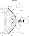
- the optical path changing member may include a half mirror (ML) and a concave mirror (CCL).
- ML half mirror
- CCL concave mirror
- the half mirror (ML) may be disposed between the second display panel and the concave mirror (CCL), transmit light incident from the second display panel, and reflect incident light reflected from the concave mirror (CCL).
- the display device may further include at least one light magnification member between the second display panel and the half mirror (ML).
- the light magnification member may be any one of a convex lens and a concave lens.
- the display device may further include: a reflective polarization film disposed on a surface of the half mirror on which the light reflected from the concave mirror is incident; and a phase delay element disposed in parallel with the half mirror.
- the first display panel may display a first display image
- the second display panel displays a second display image
- the first display image is an image in which an area overlapping the second display image in the thickness direction is cut out.
- a method of controlling a display device includes: detecting a user's pupil position by an eye tracking unit; synchronizing an image signal inputted to a first display panel having a first resolution with an image signal inputted to a second display panel having a second resolution; generating, as a second display image of a second display panel, an image corresponding to a foveal vision from an entire image based on the detected pupil position; and displaying a first display image corresponding to the entire image except for the second display image by the first display panel and displaying the second display image by the second display panel.
- the displaying of the second display image may include generating, by a processor, the first display image obtained by cutting out an image overlapping the second display image from original image, and displaying the generated first display image as the entire image through the first display panel.
- the user may be enabled to recognize a high-resolution image by using a high-resolution display panel having a small area according to one embodiment.
- FIG. 1A illustrates an eye with a retina and a fovea.
- the human retina refers to a substantial part of the inner surface of an eye (e.g., a human eye, a viewer, etc.) having a visual sensor.
- the fovea is a relatively small midsection of the retina, located on a straight line from the centers of the cornea and the lens, where a number of visual cells with the clearest field of view and capable of receiving the most sensitive color in the eye are concentrated.
- the fovea has a field of view of approximately 2° from the center thereof. At a degree of more than 20° from the center of the fovea, the clearness of the field of view decreases by almost a factor of 10 (i.e., to be one tenth).
- a display device includes a first display panel providing a lower resolution image over a wider field of view, and a second display panel providing a higher resolution image over a narrower field of view.
- the second display panel (DP2 of FIG. 4 ) has a field of view ⁇ narrower than field of view ⁇ of a first display panel (DP1 of FIG. 4 ), and the first display panel (DP1 of FIG. 4 ) has a wider field of view ⁇ .
- the processor 120 synchronizes an image signal inputted to the first display panel DP1 of the display unit 150 to be described below with an image signal inputted to the second display panel DP2.
- the processor 120 cuts out an image corresponding to foveal vision from the entire image, and provides the cut-out image to the second display panel DP2.
- the second display panel DP2 displays the cut-out image corresponding to the foveal vision.
- the foveal vision refers to the vision of the fovea and the vicinity thereof.
- Peripheral vision to be described later refers to the vision corresponding to the outside of the foveal vision. Accordingly, interference between a first display image displayed on the first display panel DP1 and a second display image displayed on the second display panel DP2 is prevented.
- the memory 130 may store therein commands or data received from or generated by the processor 120 or other components (e.g., the input/output interface, the display unit 150, the eye tracking unit 160, and the like).
- the memory 130 may include, by way of example, programming modules such as a kernel 131, middleware 132, an application programming interface ("API") 133, an application 134, and the like.
- API application programming interface
- Each of the aforementioned programming modules may be composed of software, firmware, hardware, or a combination of at least two of them.
- the middleware 132 may serve as an intermediary so that the API 133 or the application 134 may communicate with the kernel 131 to transmit or receive data. Furthermore, the middleware 132 may perform a control (for example, scheduling or load balancing) on work requests received from the application 134 by using a method of, for example, allocating priority for using the system resource (e.g., the bus 110, the processor 120, or the memory 130) of the display device 100 to at least one application of the application 134.
- a control for example, scheduling or load balancing
- the application 134 may include a short message/messaging service or multimedia messaging service (SMS/MMS) application, an email application, a calendar application, an alarm application, a healthcare application (e.g., an application for measuring momentum, blood sugar, or the like), an environment information application (e.g., an application for providing air pressure, humidity, or temperature information), or the like.
- SMS/MMS short message/messaging service or multimedia messaging service
- an email application e.g., an application for measuring momentum, blood sugar, or the like
- an environment information application e.g., an application for providing air pressure, humidity, or temperature information
- the display unit 150 may display various types of information (e.g., multimedia data or text data) to the user.
- the display unit 150 may include a display panel (e.g., a liquid crystal display (LCD) panel or an organic light-emitting diode (OLED) panel) and a display driver IC ("DDI").
- the DDI may adjust pixels of the display panel to display a color.
- the DDI may include a circuit that serves to convert a digital signal into an RGB analog value and transmit it to the display panel.
- the OLED panel, the OLEDoS panel or the LEDoS panel may include a panel circuit for implementing colors of pixel areas (or pixels).
- the panel circuit includes an array of a number of OLED light emitting elements arranged on a screen, and each of the OLED light emitting elements may form a pixel.
- the OLED light emitting element has a structure in which an organic light emitting material is deposited between a cathode electrode and an anode electrode. A current flows through the organic light emitting material between the two electrodes, and the organic light emitting material may emit light using an electroluminescence phenomenon.
- the OLED panel, the OLEDoS panel, or the LEDoS panel may implement colors by using a three-color (red, green, blue) independent pixel method, a color conversion method ("CCM"), or a color filter method.
- CCM color conversion method
- the OLED panel, the OLEDoS panel, or the LEDoS panel may express a dot (a unit representing one color) through a combination of OLED light emitting elements having three colors (red, green, and blue).
- the OLED panel may include a multiple number of pixel areas and a black matrix area.
- Each of the multiple number of pixel areas may be a minimum unit for forming an image.
- the multiple number of pixel areas may generally have the same shape and may be regularly arranged side by side in a row direction (e.g., the X-axis direction) or a column direction (e.g., the Y-axis direction), but are not limited thereto.
- One dot which is a unit representing one color, may constitute a pixel group including pixel areas (e.g., a red pixel area, a green pixel area, and a blue pixel area) capable of emitting light of three colors (red, green, and blue).
- the pixel group (e.g., the three pixel areas) may be repeatedly arranged in a row direction (e.g., the X-axis direction) or in a column direction (e.g., the Y-axis direction). Further, the pixel group is not limited to the three pixel areas, and may include a larger number of pixel areas.
- the above-described organic light emitting material may be disposed in the pixel areas.
- the black matrix area is separated from the pixel areas, and may distinguish the pixel areas.
- the black matrix area may include a black matrix of a color filter, or may include a separator that separates AMOLED light emitting elements from each other.
- At least a part of the above-described thin film transistor and relevant circuits (e.g., OLED panel circuits for implementing the colors of the pixels) may be disposed in the black matrix area.
- the eye tracking unit 160 may include a light source 161 and a camera sensor 162.
- the light source 161 emits an infrared ray
- the camera sensor 162 which is a sensor capable of scanning the infrared ray, records a reflection direction of the infrared ray reflected on the pupil.
- the eye tracking unit 160 calculates the position of the eyeball or pupil based on the data recorded by the camera sensor 162.
- Various known gaze tracking mechanisms may be used by the eye tracking unit 160.
- the processor 120 directs the image of the second display panel DP2 toward the center of the user's gaze based on the position or gaze of the pupil detected by the eye tracking unit 160.
- the display unit 150 of the display device 1 may further include a light steerer and a polarization control member to be described later.
- the light steerer and the polarization control member to be described later will be described later with reference to FIGS. 15 to 25 .
- FIG. 4 is an exploded perspective view of a display device according to one embodiment
- FIG. 5 is an exploded perspective view of a display unit of the display device according to one embodiment.
- the following display device 1 may include a head mounted display device mounted on the user's head to provide the user with a screen on which an image or a video is displayed.
- the head mounted display device may include a see-through type that provides augmented reality (AR) based on actual external objects and a see-closed type that provides virtual reality (VR) to the user on a screen independent from the external objects.
- AR augmented reality
- VR virtual reality
- a see-closed type head mounted display device will be described as a nonlimiting example.
- the display device 1 may include a main frame MF, a display unit DP, a multi-channel lens LS, and a cover frame CF.
- the display unit DP displays an image and/or a video.
- the display unit DP may include a front surface DP_FS on which the image and/or the video are displayed and a rear surface DP_RS opposite to the front surface DP_FS.
- Light for providing the image and/or the video may be emitted from the front surface DP_FS of the display unit DP.
- the first multi-channel lens LS1 and the second multi-channel lens LS2 may be disposed on the front surface DP_FS of the display unit DP.
- the display unit DP may be fixed to the main frame MF, or may be provided in a detachable manner.
- the display unit DP may be configured to be opaque, transparent, or translucent according to the design of the display device 1, for example, the type of the display device 1.
- the display unit DP may include the first display panel DP1 having a first display area and a second display panel DP2 having a second display area.
- the first display area may be wider than the second display area.
- the first display panel DP1 may provide a lower resolution image over a wider field of view, and the second display panel DP2 may provide a higher resolution image over a narrow field of view.
- the first display panel DP1 may correspond to the peripheral vision
- the second display area may correspond to the foveal vision.
- the field of view of the second display panel DP2 is larger than 1°. In one embodiment, the field of view of the second display panel DP2 is between 1° and 20°.
- the first display panel DP1 may have a field of view ranging between 20° and 80°.
- the second display panel DP2 may have about twice as many pixels per inch (PPI) as the first display panel DP1.
- PPI pixels per inch
- the PPI of the first display panel DP1 is equal to or larger than 1000 ppi
- the PPI of the second display panel DP2 is equal to or larger than 2000 ppi.
- the first display panel DP1 may include two sub-display panels: a first sub-display panel DP1-1 and a second sub-display panel DP1-2 corresponding to the left and right eyes. respectively.
- the second display panel DP2 may include two sub-display panels: a third sub-display panel DP2-1 and a fourth sub-display panel DP2-2 corresponding to the left and right eyes, respectively.
- the second display panel DP2 may be embedded in a central portion of the first display panel DP1. That is, the third sub-display panel DP2-1 and the fourth sub-display panel DP2-2 may be embedded in a central portion of the first sub-display panel DP1-1 and a central portion of the second sub-display panel DP1-2, respectively.
- the first sub-display panel DP1-1 and the second sub-display panel DP1-2 may define a through-hole TH1 and a through-hole TH2 penetrating the rear surface DP_RS from the front surface DP_FS of the first display panel DP1, respectively.
- the through-holes TH1 and TH2 may be formed by applying a hole in active area ("HIAA”) technique.
- the third sub-display panel DP2-1 may be embedded in the first through-hole TH1 of the first sub-display panel DP1-1.
- the third sub-display panel DP2-1 and the first sub-display panel DP1-1 are disposed on the same plane.
- the third sub-display panel DP2-1 and the first sub-display panel DP1-1 do not overlap each other in Z-axis direction.
- the fourth sub-display panel DP2-2 may be embedded in the second through-hole TH2 of the second sub-display panel DP1-2.
- the fourth sub-display panel DP2-2 and the second sub-display panel DP1-2 are disposed on the same plane.
- the fourth sub-display panel DP2-2 and the second sub-display panel DP1-2 do not overlap each other in a plan view.
- the second display panel DP2 each have a circular shape, but is not limited thereto.
- the display device 1 is provided with two display members spaced apart from each other to correspond to the two eyes of the user, respectively, but is not limited thereto.
- the first sub-display panel DP 1-1 and the second sub-display panel DP1-2 may be replaced by a single display member disposed to overlap the first multi-channel lens LS1 and the second multi-channel lens LS2.
- the first display panel DP1 may be a light emitting display panel including a light emitting element.
- the first display panel DP1 may be an organic light emitting display panel using an organic light emitting diode including an organic light emitting layer, a micro light emitting diode display panel using a micro LED, a quantum dot light emitting display panel using a quantum dot light emitting diode including a quantum dot light emitting layer, or an inorganic light emitting display panel using an inorganic light emitting element including an inorganic semiconductor.
- an organic light emitting display panel will be illustrated as the display panel, but the present disclosure is not limited thereto.
- the second display panel DP2 may be a light emitting display panel including a light emitting element.
- the second display panel DP2 may be an organic light emitting display panel using an organic light emitting diode including an organic light emitting layer, a micro light emitting diode display panel using a micro LED, organic light emitting diodes on silicone using an organic light emitting element on a wafer substrate formed by using a semiconductor process, or light emitting diodes on silicone.
- an organic light emitting display panel will be illustrated as the display panel, but the present disclosure is not limited thereto.
- the second display panel DP2 has a higher resolution than the first display panel DP1.
- the image displayed by the second display panel DP2 is displayed in an area corresponding to the foveal vision.
- the image displayed by the first display panel DP1 is displayed in an area corresponding to the peripheral vision.
- the first display panel DP1 may emit first light and display the first display image in the first display area corresponding to the peripheral vision.
- the second display panel DP2 may emit second light and provide the second display image to the second display area corresponding to the foveal vision.
- the aforementioned processor synchronizes the first display image of the first display panel DP1 with the second display image of the second display panel DP1.
- the first display image and the second display image are displayed as one complete VR image.
- the second display image corresponding to the foveal vision is displayed at high resolution, so that the user may recognize the entire VR image at the high resolution.
- the multi-channel lens LS may allow the light emitted from the display unit DP to pass therethrough to provide the light to the user.
- the multi-channel lenses LS1 and LS2 may provide a plurality of channels through which the light emitted from the display unit DP passes.
- the plurality of channels may allow the light emitted from the display unit DP to pass through different paths to provide the light to the user.
- the light emitted from the display unit DP may be incident on the individual channels, and an enlarged image may be focused on the user's eyes.
- the multi-channel lens LS may include the first multi-channel lens LS1 and the second multi-channel lens LS2.
- the first multi-channel lens LS1 and the second multi-channel lens LS2 may be disposed on the front surface DP_FS of the first sub-display panel DP1-1 and the second sub-display panel DP1-2.
- the first multi-channel lens LS1 and the second multi-channel lens LS2 may be arranged on the front surface DP_FS of the first display panel DP1 to correspond to the positions of the left and right eyes of the user, respectively.
- the first multi-channel lens LS1 and the second multi-channel lens LS2 may be accommodated in the main frame MF.
- the first multi-channel lens LS1 and the second multi-channel lens LS2 may reflect and/or refract light for providing the image and/or the video displayed on the display unit DP, and provide the reflected or refracted light to the user.
- the first multi-channel lens LS1 and the second multi-channel lens LS2 may provide a plurality of channels through which the light emitted from the first display panel DP1 and the second display panel DP2 passes. The plurality of channels may allow the light emitted from the first display panel DP1 and the second display panel DP2 to pass through different paths to provide the light to the user.
- the lights emitted from the first display panel DP1 and the second display panel DP2 may be incident on the individual channels, and an enlarged image may be focused on the user's eyes.
- the plurality of channels may be implemented by a plurality of sub-lens (see LS11, LS12, LS13, LS14, LS21, LS22, LS23, and LS24 of FIG. 8 ) to be described later.
- the cover frame CF may be disposed on the rear surface DP_RS of the display unit DP to protect the display unit DP.
- the display device 1 may further include the controller for controlling the overall operation of the display device 1.
- FIG. 6 is a cross-sectional view illustrating an example taken along line I-I' of FIG. 5 .
- the substrate SUB1 may be formed of an insulating material such as glass, quartz, or a polymer resin.
- a polymer material may include polyethersulphone (“PES”), polyacrylate (“PA”), polyarylate (“PAR”), polyetherimide (“PEI”), polyethylene naphthalate (“PEN”), polyethylene terephthalate (“PET”), polyphenylene sulfide (“PPS”), polyallylate, polyimide (“PI”), polycarbonate (“PC”), cellulose triacetate (“TAC”), cellulose acetate propionate (“CAP”), or a combination thereof.
- the substrate SUB1 may include a metal material.
- the gate electrode 122 and a gate line may be formed on the gate insulating layer 13.
- the gate electrode 122 and the gate line may be formed as a single layer or multiple layers made of any one of molybdenum (Mo), aluminum (Al), chromium (Cr), gold (Au), titanium (Ti), nickel (Ni), neodymium (Nd) and copper (Cu) or an alloy thereof.
- the interlayer insulating layer 14 may be formed on the gate electrode 122 and the gate line.
- the interlayer insulating layer 14 may be formed of an inorganic layer, for example, a silicon nitride layer, a silicon oxynitride layer, a silicon oxide layer, a titanium oxide layer, or an aluminum oxide layer.
- the source electrode 123 and the drain electrode 124 may be formed on the interlayer insulating layer 14. Each of the source electrode 123 and the drain electrode 124 may be connected to the active layer 121 through a contact hole penetrating the gate insulating layer 13 and the interlayer insulating layer 14.
- the source electrode 123 and the drain electrode 124 may be formed as a single layer or multiple layers made of any one of molybdenum (Mo), aluminum (Al), chromium (Cr), gold (Au), titanium (Ti), nickel (Ni), neodymium (Nd) and copper (Cu) or an alloy thereof.
- the first electrode 171 may be formed of a transparent conductive material ("TCO") such as ITO or IZO capable of transmitting light, or a semi-transmissive conductive material such as magnesium (Mg), silver (Ag), or an alloy of magnesium (Mg) and silver (Ag).
- TCO transparent conductive material
- Mg magnesium
- Ag silver
- Au alloy of magnesium
- Ag silver
- the pixel defining layer 18 may be formed to partition the first electrode 171 on the planarization layer 16 to serve as a pixel defining layer defining sub-pixels RP, GP, and BP.
- the pixel defining layer 18 may be formed to cover the edge of the first electrode 171.
- the pixel defining layer 18 may be formed of an organic layer such as acryl resin, epoxy resin, phenolic resin, polyamide resin, polyimide resin and the like.
- the first inorganic layer and the second inorganic layer may be formed of a silicon nitride layer, a silicon oxynitride layer, a silicon oxide layer, a titanium oxide layer, or an aluminum oxide layer, but are not limited thereto.
- the organic layer may be formed of acryl resin, epoxy resin, phenolic resin, polyamide resin, polyimide resin, or the like, but is not limited thereto.
- a second buffer layer is formed on the thin film encapsulation layer TFEL.
- the second buffer layer may be formed of a plurality of inorganic layers that are alternately stacked.
- the second buffer layer may be formed of multiple layers in which one or more inorganic layers of a silicon nitride layer, a silicon oxynitride layer, a silicon oxide layer, a titanium oxide layer and an aluminum oxide layer are alternately stacked.
- the second buffer layer may be omitted.
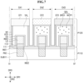
- the second display panel DP2 may include a semiconductor circuit board P110 and a light emitting element layer P120.
- the semiconductor circuit board P110 may include a first substrate SUB11, a plurality of pixel circuit units PXC, pixel electrodes 111, a first pad, a first common connection electrode of a common connection electrode, and a first insulating layer INS1.
- Each of the plurality of pixel circuits PXC may be disposed on the first substrate SUB 11.
- Each of the plurality of pixel circuit units PXC may include a complementary metal-oxide semiconductor ("CMOS") circuit formed using a semiconductor process.
- CMOS complementary metal-oxide semiconductor
- Each of the plurality of pixel circuit units PXC may include at least one transistor formed by the semiconductor process. Further, each of the plurality of pixel circuit units PXC may further include at least one capacitor formed by the semiconductor process.
- Each of the pixel electrodes 111 may be disposed on the corresponding pixel circuit unit PXC.
- Each of the pixel electrodes 111 may be an exposed electrode exposed from the pixel circuit unit PXC. That is, each of the pixel electrodes 111 may protrude from the top surface of the pixel circuit unit PXC.
- Each of the pixel electrodes 111 may be integrally formed with the pixel circuit unit PXC.
- Each of the pixel electrodes 111 may be supplied with a pixel voltage or an anode voltage from the pixel circuit unit PXC.
- the pixel electrodes 111 may include aluminum (Al).
- Each of the light emitting elements LE may be disposed on the connection electrode 112.
- the light emitting element LE may be a vertical light emitting diode element elongated in the third direction DR3. That is, the length of the light emitting element LE in the third direction DR3 may be longer than the length thereof in the horizontal direction.
- the length in the horizontal direction indicates a length in the first direction DR1 or a length in the second direction DR2.
- the length of the light emitting element LE in the third direction DR3 may be approximately 1 to 5 ⁇ m.
- a light transmitting layer TPL may be disposed on the common electrode CE in each of the first emission areas EA1.
- the light transmitting layer TPL may overlap the light emitting element LE in the third direction DR3 in each of the first emission areas EA1.
- the light transmitting layer TPL may be disposed to completely cover the light emitting element LE in each of the first emission areas EA1.
- the wavelength conversion layer QDL may be disposed on the common electrode CE in each of the second emission areas EA2 and the third emission areas EA3.
- the wavelength conversion layer QDL may overlap the light emitting element LE in the third direction DR3 in each of the second emission areas EA2 and the third emission areas EA3.
- the wavelength conversion layer QDL may be disposed to completely cover the light emitting element LE in each of the second emission areas EA2 and the third emission areas EA3.
- the QD may include a core and a shell that overcoats the core.
- the core may be at least one of, for example, CdS, CdSe, CdTe, ZnS, ZnSe, ZnTe, GaN, GaP, GaAs, GaSb, AlN, AlP, AlAs, AlSb, InP, InAs, InSb, SiC, Ca, Se, In, P, Fe, Pt, Ni, Co, Al, Ag, Au, Cu, FePt, Fe 2 O 3 , Fe 3 O 4 , Si and Ge, but is not limited thereto.
- the wavelength conversion layer QDL may further include a scatterer for scattering the light of the light emitting element LE in random directions.
- the scatterer may include a metal oxide particle or an organic particle.
- the metal oxide may be titanium oxide (TiO 2 ), zirconium oxide (ZrO 2 ), silicon dioxide (SiO 2 ), aluminum oxide (Al 2 O 3 ), indium oxide (In 2 O 3 ), zinc oxide (ZnO), or tin oxide (SnO 2 ).
- the organic particle may include acrylic resin or urethane resin.
- the diameter of the scatterer may be several to several tens of nanometers.
- Each of the first color filters CF1 may be disposed on the light transmitting layer TPL in the first emission area EA1.
- Each of the first color filters CF1 may transmit the first light and absorb or block the second light and the third light.
- each of the first color filters CF1 may transmit light in a blue wavelength band and may absorb or block light in a green and a red wavelength band. Therefore, each of the first color filters CF1 may transmit the first light emitted from the light emitting element LE. That is, the first light emitted from the light emitting element LE in the first emission area EA1 is not converted by a separate wavelength conversion layer, and may penetrate the first color filter CF1 through the light transmitting layer TPL. Accordingly, each of the first emission areas EA1 may emit the first light.
- Each of the second color filters CF2 may be disposed on the wavelength conversion layer QDL in the second emission area EA2.
- Each of the second color filters CF2 may transmit the second light and absorb or block the first light and the third light.
- each of the second color filters CF2 may transmit light in a green wavelength band and absorb or block light in a blue and a red wavelength band. Therefore, each of the second color filters CF2 may absorb or block, among the first lights emitted from the light emitting element LE, the first light that is not converted by the wavelength conversion layer QDL.
- each of the second color filters CF2 may transmit the second light corresponding to the green wavelength band and absorb or block the third light corresponding to the blue wavelength band from the fourth light converted by the wavelength conversion layer QDL. Accordingly, each of the second emission areas EA1 may emit the second light.
- Each of the third color filters CF3 may be disposed on the wavelength conversion layer QDL in the third emission area EA3.
- Each of the third color filters CF3 may transmit the third light and absorb or block the first light and the second light.
- each of the third color filters CF3 may transmit light in a red wavelength band and absorb or block light in a blue and green wavelength band. Therefore, each of the third color filters CF3 may absorb or block, among the first lights emitted from the light emitting element LE, the first light that is not converted by the wavelength conversion layer QDL.
- each of the third color filters CF3 may transmit the third light corresponding to the red wavelength band and absorb or block the second light corresponding to the green wavelength band from the fourth light converted by the wavelength conversion layer QDL. Accordingly, each of the third emission areas EA3 may emit the third light.
- a black matrix may be disposed between the plurality of color filters CF1, CF2, and CF3.
- the black matrix may be disposed between the first color filter CF1 and the second color filter CF2, between the second color filter CF2 and the third color filter CF3, and between the first color filter CF1 and the third color filter CF3.
- the black matrix may include an inorganic black pigment such as carbon black or an organic black pigment.
- the wavelength conversion layer QDL may be disposed instead of the light transmitting layer TPL in each of the first emission areas EA1 in FIG. 5 .
- FIG. 8 is a front view illustrating a multi-channel lens disposed on the front surfaces of the display panel.
- FIGS. 9A and 9B are perspective views respectively illustrating one side and the other side of the multi-channel lens shown in FIG. 8 in detail.
- the first multi-channel lens LS1 may include the first sub-lens LS11, the second sub-lens LS12, the third sub-lens LS13, and the fourth sub-lens LS14.
- the second multi-channel lens LS2 may include the fifth sub-lens LS21, the sixth sub-lens LS22, the seventh sub-lens LS23, and the eighth sub-lens LS24.
- the number of the plurality of sub-lenses LS11, LS12, LS13, LS14, LS21, LS22, LS23, and LS24 is not limited thereto.
- the first multi-channel lens LS1 illustrated in FIG. 9 may have a substantially circular shape in a plan view.
- the first sub-lens LS11, the second sub-lens LS12, the third sub-lens LS13, and the fourth sub-lens LS14 may be disposed in, for example, a clover shape to surround the center of the circular shape of the first multi-channel lens LS1 in a plan view. For example, as illustrated in FIG.
- the first sub-lens LS11, the second sub-lens LS12, the third sub-lens LS13, and the fourth sub-lens LS14 may be disposed at an upper right end, an upper left end, a lower left end and a lower right end, respectively, with respect to the center of the first multi-channel lens LS1.
- the first sub-lens LS11, the second sub-lens LS12, the third sub-lens LS13, and the fourth sub-lens LS14 may be integrally connected to each other or may be separated from each other.
- FIG. 9A is a perspective view illustrating one side of the first multi-channel lens LS1 facing the user's eye.
- FIG. 9B is a perspective view illustrating the other side of the first multi-channel lens LS1 facing an image displaying surface of the display panel DP.
- the second multi-channel lens LS2 may have a substantially hemispherical cross-section
- the fifth sub-lens LS21, the sixth sub-lens LS22, the seventh sub-lens LS23, and the eighth sub-lens LS24 may be disposed in a circular shape or a clover shape surrounding the center of the second multi-channel lens LS2 in a plan view.
- first to fourth inner coating regions MI11, MI12, MI13, and MI14 facing the first to fourth mirror coating regions M11, M12, M13, and M14 are defined in the concave portion, which is the center of the first multi-channel lens LS1 and is the rear surface of the first multi-channel lens LS1.
- a reflective material is formed or coated on the first to fourth inner coating regions MI11, MI12, MI13, and MI14.
- the first to fourth inner coating regions MI11, MI12, MI13, and MI14 may reflect the image displaying light reflected from the first to fourth mirror coating regions M11, M12, M13, and M14 in the direction of the user's eye, which is the forward direction.
- FIG. 12 is a plan view and a cross-sectional view of the display unit taken along line B-B' of FIG. 8
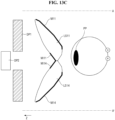
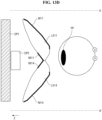
- FIG. 13A to FIG. 13D are cross-sectional views of the display unit taken along line A-A' of FIG. 8
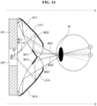
- FIG. 14 is a diagram illustrating the light emitted from FIG. 13A .
- FIG. 13A is a cross-sectional view illustrating an example in which the second display panel DP2 is embedded in the first display panel DP1, and FIGS. 13B to 13D illustrate modification examples of FIG. 13A , in which the second display panel DP2 may not be embedded in the first display panel DP1 but be arranged in a line with the first display panel DP1.
- the second display panel DP2 may be disposed on the rear surface of the first display panel DP1.
- the first display panel DP1 may define a through-hole formed in a region overlapping the second display panel DP2 in a thickness direction. Accordingly, the image of the first display panel DP1 and the image of the second display panel DP2 do not overlap each other in a thickness direction.
- the fourth sub-lens LS14 provides a channel through which the light IMG1' emitted from one area (e.g., a lower end of the display panel DP of FIG. 5 ) of the first sub-display panel DP1-1 and the light IMG2' emitted from one area of the third sub-display panel DP2-1 (e.g., a lower end of the display panel DP2 of FIG. 5 ) pass.
- the one area and the other area of the first sub-display panel DP1-1 may include an area overlapping the first sub-lens LS11 and an area overlapping the fourth sub-lens LS14, respectively.
- the second sub-lens L12 and the fourth sub-lens L14 may provide channels through which the lights emitted from different regions of the second sub-display panel DP1-2 and the fourth sub-display panel DP2-2 pass.
- the light IMG1 emitted from the first display panel DP1 is directed toward the peripheral vision that is the outside the foveal vision of the user's eye.
- the first display image corresponding to the peripheral vision is displayed by the first lights IMG1 and IMG1' emitted from the first display panel DP1
- the second display image corresponding to the foveal vision is displayed by the second lights IMG2 and IMG2' emitted from the first display panel DP1.
- the first display panel DP1 may further include a plurality of regions having different resolutions.
- a peripheral region of a predetermined area may be defined along the edge of the second display panel DP2.
- the peripheral region may have a lower resolution than the foveal vision and a higher resolution than the peripheral vision.
- FIG. 15 is an exploded perspective view of a display unit according to another modified example
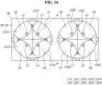
- FIG. 16 is a plan view of the display unit of FIG. 15
- FIG. 17 is a cross-sectional view taken along line A-A' of FIG. 16
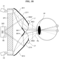
- FIG. 18 is a cross-sectional view illustrating the light emitted from the display unit of FIG. 17 .
- the third sub-display panel DP2-1 is disposed at the center of the rear surface of the first sub-display panel DP1-1
- the fourth sub-display panel DP2-2 is disposed at the center of the rear surface of the second sub-display panel DP1-2.
- the controller may control an operation of at least one of a plurality of infrared light sources (see L1, L2, L3, L4, L5, L6, L7, and L8 of FIG. 15 ) and the plurality of infrared cameras (see C1, C2, C3, C4, C5, C6, C7, and C8 of FIGS. 15 and 16 ).
- the controller may perform operations for the analysis of images obtained by the infrared cameras (see C1, C2, C3, C4, C5, C6, C7, and C8 of FIGS. 15 and 16 ), calculation of the position of the user's pupil PP, image processing (image mapping) based on those images, and display of the processed images on the display panel DP, and the like.
- the controller may be implemented as a dedicated processor including an embedded processor and/or a general-purpose processor including a central processing unit or an application processor, but is not limited thereto.
- the plurality of infrared light sources L1, L2, L3, L4, L5, L6, L7, and L8 may include the first infrared light source L1, the second infrared light source L2, the third infrared light source L3, the fourth infrared light source L4, the fifth infrared light source L5, the sixth infrared light source L6, the seventh infrared light source L7, and the eighth infrared light source L8.
- the first infrared light source L1, the second infrared light source L2, the third infrared light source L3, the fourth infrared light source L4, the fifth infrared light source L5, the sixth infrared light source L6, the seventh infrared light source L7, and the eighth infrared light source L8 may be disposed at the first sub-lens LS1 1, the second sub-lens L12, the third sub-lens L13, the fourth sub-lens LS14, the fifth sub-lens L21, the sixth sub-lens L22, the seventh sub-lens L23, and the eighth sub-lens L24, respectively.
- the first infrared camera C1, the second infrared camera C2, the third infrared camera C3, the fourth infrared camera C4, the fifth infrared camera C5, the sixth infrared camera C6, the seventh infrared camera C7, and the eighth infrared camera C8 may be disposed to overlap the first sub-lens LS11, the second sub-lens L12, the third sub-lens L13, the fourth sub-lens LS14, the fifth sub-lens L21, the sixth sub-lens L22, the seventh sub-lens L23, and the eighth sub-lens L24 in the thickness directions, respectively.
- the first infrared camera C1, the second infrared camera C2, the third infrared camera C3, and the fourth infrared camera C4 may overlap the boundary of the first multi-channel lens LS1 in the thickness direction (i.e., in a plan view).
- the fifth infrared camera C5, the sixth infrared camera C6, the seventh infrared camera C7, and the eighth infrared camera C8 may also be disposed in substantially the same or similar manner as the first infrared camera C1, the second infrared camera C2, and the fourth infrared camera C4, respectively, with respect to the second multi-channel lens LS2.
- Light steerers BD1 and BD2 may be interposed between the second display panel DP2 and the multi-channel lenses LS1 and LS2.
- the light steerers BD1 and BD2 may be interposed between the second display panel DP2 and the first display panel DP1.
- the light steerers BD1 and BD2 may be disposed to overlap the second display panel DP2 in the thickness direction.
- the second light steerer BD2 may be interposed between the fourth sub-display panel DP2-2 and the second multi-channel lens LS2.
- the second light steerer BD2 overlaps the fourth sub-display panel DP2-2.
- the second light steerer BD2 adjusts the direction of the light emitted from the fourth sub-display panel DP2-2.
- the second light steerer BD2 may be in contact with the fourth sub-display panel DP2-2, but is not limited thereto, and the second light steerer BD2 may be spaced apart from the fourth sub-display panel DP2-2.
- the second light steerer BD2 may have a circular shape to correspond to the shape of the fourth sub-display panel DP2-2.
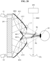
- the concave mirror CCL may be subjected to aspherical treatment to prevent distortion due to spherical aberration.
- the half mirror ML may be disposed between the multi-channel lens LS1 and the eyeball.
- the half mirror ML transmits the light emitted from the first display panel DP1.
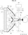
- one or more light magnification members may be disposed between the second display panel DP2 and the half mirror ML, as illustrated in FIG. 21 and FIG. 22 .
- the second display panel DP2 does not overlap the first display panel in the thickness direction. Accordingly, the sense of distance may be different between the second display image of the second display panel DP2 and the first display image of the first display panel DP1. In order to adjust this, one or more light magnification members may be disposed in the light traveling direction of the second display panel DP2.
- the light magnification member may be one or more of a convex lens CVL and a concave lens (not shown).
- the convex lens CVL may be further positioned between the second display panel DP2 and the half mirror ML.
- the convex lens CVL may perform a function of enlarging the light emitted from the second display panel DP2 at a predetermined magnification. Accordingly, the convex lens CVL adjusts the depth of the image of the second display panel DP2. A difference in the sense of depth between the first display panel DP1 and the second display panel DP2 may be adjusted.
- the convex lens CVL may perform a function of enlarging the light emitted from the second display panel DP2 at a predetermined magnification.
- FIG. 23 is a cross-sectional view for describing a ghost image display path of a display device and a cause thereof.
- the light emitted from the second display panel DP2 and incident on the half mirror ML is desirably transmitted to the concave mirror CCL. Further, the light emitted from the first display panel DP1 and incident on the half mirror ML is desirably transmitted to proceed in the direction of the eyeball. However, some of the light supposed to be transmitted through the half mirror ML in this way is reflected and incident on the multi-channel lens LS1. Referring to FIGS. 11 and 22 , when the light incident to the first multi-channel lens LS1 is reflected from the first to fourth mirror coating regions M11, M12, M13, and M14, unplanned light paths are formed and a ghost image is displayed.
- the position of the pupil may be tracked by the eye tracking unit 160. Since the eye tracking unit 160 is substantially the same as or similar to the eye tracking unit 160 described with reference to FIGS. 16 to 18 , redundant description thereof will be omitted.
- the processor adjusts the angle of the half mirror ML based on the position of the pupil detected by the eye tracking unit 160 so that the second display image of the second display panel DP2 corresponds to the foveal vision.
- the angle of the half mirror ML may be changed by an electromagnetic force, a piezoelectric force, or the like.
- a polarization control member may be further used to prevent an unplanned ghost image emitted from at least one of the first display panel DP1 or the second display panel DP2 and reflected from the half mirror ML.
- a reflective polarization film RPF may be attached to the reflective surface of the half mirror ML.
- a reflective polarizer RP may be disposed instead of the half mirror ML.
- phase delay element RT may be disposed in parallel with the half mirror ML.
- the phase delay element RT is disposed between the half mirror ML and the concave mirror CCL on the optical path of the second display panel DP2.
- the phase delay element RT may be a retarder.
- the ghost image may not be recognized by the user.
- FIG. 26 is a flowchart illustrating a display device control method according to one embodiment.
- a method of controlling the display device 1 may include a head mounted display control method.
- the method of controlling the display device 1 may be performed by the above-described controller.
- step S 110 the processor synchronizes an image signal inputted to the first display panel DP1 with an image signal inputted to the second display panel DP2.
- a reference image is first determined.
- the reference image is set to be an image inputted to the second display panel DP2, but is not limited thereto.
- an image inputted to the second display panel DP2, which is the reference image, and an image inputted to the first display panel DP1 may be synchronized.
- step S120 the processor generates a second display image of the second display panel DP2.
- the display image is an image displayed by the second display panel DP2, and may imply an image and/or a video recognized by the user.
- the processor separates an image corresponding to the foveal vision region from the entire image. The separated image corresponding to the foveal vision region becomes the second display image of the second display panel DP2.
- step S130 the second display panel DP2 displays the second display image, and the first display panel DP1 displays the entire image.
- the second display panel DP2 is embedded in the central region of the first display panel DP1, it is not necessary to cut out an area corresponding to the second display image from the entire image of the first display panel DP1.
- FIG. 27 is a flowchart of a display device control method according to another embodiment.
- FIG. 27 illustrates a method of controlling a display device including an eye tracking unit.
- the display device control method may include a head mounted display control method.
- the display device control method may be performed by the above-described controller.
- step S210 the eye tracking unit 160 detects the position of the user's pupil.
- the infrared ray reflected from the user's pupil PP may be received through the camera provided at the first display panel DP1, and the position of the user's pupil PP may be detected based on the received infrared ray.
- the position of the user's pupil PP may be detected by the plurality of infrared cameras C1, C2, C3, C4, C5, C6, C7, and C8 respectively disposed to overlap the transmission regions TR on the rear surface DP_RS of the first display panel DP1 to determine the gaze direction of the user.
- the infrared ray reflected from the user's pupil PP is not received by the first to fourth infrared cameras C1 to C4.
- the user's pupil PP may not be detected.
- the coordinates of the pupil PP of the user may be determined to be (0,0).
- the pupil PP of the user may be detected by at least one of the first to fourth infrared cameras C1 to C4.
- the user's pupil PP may be detected by the first infrared camera C1.
- the coordinates of the user's pupil PP may be determined to be located in a first quadrant P1_1 (e.g., (3, 1)).
- step S220 the processor synchronizes an image signal inputted to the first display panel DP1 with an image signal inputted to the second display panel DP2.
- a reference image is first determined.
- the reference image is set to be an image inputted to the second display panel DP2, but is not limited thereto.
- an image inputted to the second display panel DP2, which is the reference image, and an image inputted to the first display panel DP1 may be synchronized.
- step S230 the processor generates a second display image of the second display panel DP2 and a first display image of the first display panel DP1.
- the processor separates, from the entire image, an image corresponding to the foveal vision region based on the pupil position detected in step S210.
- the separated image corresponding to the foveal vision region becomes the second display image of the second display panel DP2, and the remaining image corresponding to the area other than the separated foveal vision region becomes the first display image of the first display panel DP1.
- blur processing may be performed on an edge generated by the separation of the foveal vision region in the first display image of the first display panel DP1.
- step S240 the second display panel DP2 displays the second display image in an area corresponding to the foveal vision, and the first display panel DP1 displays the first display image in an area corresponding to the peripheral vision.
- the method of controlling the display device 1 is not limited to the above-described example, and at least a part of the steps may be omitted, or at least one other step may be further included with reference to the other description of the present specification.
- NPs Numbered Paragraphs
Landscapes
- Physics & Mathematics (AREA)
- Engineering & Computer Science (AREA)
- General Physics & Mathematics (AREA)
- Optics & Photonics (AREA)
- Theoretical Computer Science (AREA)
- Computer Hardware Design (AREA)
- General Engineering & Computer Science (AREA)
- Human Computer Interaction (AREA)
- Multimedia (AREA)
- Signal Processing (AREA)
- Devices For Indicating Variable Information By Combining Individual Elements (AREA)
- Electroluminescent Light Sources (AREA)
- Liquid Crystal (AREA)
Applications Claiming Priority (1)
| Application Number | Priority Date | Filing Date | Title |
|---|---|---|---|
| KR1020220075077A KR20230174355A (ko) | 2022-06-20 | 2022-06-20 | 표시 장치 및 그 제어방법 |
Publications (2)
| Publication Number | Publication Date |
|---|---|
| EP4296747A2 true EP4296747A2 (de) | 2023-12-27 |
| EP4296747A3 EP4296747A3 (de) | 2024-04-17 |
Family
ID=86899326
Family Applications (1)
| Application Number | Title | Priority Date | Filing Date |
|---|---|---|---|
| EP23180167.1A Pending EP4296747A3 (de) | 2022-06-20 | 2023-06-19 | Anzeigevorrichtung und verfahren zur steuerung davon |
Country Status (4)
| Country | Link |
|---|---|
| US (1) | US12295242B2 (de) |
| EP (1) | EP4296747A3 (de) |
| KR (1) | KR20230174355A (de) |
| CN (1) | CN117270205A (de) |
Families Citing this family (2)
| Publication number | Priority date | Publication date | Assignee | Title |
|---|---|---|---|---|
| CN118661127A (zh) * | 2022-02-09 | 2024-09-17 | 株式会社半导体能源研究所 | 电子设备 |
| CN118135951B (zh) * | 2024-01-09 | 2024-09-06 | 天宜微电子(杭州)有限公司 | 显示驱动装置、显示装置及显示驱动方法 |
Family Cites Families (14)
| Publication number | Priority date | Publication date | Assignee | Title |
|---|---|---|---|---|
| KR101455714B1 (ko) | 2013-07-24 | 2014-11-03 | 한국과학기술연구원 | 헤드 마운티드 디스플레이 장치 및 이의 영상 왜곡 보정 방법 |
| KR102549397B1 (ko) | 2015-01-21 | 2023-06-28 | 테세랜드 엘엘씨 | 인간 눈 해상도에 조정된 이미징 광학 기기 |
| WO2017091477A1 (en) | 2015-11-25 | 2017-06-01 | Google Inc. | Prism-based eye tracking |
| US9779478B1 (en) | 2016-10-04 | 2017-10-03 | Oculus Vr, Llc | Rendering composite content on a head-mounted display including a high resolution inset |
| CN106940478A (zh) | 2017-04-24 | 2017-07-11 | 核桃智能科技(常州)有限公司 | 一种近眼显示系统以及带有该近眼显示系统的头戴设备 |
| US10768371B1 (en) | 2017-12-12 | 2020-09-08 | Facebook Technologies, Llc | Multiplexing optical assembly with a high resolution inset |
| US20200166752A1 (en) | 2018-11-26 | 2020-05-28 | Varjo Technologies Oy | Display for use in display apparatus |
| US10962795B1 (en) | 2018-12-17 | 2021-03-30 | Facebook Technologies, Llc | Display with a resolution enhanced region |
| WO2020205784A1 (en) | 2019-03-29 | 2020-10-08 | Avegant Corp. | Steerable hybrid display using a waveguide |
| CN112419986A (zh) | 2019-08-20 | 2021-02-26 | Oppo广东移动通信有限公司 | 头戴式显示设备的图像显示方法、装置及系统 |
| WO2021055256A1 (en) | 2019-09-17 | 2021-03-25 | Akalana Management Llc | Optical systems with lens-based static foveation |
| FR3107611B1 (fr) * | 2020-02-26 | 2022-03-04 | Aledia | Ecran d’affichage à résolution multiple et procédé de réalisation |
| KR102807770B1 (ko) | 2020-09-04 | 2025-05-15 | 삼성디스플레이 주식회사 | 라이트 필드 표시 장치 및 이의 영상 처리 방법 |
| CN214586228U (zh) | 2020-12-21 | 2021-11-02 | 歌尔光学科技有限公司 | 增强现实光学装置 |
-
2022
- 2022-06-20 KR KR1020220075077A patent/KR20230174355A/ko active Pending
-
2023
- 2023-04-11 US US18/132,968 patent/US12295242B2/en active Active
- 2023-06-19 EP EP23180167.1A patent/EP4296747A3/de active Pending
- 2023-06-19 CN CN202310726117.7A patent/CN117270205A/zh active Pending
Also Published As
| Publication number | Publication date |
|---|---|
| US20230413650A1 (en) | 2023-12-21 |
| EP4296747A3 (de) | 2024-04-17 |
| US12295242B2 (en) | 2025-05-06 |
| KR20230174355A (ko) | 2023-12-28 |
| CN117270205A (zh) | 2023-12-22 |
Similar Documents
| Publication | Publication Date | Title |
|---|---|---|
| US12057531B2 (en) | Display device | |
| KR102031648B1 (ko) | 유기 발광 표시 장치 | |
| KR102875162B1 (ko) | 표시 장치 | |
| JP5329882B2 (ja) | ディスプレイ装置 | |
| EP4296747A2 (de) | Anzeigevorrichtung und verfahren zur steuerung davon | |
| KR20240083222A (ko) | 영상 표시 모듈을 포함하는 웨어러블 장치 | |
| KR20200109438A (ko) | 가상 영상 표시장치 및 헤드 마운트 장치 | |
| KR102819956B1 (ko) | 표시 모듈과 이를 포함한 헤드 장착형 표시장치 | |
| KR102743905B1 (ko) | 표시 장치 | |
| CN114792709A (zh) | 显示面板、显示装置以及显示装置的控制方法 | |
| US12439796B2 (en) | Image display device and electronic apparatus | |
| CN119731574A (zh) | 用于vr头戴式视图器的透明微led显示器 | |
| CN115274937A (zh) | 用于制造显示装置的设备和方法 | |
| US9859527B2 (en) | Reflective layer for increasing fill factor in an electronic display | |
| KR102950782B1 (ko) | 표시 패널 및 전자 기기 | |
| US12586247B2 (en) | Image distortion calibration device, display device and distortion calibration method | |
| US11789270B2 (en) | Optical device | |
| JP2023026092A (ja) | 発光装置、光電変換装置、電子機器、照明装置および移動体 | |
| US12270998B2 (en) | Display device and method of controlling the same | |
| US12579915B2 (en) | Image display device and electronic device including pixels in respective light emitting regions with differently sized light-emitting areas | |
| JP2022047608A (ja) | 有機発光装置、表示装置、光電変換装置、電子機器、照明装置、および移動体 | |
| US11997250B2 (en) | Device for providing augmented reality and system for providing augmented reality using the same | |
| KR102717300B1 (ko) | 헤드 장착형 디스플레이 | |
| US20260090206A1 (en) | Display device | |
| US20260013380A1 (en) | Display device including doublet lens |
Legal Events
| Date | Code | Title | Description |
|---|---|---|---|
| PUAI | Public reference made under article 153(3) epc to a published international application that has entered the european phase |
Free format text: ORIGINAL CODE: 0009012 |
|
| STAA | Information on the status of an ep patent application or granted ep patent |
Free format text: STATUS: THE APPLICATION HAS BEEN PUBLISHED |
|
| AK | Designated contracting states |
Kind code of ref document: A2 Designated state(s): AL AT BE BG CH CY CZ DE DK EE ES FI FR GB GR HR HU IE IS IT LI LT LU LV MC ME MK MT NL NO PL PT RO RS SE SI SK SM TR |
|
| PUAL | Search report despatched |
Free format text: ORIGINAL CODE: 0009013 |
|
| AK | Designated contracting states |
Kind code of ref document: A3 Designated state(s): AL AT BE BG CH CY CZ DE DK EE ES FI FR GB GR HR HU IE IS IT LI LT LU LV MC ME MK MT NL NO PL PT RO RS SE SI SK SM TR |
|
| RIC1 | Information provided on ipc code assigned before grant |
Ipc: G02B 27/28 20060101ALI20240311BHEP Ipc: G02B 27/01 20060101ALI20240311BHEP Ipc: G02B 25/00 20060101ALI20240311BHEP Ipc: G02B 17/08 20060101AFI20240311BHEP |
|
| STAA | Information on the status of an ep patent application or granted ep patent |
Free format text: STATUS: REQUEST FOR EXAMINATION WAS MADE |
|
| 17P | Request for examination filed |
Effective date: 20241015 |
|
| RBV | Designated contracting states (corrected) |
Designated state(s): AL AT BE BG CH CY CZ DE DK EE ES FI FR GB GR HR HU IE IS IT LI LT LU LV MC ME MK MT NL NO PL PT RO RS SE SI SK SM TR |
|
| STAA | Information on the status of an ep patent application or granted ep patent |
Free format text: STATUS: EXAMINATION IS IN PROGRESS |
|
| 17Q | First examination report despatched |
Effective date: 20260123 |
|
| P01 | Opt-out of the competence of the unified patent court (upc) registered |
Free format text: CASE NUMBER: UPC_APP_0007134_4296747/2026 Effective date: 20260226 |