EP4292743A1 - Circuit board and manufacturing method - Google Patents
Circuit board and manufacturing method Download PDFInfo
- Publication number
- EP4292743A1 EP4292743A1 EP22752596.1A EP22752596A EP4292743A1 EP 4292743 A1 EP4292743 A1 EP 4292743A1 EP 22752596 A EP22752596 A EP 22752596A EP 4292743 A1 EP4292743 A1 EP 4292743A1
- Authority
- EP
- European Patent Office
- Prior art keywords
- engagement
- tool
- metal layer
- uneven portion
- circuit board
- Prior art date
- Legal status (The legal status is an assumption and is not a legal conclusion. Google has not performed a legal analysis and makes no representation as to the accuracy of the status listed.)
- Pending
Links
Images





Classifications
-
- H—ELECTRICITY
- H05—ELECTRIC TECHNIQUES NOT OTHERWISE PROVIDED FOR
- H05K—PRINTED CIRCUITS; CASINGS OR CONSTRUCTIONAL DETAILS OF ELECTRIC APPARATUS; MANUFACTURE OF ASSEMBLAGES OF ELECTRICAL COMPONENTS
- H05K1/00—Printed circuits
- H05K1/18—Printed circuits structurally associated with non-printed electric components
- H05K1/182—Printed circuits structurally associated with non-printed electric components associated with components mounted in printed circuit boards [PCB], e.g. insert-mounted components [IMC]
- H05K1/183—Printed circuits structurally associated with non-printed electric components associated with components mounted in printed circuit boards [PCB], e.g. insert-mounted components [IMC] associated with components mounted in and supported by recessed areas of the PCBs
-
- B—PERFORMING OPERATIONS; TRANSPORTING
- B23—MACHINE TOOLS; METAL-WORKING NOT OTHERWISE PROVIDED FOR
- B23K—SOLDERING OR UNSOLDERING; WELDING; CLADDING OR PLATING BY SOLDERING OR WELDING; CUTTING BY APPLYING HEAT LOCALLY, e.g. FLAME CUTTING; WORKING BY LASER BEAM
- B23K1/00—Soldering, e.g. brazing, or unsoldering
- B23K1/20—Preliminary treatment of work or areas to be soldered, e.g. in respect of a galvanic coating
-
- B—PERFORMING OPERATIONS; TRANSPORTING
- B23—MACHINE TOOLS; METAL-WORKING NOT OTHERWISE PROVIDED FOR
- B23K—SOLDERING OR UNSOLDERING; WELDING; CLADDING OR PLATING BY SOLDERING OR WELDING; CUTTING BY APPLYING HEAT LOCALLY, e.g. FLAME CUTTING; WORKING BY LASER BEAM
- B23K1/00—Soldering, e.g. brazing, or unsoldering
- B23K1/0008—Soldering, e.g. brazing, or unsoldering specially adapted for particular articles or work
- B23K1/0016—Soldering of electronic components
-
- B—PERFORMING OPERATIONS; TRANSPORTING
- B23—MACHINE TOOLS; METAL-WORKING NOT OTHERWISE PROVIDED FOR
- B23K—SOLDERING OR UNSOLDERING; WELDING; CLADDING OR PLATING BY SOLDERING OR WELDING; CUTTING BY APPLYING HEAT LOCALLY, e.g. FLAME CUTTING; WORKING BY LASER BEAM
- B23K20/00—Non-electric welding by applying impact or other pressure, with or without the application of heat, e.g. cladding or plating
- B23K20/10—Non-electric welding by applying impact or other pressure, with or without the application of heat, e.g. cladding or plating making use of vibrations, e.g. ultrasonic welding
-
- H—ELECTRICITY
- H05—ELECTRIC TECHNIQUES NOT OTHERWISE PROVIDED FOR
- H05K—PRINTED CIRCUITS; CASINGS OR CONSTRUCTIONAL DETAILS OF ELECTRIC APPARATUS; MANUFACTURE OF ASSEMBLAGES OF ELECTRICAL COMPONENTS
- H05K1/00—Printed circuits
- H05K1/02—Details
- H05K1/0201—Thermal arrangements, e.g. for cooling, heating or preventing overheating
- H05K1/0203—Cooling of mounted components
- H05K1/0209—External configuration of printed circuit board adapted for heat dissipation, e.g. lay-out of conductors, coatings
-
- H—ELECTRICITY
- H05—ELECTRIC TECHNIQUES NOT OTHERWISE PROVIDED FOR
- H05K—PRINTED CIRCUITS; CASINGS OR CONSTRUCTIONAL DETAILS OF ELECTRIC APPARATUS; MANUFACTURE OF ASSEMBLAGES OF ELECTRICAL COMPONENTS
- H05K1/00—Printed circuits
- H05K1/18—Printed circuits structurally associated with non-printed electric components
- H05K1/182—Printed circuits structurally associated with non-printed electric components associated with components mounted in printed circuit boards [PCB], e.g. insert-mounted components [IMC]
- H05K1/185—Printed circuits structurally associated with non-printed electric components associated with components mounted in printed circuit boards [PCB], e.g. insert-mounted components [IMC] associated with components encapsulated in the insulating substrate of the PCBs; associated with components incorporated in internal layers of multilayer circuit boards
- H05K1/186—Printed circuits structurally associated with non-printed electric components associated with components mounted in printed circuit boards [PCB], e.g. insert-mounted components [IMC] associated with components encapsulated in the insulating substrate of the PCBs; associated with components incorporated in internal layers of multilayer circuit boards manufactured by mounting on or connecting to patterned circuits before or during embedding
-
- H—ELECTRICITY
- H05—ELECTRIC TECHNIQUES NOT OTHERWISE PROVIDED FOR
- H05K—PRINTED CIRCUITS; CASINGS OR CONSTRUCTIONAL DETAILS OF ELECTRIC APPARATUS; MANUFACTURE OF ASSEMBLAGES OF ELECTRICAL COMPONENTS
- H05K3/00—Apparatus or processes for manufacturing printed circuits
- H05K3/0058—Laminating printed circuit boards onto other substrates, e.g. metallic substrates
- H05K3/0061—Laminating printed circuit boards onto other substrates, e.g. metallic substrates onto a metallic substrate, e.g. a heat sink
-
- H—ELECTRICITY
- H05—ELECTRIC TECHNIQUES NOT OTHERWISE PROVIDED FOR
- H05K—PRINTED CIRCUITS; CASINGS OR CONSTRUCTIONAL DETAILS OF ELECTRIC APPARATUS; MANUFACTURE OF ASSEMBLAGES OF ELECTRICAL COMPONENTS
- H05K3/00—Apparatus or processes for manufacturing printed circuits
- H05K3/22—Secondary treatment of printed circuits
- H05K3/24—Reinforcing of the conductive pattern
-
- H—ELECTRICITY
- H05—ELECTRIC TECHNIQUES NOT OTHERWISE PROVIDED FOR
- H05K—PRINTED CIRCUITS; CASINGS OR CONSTRUCTIONAL DETAILS OF ELECTRIC APPARATUS; MANUFACTURE OF ASSEMBLAGES OF ELECTRICAL COMPONENTS
- H05K3/00—Apparatus or processes for manufacturing printed circuits
- H05K3/30—Assembling printed circuits with electric components, e.g. with resistors
- H05K3/32—Assembling printed circuits with electric components, e.g. with resistors electrically connecting electric components or wires to printed circuits
- H05K3/34—Assembling printed circuits with electric components, e.g. with resistors electrically connecting electric components or wires to printed circuits by soldering
- H05K3/346—Solder materials or compositions specially adapted therefor
-
- H—ELECTRICITY
- H10—SEMICONDUCTOR DEVICES; ELECTRIC SOLID-STATE DEVICES NOT OTHERWISE PROVIDED FOR
- H10W—GENERIC PACKAGES, INTERCONNECTIONS, CONNECTORS OR OTHER CONSTRUCTIONAL DETAILS OF DEVICES COVERED BY CLASS H10
- H10W70/00—Package substrates; Interposers; Redistribution layers [RDL]
- H10W70/60—Insulating or insulated package substrates; Interposers; Redistribution layers
-
- B—PERFORMING OPERATIONS; TRANSPORTING
- B23—MACHINE TOOLS; METAL-WORKING NOT OTHERWISE PROVIDED FOR
- B23K—SOLDERING OR UNSOLDERING; WELDING; CLADDING OR PLATING BY SOLDERING OR WELDING; CUTTING BY APPLYING HEAT LOCALLY, e.g. FLAME CUTTING; WORKING BY LASER BEAM
- B23K2101/00—Articles made by soldering, welding or cutting
- B23K2101/36—Electric or electronic devices
- B23K2101/42—Printed circuits
-
- H—ELECTRICITY
- H05—ELECTRIC TECHNIQUES NOT OTHERWISE PROVIDED FOR
- H05K—PRINTED CIRCUITS; CASINGS OR CONSTRUCTIONAL DETAILS OF ELECTRIC APPARATUS; MANUFACTURE OF ASSEMBLAGES OF ELECTRICAL COMPONENTS
- H05K1/00—Printed circuits
- H05K1/18—Printed circuits structurally associated with non-printed electric components
- H05K1/181—Printed circuits structurally associated with non-printed electric components associated with surface mounted components
-
- H—ELECTRICITY
- H05—ELECTRIC TECHNIQUES NOT OTHERWISE PROVIDED FOR
- H05K—PRINTED CIRCUITS; CASINGS OR CONSTRUCTIONAL DETAILS OF ELECTRIC APPARATUS; MANUFACTURE OF ASSEMBLAGES OF ELECTRICAL COMPONENTS
- H05K1/00—Printed circuits
- H05K1/18—Printed circuits structurally associated with non-printed electric components
- H05K1/182—Printed circuits structurally associated with non-printed electric components associated with components mounted in printed circuit boards [PCB], e.g. insert-mounted components [IMC]
- H05K1/185—Printed circuits structurally associated with non-printed electric components associated with components mounted in printed circuit boards [PCB], e.g. insert-mounted components [IMC] associated with components encapsulated in the insulating substrate of the PCBs; associated with components incorporated in internal layers of multilayer circuit boards
- H05K1/188—Printed circuits structurally associated with non-printed electric components associated with components mounted in printed circuit boards [PCB], e.g. insert-mounted components [IMC] associated with components encapsulated in the insulating substrate of the PCBs; associated with components incorporated in internal layers of multilayer circuit boards manufactured by mounting on or attaching to a structure having a conductive layer, e.g. a metal foil, such that the terminals of the component are connected to or adjacent to the conductive layer before embedding, and by using the conductive layer, which is patterned after embedding, at least partially for connecting the component
-
- H—ELECTRICITY
- H05—ELECTRIC TECHNIQUES NOT OTHERWISE PROVIDED FOR
- H05K—PRINTED CIRCUITS; CASINGS OR CONSTRUCTIONAL DETAILS OF ELECTRIC APPARATUS; MANUFACTURE OF ASSEMBLAGES OF ELECTRICAL COMPONENTS
- H05K2201/00—Indexing scheme relating to printed circuits covered by H05K1/00
- H05K2201/03—Conductive materials
- H05K2201/0332—Structure of the conductor
- H05K2201/0364—Conductor shape
- H05K2201/0373—Conductors having a fine structure, e.g. providing a plurality of contact points with a structured tool
-
- H—ELECTRICITY
- H05—ELECTRIC TECHNIQUES NOT OTHERWISE PROVIDED FOR
- H05K—PRINTED CIRCUITS; CASINGS OR CONSTRUCTIONAL DETAILS OF ELECTRIC APPARATUS; MANUFACTURE OF ASSEMBLAGES OF ELECTRICAL COMPONENTS
- H05K2201/00—Indexing scheme relating to printed circuits covered by H05K1/00
- H05K2201/06—Thermal details
- H05K2201/066—Heatsink mounted on the surface of the printed circuit board [PCB]
-
- H—ELECTRICITY
- H05—ELECTRIC TECHNIQUES NOT OTHERWISE PROVIDED FOR
- H05K—PRINTED CIRCUITS; CASINGS OR CONSTRUCTIONAL DETAILS OF ELECTRIC APPARATUS; MANUFACTURE OF ASSEMBLAGES OF ELECTRICAL COMPONENTS
- H05K2201/00—Indexing scheme relating to printed circuits covered by H05K1/00
- H05K2201/09—Shape and layout
- H05K2201/09209—Shape and layout details of conductors
- H05K2201/09654—Shape and layout details of conductors covering at least two types of conductors provided for in H05K2201/09218 - H05K2201/095
- H05K2201/09745—Recess in conductor, e.g. in pad or in metallic substrate
-
- H—ELECTRICITY
- H05—ELECTRIC TECHNIQUES NOT OTHERWISE PROVIDED FOR
- H05K—PRINTED CIRCUITS; CASINGS OR CONSTRUCTIONAL DETAILS OF ELECTRIC APPARATUS; MANUFACTURE OF ASSEMBLAGES OF ELECTRICAL COMPONENTS
- H05K2201/00—Indexing scheme relating to printed circuits covered by H05K1/00
- H05K2201/10—Details of components or other objects attached to or integrated in a printed circuit board
- H05K2201/10431—Details of mounted components
- H05K2201/10553—Component over metal, i.e. metal plate in between bottom of component and surface of PCB
-
- H—ELECTRICITY
- H05—ELECTRIC TECHNIQUES NOT OTHERWISE PROVIDED FOR
- H05K—PRINTED CIRCUITS; CASINGS OR CONSTRUCTIONAL DETAILS OF ELECTRIC APPARATUS; MANUFACTURE OF ASSEMBLAGES OF ELECTRICAL COMPONENTS
- H05K2201/00—Indexing scheme relating to printed circuits covered by H05K1/00
- H05K2201/10—Details of components or other objects attached to or integrated in a printed circuit board
- H05K2201/10431—Details of mounted components
- H05K2201/10598—Means for fastening a component, a casing or a heat sink whereby a pressure is exerted on the component towards the PCB
-
- H—ELECTRICITY
- H05—ELECTRIC TECHNIQUES NOT OTHERWISE PROVIDED FOR
- H05K—PRINTED CIRCUITS; CASINGS OR CONSTRUCTIONAL DETAILS OF ELECTRIC APPARATUS; MANUFACTURE OF ASSEMBLAGES OF ELECTRICAL COMPONENTS
- H05K2201/00—Indexing scheme relating to printed circuits covered by H05K1/00
- H05K2201/10—Details of components or other objects attached to or integrated in a printed circuit board
- H05K2201/10613—Details of electrical connections of non-printed components, e.g. special leads
- H05K2201/10954—Other details of electrical connections
- H05K2201/10969—Metallic case or integral heatsink of component electrically connected to a pad on PCB
-
- H—ELECTRICITY
- H05—ELECTRIC TECHNIQUES NOT OTHERWISE PROVIDED FOR
- H05K—PRINTED CIRCUITS; CASINGS OR CONSTRUCTIONAL DETAILS OF ELECTRIC APPARATUS; MANUFACTURE OF ASSEMBLAGES OF ELECTRICAL COMPONENTS
- H05K2201/00—Indexing scheme relating to printed circuits covered by H05K1/00
- H05K2201/20—Details of printed circuits not provided for in H05K2201/01 - H05K2201/10
- H05K2201/2072—Anchoring, i.e. one structure gripping into another
-
- H—ELECTRICITY
- H05—ELECTRIC TECHNIQUES NOT OTHERWISE PROVIDED FOR
- H05K—PRINTED CIRCUITS; CASINGS OR CONSTRUCTIONAL DETAILS OF ELECTRIC APPARATUS; MANUFACTURE OF ASSEMBLAGES OF ELECTRICAL COMPONENTS
- H05K2203/00—Indexing scheme relating to apparatus or processes for manufacturing printed circuits covered by H05K3/00
- H05K2203/02—Details related to mechanical or acoustic processing, e.g. drilling, punching, cutting, using ultrasound
- H05K2203/0285—Using ultrasound, e.g. for cleaning, soldering or wet treatment
-
- H—ELECTRICITY
- H05—ELECTRIC TECHNIQUES NOT OTHERWISE PROVIDED FOR
- H05K—PRINTED CIRCUITS; CASINGS OR CONSTRUCTIONAL DETAILS OF ELECTRIC APPARATUS; MANUFACTURE OF ASSEMBLAGES OF ELECTRICAL COMPONENTS
- H05K2203/00—Indexing scheme relating to apparatus or processes for manufacturing printed circuits covered by H05K3/00
- H05K2203/02—Details related to mechanical or acoustic processing, e.g. drilling, punching, cutting, using ultrasound
- H05K2203/0292—Using vibration, e.g. during soldering or screen printing
-
- H—ELECTRICITY
- H05—ELECTRIC TECHNIQUES NOT OTHERWISE PROVIDED FOR
- H05K—PRINTED CIRCUITS; CASINGS OR CONSTRUCTIONAL DETAILS OF ELECTRIC APPARATUS; MANUFACTURE OF ASSEMBLAGES OF ELECTRICAL COMPONENTS
- H05K2203/00—Indexing scheme relating to apparatus or processes for manufacturing printed circuits covered by H05K3/00
- H05K2203/03—Metal processing
- H05K2203/0307—Providing micro- or nanometer scale roughness on a metal surface, e.g. by plating of nodules or dendrites
-
- H—ELECTRICITY
- H10—SEMICONDUCTOR DEVICES; ELECTRIC SOLID-STATE DEVICES NOT OTHERWISE PROVIDED FOR
- H10W—GENERIC PACKAGES, INTERCONNECTIONS, CONNECTORS OR OTHER CONSTRUCTIONAL DETAILS OF DEVICES COVERED BY CLASS H10
- H10W40/00—Arrangements for thermal protection or thermal control
- H10W40/20—Arrangements for cooling
- H10W40/25—Arrangements for cooling characterised by their materials
- H10W40/251—Organics
-
- H—ELECTRICITY
- H10—SEMICONDUCTOR DEVICES; ELECTRIC SOLID-STATE DEVICES NOT OTHERWISE PROVIDED FOR
- H10W—GENERIC PACKAGES, INTERCONNECTIONS, CONNECTORS OR OTHER CONSTRUCTIONAL DETAILS OF DEVICES COVERED BY CLASS H10
- H10W40/00—Arrangements for thermal protection or thermal control
- H10W40/20—Arrangements for cooling
- H10W40/25—Arrangements for cooling characterised by their materials
- H10W40/255—Arrangements for cooling characterised by their materials having a laminate or multilayered structure, e.g. direct bond copper [DBC] ceramic substrates
-
- H—ELECTRICITY
- H10—SEMICONDUCTOR DEVICES; ELECTRIC SOLID-STATE DEVICES NOT OTHERWISE PROVIDED FOR
- H10W—GENERIC PACKAGES, INTERCONNECTIONS, CONNECTORS OR OTHER CONSTRUCTIONAL DETAILS OF DEVICES COVERED BY CLASS H10
- H10W72/00—Interconnections or connectors in packages
- H10W72/071—Connecting or disconnecting
- H10W72/0711—Apparatus therefor
- H10W72/07141—Means for applying energy, e.g. ovens or lasers
-
- H—ELECTRICITY
- H10—SEMICONDUCTOR DEVICES; ELECTRIC SOLID-STATE DEVICES NOT OTHERWISE PROVIDED FOR
- H10W—GENERIC PACKAGES, INTERCONNECTIONS, CONNECTORS OR OTHER CONSTRUCTIONAL DETAILS OF DEVICES COVERED BY CLASS H10
- H10W72/00—Interconnections or connectors in packages
- H10W72/071—Connecting or disconnecting
- H10W72/073—Connecting or disconnecting of die-attach connectors
- H10W72/07331—Connecting techniques
- H10W72/07332—Compression bonding, e.g. thermocompression bonding
- H10W72/07333—Ultrasonic bonding, e.g. thermosonic bonding
-
- H—ELECTRICITY
- H10—SEMICONDUCTOR DEVICES; ELECTRIC SOLID-STATE DEVICES NOT OTHERWISE PROVIDED FOR
- H10W—GENERIC PACKAGES, INTERCONNECTIONS, CONNECTORS OR OTHER CONSTRUCTIONAL DETAILS OF DEVICES COVERED BY CLASS H10
- H10W72/00—Interconnections or connectors in packages
- H10W72/30—Die-attach connectors
- H10W72/381—Auxiliary members
- H10W72/387—Flow barriers
-
- H—ELECTRICITY
- H10—SEMICONDUCTOR DEVICES; ELECTRIC SOLID-STATE DEVICES NOT OTHERWISE PROVIDED FOR
- H10W—GENERIC PACKAGES, INTERCONNECTIONS, CONNECTORS OR OTHER CONSTRUCTIONAL DETAILS OF DEVICES COVERED BY CLASS H10
- H10W72/00—Interconnections or connectors in packages
- H10W72/90—Bond pads, in general
- H10W72/921—Structures or relative sizes of bond pads
- H10W72/923—Bond pads having multiple stacked layers
-
- H—ELECTRICITY
- H10—SEMICONDUCTOR DEVICES; ELECTRIC SOLID-STATE DEVICES NOT OTHERWISE PROVIDED FOR
- H10W—GENERIC PACKAGES, INTERCONNECTIONS, CONNECTORS OR OTHER CONSTRUCTIONAL DETAILS OF DEVICES COVERED BY CLASS H10
- H10W72/00—Interconnections or connectors in packages
- H10W72/90—Bond pads, in general
- H10W72/931—Shapes of bond pads
-
- H—ELECTRICITY
- H10—SEMICONDUCTOR DEVICES; ELECTRIC SOLID-STATE DEVICES NOT OTHERWISE PROVIDED FOR
- H10W—GENERIC PACKAGES, INTERCONNECTIONS, CONNECTORS OR OTHER CONSTRUCTIONAL DETAILS OF DEVICES COVERED BY CLASS H10
- H10W72/00—Interconnections or connectors in packages
- H10W72/90—Bond pads, in general
- H10W72/931—Shapes of bond pads
- H10W72/932—Plan-view shape, i.e. in top view
-
- H—ELECTRICITY
- H10—SEMICONDUCTOR DEVICES; ELECTRIC SOLID-STATE DEVICES NOT OTHERWISE PROVIDED FOR
- H10W—GENERIC PACKAGES, INTERCONNECTIONS, CONNECTORS OR OTHER CONSTRUCTIONAL DETAILS OF DEVICES COVERED BY CLASS H10
- H10W90/00—Package configurations
- H10W90/701—Package configurations characterised by the relative positions of pads or connectors relative to package parts
- H10W90/731—Package configurations characterised by the relative positions of pads or connectors relative to package parts of die-attach connectors
- H10W90/734—Package configurations characterised by the relative positions of pads or connectors relative to package parts of die-attach connectors between a chip and a stacked insulating package substrate, interposer or RDL
Definitions
- the present invention relates to a circuit board and a manufacturing method used for manufacturing the same.
- Patent document 1 There is one disclosed in Patent document 1 as a conventional circuit board.
- a circuit pattern of the circuit board is formed by wet etching conducted to a cupper foil (Cu foil) or an aluminum foil (Al foil).
- the Cu foil is made thick to effectively dissipate heat of electronic components such as semiconductor chip mounted on the circuit pattern. If the Cu foil is made thick, processing time for the etching is elongated to also deteriorate dimensional accuracy of the circuit pattern.
- a stacked circuit pattern is formed by a cold spray method on a circuit pattern formed by etching conducted to a Cu foil.
- the circuit board increase heat dissipation according to the stacking that makes the circuit pattern partly thick while suppressing processing time for the etching.
- the cold spray method is, however, a technique to form a coat by colliding particles of thermal spray material in a solid phase with a base material at high speed. Accordingly, large residual stress and thermal stress tend to be generated in a Cu layer of the stacked circuit pattern, and there is concern over a curve of the board. Further, powder is used for raw material to increase the cost.
- an ultrasonic bonding technique disclosed in Patent document 3 may be diverted to stack and bond a metal layer such as additional Cu foil on a circuit pattern such as a Cu foil.
- the bonding technique is to add ultrasonic vibration in a planar direction of an interface against a circuit pattern while pressing an electrode terminal using an ultrasonic horn, to bond the electrode terminal to the circuit pattern according to the ultrasonic vibration.
- ultrasonic vibration is added in a planar direction of an interface while pressing the additional metal layer using the ultrasonic horn, to bond the metal layer to the circuit pattern.
- Tool marks are, however, left by the pressing of the ultrasonic horn on a surface of the additional metal layer including a mounting surface for an electronic component. Accordingly, mounting an electronic component on the additional metal layer using solder, the solder with low heat conductivity is accumulated and additionally stayed in the tool marks to limit improvement of heat dissipation of the electronic component.
- a problem to be solved is that, if an additional metal layer is bonded to a circuit pattern by ultrasonic bonding and an electronic component is mounted on the additional metal layer using solder, it limits improvement of heat dissipation of the electronic component.
- a circuit board according to the present invention is a circuit board comprising a circuit pattern on a base plate and an additional metal layer layered and bonded on the circuit pattern, wherein the additional metal layer comprises an attachment plane portion configured to fix an electronic component using solder, and an engagement uneven portion provided adjacent to the attachment plane portion to be engaged with a tool uneven portion of a tool for vibration transmission to bond the additional metal layer on the circuit pattern with ultrasonic vibration, wherein the attachment plane portion is a face having unevenness smaller than the engagement uneven portion.
- a manufacturing method for the circuit board according to the present invention layers the additional metal layer on the circuit pattern, and presses a tool onto a surface of the additional metal layer to apply ultrasonic vibration, the tool having a retracted portion and a tool uneven portion corresponding to the attachment plane portion and the engagement uneven portion, thereby bonding the additional metal layer on the circuit pattern due to transmission of the ultrasonic vibration while leaving the attachment plane portion on the surface of the additional metal layer in an area according to the retracted portion and forming the engagement uneven portion on the surface of the additional metal layer according to the tool uneven portion.
- the circuit board according to the present invention layers and bonds the additional metal layer onto the circuit pattern, so that heat dissipation of an electronic component is improved according to increase of thickness of the metal layer, the electronic component fixed to the attachment plane portion of the additional metal layer using solder.
- Bonding of the additional metal layer is surely performed by transmitting the ultrasonic vibration in a planar direction using the tool in a state that the tool uneven portion engages with the engagement uneven portion of the metal layer.
- the engagement uneven portion adjacent to the attachment plane portion suppresses outflow of solder when an electronic component is fixed to the attachment plane portion of the additional metal layer.
- the manufacturing method of the circuit board according to the present invention allows outflow of solder fixing an electronic component to be suppressed using the engagement uneven portion having been used when performing bonding by ultrasonic vibration while providing the surface of the additional metal layer with the attachment plane portion.
- the tool used for the manufacturing method of the circuit board according to the present invention easily realizes the manufacturing method of the circuit board.
- the present invention accomplishes an object to further improve heat dissipation of a semiconductor chip mounted on an additional metal layer using solder, the additional metal layer bonded to a circuit pattern diverting an ultrasonic bonding technique as follows.
- a circuit board of the present invention comprises a circuit pattern (3) on a base plate (5) and an additional metal layer (9) layered and bonded on the circuit pattern (3).
- the additional metal layer (9) comprises an attachment plane portion (13) configured to fix an electronic component (11) using solder, and an engagement uneven portion (17) provided adjacent to the attachment plane portion (13) to be engaged with a tool uneven portion (15) of a tool (T) for vibration transmission to bond the additional metal layer (9) on the circuit pattern (3) with ultrasonic vibration.
- the attachment plane portion (13) is a face having unevenness smaller than the engagement uneven portion (17).
- attachment plane portion (13) should be the face having unevenness smaller than the engagement uneven portion (17), and the attachment plane portion may be a flat surface or an uneven surface having recesses and projections smaller than the engagement uneven portion.
- the engagement uneven portion (17) may be embodied by having engagement projected portions (17b) projecting from the attachment plane portion (13).
- the unevenness of the engagement uneven portion (17) is, however, relative, and the engagement uneven portion may be embodied by having the engagement projected portions (17b) having a height flushing with the attachment plane portion (13) or having a lower projection portions (17b) than the attachment plane portion (13).
- the engagement projected portions (17b) projecting from the attachment plane portion (13) may be embodied by bulging from the attachment plane portion (13) by plastically deforming the additional metal layer (9).
- the engagement projected portion (17b) may be embodied by having a recess (17c) or a flat face (17d) on a top. Further, the engagement uneven portion (17) may be embodied by having tilted side faces (17e).
- the engagement uneven portion (17) is indentation of the tool uneven portion (15).
- the engagement uneven portion (17) may be formed by pressing of a special tool separated from the tool (T) for transmitting ultrasonic vibration.
- the engagement uneven portion (17) may be formed on the additional metal layer (9) by cutting, a laser or the like.
- the engagement uneven portion (17) and the tool uneven portion (15) may correspond one to one in a case that the engagement uneven portion is formed by the pressing of the tool uneven portion (15), the tool uneven portion (15) may be embodied by setting to have less unevenness than the engagement uneven portion (17) in a case that the engagement uneven portion (17) is formed by cutting, a laser or the like.
- the engagement uneven portion (17) may be provided on a whole or part of a circumference surrounding the attachment plane portion (13).
- the engagement uneven portion (17) should be engaged with the tool uneven portion (15) of the tool, transmit the ultrasonic vibration to the additional metal layer (9), and suppress at least part of outflow of solder.
- the engagement uneven portion (17) may be embodied by being provided intermittently or successively with engagement recessed portions (17a) and engagement projected portions (17b).
- the engagement recessed portions (17a) and the engagement projected portions (17b) intermittently provided may be embodied by any of that engagement recessed portions (17a) and engagement projected portions (17b) adjacent to each other are aligned in a circumferential direction and a circumference-intersection direction, that the engagement recessed portions and engagement projected portions adjacent to each other are regularly positionally displaced, or that the engagement recessed portions and the engagement projected portions adjacent to each other are randomly arranged.
- the successive engagement uneven portion (17) may be embodied by that the engagement recessed portions (17a) and the engagement projected portions (17b) are successive in the whole of the circumference surrounding the attachment plane portion (13) or that the engagement recessed portions and the engagement projected portions are intermittently successive.
- a manufacturing method for manufacturing the circuit board uses the tool (T) having a retracted portion (21) and the tool uneven portion (15) corresponding to the attachment plane portion (13) and the engagement uneven portion (17). Namely, the additional metal layer (9) is layered on the circuit pattern (3), and the tool (T) is pressed onto a surface of the additional metal layer (9) to apply ultrasonic vibration. This bonds the additional metal layer (9) on the circuit pattern (3) due to transmission of the ultrasonic vibration while leaving the attachment plane portion (13) on the surface of the additional metal layer (9) in an area according to the retracted portion (21) and forming the engagement uneven portion (17) on the surface of the additional metal layer (9) according to the tool uneven portion (15).
- a friction reducing material (27) may be interposed between the retracted portion (21) and the surface of the additional metal layer (9), to press the retracted portion (21) onto the surface of the additional metal layer (9) through the friction reducing material (27).
- the retracted portion (21) may have a reduction uneven portion (25) to reduce friction against the surface of the additional metal layer (9), and the reduction uneven portion (25) may be pressed onto the surface of the additional metal layer (9).
- pressing load of the tool (T) pressed onto the surface of the additional metal layer (9) may be in a degree to bulge the engagement projected portions (17b) of the engagement uneven portion (17) from the attachment plane portion (13) integrally with the additional metal layer (9).
- the pressing load of the tool may be in a degree to form the recess (17c) or a flat face (17d) on the top of the engagement projected portion (17b).
- the tool (T) used in the manufacturing method of the circuit board is provided with the retracted portion (21) and the tool uneven portion (15) corresponding to the attachment plane portion (13) and the engagement uneven portion (17).
- FIG. 1 is a schematic sectional view of a circuit board before a semiconductor chip is mounted according to the embodiment 1.
- FIG. 2 is a schematic sectional view of the circuit board after the semiconductor chip is mounted.
- a circuit board 1 of FIG. 1 and FIG. 2 is one that a circuit pattern being partially thicken by an additional metal layer as a circuit board 3 adapted to needs for large current.
- the circuit board 1 is a metal-based circuit board being provided with the circuit pattern 3 on a metal base plate 5 through an insulating layer 7.
- the circuit board 1, however, may be a ceramic circuit board in which a circuit pattern 3 is formed on a ceramic base plate or the like.
- An additional copper plate 9 as an additional metal layer is layered on and bonded to the circuit pattern 3. With this, the circuit pattern 3 is partially thicken and improved in heat dissipation.
- the circuit pattern 3 is formed of a circuit copper material, a thickness of which is 0.5mm for example.
- the thickness of the circuit pattern 3 is set in view of etching process time and may be a thickness selected other than 0.5mm.
- the circuit pattern 3 may be formed of aluminum or the like.
- the circuit pattern 3 is formed by etching and is provided with a plurality of circuit conductors 3a.
- a configuration of the plurality of the circuit conductors 3a corresponds to required characteristics of the circuit pattern 3. It should be noted that the circuit pattern 3 may be one formed in advance by pressing or cutting and adhered on the metal base plate 5 through the insulating layer 7.
- the metal base plate 5 is made of, for example, a single metal or an alloy, a thickness of which is set to, for example, 2.0mm.
- the metal base plate 5 may or may not have flexibility.
- the metal base plate 5 may further include nonmetal such as carbon.
- the metal base plate 5 may include aluminum composited with carbon.
- the metal base plate 5 may have a single layer structure or a multi-layer structure.
- the metal base plate 5 has high heat conductivity. For example, it has heat conductivity of 370-400W ⁇ m-1 ⁇ K-1 in copper material, 190-220W ⁇ m-1 ⁇ K-1 in aluminum material, or 60-80W ⁇ m-1 ⁇ K-1 in iron material.
- a metal base plate having a heat sink shape may be used for the circuit board 1.
- the insulating layer 7 functions to electrically insulate the circuit pattern 3 from the metal base plate 5 and additionally functions as an adhesive to bond them together. Accordingly, resin is generally used for the insulating layer 7, a thickness of which is set to 0.13mm for example.
- the insulating layer 7 since the insulating layer 7 requires high heat resistance against high heat generation of elements mounted on the circuit pattern 3 and high heat conductivity to transmit the heat to the metal base plate 5, the insulating layer 7 preferably additionally includes inorganic fillers.
- the insulating layer 7 may be formed of epoxy resin, cyanate resin or the like.
- an amin-based curing agent, a phenol-based curing agent, an acid anhydride-based curing agent, or an imidazole-based curing agent is combined.
- To the cyanate resin for example, dicyandiamide or phenol resin is combined as a curing agent.
- the insulating layer 7 may be formed of liquid crystal polymer such as fully aromatic polyester being thermoplastic resin or the other thermoplastic resin.
- the inorganic fillers included in the insulating layer 7 have preferably superior electric insulation and high heat conductivity, there are, for example, alumina, silica, aluminum nitride, boron nitride, silicon nitride, magnesium oxide and the like, and one or two or more kinds selected from among them may be used.
- a filling rate of the inorganic fillers in the insulating layer 7 may be appropriately set according to a kind of the inorganic fillers. For example, it is preferably 85vol% or less, more preferably 30-85 vol%, on the basis of a whole volume of the resin included in the insulating layer 7.
- the insulating layer 7 may further include a coupling agent, a dispersing agent or the like, for example.
- a semi-cured insulating sheet may be used as the insulating layer 7.
- FIG. 3 is a schematic enlarged plan view of an additional metal layer after the semiconductor chip is mounted.
- FIG. 4 is a schematic enlarged sectional view of the additional metal layer after the semiconductor chip is mounted taken along a line IV-IV of FIG. 3 .
- FIGs. 5(A) and 5(B) relate to modifications, in which FIG. 5(A) is a partly enlarged schematic sectional view of a state that a semiconductor chip is mounted on an additional copper plate having a recess at a top of an engagement projected portion, and FIG. 5(B) is a partly enlarged schematic sectional view of a state that a semiconductor chip is mounted on an additional copper plate having a flat face on a top of an engagement projected portion.
- the additional copper plate 9 as the additional metal layer is formed of copper plate material, and is provided with an attachment plane portion 13 and an engagement uneven portion 17. It should be noted that the additional metal layer may employ appropriate material according to the circuit pattern 3, and may be formed of an additional aluminum plate using aluminum plate material or the like, for example.
- the additional copper plate 9 is bonded to a selected circuit conductor 3a of the circuit pattern 3.
- the additional copper plate 9 is, for example, 10 mm square and 1.0mm thick. It should be noted that the additional copper plate 9 is to increase the thickness of the circuit conductor 3a, dimensions of which correspond to of the target circuit conductor 3a or semiconductor chip 11.
- the attachment plane portion 13 is to mount the semiconductor chip 11 as an electronic component using solder thereon.
- the attachment plane portion 13 is a face having unevenness smaller than the engagement uneven portion 17, and is wholly a flat face according to the present embodiment.
- the attachment plane portion 13 may be, however, realized by that even recessed portions and the like are partially or wholly existed.
- a planer shape of the attachment plane portion 13 is formed similarly to an outer contour shape of the semiconductor chip 11 to be mounted in a plan view.
- the attachment plane portion 13 is set into a substantial square shape larger than the semiconductor chip 11 having a square shape in the plan view.
- the attachment plane portion 13 may be, however, different from the outer contour shape of the semiconductor chip 11 in the plan view.
- the attachment plane portion 13 may be a circular shape or the like in the plan view.
- the planar shape of the attachment plane portion 13 may be smaller than of the semiconductor chip 11 or be equivalent to of the semiconductor chip 11.
- the engagement uneven portion 17 is provided adjacent to the attachment plane portion 13 to be engaged with a tool uneven portion 15 (explained later with FIG. 7 ) of a tool T (explained later with FIG. 7 ) for vibration transmission to bond the additional copper plate 9 on the circuit pattern 3 with ultrasonic vibration in a planar direction.
- the engagement uneven portion 17 has been used as one to engage the tool uneven portion 15 therewith in a state that the additional copper plate 9 is bonded on the circuit pattern 3. Further, the engagement uneven portion 17 is provided to suppress outflow of solder outside the additional copper plate 9.
- adjacency of the engagement uneven portion 17 to the attachment plane portion 13 may be any of a position contacting an outer edge of the attachment plane portion 13 or an outer position distanced from the outer edge of the attachment plane portion 13.
- the engagement uneven portion 17 is provided with engagement recessed portions 17a and engagement projected portions 17b.
- the engagement recessed portions 17a and the engagement projected portions 17b are provided intermittently on a whole of a circumference surrounding the attachment plane portion 13.
- the intermittence of the engagement recessed portions 17a and the engagement projected portions 17b on the whole of the circumference of the attachment plane portion 13 means that the engagement recessed portions 17a and the engagement projected portions 17b are regularly arranged at uniform intervals along each side of the square attachment plane portion 13. Distances between the engagement recessed portions 17a and the engagement projected portions 17b may be set randomly.
- the engagement recessed portions 17a and the engagement projected portions 17b are aligned and formed in two or three lines between each side of an outer edge of the square shape of the additional copper plate 9 and the attachment plane portion 13.
- the number of the lines is not particularly limited and may be increased or reduced. The number of the lines on each side of the square shape may be different.
- the engagement recessed portions 17a and the engagement projected portions 17b may be provided on part of the circumference surrounding the attachment plane portion 13.
- the engagement recessed portion 17a of the engagement uneven portion 17 is formed into a square shape in the plan view, and into an inverted square pyramid shape in the sectional view. As this result, the engagement uneven portion 17 has tilted side faces 17e.
- the tilting in this context means tilting relative to a thickness direction of the additional copper plate 9.
- a bottom of the engagement recessed portion 17a of the engagement uneven portion 17 is lower than the attachment plane portion 13.
- the engagement uneven portion 17 should be one to engage the tool uneven portion 15 (explained later in FIG. 7 ) therewith and suppress outflow of solder, and the shape of the engagement recessed portion 17a is not particularly limited, and may be a recessed portion formed by a curved surface or the like.
- the engagement projected portions 17b of the engagement uneven portion 17 is set so as to protrude from the attachment plane portion 13.
- the engagement uneven portion 17 including the engagement recessed portions 17a and the engagement projected portions 17b is indentation of the tool uneven portion 15 to be explained later, and the engagement projected portions 17b are formed to be bulged from the attachment plane portion 13 by plastically deforming of the additional copper plate 9.
- the engagement projected portion 17b may be provided with a recess 17c on a top as the modification of FIG. 5(A) or may be provided with a flat face 17d on a top as the other modification of FIG. 5(B) .
- the recess 17c of FIG. 5(A) is formed by a bulged portion 17ca on a periphery of an opening of the engagement recessed portion 17a.
- the bulged portion 17ca of the engagement recessed portion 17a nearest to the attachment plane portion 13 is adjacent to the attachment plane portion 13 in the plan view.
- the bulged portion 17ca is adjacent to a flat plane portion 19 on the outer periphery.
- the engagement uneven portion 17 may be formed up to the outer periphery of the additional copper plate 9, and the flat plane portion 19 on the outer periphery may not be provided.
- the flat plane portion 19 is a common surface of the additional copper plate 9 before the engagement uneven portion 17 is formed and is the same level as the attachment plane portion 13.
- the bulged portion 17ca is adjacent to the attachment plane portion 13 and the outer periphery of the flat plane portion 19 similar to the additional copper plate 9 of the modification of FIG. 5(A) .
- the semiconductor chip 11 is fixed to the attachment plane portion 13 with solder.
- the semiconductor chip 11 is connected to the other circuit conductors 3a through aluminum wires or the like not illustrated.
- the circuit board 1 has the circuit pattern 3 being partially thicken by ultrasonic-bonding the additional copper plate 9 on the circuit conductor 3a.
- the central attachment plane portion 13 is the flat face. Accordingly, on the attachment plane portion 13 for the semiconductor chip 11, the solder is suppressed from being unnecessarily remained between the semiconductor chip 11 and the attachment plane portion 13 at the time of the mounting of the semiconductor chip 11. This suppresses reduction of the heat dissipation of the circuit board 1.
- the engagement uneven portion 17 suppresses outflow of the solder. Namely, the outflow of the solder outside the additional copper plate 9 is suppressed.
- attachment plane portion 13 is surrounded by the engagement uneven portion 17, thereby mounting the semiconductor chip 11 while the attachment plane portion 13 is easily recognized.
- the engagement uneven portion 17 provided on the additional copper plate 9 has the bulged portion 17ca protruding from the attachment plane portion 13 as a mountain against the attachment plane portion 13 as a reference face.
- FIGs. 6(A) and 6(B) are schematic sectional views of a situation of ultrasonic-bonding to the circuit pattern according to the embodiment 1.
- FIG. 7 is a partly enlarged sectional view of a state that the tool is pressed onto the additional copper plate according to the modification of the embodiment 1.
- FIG. 8 is a partly enlarged sectional view illustrating the attachment plane portion and the engagement uneven portion of the additional copper plate according to the modification of the embodiment 1.
- FIG. 9 is a partly enlarged sectional view of a state that the tool is pressed onto the additional copper plate in the other modification of the embodiment 1.
- FIG. 10 is a partly enlarged sectional view illustrating the attachment plane portion and the engagement uneven portion of the additional copper plate according to the other modification of the embodiment 1.
- the manufacturing method uses the tool T.
- FIG. 6(A) is an example using the tool T being 12mm square larger than the additional copper plate 9 being 10mm square.
- FIG. 6(B) is an example using the tool T being 5.8mm square smaller than the additional copper plate 9 being 10mm square for example.
- the tool T is provided with a retracted portion 21 and the tool uneven portion 15 corresponding to the attachment plane portion 13 and the engagement uneven portion 17 in the sectional view of FIG. 7 .
- the tool T corresponds to the planar shape and the sectional shape of the additional copper plate 9 of FIG. 3 and FIG. 5(A) , the retracted portion 21 of which is formed in a center of a bottom face being a flat surface and the tool uneven portion 15 of which is formed around the retracted portion.
- the retracted portion 21 is a flat face and forms a distance with respect to the attachment plane portion 13 when pressing the tool T onto the additional copper plate 9.
- the retracted portion 21 may, however, contact the attachment plane portion 13.
- the retracted portion 21 should be retracted relatively to the tool uneven portion 15.
- the retracting means a degree that the attachment plane portion 13 being the face having the unevenness smaller than the engagement uneven portion 17 is left according to the presence of the retracted portion 21 in a state that the tool T is completely pressed onto the surface of the additional copper plate 9.
- the retracting includes the retracted portion 21 contacting the attachment plane portion 13 or forming a distance to the attachment plane portion in a state that the retracted portion 21 presses the additional copper plate 9 to form the attachment plane portion 13 and completes the pressing in process that the tool T is pressed onto the surface of the additional copper plate 9.
- a surface shape of the retracted portion 21 such as a curved face or uneven face other than the flat face is freely selected as long as the attachment plane portion 13 is ensured.
- the tool uneven portion 15 is provided intermittently with tool recessed portions 15a and tool projected portions 15b on a whole of a circumference surrounding the retracted portion 21, the tool recessed portions and the tool projected portions corresponding to the engagement projected portions 17b and the engagement recessed portions 17a of the engagement uneven portion 17 to form them.
- the tool recessed portions 15a and the tool projected portions 15b are formed into relatively reversed trapezoidal shapes in the sectional view.
- a tip end 15ba of the tool projected portion 15b is a flat face according to a bottom portion 17aa of the engagement recessed portion 17.
- the manufacturing method of the present embodiment using the tool T layers the additional copper plate 9 on the circuit pattern 3 and presses the tool T on the surface of the additional copper plate 9 to apply ultrasonic vibration. This bonds the additional copper plate 9 on the circuit conductor 3a of the circuit pattern 3 according to transmission of the ultrasonic vibration while leaving the attachment plane portion 13 on the surface of the additional copper plate 9 in an area corresponding to the retracted portion 21 and forming the engagement uneven portion 17 on the surface of the additional copper plate 9 according to the tool uneven portion 15.
- the metal base plate 5 is fixedly supported using a jig or the like in advance, and the additional copper plate 9 to be layered is positioned and arranged on any one of the circuit conductors 3a of the circuit pattern 3.
- the tool T is pressed onto the surface of the additional copper plate 9 to apply pressure and transmit the ultrasonic vibration in a planar direction of the circuit conductor 3a.
- the attachment plane portion 13 is left on the surface of the additional copper plate 9 according to the retracted portion 21 and the engagement uneven portion 17 is formed on the surface of the additional copper plate 9 according to the tool uneven portion 15 based on the pressing of the tool T against the surface of the additional copper plate 9.
- the retracted portion 21 may form a distance relative to the attachment plane portion 13 as illustrated in FIG. 7 or the retracted portion 21 may contact the attachment plane portion 13.
- the bulged portion 17ca is formed on the periphery of the opening of the engagement recessed portion 17a as the mountain against the attachment plane portion 13 as the reference face and the recess 17c is left on the top of the engagement projected portion 17b as illustrated in FIG. 8 .
- the engagement recessed portion 17a is formed as a valley against the attachment plane portion 13 as the reference face, the bottom portion 17aa of which is formed flat.
- the pressing load of the tool T is greater than of the case of FIG. 7 .
- the bulged portion 17ca contacts a flat face in the tool recessed portion 15 as the bottom face of the tool T and the top of the engagement projected portion 17b is formed into the flat face 17d.
- the manufacturing method of the embodiment 1 transmits the ultrasonic vibration to the additional copper plate 9 in the planar direction while forming the engagement uneven portion 17 using the tool T, to bond the additional copper plate 9 on any of the conductors 3a of the circuit pattern 3.
- the tool T is, therefore, pressed onto the surface of the additional copper plate 9 and the attachment plane portion 13 is left on the surface of the additional copper plate 9 in the area corresponding to the retracted portion 21.
- the ultrasonic vibration is transmitted to the additional copper plate 9 using the tool T while the engagement uneven portion 17 is formed on the surface of the additional copper plate 9 according to the tool uneven portion 15 of the tool T, and the additional copper plate 9 is bonded on the circuit conductor 3a.
- the circuit board 1 manufactured by the manufacturing method is provided with the used engagement uneven portion 17 used at the time of the transmission of the ultrasonic vibration, to suppress the outflow of the solder.
- the attachment plane portion 13 of the additional copper plate 9 is formed into the flat surface not to unnecessarily keep a remnant of the solder, the attachment plane portion on which the semiconductor chip 11 is mounted.
- the structure to suppress the outflow of the solder outside the additional copper plate 9 by the used engagement uneven portion 17 is easily attained as well as the flat attachment plane portion 13.
- the used engagement uneven portion 17 left on the additional copper plate 9 by the indentation according to the tool uneven portion 15 is generated by plastically deforming of the surface of the additional copper plate 9. With the plastic deformation, the bulged portion 17ca is caused on the periphery of the opening of the engagement recessed portion 17a. The bulged portion 17ca is protruded from the attachment plane portion 13 as the mountain against the attachment plane portion 13 as the reference face.
- the additional copper plate 9 is ultrasonic-bonded to the circuit conductor 3a and it, therefore, shortens the processing time in comparison with a case that an entirely thick circuit pattern 3 is subjected to etching process.
- the additional copper plate 9 generates heat on an interface with respect to the circuit conductor 3a based on friction according to the ultrasonic bonding.
- the heat generation is, however, local and instantaneous, and generates no residual stress or suppresses residual stress in comparison with at least the cold spray method. Accordingly, no curve of the circuit board is generated or a curve of the circuit board is suppressed in comparison with at least the cold spray method.
- the manufacturing is performed at low cost in comparison with the cold spray method using powder.
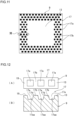
- FIG. 11 is a schematic plan view of an additional copper plate before a semiconductor chip is mounted according to the embodiment 2 of the present invention.
- FIG. 12(A) is a partly enlarged plan view of the additional copper plate in a pat XII of FIG. 11, and
- FIG. 12(B) is a partly enlarged sectional view of the additional copper plate in the pat XII of FIG. 11 .
- FIGs. 13(A) and (B) relate to a modification of the embodiment 2 in which FIG. 13(A) is a partly enlarged plan view of an additional copper plate in the part XII of FIG. 11 , and FIG. 13(B) is a partly enlarged sectional view of the additional copper plate in the part XII of FIG. 11 .
- FIGs. 13(A) is a partly enlarged plan view of an additional copper plate in the part XII of FIG. 11
- FIG. 13(B) is a partly enlarged sectional view of the additional copper plate in the part XII of FIG
- FIGs. 15(A) and (B) relate to another modification of the embodiment 2 in which FIG. 14(A) is a partly enlarged plan view of an additional copper plate in the part XII of FIG. 11 , and FIG. 14(B) is a partly enlarged sectional view of the additional copper plate in the part XII of FIG. 11 .
- FIGs. 15(A) and (B) relate to still another modification of the embodiment 2 in which FIG. 15(A) is a partly enlarged plan view of an additional copper plate in the part XII of FIG. 11 , and FIG. 15(B) is a partly enlarged sectional view of the additional copper plate in the part XII of FIG. 11 .
- engagement recessed portions 17a and engagement projected portions 17b of an engagement uneven portion 17 adjacent to each other and intermittently provided are positionally displaced and arranged.
- the engagement recessed portions 17a and the engagement projected portions 17b are arranged at approximate regular pitches.
- the engagement recessed portions 17a and the engagement projected portions 17b are positionally displaced to be arranged, and outflow of solder is more surely suppressed.
- FIGs. 12-15 An individual shape of the engagement uneven portion 17 of the embodiment 2 is as illustrated in FIGs. 12-15 .
- the engagement recessed portion 17a of the engagement uneven portion 17 of FIGs. 12 is formed into a square shape in the plan view of FIG. 12(A) and into an inverted trapezoidal shape in the sectional view of FIG. 12(B) .
- a bottom portion 17aa of the engagement recessed portion 17a is formed flat and a top of the engagement projected portion 17b is a flat face 17d.
- a recess 17c may be formed on the top of the engagement projected portion 17b similarly to the embodiment 1.
- the engagement recessed portion 17a of the engagement uneven portion 17 of FIGs. 13 is formed into a square shape in the plan view of FIG. 13(A) and into an inverted square pyramid shape in the sectional view of FIG. 13(B) .
- the top of the engagement projected portion 17b is the same as of the case of FIGs. 12 .
- the engagement recessed portion 17a of the engagement uneven portion 17 of FIGs. 14 is formed into a circular shape in the plan view of FIG. 14(A) and into an inverted cone shape in the sectional view of FIG. 14(B) .
- the top of the engagement projected portion 17b is the same as of the case of FIGs. 12 .
- the engagement recessed portion 17a of the engagement uneven portion 17 of FIGs. 15 is formed into a circular shape in the plan view of FIG. 15(A) and into a curved cone shape in the sectional view of FIG. 15(B) .
- the top of the engagement projected portion 17b is the same as of the case of FIGs. 12 .
- a tool T is configured so that a tool uneven portion 15 corresponds to the engagement uneven portion 17 of the additional copper plate 9.
- FIG. 16-FIG. 18 relate to the embodiment 3.
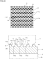
- FIG. 16 is a schematic plan view of an additional copper plate before a semiconductor chip is mounted.
- FIG. 17(A) is a partly enlarged plan view of the additional copper plate in a part XVII of FIG. 16, and
- FIG. 17(B) is a partly sectional view of the additional copper plate in the part XVII of FIG. 16.
- FIGs. 18(A) and (B) relate to a modification of the embodiment 3 in which FIG. 18(A) is a partly enlarged plan view of an additional copper plate in the part XVII of FIG. 16, and
- FIG. 18(B) is a partly enlarged sectional view of the additional copper plate in the part XVII of FIG. 16 .
- an additional copper plate 9 of the embodiment 3 is provided successively with engagement recessed portions 17a and engagement projected portions 17b of an engagement uneven portion 17.
- the present embodiment is provided with three engagement recessed portions 17a with similar square frame shapes so as to surround a whole of a circumference of an attachment plane portion 13, and interspaces between the engagement recessed portions 17a are the engagement projected portions 17b.
- a top of the engagement projected portion 17b of the embodiment 3 is formed flat, a recess may be formed thereon similarly to the embodiment 1.
- FIG. 17 and FIG. 18 An individual shape of the engagement uneven portion 17 of the embodiment 3 is as illustrated in FIG. 17 and FIG. 18 .
- the engagement recessed portion 17a of the engagement uneven portion 17 of FIGs. 17 is formed to have a substantially uniform width in the plan view of FIG. 17(A) and formed into an inverted trapezoidal shape in the sectional view of FIG. 17(B) .
- a bottom portion 17aa of the engagement recessed portion 17a is formed flat and the top of the engagement projected portion 17b is a flat face 17d.
- a recess 17c may be formed on the top of the engagement projected portion 17b similarly to the embodiment 1.
- the engagement recessed portion 17a of the engagement uneven portion 17 of FIGs. 18 is formed to have a substantially uniform width in the plan view of FIG. 18(A) and formed into an inverted triangle shape in the sectional view of FIG. 18(B) .
- the top of the engagement projected portion 17b is the same as of the case of FIGs. 17 .
- FIGs. 19(A) and (B) relate to the embodiment 4 of the present invention in which FIG. 19(A) is a schematic plan view of an additional copper layer before a semiconductor chip is mounted, and FIG. 19(B) is a sectional view of a part XIX of FIG. 19(A) .
- FIG. 20(A) is a schematic plan view of an additional copper layer before an attachment plane portion is formed
- FIG. 20(B) is a sectional view of a part XX of FIG. 20(A) .
- the embodiment 4 has a basic structure in common with the embodiment 1 and corresponding components are represented with the same reference numerals to eliminate repetition in description.
- the present embodiment forms an attachment plane portion 13 on a surface of an additional copper plate 9 by cutting as illustrated in FIG. 19(A)-FIG. 20(B) .
- the present embodiment presses a tool T so as to bring a tool uneven portions into contact with a whole surface of the additional copper plate 9 to apply ultrasonic vibration as illustrated in FIGs. 20(A) and 20(B) , the tool having the tool uneven portion 15 formed on a whole surface or on a whole region to be brought into contact with the surface of the additional copper plate 9.
- the additional copper plate 9 is bonded on the circuit conductor 3a of the circuit pattern 3 with the transmission of the ultrasonic vibration while the surface of the additional copper plate 9 is pressed in the whole area and the engagement uneven portion 17 is formed. This surely bonds the additional copper plate 9 on the circuit conductor 3a while further reducing damage of the insulating layer 7.
- the attachment plane portion 13 is formed by cutting as illustrated in FIGs. 19(A) and (B) .
- the attachment plane portion 13 has a planar shape and a sectional shape similar to the embodiment 1, and the attachment plane portion is arranged lower than a bottom portion of the engagement recessed portion 17a of the engagement uneven portion 17.
- attachment plane portion 13 is cut into a flat face in the present embodiment.
- the attachment plane portion 13 should be, however, a face having unevenness smaller than the engagement uneven portion 17 and accordingly the engagement uneven portion 17 may be slightly remained.
- truncated and lowered engagement projected portions 17b may be remained on the attachment plane portion 13.
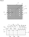
- FIGs. 21(A) and (B) relate to the embodiment 5 of the present invention in which FIG. 21(A) is a schematic plan view of an additional copper layer before a semiconductor chip is mounted, and FIG. 21(B) is a sectional view of a part XXI of FIG. 21(A) .
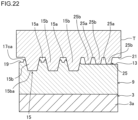
- FIG. 22 is a schematic sectional view of a situation that the additional copper plate is ultrasonic-bonded to a circuit pattern.
- the embodiment 5 has a basic structure in common with the embodiment 1 and corresponding components are represented with the same reference numerals to eliminate repetition in description.
- the present embodiment forms an attachment plane portion 13 by an uneven face having recesses and projections smaller than an engagement uneven portion 17 as illustrated in FIGs. 21(A) and (B) . Others are the same as of the embodiment 1.
- the attachment plane portion 13 of the present embodiment has recesses 23a and projections 23b forming the uneven face.
- the recesses 23a and the projections 23b are configured similarly to the engagement recessed portions 17a and the engagement projected portions 17b, respectively and are smaller than the engagement recessed portions 17a and the engagement projected portions 17b.
- the small in this context means that the recessed portions and the projected portions are small in both a planar shape and a sectional shape, it may mean that the recessed portions and the projected portions are small in any one of the planar shape and the sectional shape.
- the projection 23b of the attachment plane portion 13 corresponds to one in which the engagement projected portion 17b of FIG. 5(A) is made smaller, and is formed by plastically deforming an additional copper plate 9 to bulge from the attachment plane portion 13.
- a top of the projection 23b of the attachment plane portion 13 is, however, lower than the top of the engagement projected portion 17b.
- the projection 23b of the attachment plane portion 13 may be one in which the engagement projected portion 17b of FIG. 4 , FIG. 5(B) , or FIG. 12-FIG. 18(B) is made smaller.
- the attachment plane portion 13 is formed when bonding the additional copper plate 9 on a circuit conductor 3a of a circuit pattern 3 according to ultrasonic vibration using a tool T as illustrated in FIG. 22 .
- the tool T is provided with a reduction uneven portion 25 on a retracted portion 21 to reduce friction against a surface of the additional copper plate 9 in addition to the retracted portion 21 and a tool uneven portion 15 surrounding the retracted portion.
- the reduction uneven portion 25 is provided with reduction recessed portions 25a and reduction projected portions 25b.
- the reduction recessed portions 25a and the reduction projected portions 25b are configured similarly to tool recessed portions 15a and tool projected portions 15b, a sectional shape of the reduction projected portion 25b is a trapezoidal shape, and a sectional shape of the reduction recessed portion 27b is an inverted trapezoidal shape.
- the reduction recessed portions 25a and the reduction projected portions 25b are, however, smaller than the tool recessed portions 15a and the tool projected portions 15b according to the recesses 23a and the projections 23b of the attachment plane portion 13.
- the small in this context means that the reduction recessed portions and the reduction projected portions are small in both a planar shape and a sectional shape, it may mean that the reduction recessed portions and the reduction projected portions are small in any one of the planar shape and the sectional shape similarly to the recesses 23a and the projections 23b.
- the reduction projected portion 25b of the present embodiment corresponds to one in which the tool projected portion 15b of FIG. 7 is made smaller according to the recess 23a of the attachment plane portion 13.
- the reduction projected portion 25b may be, however, one in which the other tool projected portion 15b of FIG. 9 or the like is made smaller according to the recess 23a of the attachment plane portion 13 or may have another shape or the like.
- the reduction uneven portion 25 may be formed into a dimple shape having reduction projected portions 25b with projected curved faces as illustrated in FIG. 23 .
- the reduction uneven portion 25 contacts with the surface of the additional copper plate 9 as well as the tool uneven portion 15 when pressing the tool T against the surface of the additional copper plate 9 layered on the circuit pattern 3 to apply the ultrasonic vibration.
- the additional copper plate 9 is integrally ultrasonic-vibrated relatively to the circuit conductor 3a together with the tool T.
- the peripheral tool uneven portion 15 presses the additional copper plate 9 while forming the engagement uneven portion 17 and the retracted portion 21 presses the additional copper plate 9 through the reduction uneven portion 25.
- the tool T presses and ultrasonic-vibrates the additional copper plate 9 in the whole area, thereby surely bonding the additional copper plate 9 to the circuit conductor 3a.
- the tool T is ultrasonic-vibrated relatively to the additional copper plate 9, and the reduction uneven portion 25 reduces friction between the retracted portion 21 of the tool T and the additional copper plate 9 at this time.
- temperature rise of the additional copper plate 9 is suppressed to further reduce damage of the insulating layer 7.
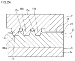
- FIG. 24 is a schematic sectional view of a situation that an additional copper plate is ultrasonic-bonded to a circuit pattern according to the embodiment 6 of the present invention. It should be noted that the embodiment 6 has a basic structure in common with the embodiment 1 and corresponding components are represented with the same reference numerals to eliminate repetition in description.
- the present embodiment presses a retracted portion 21 onto a surface of an additional copper plate 9 through a friction reducing material 27 at the time of ultrasonic vibration for ultrasonic-bonding the additional copper plate 9 on a circuit pattern 3 as illustrated in FIG. 24 .
- Others are the same as of the embodiment 1.
- the retracted portion 21 of the present embodiment is located so as to protrude from a bottom portion of a tool recessed portion 15a of a tool uneven portion 15.
- the friction reducing material 27 may be configured by lubricant such as grease or by a sheet causing shear deformation between the retracted portion 21 and an attachment plane portion 13.
- a ceramics fiber paper or the like may be used, the ceramics fiber paper being ceramics fibers formed into a sheet shape.
- the friction reducing material 27 is interposed between the retracted portion 21 of the tool T and the surface of the additional copper plate 9 when pressing the tool T onto the surface of the additional copper plate 9 layered on the circuit pattern 3 to apply the ultrasonic vibration.
- the additional copper plate 9 is integrally ultrasonic-vibrated relatively to the circuit conductor 3a together with the tool T.
- the peripheral tool uneven portion 15 presses the additional copper plate 9 while forming the engagement uneven portion 17 and the retracted portion 21 presses the additional copper plate 9 through the friction reducing material 27.
- the tool T presses and ultrasonic-vibrates the additional copper plate 9 in the whole area, thereby surely bonding the additional copper plate 9 to the circuit conductor 3a.
- the tool T is ultrasonic-vibrated relatively to the additional copper plate 9, and the friction reducing material 27 reduces friction between the retracted portion 21 of the tool T and the additional copper plate 9 at this time. As a result, temperature rise of the additional copper plate 9 is suppressed to further reduce damage of the insulating layer 7.
Landscapes
- Engineering & Computer Science (AREA)
- Microelectronics & Electronic Packaging (AREA)
- Manufacturing & Machinery (AREA)
- Mechanical Engineering (AREA)
- Cooling Or The Like Of Semiconductors Or Solid State Devices (AREA)
- Pressure Welding/Diffusion-Bonding (AREA)
- Manufacturing Of Printed Wiring (AREA)
- Diaphragms For Electromechanical Transducers (AREA)
- Parts Printed On Printed Circuit Boards (AREA)
Abstract
Description
- The present invention relates to a circuit board and a manufacturing method used for manufacturing the same.
- In recent years, needs for large current of a power device increase more and more and needs for cost reduction of a semiconductor increase at the same time. According to this, it is required for development of a circuit board applicable to large current with low cost.
- There is one disclosed in
Patent document 1 as a conventional circuit board. - A circuit pattern of the circuit board is formed by wet etching conducted to a cupper foil (Cu foil) or an aluminum foil (Al foil).
- For large current and the like, it is important that the Cu foil is made thick to effectively dissipate heat of electronic components such as semiconductor chip mounted on the circuit pattern. If the Cu foil is made thick, processing time for the etching is elongated to also deteriorate dimensional accuracy of the circuit pattern.
- In contrast, in a circuit board disclosed in Patent document 2, a stacked circuit pattern is formed by a cold spray method on a circuit pattern formed by etching conducted to a Cu foil. The circuit board increase heat dissipation according to the stacking that makes the circuit pattern partly thick while suppressing processing time for the etching.
- The cold spray method is, however, a technique to form a coat by colliding particles of thermal spray material in a solid phase with a base material at high speed. Accordingly, large residual stress and thermal stress tend to be generated in a Cu layer of the stacked circuit pattern, and there is concern over a curve of the board. Further, powder is used for raw material to increase the cost.
- In contrast, an ultrasonic bonding technique disclosed in
Patent document 3 may be diverted to stack and bond a metal layer such as additional Cu foil on a circuit pattern such as a Cu foil. The bonding technique is to add ultrasonic vibration in a planar direction of an interface against a circuit pattern while pressing an electrode terminal using an ultrasonic horn, to bond the electrode terminal to the circuit pattern according to the ultrasonic vibration. - If the ultrasonic bonding technique is simply diverted, ultrasonic vibration is added in a planar direction of an interface while pressing the additional metal layer using the ultrasonic horn, to bond the metal layer to the circuit pattern.
- It is, therefore, advantageous that a curve of the board is hard to be caused unlike the cold spray method of Patent document 2 and expensive powder is not used.
- Tool marks (grooves) are, however, left by the pressing of the ultrasonic horn on a surface of the additional metal layer including a mounting surface for an electronic component. Accordingly, mounting an electronic component on the additional metal layer using solder, the solder with low heat conductivity is accumulated and additionally stayed in the tool marks to limit improvement of heat dissipation of the electronic component.
-
- PATENT DOCUMENT 1:
JP 2002-012653 A - PATENT DOCUMENT 2:
JP 2006-319146 A - PATENT DOCUMENT 3:
JP 2016-096172 A - A problem to be solved is that, if an additional metal layer is bonded to a circuit pattern by ultrasonic bonding and an electronic component is mounted on the additional metal layer using solder, it limits improvement of heat dissipation of the electronic component.
- A circuit board according to the present invention is a circuit board comprising a circuit pattern on a base plate and an additional metal layer layered and bonded on the circuit pattern, wherein the additional metal layer comprises an attachment plane portion configured to fix an electronic component using solder, and an engagement uneven portion provided adjacent to the attachment plane portion to be engaged with a tool uneven portion of a tool for vibration transmission to bond the additional metal layer on the circuit pattern with ultrasonic vibration, wherein the attachment plane portion is a face having unevenness smaller than the engagement uneven portion.
- A manufacturing method for the circuit board according to the present invention layers the additional metal layer on the circuit pattern, and presses a tool onto a surface of the additional metal layer to apply ultrasonic vibration, the tool having a retracted portion and a tool uneven portion corresponding to the attachment plane portion and the engagement uneven portion, thereby bonding the additional metal layer on the circuit pattern due to transmission of the ultrasonic vibration while leaving the attachment plane portion on the surface of the additional metal layer in an area according to the retracted portion and forming the engagement uneven portion on the surface of the additional metal layer according to the tool uneven portion.
- The circuit board according to the present invention layers and bonds the additional metal layer onto the circuit pattern, so that heat dissipation of an electronic component is improved according to increase of thickness of the metal layer, the electronic component fixed to the attachment plane portion of the additional metal layer using solder.
- Bonding of the additional metal layer is surely performed by transmitting the ultrasonic vibration in a planar direction using the tool in a state that the tool uneven portion engages with the engagement uneven portion of the metal layer.
- Further, the engagement uneven portion adjacent to the attachment plane portion suppresses outflow of solder when an electronic component is fixed to the attachment plane portion of the additional metal layer.
- The manufacturing method of the circuit board according to the present invention allows outflow of solder fixing an electronic component to be suppressed using the engagement uneven portion having been used when performing bonding by ultrasonic vibration while providing the surface of the additional metal layer with the attachment plane portion.
- The tool used for the manufacturing method of the circuit board according to the present invention easily realizes the manufacturing method of the circuit board.
-
- [
FIG. 1] FIG. 1 is a schematic sectional view of a circuit board before a semiconductor chip is mounted according to anembodiment 1 of the present invention. - [
FIG. 2] FIG. 2 is a schematic sectional view of the circuit board after the semiconductor chip is mounted according to theembodiment 1. - [
FIG. 3] FIG. 3 is a schematic enlarged plan view of an additional copper plate after the semiconductor chip is mounted according to theembodiment 1. - [
FIG. 4] FIG. 4 is a schematic enlarged sectional view taken along a line IV-IV ofFIG. 3 . - [
FIG. 5] FIG. 5(A) is a partly enlarged schematic sectional view of an additional copper plate according to a modification of theembodiment 1, andFIG. 5(B) is a partly enlarged schematic sectional view of an additional copper plate according to an another modification of theembodiment 1. - [
FIG. 6] FIGs. 6(A) and 6(B) are schematic sectional views of a situation that the additional copper plate is ultrasonic-bonded to a circuit pattern. - [
FIG. 7] FIG. 7 is a partly enlarged sectional view of a state that a tool is pressed onto the additional copper plate according to the modification of theembodiment 1. - [
FIG. 8] FIG. 8 is a partly enlarged sectional view illustrating the attachment plane portion and the engagement uneven portion of the additional copper plate according to the modification of theembodiment 1. - [
FIG. 9] FIG. 9 is a partly enlarged sectional view of a state that a tool is pressed onto the additional copper plate according to the other modification of theembodiment 1. - [
FIG. 10] FIG. 10 is a partly enlarged sectional view illustrating the attachment plane portion and the engagement uneven portion of the additional copper plate according to the other modification of theembodiment 1. - [
FIG. 11] FIG. 11 is a schematic plan view of an additional copper plate before a semiconductor chip is mounted according to an embodiment 2 of the present invention. - [
FIG. 12] FIG. 12(A) is a partly enlarged plan view of a pat XII ofFIG. 11, and FIG. 12(B) is a partly enlarged sectional view of the pat XII ofFIG. 11 . - [
FIG. 13] FIGs. 13(A) and (B) relate to a modification of the embodiment 2 in whichFIG. 13(A) is a partly enlarged plan view of the part XII ofFIG. 11 , andFIG. 13(B) is a partly enlarged sectional view of the part XII ofFIG. 11 . - [
FIG. 14] FIGs. 14(A) and (B) relate to a modification of the embodiment 2 in whichFIG. 14(A) is a partly enlarged plan view of the part XII ofFIG. 11 , andFIG. 14(B) is a partly enlarged sectional view of the part XII ofFIG. 11 . - [
FIG. 15] FIGs. 15(A) and (B) relate to a modification of the embodiment 2 in whichFIG. 15(A) is a partly enlarged plan view of the part XII ofFIG. 11 , andFIG. 15(B) is a partly enlarged sectional view of the part XII ofFIG. 11 . - [
FIG. 16] FIG. 16 is a schematic plan view of an additional copper plate before a semiconductor chip is mounted according to anembodiment 3. - [
FIG. 17 ] InFIGs. 17(A) and (B), FIG. 17(A) is a partly enlarged plan view of a part XVII ofFIG. 16, and FIG. 17(B) is a partly sectional view of the part XVII ofFIG. 16 . - [
FIG. 18] FIGs. 18(A) and (B) relate to a modification of theembodiment 3 in whichFIG. 18(A) is a partly enlarged plan view of the part XVII ofFIG. 16, and FIG. 18(B) is a partly enlarged sectional view of the part XVII ofFIG. 16 . - [
FIG. 19] FIGs. 19(A) and (B) relate to an embodiment 4 of the present invention in whichFIG. 19(A) is a schematic plan view of an additional copper layer before a semiconductor chip is mounted, andFIG. 19(B) is a sectional view of a part XIX ofFIG. 19(A) . - [
FIG. 20] FIGs. 20(A) and (B) relate to the embodiment 4 of the present invention in whichFIG. 20(A) is a schematic plan view of an additional copper layer before an attachment plane portion is formed, andFIG. 20(B) is a sectional view of a part XX ofFIG. 20(A) . - [
FIG. 21] FIGs. 21(A) and (B) relate to anembodiment 5 of the present invention in whichFIG. 21(A) is a schematic plan view of an additional copper layer before a semiconductor chip is mounted, andFIG. 21(B) is a sectional view of a part XXI ofFIG. 21(A) . - [
FIG. 22] FIG. 22 is a schematic sectional view of a situation that the additional copper plate is ultrasonic-bonded to a circuit pattern according to theembodiment 5 of the present invention. - [
FIG. 23] FIG. 23 is a schematic sectional view of a situation that an additional copper plate is ultrasonic-bonded to a circuit pattern according to a modification of theembodiment 5. - [
FIG. 24] FIG. 24 is a schematic sectional view of a situation that an additional copper plate is ultrasonic-bonded to a circuit pattern according to an embodiment 6 of the present invention. - The present invention accomplishes an object to further improve heat dissipation of a semiconductor chip mounted on an additional metal layer using solder, the additional metal layer bonded to a circuit pattern diverting an ultrasonic bonding technique as follows.
- A circuit board of the present invention comprises a circuit pattern (3) on a base plate (5) and an additional metal layer (9) layered and bonded on the circuit pattern (3). The additional metal layer (9) comprises an attachment plane portion (13) configured to fix an electronic component (11) using solder, and an engagement uneven portion (17) provided adjacent to the attachment plane portion (13) to be engaged with a tool uneven portion (15) of a tool (T) for vibration transmission to bond the additional metal layer (9) on the circuit pattern (3) with ultrasonic vibration. The attachment plane portion (13) is a face having unevenness smaller than the engagement uneven portion (17).
- Since the attachment plane portion (13) should be the face having unevenness smaller than the engagement uneven portion (17), and the attachment plane portion may be a flat surface or an uneven surface having recesses and projections smaller than the engagement uneven portion.
- The engagement uneven portion (17) may be embodied by having engagement projected portions (17b) projecting from the attachment plane portion (13). The unevenness of the engagement uneven portion (17) is, however, relative, and the engagement uneven portion may be embodied by having the engagement projected portions (17b) having a height flushing with the attachment plane portion (13) or having a lower projection portions (17b) than the attachment plane portion (13). The engagement projected portions (17b) projecting from the attachment plane portion (13) may be embodied by bulging from the attachment plane portion (13) by plastically deforming the additional metal layer (9). The engagement projected portion (17b) may be embodied by having a recess (17c) or a flat face (17d) on a top. Further, the engagement uneven portion (17) may be embodied by having tilted side faces (17e).
- The engagement uneven portion (17) is indentation of the tool uneven portion (15). The engagement uneven portion (17) may be formed by pressing of a special tool separated from the tool (T) for transmitting ultrasonic vibration. The engagement uneven portion (17) may be formed on the additional metal layer (9) by cutting, a laser or the like.
- Although the engagement uneven portion (17) and the tool uneven portion (15) may correspond one to one in a case that the engagement uneven portion is formed by the pressing of the tool uneven portion (15), the tool uneven portion (15) may be embodied by setting to have less unevenness than the engagement uneven portion (17) in a case that the engagement uneven portion (17) is formed by cutting, a laser or the like.
- The engagement uneven portion (17) may be provided on a whole or part of a circumference surrounding the attachment plane portion (13). The engagement uneven portion (17) should be engaged with the tool uneven portion (15) of the tool, transmit the ultrasonic vibration to the additional metal layer (9), and suppress at least part of outflow of solder.
- The engagement uneven portion (17) may be embodied by being provided intermittently or successively with engagement recessed portions (17a) and engagement projected portions (17b). The engagement recessed portions (17a) and the engagement projected portions (17b) intermittently provided may be embodied by any of that engagement recessed portions (17a) and engagement projected portions (17b) adjacent to each other are aligned in a circumferential direction and a circumference-intersection direction, that the engagement recessed portions and engagement projected portions adjacent to each other are regularly positionally displaced, or that the engagement recessed portions and the engagement projected portions adjacent to each other are randomly arranged. The successive engagement uneven portion (17) may be embodied by that the engagement recessed portions (17a) and the engagement projected portions (17b) are successive in the whole of the circumference surrounding the attachment plane portion (13) or that the engagement recessed portions and the engagement projected portions are intermittently successive.
- A manufacturing method for manufacturing the circuit board uses the tool (T) having a retracted portion (21) and the tool uneven portion (15) corresponding to the attachment plane portion (13) and the engagement uneven portion (17). Namely, the additional metal layer (9) is layered on the circuit pattern (3), and the tool (T) is pressed onto a surface of the additional metal layer (9) to apply ultrasonic vibration. This bonds the additional metal layer (9) on the circuit pattern (3) due to transmission of the ultrasonic vibration while leaving the attachment plane portion (13) on the surface of the additional metal layer (9) in an area according to the retracted portion (21) and forming the engagement uneven portion (17) on the surface of the additional metal layer (9) according to the tool uneven portion (15).
- At the time of the ultrasonic vibration, a friction reducing material (27) may be interposed between the retracted portion (21) and the surface of the additional metal layer (9), to press the retracted portion (21) onto the surface of the additional metal layer (9) through the friction reducing material (27). Further, the retracted portion (21) may have a reduction uneven portion (25) to reduce friction against the surface of the additional metal layer (9), and the reduction uneven portion (25) may be pressed onto the surface of the additional metal layer (9).
- In the manufacturing method of the circuit board, pressing load of the tool (T) pressed onto the surface of the additional metal layer (9) may be in a degree to bulge the engagement projected portions (17b) of the engagement uneven portion (17) from the attachment plane portion (13) integrally with the additional metal layer (9).
- Further, the pressing load of the tool may be in a degree to form the recess (17c) or a flat face (17d) on the top of the engagement projected portion (17b).
- The tool (T) used in the manufacturing method of the circuit board is provided with the retracted portion (21) and the tool uneven portion (15) corresponding to the attachment plane portion (13) and the engagement uneven portion (17).
-
FIG. 1 is a schematic sectional view of a circuit board before a semiconductor chip is mounted according to theembodiment 1.FIG. 2 is a schematic sectional view of the circuit board after the semiconductor chip is mounted. - A
circuit board 1 ofFIG. 1 and FIG. 2 is one that a circuit pattern being partially thicken by an additional metal layer as acircuit board 3 adapted to needs for large current. - The
circuit board 1 is a metal-based circuit board being provided with thecircuit pattern 3 on ametal base plate 5 through an insulatinglayer 7. Thecircuit board 1, however, may be a ceramic circuit board in which acircuit pattern 3 is formed on a ceramic base plate or the like. Anadditional copper plate 9 as an additional metal layer is layered on and bonded to thecircuit pattern 3. With this, thecircuit pattern 3 is partially thicken and improved in heat dissipation. - The
circuit pattern 3 is formed of a circuit copper material, a thickness of which is 0.5mm for example. The thickness of thecircuit pattern 3 is set in view of etching process time and may be a thickness selected other than 0.5mm. Thecircuit pattern 3 may be formed of aluminum or the like. - The
circuit pattern 3 is formed by etching and is provided with a plurality ofcircuit conductors 3a. A configuration of the plurality of thecircuit conductors 3a corresponds to required characteristics of thecircuit pattern 3. It should be noted that thecircuit pattern 3 may be one formed in advance by pressing or cutting and adhered on themetal base plate 5 through the insulatinglayer 7. - The
metal base plate 5 is made of, for example, a single metal or an alloy, a thickness of which is set to, for example, 2.0mm. Themetal base plate 5 may or may not have flexibility. As the material of themetal base plate 5, aluminum, iron, copper, aluminum alloy, or stainless steel may be used. Themetal base plate 5 may further include nonmetal such as carbon. For example, themetal base plate 5 may include aluminum composited with carbon. Further, themetal base plate 5 may have a single layer structure or a multi-layer structure. - The
metal base plate 5 has high heat conductivity. For example, it has heat conductivity of 370-400W·m-1·K-1 in copper material, 190-220W·m-1·K-1 in aluminum material, or 60-80W·m-1·K-1 in iron material. - In addition, a metal base plate having a heat sink shape may be used for the
circuit board 1. - The insulating
layer 7 functions to electrically insulate thecircuit pattern 3 from themetal base plate 5 and additionally functions as an adhesive to bond them together. Accordingly, resin is generally used for the insulatinglayer 7, a thickness of which is set to 0.13mm for example. - Further, since the insulating
layer 7 requires high heat resistance against high heat generation of elements mounted on thecircuit pattern 3 and high heat conductivity to transmit the heat to themetal base plate 5, the insulatinglayer 7 preferably additionally includes inorganic fillers. - The insulating
layer 7 may be formed of epoxy resin, cyanate resin or the like. To the epoxy resin, for example, an amin-based curing agent, a phenol-based curing agent, an acid anhydride-based curing agent, or an imidazole-based curing agent is combined. To the cyanate resin, for example, dicyandiamide or phenol resin is combined as a curing agent. Further, the insulatinglayer 7 may be formed of liquid crystal polymer such as fully aromatic polyester being thermoplastic resin or the other thermoplastic resin. - The inorganic fillers included in the insulating
layer 7 have preferably superior electric insulation and high heat conductivity, there are, for example, alumina, silica, aluminum nitride, boron nitride, silicon nitride, magnesium oxide and the like, and one or two or more kinds selected from among them may be used. - A filling rate of the inorganic fillers in the insulating
layer 7 may be appropriately set according to a kind of the inorganic fillers. For example, it is preferably 85vol% or less, more preferably 30-85 vol%, on the basis of a whole volume of the resin included in the insulatinglayer 7. - The insulating
layer 7 may further include a coupling agent, a dispersing agent or the like, for example. - In addition, a semi-cured insulating sheet may be used as the insulating
layer 7. -
FIG. 3 is a schematic enlarged plan view of an additional metal layer after the semiconductor chip is mounted.FIG. 4 is a schematic enlarged sectional view of the additional metal layer after the semiconductor chip is mounted taken along a line IV-IV ofFIG. 3 .FIGs. 5(A) and 5(B) relate to modifications, in whichFIG. 5(A) is a partly enlarged schematic sectional view of a state that a semiconductor chip is mounted on an additional copper plate having a recess at a top of an engagement projected portion, andFIG. 5(B) is a partly enlarged schematic sectional view of a state that a semiconductor chip is mounted on an additional copper plate having a flat face on a top of an engagement projected portion. - As illustrated in
FIGs. 1-4 , theadditional copper plate 9 as the additional metal layer is formed of copper plate material, and is provided with anattachment plane portion 13 and an engagementuneven portion 17. It should be noted that the additional metal layer may employ appropriate material according to thecircuit pattern 3, and may be formed of an additional aluminum plate using aluminum plate material or the like, for example. - The
additional copper plate 9 is bonded to a selectedcircuit conductor 3a of thecircuit pattern 3. Theadditional copper plate 9 is, for example, 10 mm square and 1.0mm thick. It should be noted that theadditional copper plate 9 is to increase the thickness of thecircuit conductor 3a, dimensions of which correspond to of thetarget circuit conductor 3a orsemiconductor chip 11. - The
attachment plane portion 13 is to mount thesemiconductor chip 11 as an electronic component using solder thereon. Theattachment plane portion 13 is a face having unevenness smaller than the engagementuneven portion 17, and is wholly a flat face according to the present embodiment. Theattachment plane portion 13 may be, however, realized by that even recessed portions and the like are partially or wholly existed. - A planer shape of the
attachment plane portion 13 is formed similarly to an outer contour shape of thesemiconductor chip 11 to be mounted in a plan view. Theattachment plane portion 13 is set into a substantial square shape larger than thesemiconductor chip 11 having a square shape in the plan view. - The
attachment plane portion 13 may be, however, different from the outer contour shape of thesemiconductor chip 11 in the plan view. For example, theattachment plane portion 13 may be a circular shape or the like in the plan view. Further, the planar shape of theattachment plane portion 13 may be smaller than of thesemiconductor chip 11 or be equivalent to of thesemiconductor chip 11. - The engagement
uneven portion 17 is provided adjacent to theattachment plane portion 13 to be engaged with a tool uneven portion 15 (explained later withFIG. 7 ) of a tool T (explained later withFIG. 7 ) for vibration transmission to bond theadditional copper plate 9 on thecircuit pattern 3 with ultrasonic vibration in a planar direction. The engagementuneven portion 17 has been used as one to engage the tooluneven portion 15 therewith in a state that theadditional copper plate 9 is bonded on thecircuit pattern 3. Further, the engagementuneven portion 17 is provided to suppress outflow of solder outside theadditional copper plate 9. - It should be noted that adjacency of the engagement
uneven portion 17 to theattachment plane portion 13 may be any of a position contacting an outer edge of theattachment plane portion 13 or an outer position distanced from the outer edge of theattachment plane portion 13. - The engagement
uneven portion 17 is provided with engagement recessedportions 17a and engagement projectedportions 17b. The engagement recessedportions 17a and the engagement projectedportions 17b are provided intermittently on a whole of a circumference surrounding theattachment plane portion 13. - The intermittence of the engagement recessed
portions 17a and the engagement projectedportions 17b on the whole of the circumference of theattachment plane portion 13 means that the engagement recessedportions 17a and the engagement projectedportions 17b are regularly arranged at uniform intervals along each side of the squareattachment plane portion 13. Distances between the engagement recessedportions 17a and the engagement projectedportions 17b may be set randomly. - The engagement recessed
portions 17a and the engagement projectedportions 17b are aligned and formed in two or three lines between each side of an outer edge of the square shape of theadditional copper plate 9 and theattachment plane portion 13. The number of the lines is not particularly limited and may be increased or reduced. The number of the lines on each side of the square shape may be different. - The engagement recessed
portions 17a and the engagement projectedportions 17b may be provided on part of the circumference surrounding theattachment plane portion 13. - As illustrated in
FIG. 3 and FIG. 4 , the engagement recessedportion 17a of the engagementuneven portion 17 is formed into a square shape in the plan view, and into an inverted square pyramid shape in the sectional view. As this result, the engagementuneven portion 17 has tilted side faces 17e. The tilting in this context means tilting relative to a thickness direction of theadditional copper plate 9. - As illustrated in
FIG. 4 , a bottom of the engagement recessedportion 17a of the engagementuneven portion 17 is lower than theattachment plane portion 13. The engagementuneven portion 17 should be one to engage the tool uneven portion 15 (explained later inFIG. 7 ) therewith and suppress outflow of solder, and the shape of the engagement recessedportion 17a is not particularly limited, and may be a recessed portion formed by a curved surface or the like. - The engagement projected
portions 17b of the engagementuneven portion 17 is set so as to protrude from theattachment plane portion 13. The engagementuneven portion 17 including the engagement recessedportions 17a and the engagement projectedportions 17b is indentation of the tooluneven portion 15 to be explained later, and the engagement projectedportions 17b are formed to be bulged from theattachment plane portion 13 by plastically deforming of theadditional copper plate 9. - The engagement projected
portion 17b may be provided with arecess 17c on a top as the modification ofFIG. 5(A) or may be provided with aflat face 17d on a top as the other modification ofFIG. 5(B) . - The
recess 17c ofFIG. 5(A) is formed by a bulged portion 17ca on a periphery of an opening of the engagement recessedportion 17a. The bulged portion 17ca of the engagement recessedportion 17a nearest to theattachment plane portion 13 is adjacent to theattachment plane portion 13 in the plan view. On the outer periphery of theadditional copper plate 9, the bulged portion 17ca is adjacent to aflat plane portion 19 on the outer periphery. In addition, the engagementuneven portion 17 may be formed up to the outer periphery of theadditional copper plate 9, and theflat plane portion 19 on the outer periphery may not be provided. Theflat plane portion 19 is a common surface of theadditional copper plate 9 before the engagementuneven portion 17 is formed and is the same level as theattachment plane portion 13. - As the other modification of
FIG. 5(B) , in a case that the engagement projectedportion 17b has theflat face 17d on its top, the bulged portion 17ca is adjacent to theattachment plane portion 13 and the outer periphery of theflat plane portion 19 similar to theadditional copper plate 9 of the modification ofFIG. 5(A) . - The
semiconductor chip 11 is fixed to theattachment plane portion 13 with solder. Thesemiconductor chip 11 is connected to theother circuit conductors 3a through aluminum wires or the like not illustrated. - As mentioned above, the
circuit board 1 has thecircuit pattern 3 being partially thicken by ultrasonic-bonding theadditional copper plate 9 on thecircuit conductor 3a. - This further improves heat dissipation of the
semiconductor chip 11 mounted on theattachment plane portion 13 of theadditional copper plate 9 with the solder according to the increase of the thickness by means of theadditional copper plate 9. - In the
additional copper plate 9, the centralattachment plane portion 13 is the flat face. Accordingly, on theattachment plane portion 13 for thesemiconductor chip 11, the solder is suppressed from being unnecessarily remained between thesemiconductor chip 11 and theattachment plane portion 13 at the time of the mounting of thesemiconductor chip 11. This suppresses reduction of the heat dissipation of thecircuit board 1. - When the solder to fix the
semiconductor chip 11 to theattachment plane portion 13 flows out from theattachment plane portion 13 toward the circumference at the time of the mounting of thesemiconductor chip 11, the engagementuneven portion 17 suppresses outflow of the solder. Namely, the outflow of the solder outside theadditional copper plate 9 is suppressed. - Further, the
attachment plane portion 13 is surrounded by the engagementuneven portion 17, thereby mounting thesemiconductor chip 11 while theattachment plane portion 13 is easily recognized. - The engagement
uneven portion 17 provided on theadditional copper plate 9 has the bulged portion 17ca protruding from theattachment plane portion 13 as a mountain against theattachment plane portion 13 as a reference face. - This further improves the function of the used engagement
uneven portion 17 to suppress outflow of the solder outside theadditional copper plate 9. -
FIGs. 6(A) and 6(B) are schematic sectional views of a situation of ultrasonic-bonding to the circuit pattern according to theembodiment 1.FIG. 7 is a partly enlarged sectional view of a state that the tool is pressed onto the additional copper plate according to the modification of theembodiment 1.FIG. 8 is a partly enlarged sectional view illustrating the attachment plane portion and the engagement uneven portion of the additional copper plate according to the modification of theembodiment 1.FIG. 9 is a partly enlarged sectional view of a state that the tool is pressed onto the additional copper plate in the other modification of theembodiment 1.FIG. 10 is a partly enlarged sectional view illustrating the attachment plane portion and the engagement uneven portion of the additional copper plate according to the other modification of theembodiment 1. - Although the manufacturing method of the circuit board according to the embodiment of the present invention will be explained representatively for the modification of
FIGs. 7 and 8 , and the other modification ofFIGs. 9 and 10 , the manufacturing method is common even in the example ofFIGs. 3 and 4 . - As illustrated in
FIG. 6 , the manufacturing method uses the tool T. In addition,FIG. 6(A) is an example using the tool T being 12mm square larger than theadditional copper plate 9 being 10mm square.FIG. 6(B) is an example using the tool T being 5.8mm square smaller than theadditional copper plate 9 being 10mm square for example. - The tool T is provided with a retracted
portion 21 and the tooluneven portion 15 corresponding to theattachment plane portion 13 and the engagementuneven portion 17 in the sectional view ofFIG. 7 . - The tool T corresponds to the planar shape and the sectional shape of the
additional copper plate 9 ofFIG. 3 andFIG. 5(A) , the retractedportion 21 of which is formed in a center of a bottom face being a flat surface and the tooluneven portion 15 of which is formed around the retracted portion. - The retracted
portion 21 is a flat face and forms a distance with respect to theattachment plane portion 13 when pressing the tool T onto theadditional copper plate 9. The retractedportion 21 may, however, contact theattachment plane portion 13. The retractedportion 21 should be retracted relatively to the tooluneven portion 15. The retracting means a degree that theattachment plane portion 13 being the face having the unevenness smaller than the engagementuneven portion 17 is left according to the presence of the retractedportion 21 in a state that the tool T is completely pressed onto the surface of theadditional copper plate 9. Namely, the retracting includes the retractedportion 21 contacting theattachment plane portion 13 or forming a distance to the attachment plane portion in a state that the retractedportion 21 presses theadditional copper plate 9 to form theattachment plane portion 13 and completes the pressing in process that the tool T is pressed onto the surface of theadditional copper plate 9. A surface shape of the retractedportion 21 such as a curved face or uneven face other than the flat face is freely selected as long as theattachment plane portion 13 is ensured. - The tool
uneven portion 15 is provided intermittently with tool recessedportions 15a and tool projectedportions 15b on a whole of a circumference surrounding the retractedportion 21, the tool recessed portions and the tool projected portions corresponding to the engagement projectedportions 17b and the engagement recessedportions 17a of the engagementuneven portion 17 to form them. The tool recessedportions 15a and the tool projectedportions 15b are formed into relatively reversed trapezoidal shapes in the sectional view. A tip end 15ba of the tool projectedportion 15b is a flat face according to a bottom portion 17aa of the engagement recessedportion 17. - The manufacturing method of the present embodiment using the tool T layers the
additional copper plate 9 on thecircuit pattern 3 and presses the tool T on the surface of theadditional copper plate 9 to apply ultrasonic vibration. This bonds theadditional copper plate 9 on thecircuit conductor 3a of thecircuit pattern 3 according to transmission of the ultrasonic vibration while leaving theattachment plane portion 13 on the surface of theadditional copper plate 9 in an area corresponding to the retractedportion 21 and forming the engagementuneven portion 17 on the surface of theadditional copper plate 9 according to the tooluneven portion 15. - In particular, first, the
metal base plate 5 is fixedly supported using a jig or the like in advance, and theadditional copper plate 9 to be layered is positioned and arranged on any one of thecircuit conductors 3a of thecircuit pattern 3. - Next, the tool T is pressed onto the surface of the
additional copper plate 9 to apply pressure and transmit the ultrasonic vibration in a planar direction of thecircuit conductor 3a. - With the ultrasonic vibration, a plastic flow is caused in bonding surfaces and the
additional copper plate 9 is bonded and connected on thecircuit conductor 3a. - At this time, the
attachment plane portion 13 is left on the surface of theadditional copper plate 9 according to the retractedportion 21 and the engagementuneven portion 17 is formed on the surface of theadditional copper plate 9 according to the tooluneven portion 15 based on the pressing of the tool T against the surface of theadditional copper plate 9. - Pressing load of the tool T onto the
additional copper plate 9 is in a degree to integrally bulge the engagement projectedportions 17b of the engagementuneven portion 17 from theattachment plane portion 13. At this time, the retractedportion 21 may form a distance relative to theattachment plane portion 13 as illustrated inFIG. 7 or the retractedportion 21 may contact theattachment plane portion 13. - According to the degree of the pressing caused by the pressing load of
FIG. 7 , the bulged portion 17ca is formed on the periphery of the opening of the engagement recessedportion 17a as the mountain against theattachment plane portion 13 as the reference face and therecess 17c is left on the top of the engagement projectedportion 17b as illustrated inFIG. 8 . The engagement recessedportion 17a is formed as a valley against theattachment plane portion 13 as the reference face, the bottom portion 17aa of which is formed flat. - In the other modification of
FIG. 9 , the pressing load of the tool T is greater than of the case ofFIG. 7 . According to the degree of the pressing caused by the pressing load ofFIG. 9 , the bulged portion 17ca contacts a flat face in the tool recessedportion 15 as the bottom face of the tool T and the top of the engagement projectedportion 17b is formed into theflat face 17d. - As mentioned above, the manufacturing method of the
embodiment 1 transmits the ultrasonic vibration to theadditional copper plate 9 in the planar direction while forming the engagementuneven portion 17 using the tool T, to bond theadditional copper plate 9 on any of theconductors 3a of thecircuit pattern 3. - The tool T is, therefore, pressed onto the surface of the
additional copper plate 9 and theattachment plane portion 13 is left on the surface of theadditional copper plate 9 in the area corresponding to the retractedportion 21. The ultrasonic vibration is transmitted to theadditional copper plate 9 using the tool T while the engagementuneven portion 17 is formed on the surface of theadditional copper plate 9 according to the tooluneven portion 15 of the tool T, and theadditional copper plate 9 is bonded on thecircuit conductor 3a. - Since the tool T firmly bites into the surface of the
additional copper plate 9 at the tooluneven portion 15 on the outer periphery of the retractedportion 21, good bonding is attained between theadditional copper plate 9 and thecircuit conductor 3a at the time of the ultrasonic-bonding. - The
circuit board 1 manufactured by the manufacturing method is provided with the used engagementuneven portion 17 used at the time of the transmission of the ultrasonic vibration, to suppress the outflow of the solder. - Accordingly, the
attachment plane portion 13 of theadditional copper plate 9 is formed into the flat surface not to unnecessarily keep a remnant of the solder, the attachment plane portion on which thesemiconductor chip 11 is mounted. The structure to suppress the outflow of the solder outside theadditional copper plate 9 by the used engagementuneven portion 17 is easily attained as well as the flatattachment plane portion 13. - The used engagement
uneven portion 17 left on theadditional copper plate 9 by the indentation according to the tooluneven portion 15 is generated by plastically deforming of the surface of theadditional copper plate 9. With the plastic deformation, the bulged portion 17ca is caused on the periphery of the opening of the engagement recessedportion 17a. The bulged portion 17ca is protruded from theattachment plane portion 13 as the mountain against theattachment plane portion 13 as the reference face. - The
additional copper plate 9 is ultrasonic-bonded to thecircuit conductor 3a and it, therefore, shortens the processing time in comparison with a case that an entirelythick circuit pattern 3 is subjected to etching process. - The
additional copper plate 9 generates heat on an interface with respect to thecircuit conductor 3a based on friction according to the ultrasonic bonding. The heat generation is, however, local and instantaneous, and generates no residual stress or suppresses residual stress in comparison with at least the cold spray method. Accordingly, no curve of the circuit board is generated or a curve of the circuit board is suppressed in comparison with at least the cold spray method. - Since the bulk
additional copper plate 9 is used, the manufacturing is performed at low cost in comparison with the cold spray method using powder. -
FIG. 11 is a schematic plan view of an additional copper plate before a semiconductor chip is mounted according to the embodiment 2 of the present invention.FIG. 12(A) is a partly enlarged plan view of the additional copper plate in a pat XII ofFIG. 11, and FIG. 12(B) is a partly enlarged sectional view of the additional copper plate in the pat XII ofFIG. 11 .FIGs. 13(A) and (B) relate to a modification of the embodiment 2 in whichFIG. 13(A) is a partly enlarged plan view of an additional copper plate in the part XII ofFIG. 11 , andFIG. 13(B) is a partly enlarged sectional view of the additional copper plate in the part XII ofFIG. 11 .FIGs. 14(A) and (B) relate to another modification of the embodiment 2 in whichFIG. 14(A) is a partly enlarged plan view of an additional copper plate in the part XII ofFIG. 11 , andFIG. 14(B) is a partly enlarged sectional view of the additional copper plate in the part XII ofFIG. 11 .FIGs. 15(A) and (B) relate to still another modification of the embodiment 2 in whichFIG. 15(A) is a partly enlarged plan view of an additional copper plate in the part XII ofFIG. 11 , andFIG. 15(B) is a partly enlarged sectional view of the additional copper plate in the part XII ofFIG. 11 . - As illustrated in
FIG. 11 , in anadditional copper plate 9 of the embodiment 2, engagement recessedportions 17a and engagement projectedportions 17b of an engagementuneven portion 17 adjacent to each other and intermittently provided are positionally displaced and arranged. The engagement recessedportions 17a and the engagement projectedportions 17b are arranged at approximate regular pitches. - The engagement recessed
portions 17a and the engagement projectedportions 17b are positionally displaced to be arranged, and outflow of solder is more surely suppressed. - An individual shape of the engagement
uneven portion 17 of the embodiment 2 is as illustrated inFIGs. 12-15 . - The engagement recessed
portion 17a of the engagementuneven portion 17 ofFIGs. 12 is formed into a square shape in the plan view ofFIG. 12(A) and into an inverted trapezoidal shape in the sectional view ofFIG. 12(B) . A bottom portion 17aa of the engagement recessedportion 17a is formed flat and a top of the engagement projectedportion 17b is aflat face 17d. Arecess 17c may be formed on the top of the engagement projectedportion 17b similarly to theembodiment 1. - The engagement recessed
portion 17a of the engagementuneven portion 17 ofFIGs. 13 is formed into a square shape in the plan view ofFIG. 13(A) and into an inverted square pyramid shape in the sectional view ofFIG. 13(B) . The top of the engagement projectedportion 17b is the same as of the case ofFIGs. 12 . - The engagement recessed
portion 17a of the engagementuneven portion 17 ofFIGs. 14 is formed into a circular shape in the plan view ofFIG. 14(A) and into an inverted cone shape in the sectional view ofFIG. 14(B) . The top of the engagement projectedportion 17b is the same as of the case ofFIGs. 12 . - The engagement recessed
portion 17a of the engagementuneven portion 17 ofFIGs. 15 is formed into a circular shape in the plan view ofFIG. 15(A) and into a curved cone shape in the sectional view ofFIG. 15(B) . The top of the engagement projectedportion 17b is the same as of the case ofFIGs. 12 . - A tool T is configured so that a tool
uneven portion 15 corresponds to the engagementuneven portion 17 of theadditional copper plate 9. - Even the embodiment 2 provides the same effect as the
embodiment 1. - In addition, the shapes of the engagement
uneven portions 17 ofFIG. 12-FIG. 15 may be applied to theembodiment 1. -
FIG. 16-FIG. 18 relate to theembodiment 3.FIG. 16 is a schematic plan view of an additional copper plate before a semiconductor chip is mounted.FIG. 17(A) is a partly enlarged plan view of the additional copper plate in a part XVII ofFIG. 16, and FIG. 17(B) is a partly sectional view of the additional copper plate in the part XVII ofFIG. 16. FIGs. 18(A) and (B) relate to a modification of theembodiment 3 in whichFIG. 18(A) is a partly enlarged plan view of an additional copper plate in the part XVII ofFIG. 16, and FIG. 18(B) is a partly enlarged sectional view of the additional copper plate in the part XVII ofFIG. 16 . - As illustrated in
FIG. 16 , anadditional copper plate 9 of theembodiment 3 is provided successively with engagement recessedportions 17a and engagement projectedportions 17b of an engagementuneven portion 17. The present embodiment is provided with three engagement recessedportions 17a with similar square frame shapes so as to surround a whole of a circumference of anattachment plane portion 13, and interspaces between the engagement recessedportions 17a are the engagement projectedportions 17b. Although a top of the engagement projectedportion 17b of theembodiment 3 is formed flat, a recess may be formed thereon similarly to theembodiment 1. - An individual shape of the engagement
uneven portion 17 of theembodiment 3 is as illustrated inFIG. 17 and FIG. 18 . - The engagement recessed
portion 17a of the engagementuneven portion 17 ofFIGs. 17 is formed to have a substantially uniform width in the plan view ofFIG. 17(A) and formed into an inverted trapezoidal shape in the sectional view ofFIG. 17(B) . A bottom portion 17aa of the engagement recessedportion 17a is formed flat and the top of the engagement projectedportion 17b is aflat face 17d. Arecess 17c may be formed on the top of the engagement projectedportion 17b similarly to theembodiment 1. - The engagement recessed
portion 17a of the engagementuneven portion 17 ofFIGs. 18 is formed to have a substantially uniform width in the plan view ofFIG. 18(A) and formed into an inverted triangle shape in the sectional view ofFIG. 18(B) . The top of the engagement projectedportion 17b is the same as of the case ofFIGs. 17 . - Even the
embodiment 3 provides the same effect as theembodiment 1. -
FIGs. 19(A) and (B) relate to the embodiment 4 of the present invention in whichFIG. 19(A) is a schematic plan view of an additional copper layer before a semiconductor chip is mounted, andFIG. 19(B) is a sectional view of a part XIX ofFIG. 19(A) . InFIGs. 20(A) and (B), FIG. 20(A) is a schematic plan view of an additional copper layer before an attachment plane portion is formed, andFIG. 20(B) is a sectional view of a part XX ofFIG. 20(A) . It should be noted that the embodiment 4 has a basic structure in common with theembodiment 1 and corresponding components are represented with the same reference numerals to eliminate repetition in description. - The present embodiment forms an
attachment plane portion 13 on a surface of anadditional copper plate 9 by cutting as illustrated inFIG. 19(A)-FIG. 20(B) . - Namely, the present embodiment presses a tool T so as to bring a tool uneven portions into contact with a whole surface of the
additional copper plate 9 to apply ultrasonic vibration as illustrated inFIGs. 20(A) and 20(B) , the tool having the tooluneven portion 15 formed on a whole surface or on a whole region to be brought into contact with the surface of theadditional copper plate 9. - With this, the
additional copper plate 9 is bonded on thecircuit conductor 3a of thecircuit pattern 3 with the transmission of the ultrasonic vibration while the surface of theadditional copper plate 9 is pressed in the whole area and the engagementuneven portion 17 is formed. This surely bonds theadditional copper plate 9 on thecircuit conductor 3a while further reducing damage of the insulatinglayer 7. - Next, the
attachment plane portion 13 is formed by cutting as illustrated inFIGs. 19(A) and (B) . In the present embodiment, theattachment plane portion 13 has a planar shape and a sectional shape similar to theembodiment 1, and the attachment plane portion is arranged lower than a bottom portion of the engagement recessedportion 17a of the engagementuneven portion 17. - In addition, the
attachment plane portion 13 is cut into a flat face in the present embodiment. Theattachment plane portion 13 should be, however, a face having unevenness smaller than the engagementuneven portion 17 and accordingly the engagementuneven portion 17 may be slightly remained. For example, truncated and lowered engagement projectedportions 17b may be remained on theattachment plane portion 13. - In addition, even the embodiment 4 provides the same effect as the
embodiment 1. -
FIGs. 21(A) and (B) relate to theembodiment 5 of the present invention in whichFIG. 21(A) is a schematic plan view of an additional copper layer before a semiconductor chip is mounted, andFIG. 21(B) is a sectional view of a part XXI ofFIG. 21(A) .FIG. 22 is a schematic sectional view of a situation that the additional copper plate is ultrasonic-bonded to a circuit pattern. It should be noted that theembodiment 5 has a basic structure in common with theembodiment 1 and corresponding components are represented with the same reference numerals to eliminate repetition in description. - The present embodiment forms an
attachment plane portion 13 by an uneven face having recesses and projections smaller than an engagementuneven portion 17 as illustrated inFIGs. 21(A) and (B) . Others are the same as of theembodiment 1. - The
attachment plane portion 13 of the present embodiment hasrecesses 23a andprojections 23b forming the uneven face. Therecesses 23a and theprojections 23b are configured similarly to the engagement recessedportions 17a and the engagement projectedportions 17b, respectively and are smaller than the engagement recessedportions 17a and the engagement projectedportions 17b. Although the small in this context means that the recessed portions and the projected portions are small in both a planar shape and a sectional shape, it may mean that the recessed portions and the projected portions are small in any one of the planar shape and the sectional shape. - In addition, the
projection 23b of theattachment plane portion 13 corresponds to one in which the engagement projectedportion 17b ofFIG. 5(A) is made smaller, and is formed by plastically deforming anadditional copper plate 9 to bulge from theattachment plane portion 13. A top of theprojection 23b of theattachment plane portion 13 is, however, lower than the top of the engagement projectedportion 17b. Further, theprojection 23b of theattachment plane portion 13 may be one in which the engagement projectedportion 17b ofFIG. 4 ,FIG. 5(B) , orFIG. 12-FIG. 18(B) is made smaller. - The
attachment plane portion 13 is formed when bonding theadditional copper plate 9 on acircuit conductor 3a of acircuit pattern 3 according to ultrasonic vibration using a tool T as illustrated inFIG. 22 . Namely, the tool T is provided with a reductionuneven portion 25 on a retractedportion 21 to reduce friction against a surface of theadditional copper plate 9 in addition to the retractedportion 21 and a tooluneven portion 15 surrounding the retracted portion. - The reduction
uneven portion 25 is provided with reduction recessedportions 25a and reduction projectedportions 25b. The reduction recessedportions 25a and the reduction projectedportions 25b are configured similarly to tool recessedportions 15a and tool projectedportions 15b, a sectional shape of the reduction projectedportion 25b is a trapezoidal shape, and a sectional shape of the reduction recessed portion 27b is an inverted trapezoidal shape. - The reduction recessed
portions 25a and the reduction projectedportions 25b are, however, smaller than the tool recessedportions 15a and the tool projectedportions 15b according to therecesses 23a and theprojections 23b of theattachment plane portion 13. Although the small in this context means that the reduction recessed portions and the reduction projected portions are small in both a planar shape and a sectional shape, it may mean that the reduction recessed portions and the reduction projected portions are small in any one of the planar shape and the sectional shape similarly to therecesses 23a and theprojections 23b. - In addition, the reduction projected
portion 25b of the present embodiment corresponds to one in which the tool projectedportion 15b ofFIG. 7 is made smaller according to therecess 23a of theattachment plane portion 13. The reduction projectedportion 25b may be, however, one in which the other tool projectedportion 15b ofFIG. 9 or the like is made smaller according to therecess 23a of theattachment plane portion 13 or may have another shape or the like. For example, the reductionuneven portion 25 may be formed into a dimple shape having reduction projectedportions 25b with projected curved faces as illustrated inFIG. 23 . - The reduction
uneven portion 25 contacts with the surface of theadditional copper plate 9 as well as the tooluneven portion 15 when pressing the tool T against the surface of theadditional copper plate 9 layered on thecircuit pattern 3 to apply the ultrasonic vibration. - In an initial stage of the ultrasonic vibration, the
additional copper plate 9 is integrally ultrasonic-vibrated relatively to thecircuit conductor 3a together with the tool T. At this time, the peripheral tooluneven portion 15 presses theadditional copper plate 9 while forming the engagementuneven portion 17 and the retractedportion 21 presses theadditional copper plate 9 through the reductionuneven portion 25. With this, the tool T presses and ultrasonic-vibrates theadditional copper plate 9 in the whole area, thereby surely bonding theadditional copper plate 9 to thecircuit conductor 3a. - After the
additional copper plate 9 and thecircuit conductor 3a are bonded together, the tool T is ultrasonic-vibrated relatively to theadditional copper plate 9, and the reductionuneven portion 25 reduces friction between the retractedportion 21 of the tool T and theadditional copper plate 9 at this time. As a result, temperature rise of theadditional copper plate 9 is suppressed to further reduce damage of the insulatinglayer 7. - In addition, even the
embodiment 5 provides the same effect as theembodiment 1. -
FIG. 24 is a schematic sectional view of a situation that an additional copper plate is ultrasonic-bonded to a circuit pattern according to the embodiment 6 of the present invention. It should be noted that the embodiment 6 has a basic structure in common with theembodiment 1 and corresponding components are represented with the same reference numerals to eliminate repetition in description. - The present embodiment presses a retracted
portion 21 onto a surface of anadditional copper plate 9 through afriction reducing material 27 at the time of ultrasonic vibration for ultrasonic-bonding theadditional copper plate 9 on acircuit pattern 3 as illustrated inFIG. 24 . Others are the same as of theembodiment 1. - The retracted
portion 21 of the present embodiment is located so as to protrude from a bottom portion of a tool recessedportion 15a of a tooluneven portion 15. Thefriction reducing material 27 may be configured by lubricant such as grease or by a sheet causing shear deformation between the retractedportion 21 and anattachment plane portion 13. As the sheet, a ceramics fiber paper or the like may be used, the ceramics fiber paper being ceramics fibers formed into a sheet shape. - The
friction reducing material 27 is interposed between the retractedportion 21 of the tool T and the surface of theadditional copper plate 9 when pressing the tool T onto the surface of theadditional copper plate 9 layered on thecircuit pattern 3 to apply the ultrasonic vibration. - In an initial stage of the ultrasonic vibration, the
additional copper plate 9 is integrally ultrasonic-vibrated relatively to thecircuit conductor 3a together with the tool T. At this time, the peripheral tooluneven portion 15 presses theadditional copper plate 9 while forming the engagementuneven portion 17 and the retractedportion 21 presses theadditional copper plate 9 through thefriction reducing material 27. With this, the tool T presses and ultrasonic-vibrates theadditional copper plate 9 in the whole area, thereby surely bonding theadditional copper plate 9 to thecircuit conductor 3a. - After the
additional copper plate 9 and thecircuit conductor 3a are bonded together, the tool T is ultrasonic-vibrated relatively to theadditional copper plate 9, and thefriction reducing material 27 reduces friction between the retractedportion 21 of the tool T and theadditional copper plate 9 at this time. As a result, temperature rise of theadditional copper plate 9 is suppressed to further reduce damage of the insulatinglayer 7. - In addition, even the embodiment 6 provides the same effect as the
embodiment 1. -
- 1
- Circuit board
- 3
- Circuit pattern
- 3a
- Circuit conductor
- 5
- Metal base plate (base plate)
- 7
- Insulating layer
- 9
- Additional copper plate (Additional metal layer)
- 11
- Semiconductor chip
- 13
- Attachment plane portion
- 15
- Tool uneven portion
- 15a
- Tool recessed portion
- 15b
- Tool projected portion
- 17
- Engagement uneven portion
- 17a
- Engagement recessed portion
- 17aa
- Bottom portion
- 17b
- Engagement projected portion
- 17c
- Recess
- 17ca
- Bulged portion
- 17d
- Flat face
- 19
- Flat plane portion
- 21
- Retracted portion
- 25
- Reduction uneven portion
- 27
- Friction reducing material
- T
- Tool
Claims (16)
- A circuit board comprising:a circuit pattern on a base plate and an additional metal layer layered and bonded on the circuit pattern, whereinthe additional metal layer comprises:an attachment plane portion configured to fix an electronic component using solder; andan engagement uneven portion provided adjacent to the attachment plane portion to be engaged with a tool uneven portion of a tool for vibration transmission to bond the additional metal layer on the circuit pattern with ultrasonic vibration, whereinthe attachment plane portion is a face having unevenness smaller than the engagement uneven portion.
- The circuit board according to claim 1, wherein
the attachment plane portion is a flat surface. - The circuit board according to claim 1, wherein
the attachment plane portion is an uneven face having unevenness smaller than the engagement uneven portion. - The circuit board according to any one of claims 1-3, wherein
the engagement uneven portion is provided on a whole or part of a circumference surrounding the attachment plane portion. - The circuit board according to any one of claims 1-4, wherein
the engagement uneven portion is provided intermittently or successively with engagement recessed portions and engagement projected portions. - The circuit board according to claim 5, wherein
in the engagement recessed portions and the engagement projected portions intermittently provided, engagement recessed portions and engagement projected portions adjacent to each other are aligned or positionally displaced. - The circuit board according to any one of claims 1-6, wherein
the engagement uneven portion is provided with engagement projected portions projecting from the attachment plane portion. - The circuit board according to claim 7, wherein
the engagement projected portions are bulged from the attachment plane portion by plastically deforming the additional metal layer. - The circuit board according to claim 7 or 8, wherein
the engagement projected portion has a recess or a flat face on a top. - The circuit board according to any one of claims 1-9, wherein
the engagement uneven portion is indentation of the tool uneven portion. - The circuit board according to any one of claims 1-9, wherein
the engagement uneven portion has tilted side faces. - A manufacturing method for the circuit board according to any one of claims 1-11, comprising:layering the additional metal layer on the circuit pattern; andpressing a tool onto a surface of the additional metal layer to apply ultrasonic vibration, the tool having a retracted portion and a tool uneven portion corresponding to the attachment plane portion and the engagement uneven portion, thereby bonding the additional metal layer on the circuit pattern due to transmission of the ultrasonic vibration while leaving the attachment plane portion on the surface of the additional metal layer in an area according to the retracted portion and forming the engagement uneven portion on the surface of the additional metal layer according to the tool uneven portion.
- The manufacturing method of the circuit board according to claim 12, wherein
interposing a friction reducing material between the retracted portion and the surface of the additional metal layer at the time of the ultrasonic vibration, to press the retracted portion onto the surface of the additional metal layer through the friction reducing material. - The manufacturing method of the circuit board according to claim 12, whereinthe retracted portion has a reduction uneven portion to reduce friction against the surface of the additional metal layer, andthe reduction uneven portion is pressed onto the surface of the additional metal layer.
- The manufacturing method of the circuit board according to any one of claims 12-14, wherein
pressing load of the tool pressed onto the surface of the additional metal layer is in a degree to bulge the engagement projected portions of the engagement uneven portion from the attachment plane portion by plastically deforming the additional metal layer. - The manufacturing method according to claim 15, wherein
the pressing load of the tool is in a degree to form the recess or a flat face on the top of the engagement projected portion of the engagement uneven portion.
Applications Claiming Priority (2)
| Application Number | Priority Date | Filing Date | Title |
|---|---|---|---|
| JP2021020504 | 2021-02-12 | ||
| PCT/JP2022/003154 WO2022172767A1 (en) | 2021-02-12 | 2022-01-27 | Circuit board and manufacturing method |
Publications (2)
| Publication Number | Publication Date |
|---|---|
| EP4292743A1 true EP4292743A1 (en) | 2023-12-20 |
| EP4292743A4 EP4292743A4 (en) | 2024-08-07 |
Family
ID=82838757
Family Applications (1)
| Application Number | Title | Priority Date | Filing Date |
|---|---|---|---|
| EP22752596.1A Pending EP4292743A4 (en) | 2021-02-12 | 2022-01-27 | PRINTED CIRCUIT BOARD AND MANUFACTURING METHOD |
Country Status (6)
| Country | Link |
|---|---|
| US (1) | US20240234366A9 (en) |
| EP (1) | EP4292743A4 (en) |
| JP (3) | JP7375229B2 (en) |
| CN (1) | CN116830260A (en) |
| TW (1) | TWI803175B (en) |
| WO (1) | WO2022172767A1 (en) |
Families Citing this family (2)
| Publication number | Priority date | Publication date | Assignee | Title |
|---|---|---|---|---|
| WO2025100065A1 (en) * | 2023-11-10 | 2025-05-15 | 日本発條株式会社 | Circuit board and method for production thereof |
| WO2025100064A1 (en) * | 2023-11-10 | 2025-05-15 | 日本発條株式会社 | Circuit board and manufacturing method therefor |
Family Cites Families (34)
| Publication number | Priority date | Publication date | Assignee | Title |
|---|---|---|---|---|
| JPS52124865A (en) * | 1976-04-13 | 1977-10-20 | Sharp Corp | Semiconductor device |
| JPH05235117A (en) * | 1992-02-24 | 1993-09-10 | Matsushita Electric Works Ltd | Method for manufacturing semiconductor device |
| JPH07307553A (en) * | 1994-05-11 | 1995-11-21 | Nitto Denko Corp | Method for forming metal thin film on metal substrate |
| US6204454B1 (en) * | 1997-12-27 | 2001-03-20 | Tdk Corporation | Wiring board and process for the production thereof |
| JP3928682B2 (en) * | 1999-06-22 | 2007-06-13 | オムロン株式会社 | Wiring board bonded body, wiring board bonding method, data carrier manufacturing method, and electronic component module mounting apparatus |
| JP2002050730A (en) | 2000-08-01 | 2002-02-15 | Densho Engineering:Kk | Lead frame and manufacturing method thereof |
| US7049683B1 (en) * | 2003-07-19 | 2006-05-23 | Ns Electronics Bangkok (1993) Ltd. | Semiconductor package including organo-metallic coating formed on surface of leadframe roughened using chemical etchant to prevent separation between leadframe and molding compound |
| JP4585196B2 (en) | 2003-12-16 | 2010-11-24 | 富士通セミコンダクター株式会社 | Electronic component bonding method and apparatus |
| JP4170968B2 (en) * | 2004-02-02 | 2008-10-22 | 松下電器産業株式会社 | Optical device |
| US20060180635A1 (en) * | 2005-02-17 | 2006-08-17 | Oon-Pin Lim | Bonding tool and method |
| JP2006245171A (en) | 2005-03-02 | 2006-09-14 | Toshiba Corp | Electronic component module |
| JP4857594B2 (en) * | 2005-04-26 | 2012-01-18 | 大日本印刷株式会社 | Circuit member and method of manufacturing circuit member |
| JP4503039B2 (en) * | 2006-04-27 | 2010-07-14 | 三洋電機株式会社 | Circuit equipment |
| JP4372162B2 (en) | 2007-01-26 | 2009-11-25 | 株式会社東芝 | Ultrasonic bonding jig |
| JP2010123680A (en) | 2008-11-18 | 2010-06-03 | Toshiba Corp | Semiconductor device, connection conductor, and method of manufacturing semiconductor device |
| US8426959B2 (en) * | 2009-08-19 | 2013-04-23 | Samsung Electronics Co., Ltd. | Semiconductor package and method of manufacturing the same |
| US9287191B2 (en) * | 2011-10-12 | 2016-03-15 | Taiwan Semiconductor Manufacturing Company, Ltd. | Semiconductor device package and method |
| JP2014007363A (en) * | 2012-06-27 | 2014-01-16 | Renesas Electronics Corp | Method of manufacturing semiconductor device and semiconductor device |
| JP6050140B2 (en) | 2013-02-20 | 2016-12-21 | 昭和電工株式会社 | Insulating substrate |
| JP6150938B2 (en) * | 2014-04-04 | 2017-06-21 | 三菱電機株式会社 | Semiconductor device |
| JP6651924B2 (en) | 2016-03-17 | 2020-02-19 | 三菱マテリアル株式会社 | Method of manufacturing bonded body and method of manufacturing power module substrate |
| JP6561331B2 (en) * | 2016-03-30 | 2019-08-21 | パナソニックIpマネジメント株式会社 | Semiconductor device |
| US11631653B2 (en) * | 2017-02-03 | 2023-04-18 | Mitsubishi Electric Corporation | Ultrasonic bonding apparatus, ultrasonic bonding inspection method and ultrasonically-bonded portion fabrication method |
| JP6844309B2 (en) | 2017-02-27 | 2021-03-17 | 住友電気工業株式会社 | Manufacturing method of semiconductor module |
| JP6827386B2 (en) * | 2017-08-15 | 2021-02-10 | イーグル工業株式会社 | Ultrasonic bonding jig, ultrasonic bonding method and bonding structure |
| TWI746883B (en) * | 2017-09-29 | 2021-11-21 | 韓商Jmj韓國有限公司 | Clip, leadframe and substrate for semiconductor package with finely engraved patterns and the semiconductor package having the same |
| US10607931B2 (en) * | 2018-07-03 | 2020-03-31 | Texas Instruments Incorporated | Semiconductor device with electroplated die attach |
| CN112424919B (en) * | 2018-07-20 | 2023-12-22 | 罗姆股份有限公司 | Semiconductor device and method of manufacturing semiconductor device |
| WO2020090000A1 (en) * | 2018-10-30 | 2020-05-07 | 日立化成株式会社 | Semiconductor device and method for manufacturing same |
| US11239179B2 (en) * | 2018-11-28 | 2022-02-01 | Shiann-Tsong Tsai | Semiconductor package and fabrication method thereof |
| JP6746808B1 (en) * | 2018-12-21 | 2020-08-26 | アオイ電子株式会社 | Semiconductor device and method of manufacturing semiconductor device |
| US10957635B2 (en) * | 2019-03-20 | 2021-03-23 | Texas Instruments Incorporated | Multi-chip package with high thermal conductivity die attach |
| US11715678B2 (en) * | 2020-12-31 | 2023-08-01 | Texas Instruments Incorporated | Roughened conductive components |
| US12424525B2 (en) * | 2022-08-20 | 2025-09-23 | Amkor Technology Singapore Holding Pte. Ltd. | Semiconductor devices and methods of manufacturing semiconductor devices |
-
2022
- 2022-01-27 WO PCT/JP2022/003154 patent/WO2022172767A1/en not_active Ceased
- 2022-01-27 CN CN202280011700.3A patent/CN116830260A/en active Pending
- 2022-01-27 JP JP2022581312A patent/JP7375229B2/en active Active
- 2022-01-27 EP EP22752596.1A patent/EP4292743A4/en active Pending
- 2022-01-27 US US18/546,088 patent/US20240234366A9/en active Pending
- 2022-01-28 TW TW111103866A patent/TWI803175B/en active
-
2023
- 2023-10-25 JP JP2023183259A patent/JP7756693B2/en active Active
-
2025
- 2025-10-07 JP JP2025169345A patent/JP2026010695A/en active Pending
Also Published As
| Publication number | Publication date |
|---|---|
| US20240234366A9 (en) | 2024-07-11 |
| TWI803175B (en) | 2023-05-21 |
| US20240136325A1 (en) | 2024-04-25 |
| CN116830260A (en) | 2023-09-29 |
| JPWO2022172767A1 (en) | 2022-08-18 |
| EP4292743A4 (en) | 2024-08-07 |
| JP7756693B2 (en) | 2025-10-20 |
| WO2022172767A1 (en) | 2022-08-18 |
| JP2024008960A (en) | 2024-01-19 |
| JP7375229B2 (en) | 2023-11-07 |
| TW202232689A (en) | 2022-08-16 |
| JP2026010695A (en) | 2026-01-22 |
Similar Documents
| Publication | Publication Date | Title |
|---|---|---|
| JP4635564B2 (en) | Semiconductor device | |
| JP5134582B2 (en) | Connection structure and power module | |
| WO2009110376A1 (en) | Leadframe substrate, semiconductor module and method for manufacturing leadframe substrate | |
| JP4926033B2 (en) | Circuit board, package using the same, and electronic device | |
| JP6150866B2 (en) | Power semiconductor device | |
| US20240136325A1 (en) | Circuit board and manufacturing method | |
| US12417957B2 (en) | Structure and method related to a power module using a hybrid spacer | |
| JP6048238B2 (en) | Electronic equipment | |
| WO2018020640A1 (en) | Semiconductor device | |
| JP3850335B2 (en) | Ceramic circuit board | |
| JP2006253354A (en) | Circuit device and manufacturing method thereof | |
| US20240021569A1 (en) | Semiconductor module and method for manufacturing semiconductor module | |
| JP2025507816A (en) | METHOD FOR ATTACHING TERMINAL TO METAL SUBSTRATE STRUCTURE FOR SEMICONDUCTOR POWER MODULE AND SEMICONDUCTOR POWER MODULE | |
| KR102510878B1 (en) | Semiconductor having package housing engraved surface pattern | |
| JP2004311691A (en) | Metal plate for circuit and ceramic circuit board | |
| JP2009158673A (en) | Package and electronic device | |
| JP2017188528A (en) | Semiconductor device | |
| JP4635977B2 (en) | Heat dissipation wiring board | |
| US20240186211A1 (en) | Direct-cooling for semiconductor device modules | |
| JP2008098488A (en) | Thermally conductive substrate and manufacturing method thereof | |
| KR20240110322A (en) | Semiconductor package | |
| JP2019012712A (en) | Power semiconductor device and manufacturing method of power semiconductor device | |
| CN121420693A (en) | Ceramic circuit board and its manufacturing method | |
| WO2021220357A1 (en) | Semiconductor device | |
| JP2004095968A (en) | Semiconductor device |
Legal Events
| Date | Code | Title | Description |
|---|---|---|---|
| STAA | Information on the status of an ep patent application or granted ep patent |
Free format text: STATUS: THE INTERNATIONAL PUBLICATION HAS BEEN MADE |
|
| PUAI | Public reference made under article 153(3) epc to a published international application that has entered the european phase |
Free format text: ORIGINAL CODE: 0009012 |
|
| STAA | Information on the status of an ep patent application or granted ep patent |
Free format text: STATUS: REQUEST FOR EXAMINATION WAS MADE |
|
| 17P | Request for examination filed |
Effective date: 20230808 |
|
| AK | Designated contracting states |
Kind code of ref document: A1 Designated state(s): AL AT BE BG CH CY CZ DE DK EE ES FI FR GB GR HR HU IE IS IT LI LT LU LV MC MK MT NL NO PL PT RO RS SE SI SK SM TR |
|
| DAV | Request for validation of the european patent (deleted) | ||
| DAX | Request for extension of the european patent (deleted) | ||
| A4 | Supplementary search report drawn up and despatched |
Effective date: 20240710 |
|
| RIC1 | Information provided on ipc code assigned before grant |
Ipc: B23K 1/20 20060101ALN20240704BHEP Ipc: B23K 101/42 20060101ALN20240704BHEP Ipc: H01L 23/373 20060101ALN20240704BHEP Ipc: H05K 1/18 20060101ALN20240704BHEP Ipc: H05K 3/24 20060101ALI20240704BHEP Ipc: H05K 3/00 20060101ALI20240704BHEP Ipc: H05K 1/02 20060101ALI20240704BHEP Ipc: H01L 23/36 20060101ALI20240704BHEP Ipc: H01L 23/12 20060101ALI20240704BHEP Ipc: H01L 23/13 20060101ALI20240704BHEP Ipc: B23K 20/10 20060101ALI20240704BHEP Ipc: B23K 1/00 20060101AFI20240704BHEP |
|
| STAA | Information on the status of an ep patent application or granted ep patent |
Free format text: STATUS: EXAMINATION IS IN PROGRESS |
|
| 17Q | First examination report despatched |
Effective date: 20250404 |