EP4287533A1 - Entwurfsverfahren für vorwärtsfehlerkorrektur (fec) und zugehörige vorrichtung - Google Patents
Entwurfsverfahren für vorwärtsfehlerkorrektur (fec) und zugehörige vorrichtung Download PDFInfo
- Publication number
- EP4287533A1 EP4287533A1 EP21927255.6A EP21927255A EP4287533A1 EP 4287533 A1 EP4287533 A1 EP 4287533A1 EP 21927255 A EP21927255 A EP 21927255A EP 4287533 A1 EP4287533 A1 EP 4287533A1
- Authority
- EP
- European Patent Office
- Prior art keywords
- fec
- data
- transmission
- working areas
- lane
- Prior art date
- Legal status (The legal status is an assumption and is not a legal conclusion. Google has not performed a legal analysis and makes no representation as to the accuracy of the status listed.)
- Withdrawn
Links
Images


Classifications
-
- H—ELECTRICITY
- H04—ELECTRIC COMMUNICATION TECHNIQUE
- H04L—TRANSMISSION OF DIGITAL INFORMATION, e.g. TELEGRAPHIC COMMUNICATION
- H04L1/00—Arrangements for detecting or preventing errors in the information received
- H04L1/004—Arrangements for detecting or preventing errors in the information received by using forward error control
- H04L1/0041—Arrangements at the transmitter end
-
- H—ELECTRICITY
- H03—ELECTRONIC CIRCUITRY
- H03M—CODING; DECODING; CODE CONVERSION IN GENERAL
- H03M13/00—Coding, decoding or code conversion, for error detection or error correction; Coding theory basic assumptions; Coding bounds; Error probability evaluation methods; Channel models; Simulation or testing of codes
- H03M13/03—Error detection or forward error correction by redundancy in data representation, i.e. code words containing more digits than the source words
- H03M13/05—Error detection or forward error correction by redundancy in data representation, i.e. code words containing more digits than the source words using block codes, i.e. a predetermined number of check bits joined to a predetermined number of information bits
-
- H—ELECTRICITY
- H03—ELECTRONIC CIRCUITRY
- H03M—CODING; DECODING; CODE CONVERSION IN GENERAL
- H03M13/00—Coding, decoding or code conversion, for error detection or error correction; Coding theory basic assumptions; Coding bounds; Error probability evaluation methods; Channel models; Simulation or testing of codes
- H03M13/27—Coding, decoding or code conversion, for error detection or error correction; Coding theory basic assumptions; Coding bounds; Error probability evaluation methods; Channel models; Simulation or testing of codes using interleaving techniques
-
- H—ELECTRICITY
- H04—ELECTRIC COMMUNICATION TECHNIQUE
- H04L—TRANSMISSION OF DIGITAL INFORMATION, e.g. TELEGRAPHIC COMMUNICATION
- H04L1/00—Arrangements for detecting or preventing errors in the information received
- H04L1/004—Arrangements for detecting or preventing errors in the information received by using forward error control
- H04L1/0045—Arrangements at the receiver end
-
- H—ELECTRICITY
- H04—ELECTRIC COMMUNICATION TECHNIQUE
- H04L—TRANSMISSION OF DIGITAL INFORMATION, e.g. TELEGRAPHIC COMMUNICATION
- H04L1/00—Arrangements for detecting or preventing errors in the information received
- H04L1/004—Arrangements for detecting or preventing errors in the information received by using forward error control
- H04L1/0056—Systems characterized by the type of code used
- H04L1/0057—Block codes
-
- H—ELECTRICITY
- H04—ELECTRIC COMMUNICATION TECHNIQUE
- H04L—TRANSMISSION OF DIGITAL INFORMATION, e.g. TELEGRAPHIC COMMUNICATION
- H04L1/00—Arrangements for detecting or preventing errors in the information received
- H04L1/004—Arrangements for detecting or preventing errors in the information received by using forward error control
- H04L1/0056—Systems characterized by the type of code used
- H04L1/0071—Use of interleaving
-
- G—PHYSICS
- G06—COMPUTING OR CALCULATING; COUNTING
- G06F—ELECTRIC DIGITAL DATA PROCESSING
- G06F11/00—Error detection; Error correction; Monitoring
- G06F11/07—Responding to the occurrence of a fault, e.g. fault tolerance
- G06F11/08—Error detection or correction by redundancy in data representation, e.g. by using checking codes
- G06F11/10—Adding special bits or symbols to the coded information, e.g. parity check, casting out 9's or 11's
Definitions
- This application relates to the field of communication technologies, and in particular, to a forward error correction code FEC design method and a related device.
- Forward error correction forward error correction
- channel coding channel coding
- FEC forward error correction
- channel coding channel coding
- Error recovery is performed by sending additional information along with data, to reduce a bit error rate.
- data on each lane (lane) is interleaved to a plurality of FEC working areas, and burst errors are distributed to a plurality of FEC blocks, so that a burst error correction capability on each lane can be further improved.
- consecutive bit errors occur on a transmission lane in a data transmission process.
- Reed-Solomon (Reed-Solomon, RS) code is FEC code suitable for correcting such burst errors, and is widely used in various commercial scenarios, such as high-density digital video disc (digital video disc, DVD), Blu-ray disc, digital subscriber line (digital subscriber line, DSL), digital video broadcast (digital video broadcast, DVB), and the like.
- An interface service is applied to various scenarios.
- An interface includes a plurality of transmission lanes, and different quantities of transmission lanes need to be used in different scenarios.
- data is interleaved to a fixed quantity of FEC working areas.
- a quantity of used transmission lanes is different, a data interleaving status is also different, increasing an interface circuit scale, design complexity, and production costs.
- This application provides a forward error correction code FEC design method and a related device.
- FEC working areas whose quantity is the same as that of transmission lanes are used, and data on a transmission lane is evenly allocated to each FEC working area, so that a data arrangement structure on each transmission lane can be unified.
- An interface circuit scale and design complexity are reduced, and production costs are effectively reduced.
- a forward error correction code FEC design method includes: determining a quantity of transmission lanes for transmitting data, and determining a plurality of FEC working areas based on the quantity of transmission lanes, where a quantity of the plurality of FEC working areas is the same as the quantity of transmission lanes, the transmission lane is for transmitting the data, and the FEC working area is for performing check and error correction on the data; evenly allocating the data on the transmission lane to each of the plurality of FEC working areas; and processing, by using the plurality of FEC working areas, the data received by each of the plurality of FEC working areas.
- the data on the transmission lane is processed by using the FEC working area that matches the transmission lane, and the data on the transmission lane is evenly allocated to each FEC working area. It can be ensured that each FEC working area receives an equal amount of data per unit time. Because processing performance and a delay of each FEC working area are the same, structures of the FEC block and link transport blocks on each transmission lane after processing by using the FEC working area are the same. A periodicity of a link transport block boundary is also the same, that is, a data arrangement structure on each transmission lane is the same. In this way, an interface circuit scale and design complexity can be reduced, and production costs can be reduced.
- the data on each transmission lane is divided to obtain a plurality of data blocks, where each data block includes X characters, and X is a positive integer greater than 1; and the X characters included in each data block are evenly allocated to the plurality of FEC working areas.
- the data on the transmission lane needs to be divided, to obtain the plurality of data blocks; and when the data on the transmission lane is evenly allocated to the FEC working area, instead of simply performing correspondence between one transmission lane and one FEC working area and allocating all data on the transmission lane to the FEC working area for processing, the X characters included in one data block on each transmission lane are allocated to the plurality of FEC working areas one by one. In this way, data processed by the FEC workspace each time comes from a plurality of transmission lanes, thereby improving an error correction capability.
- each of the plurality of FEC working areas performs calculation each time the X characters are received, to obtain Y FEC check bits corresponding to the X characters; or if the plurality of FEC working areas are in a decoding state, each of the plurality of FEC working areas performs check and error correction on the X characters by using Y FEC check bits corresponding to every received X characters.
- the FEC working area may complete data processing based on a state that the FEC working area is in.
- the FEC working area performs calculation on the X characters obtained through mapping by each transmission lane to obtain the Y FEC check bits. It is easy to understand that data processed by the FEC working area comes from different transmission lanes. Compared with data that is processed by the FEC working area and that comes from the same transmission lane, consecutive bit errors can be converted into sporadic bit errors, which improves the error correction capability.
- the FEC working area uses the Y FEC check bits to check and correct the X characters mapped from each transmission lane.
- a data sequence is inserted between transport blocks transmitted on each of the transmission lanes, where the transport block includes Z data blocks, the data sequence is for delimiting the data transmitted on the transmission lane, and Z is a positive integer greater than 1.
- more layers of structural division may be performed on the data transmitted on each transmission lane.
- the data sequence may be inserted between the transmitted transport blocks.
- the data sequence is not encoded, and is for delimiting the data transmitted on the transmission lane, aligning data between lanes, initializing a scrambling seed, and the like.
- a scramble reset sequence SR is included between the transport blocks transmitted on each of the transmission lanes, the transport block includes Z FEC blocks, and the FEC block includes the X characters and the Y FEC check bits, where X, Y, and Z are positive integers greater than 1.
- the X characters included in the data block are equal to an amount of data processed each time in any one of the plurality of FEC working areas, where the amount of data processed by the FEC working area each time is the amount of data received by the FEC working area in a unit time.
- the data received by the plurality of working areas and the FEC check bit obtained through calculation are inversely mapped to the transmission lane, and each of the transmission lanes includes a plurality of FEC blocks, where each of the plurality of FEC blocks includes the X characters and the Y FEC check bits.
- the FEC blocks on each transmission lane is divided to obtain a plurality of transport blocks, and an SR is inserted between two adjacent transport blocks, where each transport block includes Z FEC blocks, and Z is a positive integer greater than 1.
- each of the plurality of FEC working areas has same processing performance and a same processing delay, and receives a same amount of to-be-processed data in a unit time.
- a data processing apparatus including: a determining unit, configured to determine a quantity of transmission lanes for transmitting data, and determine a plurality of FEC working areas based on the quantity of transmission lanes, where a quantity of the plurality of FEC working areas is the same as the quantity of transmission lanes, the transmission lane is for transmitting the data, and the FEC working area is for performing check and error correction on the data; an allocation unit, configured to evenly allocate the data on the transmission lane to each of the plurality of FEC working areas; and a processing unit, configured to process, by using the plurality of FEC working areas, the data received by each of the plurality of FEC working areas.
- the allocation unit is specifically configured to: divide the data on each transmission lane to obtain a plurality of data blocks, where each data block includes X characters, and X is a positive integer greater than 1; and evenly allocate the X characters included in each data block to the plurality of FEC working areas.
- the processing unit is specifically configured to: if the plurality of FEC working areas are in an encoding state, perform, by using each of the plurality of FEC working areas, calculation each time the X characters are received, to obtain Y FEC check bits corresponding to the X characters; or if the plurality of FEC working areas are in a decoding state, perform, by using each of the plurality of FEC working areas, check and error correction on the X characters by using Y FEC check bits corresponding to every received X characters.
- the processing unit is further configured to insert a data sequence between transport blocks transmitted on each of the transmission lanes, where the transport block includes Z data blocks, the data sequence is for delimiting the data transmitted on the transmission lane, and Z is a positive integer greater than 1.
- a scramble reset sequence SR is included between the transport blocks transmitted on each of the transmission lanes, the transport block includes Z FEC blocks, and the FEC block includes the X characters and the Y FEC check bits, where X, Y, and Z are positive integers greater than 1.
- the X characters included in the data block are equal to an amount of data processed each time in any one of the plurality of FEC working areas, where the amount of data processed by the FEC working area each time is the amount of data received by the FEC working area in a unit time.
- the allocation unit is further configured to inversely map the data received by the plurality of working areas and the FEC check bits obtained through calculation to the transmission lane, where each of the transmission lanes includes a plurality of FEC blocks, and each of the plurality of FEC blocks includes the X characters and the Y FEC check bits.
- the processing unit is further configured to divide the FEC blocks on each transmission lane to obtain a plurality of transport blocks, and insert an SR between two adjacent transport blocks, where each transport block includes Z FEC blocks, and Z is a positive integer greater than 1.
- each of the plurality of FEC working areas has same processing performance and a same processing delay, and receives a same amount of to-be-processed data in a unit time.
- this application provides a data processing apparatus, where the data processing apparatus includes a processor and a transmission interface, and the processor is configured to invoke computer instructions stored in a memory, to perform the method provided in the first aspect or with reference to any implementation of the first aspect.
- this application provides a computer storage medium, where the computer storage medium stores a computer program, and when the computer program is executed by a computer or a processor, a procedure of the method provided in the first aspect or with reference to any implementation of the first aspect can be implemented.
- this application provides a computer program product.
- the computer program product includes instructions. When the instructions are executed by a computer or a processor, the computer or the processor can perform the procedure of the method provided in the first aspect or with reference to any implementation of the first aspect.
- a transmission lane is specifically a lane for transmitting data, and a specific form of the transmission lane may be a wired transmission lane, or may be a wireless transmission lane.
- a transmission interface for example, a high definition multimedia interface (high definition multimedia interface, HDMI), is configured to transmit data by using a plurality of transmission lanes. Different quantities of transmission lanes may be used for data transmission based on different application scenarios. For example, to transmit standard-definition video data, two transmission lanes may be selected, and to transmit high-definition video data, four transmission lanes may be selected.
- an FEC working area is specifically a hardware circuit, and is for performing calculation and check and error correction on data.
- An amount of data processed by each FEC working area is referred to as an FEC block. That is, an amount of data processed by an FEC working area each time is the same as an amount of data included in an FEC block.
- data interleaving is specifically referred to mapping data on a transmission lane to an FEC working area, that is, allocating data on each transmission lane to a plurality of FEC working areas.
- a data arrangement structure is structural division of data transmitted on a transmission lane.
- the transmission lane is configured to transmit data
- to-be-transmitted data includes characters, where one data block includes X characters, and one FEC block includes X characters and Y check bits.
- the Y check bits correspond to the X characters.
- One transport block (which may also be referred to as a link transport block) includes Z FEC blocks, and one SR is inserted between every two adjacent transport blocks.
- the SR may also be some character sequences, but the SR is not encoded and is for delimiting a transport block, initialize a scrambling seed, and the like.
- FIG. 2A Data on the three transmission lanes is interleaved into four different FEC working areas by using four clock cycles. Each FEC working area performs calculation on data obtained by interleaving to obtain a check bit, and then each FEC working area remaps the check bit and the FEC block obtained by the calculation to the previous three transmission lanes.
- FIG. 2B A data arrangement structure on each lane is shown in FIG. 2B .
- a data block Data between a scramble reset (scramble reset, SR) special character and another start super block (start super block, SSB) is referred to as a data block, and the data block includes not only valid data, but also includes a check bit (that is, an RS check bit in the figure) obtained by the FEC working area through calculation.
- the check bit included in the data block can be used to perform check and error correction on the data in the transport block.
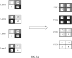
- FIG. 3A Data on the four transmission lanes is interleaved into four different FEC working areas by using two clock cycles.
- Each FEC working area performs calculation on data obtained by interleaving to obtain a check bit, and then each FEC working area remaps the check bit and the FEC block obtained by the calculation to the previous four transmission lanes.
- a data arrangement structure on each lane is shown in FIG. 3B . Similar to FIG. 2B , data between an SR and an SSB is also referred to as a transport block, and the transport block also includes a check bit for performing check and error correction on the data in the transport block.
- this application provides a forward error correction code FEC design method and a related device.
- data on a transmission lane is interleaved by using FEC working areas whose quantity is the same as that of selected transmission lanes.
- Data on the transmission lane is evenly allocated to each FEC working area, and calculation, and check and error correction is performed on data obtained by interleaving by using each FEC working area, so that a same amount of data processed by each FEC working area in a unit time can be ensured, the location of a check bit on each transmission lane is the same, and the boundary of the transport block is the same. Therefore, the interface circuit scale and the design complexity are reduced, and the production costs are effectively reduced.
- FIG. 4 is a schematic diagram of a system architecture according to an embodiment of this application.
- the system includes a data transmitter 410 and a data receiver 420.
- the data transmitter may be specifically a set top box, a monitor, or the like.
- a transmission interface on the data transmitter 410 may flexibly select a quantity of transmission lanes based on a service requirement, and perform FEC encoding on to-be-sent data.
- the data receiver 420 may be specifically a television, a display, or the like. The data receiver 420 receives data from a transmission lane, and performs FEC decoding and error check and correction on the received data.
- the data transmitter 410 transmits the to-be-sent data to a transmission interface 4110, where the transmission interface 4110 includes a plurality of transmission lanes, for example, a transmission lane 0, a transmission lane 1, and a transmission lane 2.
- Transport block structure coding is first performed on data on each transmission lane.
- the data on each transmission lane is processed into periodic transport blocks, and then FEC coding is performed, that is, data on a plurality of transmission lanes is cross-mapped to a plurality of FEC working areas. It should be noted that, a quantity of FEC working areas is the same as a quantity of transmission lanes.
- the data on each transmission lane is evenly allocated to the plurality of FEC working areas, and an amount of data received in each FEC working area in a unit time is the same. Calculation is performed by using the FEC working area on the data to obtain a plurality of check bits, and then the data in the FEC working area is remapped to each transmission lane. It should be understood that a plurality of check bits obtained through calculation in each FEC working area are also cross-mapped to each transmission lane.
- a scrambling operation is performed on the data on each transmission lane to increase the non-coherent capability of the transmission channel to transmit data, and finally through a transmitter, such as a transmitter 4111, a transmitter 4112, and a transmitter 4113, the data on each transmission lane is sent to the data receiver 420 by using the transmission channel.
- the data receiver 420 receives the data sent by the data transmitter 410 by using a plurality of receivers in the transmission interface 4210, for example, a receiver 4211, a receiver 4212, and a receiver 4213, and then performs a descrambling operation on the data on each transmission lane.
- FEC decoding is performed, that is, data on a plurality of transmission lanes is cross-mapped to a plurality of FEC working areas, each FEC working area uses a plurality of check bits to perform check and error correction on the data, and then data obtained after the check bits are removed is cross-mapped to each transmission lane again.
- transport block structure decoding is performed on the data on each transmission lane, and transport blocks on each transmission lane are reprocessed into data streams. In this way, an entire data receiving procedure is completed.
- FIG. 5 is a schematic flowchart of an FEC design method according to an embodiment of this application.
- a data transmitter and a data receiver described in FIG. 5 may respectively correspond to the data transmitter 410 and the data receiver 420 shown in FIG. 4 .
- the method includes but is not limited to the following steps:
- S501 Determine a quantity of transmission lanes for transmitting data, and determine a plurality of FEC working areas based on the quantity of transmission lanes.
- a transmission interface of the data transmitter may flexibly select a quantity of transmission lanes based on a service requirement.
- SD, HD, and 4K video data may be transmitted by using an HDMI.
- the data transmitter selects different quantities of transmission lanes to meet the service requirement. Therefore, before the data is sent, the quantity of transmission lanes for transmitting data needs to be determined first.
- a quantity of FEC working areas matching the transmission lanes needs to be determined.
- a plurality of FEC working areas are manufactured in advance to ensure sufficient redundancy, to meet requirements of different scenarios.
- 10 FEC working area circuits may be manufactured in advance in a design and manufacturing process.
- the transmission interface may support a maximum quantity of 10 transmission lanes. In this way, it can be ensured that the transmission interface meets requirements of various scenarios.
- a quantity of redundant FEC working area circuits may also be set to another value. This is not limited in this application.
- the data transmitted on each transmission lane may be referred to as a data stream.
- the data stream may be divided in a unit of X characters, to obtain a plurality of data blocks.
- a value of X may be flexibly set based on a requirement. This is not limited in this application.
- the data stream on the transmission lane is generally divided based on an amount of data processed by each FEC working area at a time, that is, a value of X is equal to an amount of data processed by each FEC working area at a time.
- the amount of data processed by the FEC working area at a time is the amount of data received by the FEC working area in a unit time.
- FIG. 6 represents a process of data stream division on a transmission lane to obtain a data block.
- Each small block in the figure represents a data unit
- M/N represents an N th data unit in a data block on a lane M.
- 0/0 represents a 0 th data unit in a data block on a lane
- 0/2 represents a second data unit in a data block on a lane 0.
- each FEC working area in a unit time there are three transmission lanes and three FEC working areas.
- One data block on each transmission lane includes 100 characters.
- 300 characters included in three data blocks need to be allocated to three FEC working areas at the same time, so that 100 characters are allocated to each FEC working area.
- a transmission lane is not in a one-to-one correspondence with an FEC working area, and all characters included in a data block on a transmission lane are allocated to an FEC working area.
- each FEC working area processes some data of the data block. For example, in FIG. 6 , each small block has a different color, indicating that the data unit will be allocated to a different FEC working area.
- S503 The plurality of FEC working areas process data received by the plurality of FEC working areas.
- each FEC working area After receiving the data allocated by each transmission lane, each FEC working area starts to process the data.
- the amount of data processed each time is X characters.
- the FEC working area performs calculation on the received X characters to obtain Y FEC check bits, and the Y FEC check bits are separately mapped to each transmission lane.
- the Y check bits may be separately mapped to a plurality of transmission lanes one by one, and then cyclic mapping is performed for a plurality of times until mapping of the Y check bits is completed.
- a specific process is similar to that of allocating characters on a transmission lane to an FEC working area, and reference may be made to the method described above. Details are not described herein again.
- a value of Y is related to a selected check algorithm. If different check algorithms are used, values of Y obtained through calculation may be different.
- a specific selected check algorithm is not limited in this application.
- the FEC working area receives data allocated by each transmission lane. For example, a 0 th data unit in a data block on a lane 0 (that is, 0/0), a first data unit in a data block on a lane 2 (that is, 2/1), and a second data unit in a data block on a lane 1 (that is, 1/2). Then, calculation is performed on the data to obtain Y FEC check bits, where M/PS N represents an FEC check bit, and the check bit is mapped to an N th FEC check bit on a lane M. The Y FEC check bits obtained through performing calculation by the FEC working area are mapped to different transmission lanes.
- a data stream transmitted on each transmission lane may be further divided in structure.
- a data structure formed by X characters included in each data block and Y FEC check bits obtained by mapping from each FEC working area is referred to as an FEC block.
- a specific structure of an FEC block is shown in FIG. 8 .
- 0/0 indicates a 0 th data unit in an FEC block on a lane
- 0/PS 0 indicates a 0 th check bit in an FEC block on a lane 0.
- the FEC working area is an FEC working area of a data receive end
- the data received by the FEC working area includes X characters and Y FEC check bits that are allocated from each transmission lane (that is, the total amount of data received by the FEC working area is the same as the amount of data received by an FEC block.).
- the FEC working area uses the Y FEC check bits to perform check and error correction on the X characters.
- a specific check and error correction process is similar to that of an existing check and error correction algorithm, and details are not described herein again.
- a data sequence that is, a scramble reset sequence (scramble reset sequence, SR)
- SR scramble reset sequence
- one link transport block includes Z FEC blocks
- a value of Z may be set based on a requirement.
- the SR inserted between two LT blocks is not encoded, that is, data in the SR is not allocated to the FEC working area for processing.
- a data structure transmitted on a transmission lane is shown in FIG. 9 .
- An SR is inserted between a link transport block 1 and a link transport block 2, and both include Z FEC blocks.
- a transmission interface includes three transmission lanes, and uses three FEC working areas is used for description.
- data arrangement structures on the transmission lane 0, the transmission lane 1, and the transmission lane 2 are the same, and different link transport blocks are separated by using an SR as a link transport block boundary.
- Each link transport block includes Z FEC blocks.
- Each FEC block includes X characters and Y FEC check bits. Each time an FEC working area 0, an FEC working area 1, and an FEC working area 2 receive X characters mapped from a transmission lane 0, a transmission lane 1, and a transmission lane 2, the Y FEC check bits are obtained through calculation.
- 0 to X-1 indicate data characters allocated by the transmission lane.
- PS0 to PSY-1 indicates the Y check bits obtained through calculation based on the 0 to X-1 characters.
- the arrow from the FEC block on the transmission lane to the FEC working area indicates that data of different FEC blocks is mapped to different FEC working areas. For example, the 0 th data unit of the FEC block 0 on a transmission lane 0 is mapped to the FEC working area 2, the first data unit of the FEC block 0 on the transmission lane 1 is mapped to the FEC working area 0, and the second data unit of the FEC block 0 on the transmission lane 2 is mapped to the FEC working area 1.
- the arrow from the FEC working area to the FEC block on the transmission lane indicates that FEC parity bits obtained through calculation by different FEC working areas are mapped to different FEC blocks. For example, a second check bit on the FEC working area 0 is mapped to the second FEC check bit of the FEC block 0 on the transmission lane 0, a first check bit on the FEC working area 1 is mapped to the first FEC check bit of the FEC block 0 on the transmission lane 0, and a 0 th check bit on the FEC working area 2 is mapped to the 0 th FEC check bit of the FEC block 0 on the transmission lane 0.
- a transmission interface that includes two transmission lanes and that can flexibly select a quantity of lanes to transmit data based on a requirement is used as an example to describe a data processing process in a mode in which different quantities of lanes are used.
- FIG. 11A in a one-lane mode, X to-be-encoded characters included in an FEC block on a lane 0 are sequentially sent to an FEC working area 0 for processing, and Y FEC check bits are obtained through calculation by the FEC working area 0. The Y FEC check bits are inserted after the FEC block immediately following the lane 0, and a data structure of the final transmission is shown in FIG. 11B .
- a two-lane transmission mode data of the FEC blocks of the two lanes is interleaved to the FEC working area 0 and the FEC working area 1. As shown in FIG.
- X to-be-encoded characters included in the FEC block on the lane 0 are evenly allocated to the FEC working area 0 and the FEC working area 1 for processing. For example, a 0 th character is sent to the FEC working area 0, and the first character is sent to the FEC working area 1.
- X to-be-encoded characters included in the FEC block on the lane 1 are also evenly allocated to the FEC working area 0 and the FEC working area 1 for processing. For example, the 0 th character is sent to the FEC working area 1, and the first character is sent to the FEC working area 0.
- FIG. 12B a data structure of the transmission is shown in FIG. 12B .
- Data arrangement structures on the two lanes are the same, SR locations are also the same, and an amount of data included in each link transport block on the lane 0 is the same as an amount of data included in each link transport block on the lane 1.
- an amount of data and a boundary of an FEC block of each lane, an amount of data and a boundary of an LT block, and a periodicity of each lane are the same, that is, a data arrangement structure of each lane is the same, so that data processing can be easily performed by using a unified circuit, an interface circuit scale and design complexity can be reduced, and production costs are effectively reduced.
- FIG. 13 is a schematic structural diagram of a data processing apparatus according to an embodiment of this application.
- a data processing apparatus 100 includes a determining unit 110, an allocation unit 120, and a processing unit 130. Specifically,
- the allocation unit 120 is specifically configured to: divide the data on each transmission lane to obtain a plurality of data blocks, where each data block includes X characters, and X is a positive integer greater than 1; and evenly allocate the X characters included in each data block to the plurality of FEC working areas.
- the processing unit 130 is specifically configured to: if the plurality of FEC working areas are in an encoding state, perform, by using each of the plurality of FEC working areas, calculation each time the X characters are received, to obtain Y FEC check bits corresponding to the X characters; or if the plurality of FEC working areas are in a decoding state, perform, by using each of the plurality of FEC working areas, check and error correction on the X characters by using Y FEC check bits corresponding to every received X characters.
- the processing unit 130 is further configured to insert a data sequence between transport blocks transmitted on each of the transmission lanes, where the transport block includes Z data blocks, the data sequence is for delimiting the data transmitted on the transmission lane, and Z is a positive integer greater than 1.
- the determining unit 110, the allocation unit 120, and the processing unit 130 in embodiments of this application may be implemented by a processor or a circuit component related to a processor.
- the data processing apparatus may perform the steps performed by the data transmitter or the data receiver in the method shown in FIG. 5 . Details are not described herein again. For details, refer to FIG. 5 and related content.
- FIG. 14 is a schematic structural diagram of a data processing apparatus according to an embodiment of this application.
- a data processing apparatus 200 includes: a processor 210, a communication interface 220, and a memory 230.
- the processor 210, the communication interface 220, and the memory 230 are connected to each other by using an internal bus 240.
- the data processing apparatus 200 may be a data transmitter or a data receiver in FIG. 4 .
- a function performed by the data transmitter or the data receiver in FIG. 4 are actually performed by the processor 210 of the data transmitter or the data receiver.
- the processor 210 may include one or more general-purpose processors, for example, a central processing unit (central processing unit, CPU), or a combination of a CPU and a hardware chip.
- the hardware chip may be an application-specific integrated circuit (application-specific integrated circuit, ASIC), a programmable logic device (programmable logic device, PLD), or a combination thereof.
- the PLD may be a complex programmable logic device (complex programmable logic device, CPLD), a field-programmable gate array (field-programmable gate array, FPGA), generic array logic (generic array logic, GAL), or any combination thereof.
- the bus 240 may be a peripheral component interconnect (peripheral component interconnect, PCI) bus, an extended industry standard architecture (extended industry standard architecture, EISA) bus, or the like.
- PCI peripheral component interconnect
- EISA extended industry standard architecture
- the bus 240 may be classified into an address bus, a data bus, a control bus, and the like. For ease of representation, only one bold line is used to represent the bus in FIG. 14 , but this does not mean that there is only one bus or only one type of bus.
- the memory 230 may include a volatile memory (volatile memory), for example, a random access memory (random access memory, RAM).
- the memory 230 may also include a non-volatile memory (non-volatile memory), for example, a read-only memory (read-only memory, ROM), a flash memory (flash memory), a hard disk drive (hard disk drive, HDD), or a solid-state drive (solid-state drive, SSD).
- the memory 230 may further include a combination of the foregoing types.
- the program code may be used to implement the functional unit shown in the data processing apparatus 100, or is used to implement the method steps in the method embodiment shown in FIG. 5 that are performed by the data transmitter or the data receiver.
- An embodiment of this application further provides a computer-readable storage medium.
- the computer-readable storage medium stores a computer program.
- the program is executed by a processor, some or all of the steps described in any one of the foregoing method embodiments may be implemented, and a function of any functional unit described in FIG. 13 may be implemented.
- An embodiment of this application further provides a computer program product.
- the computer program product runs on a computer or a processor, the computer or the processor is enabled to perform one or more steps in any one of the foregoing methods.
- the foregoing units in the device are implemented in a form of a software functional unit and sold or used as an independent product, the units may be stored in the computer-readable storage medium.
- sequence numbers of the foregoing processes do not mean execution sequences in various embodiments of this application.
- the execution sequences of the processes should be determined according to functions and internal logic of the processes, and should not be construed as any limitation on the implementation processes of embodiments of this application.
- the functions When the functions are implemented in the form of a software functional unit and sold or used as an independent product, the functions may be stored in a computer-readable storage medium. Based on such an understanding, the technical solutions of this application essentially, or the part contributing to the conventional technology, or some of the technical solutions may be implemented in a form of a software product.
- the computer software product is stored in a storage medium, and includes several instructions for instructing a computer device (which may be a personal computer, a server, or a network device) to perform all or some of the steps of the methods described in embodiments of this application.
- the foregoing storage medium includes: any medium that can store program code, such as a USB flash drive, a removable hard disk, a read-only memory (ROM, Read-Only Memory), a random access memory (RAM, Random Access Memory), a magnetic disk, or an optical disc.
- program code such as a USB flash drive, a removable hard disk, a read-only memory (ROM, Read-Only Memory), a random access memory (RAM, Random Access Memory), a magnetic disk, or an optical disc.
Landscapes
- Engineering & Computer Science (AREA)
- Computer Networks & Wireless Communication (AREA)
- Signal Processing (AREA)
- Physics & Mathematics (AREA)
- Probability & Statistics with Applications (AREA)
- Theoretical Computer Science (AREA)
- Detection And Prevention Of Errors In Transmission (AREA)
Applications Claiming Priority (1)
| Application Number | Priority Date | Filing Date | Title |
|---|---|---|---|
| PCT/CN2021/078108 WO2022178818A1 (zh) | 2021-02-26 | 2021-02-26 | 一种前向纠错码fec的设计方法和相关设备 |
Publications (2)
| Publication Number | Publication Date |
|---|---|
| EP4287533A1 true EP4287533A1 (de) | 2023-12-06 |
| EP4287533A4 EP4287533A4 (de) | 2024-03-27 |
Family
ID=83047590
Family Applications (1)
| Application Number | Title | Priority Date | Filing Date |
|---|---|---|---|
| EP21927255.6A Withdrawn EP4287533A4 (de) | 2021-02-26 | 2021-02-26 | Entwurfsverfahren für vorwärtsfehlerkorrektur (fec) und zugehörige vorrichtung |
Country Status (4)
| Country | Link |
|---|---|
| US (1) | US20230403099A1 (de) |
| EP (1) | EP4287533A4 (de) |
| CN (1) | CN116848809A (de) |
| WO (1) | WO2022178818A1 (de) |
Families Citing this family (2)
| Publication number | Priority date | Publication date | Assignee | Title |
|---|---|---|---|---|
| CN121217296A (zh) * | 2024-06-26 | 2025-12-26 | 海光信息技术股份有限公司 | 数据处理方法、装置及相关设备 |
| WO2026018601A1 (ja) * | 2024-07-17 | 2026-01-22 | ソニーグループ株式会社 | 送信装置、受信装置および送受信システム |
Family Cites Families (10)
| Publication number | Priority date | Publication date | Assignee | Title |
|---|---|---|---|---|
| US9838226B2 (en) * | 2012-01-27 | 2017-12-05 | Apple Inc. | Methods and apparatus for the intelligent scrambling of control symbols |
| CN104426631B (zh) * | 2013-09-06 | 2018-03-06 | 华为技术有限公司 | 对数据进行处理的方法及装置 |
| US9549015B2 (en) * | 2014-04-15 | 2017-01-17 | Lattice Semiconductor Corporation | Communication of multimedia data streams over multiple communication lanes |
| JP6387835B2 (ja) * | 2015-01-07 | 2018-09-12 | 富士通株式会社 | 伝送装置および伝送方法 |
| US9654253B1 (en) * | 2015-12-21 | 2017-05-16 | Inphi Corporation | Apparatus and method for communicating data over an optical channel |
| US10201026B1 (en) * | 2016-06-30 | 2019-02-05 | Acacia Communications, Inc. | Forward error correction systems and methods |
| CN111130686B (zh) * | 2018-11-01 | 2022-12-06 | 海思光电子有限公司 | 业务数据处理方法及装置 |
| US10771189B2 (en) * | 2018-12-18 | 2020-09-08 | Intel Corporation | Forward error correction mechanism for data transmission across multi-lane links |
| CN111385060B (zh) * | 2018-12-28 | 2023-03-28 | 广州市百果园信息技术有限公司 | 一种数据传输方法、装置、设备和存储介质 |
| CN112350798A (zh) * | 2019-08-08 | 2021-02-09 | 华为技术有限公司 | 分组传输方法和装置 |
-
2021
- 2021-02-26 EP EP21927255.6A patent/EP4287533A4/de not_active Withdrawn
- 2021-02-26 WO PCT/CN2021/078108 patent/WO2022178818A1/zh not_active Ceased
- 2021-02-26 CN CN202180093329.5A patent/CN116848809A/zh active Pending
-
2023
- 2023-08-24 US US18/455,266 patent/US20230403099A1/en not_active Abandoned
Also Published As
| Publication number | Publication date |
|---|---|
| US20230403099A1 (en) | 2023-12-14 |
| EP4287533A4 (de) | 2024-03-27 |
| WO2022178818A1 (zh) | 2022-09-01 |
| CN116848809A (zh) | 2023-10-03 |
Similar Documents
| Publication | Publication Date | Title |
|---|---|---|
| US10491370B2 (en) | Data processing method, data transmit end, and data receive end | |
| US12206433B2 (en) | Ethernet coding method and apparatus | |
| US20230403099A1 (en) | Forward error correction code fec design method and related device | |
| US10177784B2 (en) | Packet transmission/reception apparatus and method using forward error correction scheme | |
| US10372527B2 (en) | Method of encoding data | |
| US20130219240A1 (en) | Data packet transmission/reception apparatus and method | |
| CN111162869B (zh) | 一种数据流处理方法及装置 | |
| US11539461B2 (en) | Encoding method and related device | |
| WO2018196765A1 (zh) | Polar码传输方法及装置 | |
| RU2646346C2 (ru) | Устройство и способ передачи и приема пакета с прямой коррекцией ошибок | |
| US11128320B2 (en) | Encoding method, decoding method, encoding apparatus, and decoding apparatus | |
| CN117083820A (zh) | 数据传输方法、通信设备及系统 | |
| CN109982083A (zh) | 用以重新排列数据包传输顺序的图像编码装置及其运行方法 | |
| CN111193648B (zh) | 降低can总线负载的数据发送方法、终端设备及存储介质 | |
| EP4064572B1 (de) | Datenverarbeitungsverfahren und -apparat | |
| WO2021073569A1 (zh) | 一种自协商方法及装置 | |
| US20250047412A1 (en) | Signal processing method and apparatus | |
| US12250290B2 (en) | System and method for efficient transition encoding | |
| US20250293799A1 (en) | Electronic device and operation method therefor | |
| CN120691985A (zh) | 电子装置及其操作方法 | |
| CN107135048A (zh) | 一种Interlaken接口的数据传输方法、Interlaken接口和接口系统 | |
| WO2024198694A1 (zh) | 一种数据处理方法和数据处理装置 | |
| US20100232515A1 (en) | Decoding Device and Method Thereof | |
| CN108039937A (zh) | 基带处理中的资源优化方法、装置及电子设备 |
Legal Events
| Date | Code | Title | Description |
|---|---|---|---|
| STAA | Information on the status of an ep patent application or granted ep patent |
Free format text: STATUS: THE INTERNATIONAL PUBLICATION HAS BEEN MADE |
|
| PUAI | Public reference made under article 153(3) epc to a published international application that has entered the european phase |
Free format text: ORIGINAL CODE: 0009012 |
|
| STAA | Information on the status of an ep patent application or granted ep patent |
Free format text: STATUS: REQUEST FOR EXAMINATION WAS MADE |
|
| 17P | Request for examination filed |
Effective date: 20230829 |
|
| AK | Designated contracting states |
Kind code of ref document: A1 Designated state(s): AL AT BE BG CH CY CZ DE DK EE ES FI FR GB GR HR HU IE IS IT LI LT LU LV MC MK MT NL NO PL PT RO RS SE SI SK SM TR |
|
| A4 | Supplementary search report drawn up and despatched |
Effective date: 20240223 |
|
| RIC1 | Information provided on ipc code assigned before grant |
Ipc: H03M 13/27 20060101ALI20240219BHEP Ipc: H03M 13/05 20060101ALI20240219BHEP Ipc: H04L 1/00 20060101AFI20240219BHEP |
|
| DAV | Request for validation of the european patent (deleted) | ||
| DAX | Request for extension of the european patent (deleted) | ||
| STAA | Information on the status of an ep patent application or granted ep patent |
Free format text: STATUS: THE APPLICATION IS DEEMED TO BE WITHDRAWN |
|
| 18D | Application deemed to be withdrawn |
Effective date: 20240914 |