EP4287478A1 - Battery switch driving circuit - Google Patents
Battery switch driving circuit Download PDFInfo
- Publication number
- EP4287478A1 EP4287478A1 EP22746191.0A EP22746191A EP4287478A1 EP 4287478 A1 EP4287478 A1 EP 4287478A1 EP 22746191 A EP22746191 A EP 22746191A EP 4287478 A1 EP4287478 A1 EP 4287478A1
- Authority
- EP
- European Patent Office
- Prior art keywords
- switch
- battery
- capacitor
- input terminal
- voltage
- Prior art date
- Legal status (The legal status is an assumption and is not a legal conclusion. Google has not performed a legal analysis and makes no representation as to the accuracy of the status listed.)
- Pending
Links
Images







Classifications
-
- H—ELECTRICITY
- H02—GENERATION; CONVERSION OR DISTRIBUTION OF ELECTRIC POWER
- H02M—APPARATUS FOR CONVERSION BETWEEN AC AND AC, BETWEEN AC AND DC, OR BETWEEN DC AND DC, AND FOR USE WITH MAINS OR SIMILAR POWER SUPPLY SYSTEMS; CONVERSION OF DC OR AC INPUT POWER INTO SURGE OUTPUT POWER; CONTROL OR REGULATION THEREOF
- H02M1/00—Details of apparatus for conversion
- H02M1/36—Means for starting or stopping converters
-
- H—ELECTRICITY
- H03—ELECTRONIC CIRCUITRY
- H03K—PULSE TECHNIQUE
- H03K17/00—Electronic switching or gating, i.e. not by contact-making and –breaking
- H03K17/51—Electronic switching or gating, i.e. not by contact-making and –breaking characterised by the components used
- H03K17/56—Electronic switching or gating, i.e. not by contact-making and –breaking characterised by the components used by the use, as active elements, of semiconductor devices
- H03K17/687—Electronic switching or gating, i.e. not by contact-making and –breaking characterised by the components used by the use, as active elements, of semiconductor devices the devices being field-effect transistors
- H03K17/689—Electronic switching or gating, i.e. not by contact-making and –breaking characterised by the components used by the use, as active elements, of semiconductor devices the devices being field-effect transistors with galvanic isolation between the control circuit and the output circuit
- H03K17/691—Electronic switching or gating, i.e. not by contact-making and –breaking characterised by the components used by the use, as active elements, of semiconductor devices the devices being field-effect transistors with galvanic isolation between the control circuit and the output circuit using transformer coupling
-
- H—ELECTRICITY
- H02—GENERATION; CONVERSION OR DISTRIBUTION OF ELECTRIC POWER
- H02J—ELECTRIC POWER NETWORKS; CIRCUIT ARRANGEMENTS OR SYSTEMS FOR SUPPLYING OR DISTRIBUTING ELECTRIC POWER; SYSTEMS FOR STORING ELECTRIC ENERGY
- H02J7/00—Circuit arrangements for charging or discharging batteries or for supplying loads from batteries
-
- H—ELECTRICITY
- H02—GENERATION; CONVERSION OR DISTRIBUTION OF ELECTRIC POWER
- H02J—ELECTRIC POWER NETWORKS; CIRCUIT ARRANGEMENTS OR SYSTEMS FOR SUPPLYING OR DISTRIBUTING ELECTRIC POWER; SYSTEMS FOR STORING ELECTRIC ENERGY
- H02J7/00—Circuit arrangements for charging or discharging batteries or for supplying loads from batteries
- H02J7/34—Parallel operation in networks using both storage and other DC sources, e.g. providing buffering
- H02J7/342—The other DC source being a battery actively interacting with the first one, i.e. battery to battery charging
-
- H—ELECTRICITY
- H02—GENERATION; CONVERSION OR DISTRIBUTION OF ELECTRIC POWER
- H02J—ELECTRIC POWER NETWORKS; CIRCUIT ARRANGEMENTS OR SYSTEMS FOR SUPPLYING OR DISTRIBUTING ELECTRIC POWER; SYSTEMS FOR STORING ELECTRIC ENERGY
- H02J7/00—Circuit arrangements for charging or discharging batteries or for supplying loads from batteries
- H02J7/34—Parallel operation in networks using both storage and other DC sources, e.g. providing buffering
- H02J7/345—Parallel operation in networks using both storage and other DC sources, e.g. providing buffering using capacitors as storage or buffering devices
-
- H—ELECTRICITY
- H02—GENERATION; CONVERSION OR DISTRIBUTION OF ELECTRIC POWER
- H02J—ELECTRIC POWER NETWORKS; CIRCUIT ARRANGEMENTS OR SYSTEMS FOR SUPPLYING OR DISTRIBUTING ELECTRIC POWER; SYSTEMS FOR STORING ELECTRIC ENERGY
- H02J7/00—Circuit arrangements for charging or discharging batteries or for supplying loads from batteries
- H02J7/60—Circuit arrangements for charging or discharging batteries or for supplying loads from batteries including safety or protection arrangements
- H02J7/663—Circuit arrangements for charging or discharging batteries or for supplying loads from batteries including safety or protection arrangements using battery or load disconnect circuits
-
- H—ELECTRICITY
- H02—GENERATION; CONVERSION OR DISTRIBUTION OF ELECTRIC POWER
- H02M—APPARATUS FOR CONVERSION BETWEEN AC AND AC, BETWEEN AC AND DC, OR BETWEEN DC AND DC, AND FOR USE WITH MAINS OR SIMILAR POWER SUPPLY SYSTEMS; CONVERSION OF DC OR AC INPUT POWER INTO SURGE OUTPUT POWER; CONTROL OR REGULATION THEREOF
- H02M1/00—Details of apparatus for conversion
- H02M1/08—Circuits specially adapted for the generation of control voltages for semiconductor devices incorporated in static converters
-
- H—ELECTRICITY
- H02—GENERATION; CONVERSION OR DISTRIBUTION OF ELECTRIC POWER
- H02M—APPARATUS FOR CONVERSION BETWEEN AC AND AC, BETWEEN AC AND DC, OR BETWEEN DC AND DC, AND FOR USE WITH MAINS OR SIMILAR POWER SUPPLY SYSTEMS; CONVERSION OF DC OR AC INPUT POWER INTO SURGE OUTPUT POWER; CONTROL OR REGULATION THEREOF
- H02M3/00—Conversion of DC power input into DC power output
- H02M3/02—Conversion of DC power input into DC power output without intermediate conversion into AC
- H02M3/04—Conversion of DC power input into DC power output without intermediate conversion into AC by static converters
- H02M3/06—Conversion of DC power input into DC power output without intermediate conversion into AC by static converters using resistors or capacitors, e.g. potential divider
- H02M3/07—Conversion of DC power input into DC power output without intermediate conversion into AC by static converters using resistors or capacitors, e.g. potential divider using capacitors charged and discharged alternately by semiconductor devices with control electrode, e.g. charge pumps
-
- H—ELECTRICITY
- H02—GENERATION; CONVERSION OR DISTRIBUTION OF ELECTRIC POWER
- H02M—APPARATUS FOR CONVERSION BETWEEN AC AND AC, BETWEEN AC AND DC, OR BETWEEN DC AND DC, AND FOR USE WITH MAINS OR SIMILAR POWER SUPPLY SYSTEMS; CONVERSION OF DC OR AC INPUT POWER INTO SURGE OUTPUT POWER; CONTROL OR REGULATION THEREOF
- H02M3/00—Conversion of DC power input into DC power output
- H02M3/02—Conversion of DC power input into DC power output without intermediate conversion into AC
- H02M3/04—Conversion of DC power input into DC power output without intermediate conversion into AC by static converters
- H02M3/10—Conversion of DC power input into DC power output without intermediate conversion into AC by static converters using discharge tubes with control electrode or semiconductor devices with control electrode
- H02M3/145—Conversion of DC power input into DC power output without intermediate conversion into AC by static converters using discharge tubes with control electrode or semiconductor devices with control electrode using devices of a triode or transistor type requiring continuous application of a control signal
- H02M3/155—Conversion of DC power input into DC power output without intermediate conversion into AC by static converters using discharge tubes with control electrode or semiconductor devices with control electrode using devices of a triode or transistor type requiring continuous application of a control signal using semiconductor devices only
-
- H—ELECTRICITY
- H02—GENERATION; CONVERSION OR DISTRIBUTION OF ELECTRIC POWER
- H02M—APPARATUS FOR CONVERSION BETWEEN AC AND AC, BETWEEN AC AND DC, OR BETWEEN DC AND DC, AND FOR USE WITH MAINS OR SIMILAR POWER SUPPLY SYSTEMS; CONVERSION OF DC OR AC INPUT POWER INTO SURGE OUTPUT POWER; CONTROL OR REGULATION THEREOF
- H02M3/00—Conversion of DC power input into DC power output
- H02M3/02—Conversion of DC power input into DC power output without intermediate conversion into AC
- H02M3/04—Conversion of DC power input into DC power output without intermediate conversion into AC by static converters
- H02M3/10—Conversion of DC power input into DC power output without intermediate conversion into AC by static converters using discharge tubes with control electrode or semiconductor devices with control electrode
- H02M3/145—Conversion of DC power input into DC power output without intermediate conversion into AC by static converters using discharge tubes with control electrode or semiconductor devices with control electrode using devices of a triode or transistor type requiring continuous application of a control signal
- H02M3/155—Conversion of DC power input into DC power output without intermediate conversion into AC by static converters using discharge tubes with control electrode or semiconductor devices with control electrode using devices of a triode or transistor type requiring continuous application of a control signal using semiconductor devices only
- H02M3/156—Conversion of DC power input into DC power output without intermediate conversion into AC by static converters using discharge tubes with control electrode or semiconductor devices with control electrode using devices of a triode or transistor type requiring continuous application of a control signal using semiconductor devices only with automatic control of output voltage or current, e.g. switching regulators
- H02M3/158—Conversion of DC power input into DC power output without intermediate conversion into AC by static converters using discharge tubes with control electrode or semiconductor devices with control electrode using devices of a triode or transistor type requiring continuous application of a control signal using semiconductor devices only with automatic control of output voltage or current, e.g. switching regulators including plural semiconductor devices as final control devices for a single load
-
- H—ELECTRICITY
- H03—ELECTRONIC CIRCUITRY
- H03K—PULSE TECHNIQUE
- H03K17/00—Electronic switching or gating, i.e. not by contact-making and –breaking
- H03K17/04—Modifications for accelerating switching
- H03K17/041—Modifications for accelerating switching without feedback from the output circuit to the control circuit
- H03K17/0412—Modifications for accelerating switching without feedback from the output circuit to the control circuit by measures taken in the control circuit
- H03K17/04123—Modifications for accelerating switching without feedback from the output circuit to the control circuit by measures taken in the control circuit in field-effect transistor switches
-
- H—ELECTRICITY
- H03—ELECTRONIC CIRCUITRY
- H03K—PULSE TECHNIQUE
- H03K17/00—Electronic switching or gating, i.e. not by contact-making and –breaking
- H03K17/08—Modifications for protecting switching circuit against overcurrent or overvoltage
- H03K17/082—Modifications for protecting switching circuit against overcurrent or overvoltage by feedback from the output to the control circuit
- H03K17/0822—Modifications for protecting switching circuit against overcurrent or overvoltage by feedback from the output to the control circuit in field-effect transistor switches
-
- H—ELECTRICITY
- H03—ELECTRONIC CIRCUITRY
- H03K—PULSE TECHNIQUE
- H03K17/00—Electronic switching or gating, i.e. not by contact-making and –breaking
- H03K17/51—Electronic switching or gating, i.e. not by contact-making and –breaking characterised by the components used
- H03K17/56—Electronic switching or gating, i.e. not by contact-making and –breaking characterised by the components used by the use, as active elements, of semiconductor devices
- H03K17/687—Electronic switching or gating, i.e. not by contact-making and –breaking characterised by the components used by the use, as active elements, of semiconductor devices the devices being field-effect transistors
-
- H—ELECTRICITY
- H02—GENERATION; CONVERSION OR DISTRIBUTION OF ELECTRIC POWER
- H02J—ELECTRIC POWER NETWORKS; CIRCUIT ARRANGEMENTS OR SYSTEMS FOR SUPPLYING OR DISTRIBUTING ELECTRIC POWER; SYSTEMS FOR STORING ELECTRIC ENERGY
- H02J2207/00—Details of circuit arrangements for charging or discharging batteries or supplying loads from batteries
- H02J2207/20—Charging or discharging characterised by the power electronics converter
-
- H—ELECTRICITY
- H02—GENERATION; CONVERSION OR DISTRIBUTION OF ELECTRIC POWER
- H02M—APPARATUS FOR CONVERSION BETWEEN AC AND AC, BETWEEN AC AND DC, OR BETWEEN DC AND DC, AND FOR USE WITH MAINS OR SIMILAR POWER SUPPLY SYSTEMS; CONVERSION OF DC OR AC INPUT POWER INTO SURGE OUTPUT POWER; CONTROL OR REGULATION THEREOF
- H02M1/00—Details of apparatus for conversion
- H02M1/0003—Details of control, feedback or regulation circuits
- H02M1/0006—Arrangements for supplying an adequate voltage to the control circuit of converters
-
- H—ELECTRICITY
- H02—GENERATION; CONVERSION OR DISTRIBUTION OF ELECTRIC POWER
- H02M—APPARATUS FOR CONVERSION BETWEEN AC AND AC, BETWEEN AC AND DC, OR BETWEEN DC AND DC, AND FOR USE WITH MAINS OR SIMILAR POWER SUPPLY SYSTEMS; CONVERSION OF DC OR AC INPUT POWER INTO SURGE OUTPUT POWER; CONTROL OR REGULATION THEREOF
- H02M1/00—Details of apparatus for conversion
- H02M1/32—Means for protecting converters other than automatic disconnection
-
- H—ELECTRICITY
- H03—ELECTRONIC CIRCUITRY
- H03K—PULSE TECHNIQUE
- H03K17/00—Electronic switching or gating, i.e. not by contact-making and –breaking
- H03K17/51—Electronic switching or gating, i.e. not by contact-making and –breaking characterised by the components used
- H03K17/74—Electronic switching or gating, i.e. not by contact-making and –breaking characterised by the components used by the use, as active elements, of diodes
-
- H—ELECTRICITY
- H03—ELECTRONIC CIRCUITRY
- H03K—PULSE TECHNIQUE
- H03K17/00—Electronic switching or gating, i.e. not by contact-making and –breaking
- H03K17/51—Electronic switching or gating, i.e. not by contact-making and –breaking characterised by the components used
- H03K17/78—Electronic switching or gating, i.e. not by contact-making and –breaking characterised by the components used using opto-electronic devices, i.e. light-emitting and photoelectric devices electrically- or optically-coupled
- H03K17/79—Electronic switching or gating, i.e. not by contact-making and –breaking characterised by the components used using opto-electronic devices, i.e. light-emitting and photoelectric devices electrically- or optically-coupled controlling bipolar semiconductor switches with more than two PN-junctions, or more than three electrodes, or more than one electrode connected to the same conductivity region
Definitions
- the present invention relates to a battery switch driving circuit, and more particularly, to a battery switch driving circuit for driving a battery switch using a switch, a capacitor, and a diode.
- FIG. 1 is a system using a 48 V battery and a 12 V battery, and a 48 V battery can be charged using a 12 V battery or a 12 V battery can be charged using a 48 V battery through a DC-DC converter.
- a semiconductor switch FET, IGBT
- FET field-effect transistor
- a high side switch driving unit for driving the semiconductor switch is required, as shown in FIG. 1 , and the gate power of the semiconductor switch can be made with a push-pull method applying an isolation transformer, and the switch can be turned on with that power.
- a circuit for driving such a high side semiconductor switch requires a buffer that amplifies a PWM signal and a transformer for isolation, and because of this, there are disadvantages in that product price increases and product size increases.
- a technical problem to be solved by the present invention is to provide a battery switch driving circuit for driving a battery switch using a switch, a capacitor, and a diode.
- a battery switch driving circuit comprises: a first battery input terminal and a second battery input terminal; a converter positioned between the first battery input terminal and the second battery input terminal; a first switch positioned between the second battery input terminal and the converter, so as to cut off a power input of the second battery input terminal when turned off; and a switch driving unit for turning on the first switch, wherein the switch driving unit comprises: a first capacitor which is charged or discharged according to on/off of a second switch operated by a PWM signal; and a second capacitor which is charged according to on/off of the second switch by a voltage charged in the first capacitor, so as to turn on the first switch.
- one end of the first capacitor is connected to the first battery input terminal and the other end thereof may be connected to the second switch.
- the first capacitor may be connected to the first battery input terminal through a first resistor and a first diode.
- one end of the first capacitor is connected to one end of the second capacitor and the other end thereof may be connected to the other end of the second capacitor.
- the other end of the first capacitor is connected to the other end of the second capacitor through a second resistor and a second diode, and one end of the first capacitor may be connected to one end of the second capacitor through a third resistor and a third diode.
- one end of the second capacitor is connected to the gate of the first switch and the other end thereof is connected to the source, and the first switch may be turned on when it is charged above a gate threshold value of the first switch.
- one end of the first capacitor is connected to the system power input terminal or the second battery input terminal, and the other end thereof may be connected to the second switch.
- a clamping circuit for clamping a voltage being inputted from the second battery input terminal to a first battery voltage may be included.
- the optocoupler forms a closed loop with the second capacitor, but it is operated when the third switch is turned on, so that the voltage of the second capacitor can be discharged.
- a battery switch driving circuit comprises: a first battery input terminal; a second battery input terminal having a different battery voltage from the first battery input terminal; a converter positioned between the first battery input terminal and the second battery input terminal; a fourth switch and a fifth switch positioned between the second battery input terminal and the converter to block power input in opposite directions when turned off; and a switch driving unit for turning on the fourth switch and the fifth switch, wherein the switch driving unit includes a first capacitor being charged and discharged according to the on/off of the second switch being operated with a PWM signal; and a second capacitor being charged according to the on/off of the second switch by the voltage being charged in the first capacitor to turn on the fourth switch or the fifth switch.
- driving a semiconductor switch using a switch, a capacitor, and a diode is advantageous in terms of price and size.
- it can be configured in a back-to-back configuration, and the switch can be turned off quickly when necessary.
- the singular form may include the plural form unless specifically stated in the phrase, and when described as "at least one (or more than one) of A and B and C", it may include one or more of all combinations that can be combined with A, B, and C.
- first, second, A, B, (a), and (b) may be used. These terms are merely intended to distinguish the components from other components, and the terms do not limit the nature, order or sequence of the components.
- a component when a component is described as being 'connected', 'coupled' or 'interconnected' to another component, the component is not only directly connected, coupled or interconnected to the other component, but may also include cases of being 'connected', 'coupled', or 'interconnected' due that another component between that other components.
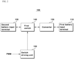
- FIG. 2 is a block diagram of a battery switch driving circuit according to an embodiment of the present invention.
- the battery switch driving circuit 100 comprises a first battery input terminal 110, a second battery input terminal 120, a converter 130, a first switch 140, and a switch driving unit 150, and may include a second switch 151, a first capacitor 152, a second capacitor 153, and resistors and diodes being connected between each component.
- the first battery input terminal 110 is connected to a first battery (not shown) having a first battery voltage, and may receive the first battery voltage or output a voltage to the first battery to charge the first battery.
- the second battery input terminal 120 is connected to a second battery (not shown) having a second battery voltage that is different from that of the first battery input terminal 110, and receives the second battery voltage or may charge the second battery by outputting a voltage to the second battery.
- the first battery may be a low voltage battery, for example a 12 V battery
- the first battery may be a high voltage battery, for example a 48 V battery.
- the first battery may be a high voltage battery and the second battery is a low voltage battery, or may be batteries of the same voltage.
- the converter 130 is located between the first battery input terminal 110 and the second battery input terminal 120, converts the first battery voltage being inputted to the first battery input terminal 110 into a second battery voltage to output it to the second battery input terminal 120, or may convert the second battery voltage being inputted to the second battery input terminal 120 into a first battery voltage to output it to the first battery input terminal 110.
- the converter 130 may be a bi-directional converter being configured with a plurality of switches and an inductor, and may perform charging between different batteries through the converter.
- the first switch 140 is located between the second battery input terminal and the converter, and blocks power input of the second battery input terminal 120 when turned off.
- the second battery voltage connected to the second battery input terminal 120 may be greater than the first battery voltage connected to the first battery input terminal 110, and the second battery voltage is received and converted into the first battery voltage through the converter 130 to charge the first battery connected to the first battery input terminal 110 or may supply power to devices receiving power from the first battery.
- the first switch 140 is turned on, and other than that, the first switch 140 is turned off so that the second battery voltage is not applied to the first battery.
- power input of the second battery input terminal 120 may be released from blocking.
- the switch driving unit 150 turns a first switch 140 on. In order to turn the first switch 140 on and off, driving power must be supplied to the first switch 140, and the switch driving unit 150 supplies driving power to the first switch 140 to turn it on.
- the switch driver may comprise a second switch 151, a first capacitor 152, and a second capacitor 153. It may include a first capacitor 152 being charged and discharged according to the on-off of the second switch 151 being operated with a PWM signal, and a second capacitor 153 being charged according to the on-off of the second switch 151 by the voltage being charged in the first capacitor 152.
- One end of the first capacitor 152 is connected to the first battery input terminal 110 and the other end thereof may be connected to the second switch 151.
- the second switch 151 When the second switch 151 is turned on by a PWM signal, a path through which current flows to the first battery input terminal 110, the first capacitor 152, and the second switch 151 is connected so that the first capacitor 152 may be charged by current flowing from the first battery input terminal 110.
- the first capacitor 152 may be connected to the first battery input terminal 110 through a first resistor R1 and a first diode D1. A current may be allowed to flow through the first resistor R1, and current may be prevented from flowing in a reverse direction when the second switch 151 is turned off through the first diode D1.
- One end the first capacitor 152 is connected to the system power input terminal (not shown) or the second battery input terminal 120 and the other end thereof may be connected to the second switch 151. As shown in FIG. 3 , the first capacitor 152 is not connected to the first battery input terminal 110, but is connected to the system power input terminal or the second battery input terminal 120 so that it can be charged through the system power input terminal or the second battery voltage.
- the first capacitor 152 when one end of the first capacitor 152 is connected to the second battery input terminal 120, it may include a clamping circuit (not shown) clamping the voltage being inputted from the second battery input terminal 120 to the first battery voltage.
- the second battery may have a high voltage as a high side, and when a high voltage is used, the size of the rated voltage of the device should be increased, so when using high voltage, a clamping circuit that lowers the second battery voltage to the first battery voltage or a preset voltage may be formed.
- a clamping circuit that lowers the second battery voltage to the first battery voltage or a preset voltage may be formed.
- the clamping circuit it is possible to receive a high voltage and drive the battery switch driving circuit with a low voltage, and thus, it is possible to implement a circuit using low-cost devices.
- One end the first capacitor 152 is connected to one end of the second capacitor 153 and the other end thereof may be connected to the other end of the second capacitor 153.
- the second switch 151 When the second switch 151 is turned off by a PWM signal, the path through which current flows through the second switch 151 is disconnected, and the first capacitor 152 and the second capacitor 153 form a closed loop with each other. Through this, the voltage charged in the first capacitor 152 charges the second capacitor 153.
- the other end of the first capacitor 152 is connected to the other end of the second capacitor 153 through a second resistor R2 and a second diode D2, and one end of the first capacitor 152 may be connected to one end of the second capacitor 153 through a third resistor RG and a third diode D3.
- a current may flow through the second resistor R2 and the third resistor RG, and a current may flow in a direction in which the first capacitor 152 charges the second capacitor 153 through the second diode D2 and the third diode D3.
- the first switch 140 may be a MOSFET, one end of the second capacitor 153 is connected to the gate of the first switch 140 and the other end thereof is connected to the source so that the first switch 140 may be turned on when it is charged above the gate threshold value of the first switch 140. Both ends of the second capacitor 153 may be connected to the gate terminal and the source terminal of the first switch 140, respectively. That is, the voltage being charged in the second capacitor 153 becomes the gate-source voltage of the first switch 140. The first switch 140 is turned on when the gate-source voltage exceeds the threshold value so that the first switch 140 is turned on when the voltage being charged in the second capacitor 153 exceeds the threshold value.
- the battery switch can be driven using only the switch, capacitor, diode, and resistor, a battery switch driving circuit advantageous in terms of price and size can be implemented.
- FIG. 4 is a circuit diagram of a battery switch driving circuit according to an embodiment of the present invention.
- a 12 V battery may be connected to the first battery input terminal, and a 48 V battery may be connected to the second battery input terminal.
- the converter may be a DC-DC converter and may be a bi-directional converter formed of two switches Q1 and Q2 and an inductor L.
- the first switch SW1 is formed between the 48 V battery and the DC-DC converter.
- the switch driver driving the first switch SW1, as shown in FIG. 4 may comprise: a first capacitor C1 being connected to a 12 V battery through a second switch SW2 operated by a PWM signal, a first resistor R1 and a first diode D1; and a second capacitor CG having both ends connected to the first capacitor C1.
- the first capacitor C1 and the second capacitor CG may be connected through the second resistor R2 and the second diode D2, the third resistor RG, and the second diode D3. Both ends of the second capacitor CG may be connected to the gate and source of the first switch SW1 and the other end of the second capacitor 153 may be connected to a DC-DC converter.
- the battery switch driving circuit of FIG. 4 may operate as shown in FIGS. 5 and 6 according to a PWM signal.
- the leakage current flows through L and Q1 of the DC-DC converter, the second resistor R2, the second diode D2, the second switch SW2, and path P2 as shown in the following equation, and since this value is a loss, the value of the second resistor R2 should be selected with an appropriately large value.
- I leakage 12 V battery ⁇ V ⁇ , D 2 ⁇ V ⁇ , Q 1 / R L , DCR + R SW 2 , RDC + R 2
- the size of the second resistor R2 may be set according to an allowable leakage current allowed by the battery device or system, and may be set by a user.
- the second resistor R2 may have a larger size than the first resistor R1 and the third resistor RG.
- V C 1 ⁇ GND V C 1 , charged + 12 V battery ⁇ V ⁇ , D 2 ⁇ V ⁇ , Q 1
- the voltage charged in the first capacitor C1 charges the second capacitor CG through the third diode D3, the third resistor RG, the second capacitor RG, the first resistor R2, the second diode D2, and the path P3, and a voltage is charged in the second capacitor CG to turn the first switch SW1 on.
- V Cg 12 V battery ⁇ V ⁇ , D 1 ⁇ V ⁇ , D 2 ⁇ V ⁇ , D 3
- the first switch SW1 When the voltage across the second capacitor CG exceeds the threshold value of the gate of the first switch SW1, the first switch SW1 is turned on, and the source voltage of the first switch SW1 rises to 48 V battery voltage from 12 V battery voltage.
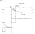
- FIG. 7 is a circuit in which simulation of FIG. 4 is performed, and FIG. 8 shows the result of the simulation.
- FIG. 8 shows the result of the simulation.
- the first switch 140 located between the first battery input terminal 110 and the converter 130 and blocking the power input of the second battery input terminal 120 when off, is located between the first battery input terminal 110 and the converter 130 instead, may include a fourth switch and a fifth switch that block power input in opposite directions when turned off may be included.
- the switch driver 150 may turn on the fourth switch and the fifth switch.
- the switch structure can be implemented as a back-to-back structure by using the fourth switch and the fifth switch capable of blocking bi-directional power input instead of the first switch 140.
- the back-to-back structure means a structure that blocks bi-directional signal input.
- the second capacitor 153 of the switch driver 150 is connected to the gate and drain of the back-to-back structure switch being formed of the fourth switch and the fifth switch, and as described above, the fourth switch and the fifth switch may be turned on.
- FIG. 9 is a circuit diagram of a battery switch driving circuit according to another embodiment of the present invention.
- a battery switch can be implemented in a back-to-back structure by connecting two switches in opposite directions.
- the battery switch driving circuit of FIG. 9 as in the battery switch driving circuit of FIG. 4 , when a PWM signal is applied to the second switch SW2, the first capacitor C1 is charged, and the second capacitor CG is charged so that the fourth and fifth switches are turned on and operate.
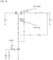
- FIG. 10 is a circuit in which simulation of FIG. 9 is performed, and FIG. 11 shows a result of the simulation.
- a PWM signal is applied, and the gate-source voltage SW1_V GS of the switch SW1 of the back-to-back structure of the fourth switch and the fifth switch starts to be charged, and when the voltage exceeds the threshold value of the gate of the first switch SW1, the first switch SW1 is turned on, and it can be confirmed that the drain voltage SW1_ DRAIN of the first switch SW1 rises from the 12 V battery voltage to the 48 V battery voltage.
- a switch-off circuit may be included to quickly turn off the first switch SW1 in an emergency situation or the like.
- the optocoupler is a switch operated by light, and is composed of a light emitting diode that emits light when current flows and a switch that is turned on by light emitted from the light emitting diode.
- the third switch SW3 When the first switch-off signal is applied to the gate of the third switch SW3, the third switch SW3 is turned on and light is emitted from the light emitting diode of the optocoupler to operate the optocoupler, and the voltage charged in the second capacitor 153 is quickly discharged by forming a closed loop with the second capacitor 153 to quickly turn the first switch 140 on.
- FIG. 2 is a circuit diagram of a battery switch driving circuit according to another embodiment of the present invention, which can quickly turn on and off the first switch SW1.
- the battery switch driving circuit of FIG. 12 operates like the battery switch driving circuit of FIG. 4 when the first switch SW1 is turned on, but when the first switch SW1 is turned off, a switch-off circuit is driven as shown in FIG. 13 .
- the first switch-off signal SWITCH-OFF is applied to the third switch SW3
- the third switch SW3 is turned on, and the optocoupler is turned on by the 12 V battery voltage, the light emitting diode of the optocoupler, the fourth resistor R3, and the path P4.
- the third resistor RG may include a fifth resistor RG1 and a sixth resistor RG2, and when the optocoupler is turned on, the second capacitor CG is quickly discharged by the optocoupler, the fifth resistor RG1, the second capacitor CG, and the path P5, and accordingly, the first switch SW1 is quickly turned off.
- the voltage of the second capacitor CG being discharged is as follows.
- V Cg 12 V battery ⁇ V ⁇ , D 1 ⁇ V ⁇ , D 2 ⁇ V ⁇ , D 3 e ⁇ 1 CgRg 1 l
- FIG. 14 is a circuit in which simulation of FIG. 12 is performed, and FIG. 15 illustrates the result of the simulation.
- the optocoupler is turned on, and the gate-source voltage SW1_V GS of the first switch SW1 starts to discharge, and the first switch SW1 is turned off when the voltage is less than the threshold value of the gate of the first switch SW1, and it can be confirmed that the source voltage SW1_SOURCE of the first switch SW1 drops from the 48 V battery voltage to the 12 V battery voltage.
- the high side switch can be turned on and off by implementing a battery switch driving circuit with capacitors, diodes, resistors, and switches.
- the switch configured in back-to-back can be turned on and off by using another battery switch driving circuit according to the embodiment of the present invention, and other than this, various types of semiconductor switches (FET, IGBT, etc.) can be turned on and off.
- the battery switch can be quickly turned off through the switch-off circuit.
Landscapes
- Engineering & Computer Science (AREA)
- Power Engineering (AREA)
- Electronic Switches (AREA)
- Charge And Discharge Circuits For Batteries Or The Like (AREA)
Abstract
Description
- The present invention relates to a battery switch driving circuit, and more particularly, to a battery switch driving circuit for driving a battery switch using a switch, a capacitor, and a diode.
- Recently, pluralities of batteries are used instead of a single battery, and battery application fields using a specific battery according to circumstances are increasing. For example, it is applied to various fields such as automobiles, automation devices, medical devices, and robots.
-
FIG. 1 is a system using a 48 V battery and a 12 V battery, and a 48 V battery can be charged using a 12 V battery or a 12 V battery can be charged using a 48 V battery through a DC-DC converter. In the case of using a 12 V battery, a semiconductor switch (FET, IGBT) may be used to disconnect and isolate the 48 V battery. - In order to turn on/off a semiconductor switch located on a high side, which is a high voltage, a high side switch driving unit for driving the semiconductor switch is required, as shown in
FIG. 1 , and the gate power of the semiconductor switch can be made with a push-pull method applying an isolation transformer, and the switch can be turned on with that power. - A circuit for driving such a high side semiconductor switch requires a buffer that amplifies a PWM signal and a transformer for isolation, and because of this, there are disadvantages in that product price increases and product size increases.
- A technical problem to be solved by the present invention is to provide a battery switch driving circuit for driving a battery switch using a switch, a capacitor, and a diode.
- A battery switch driving circuit according to an embodiment of the present invention comprises: a first battery input terminal and a second battery input terminal; a converter positioned between the first battery input terminal and the second battery input terminal; a first switch positioned between the second battery input terminal and the converter, so as to cut off a power input of the second battery input terminal when turned off; and a switch driving unit for turning on the first switch, wherein the switch driving unit comprises: a first capacitor which is charged or discharged according to on/off of a second switch operated by a PWM signal; and a second capacitor which is charged according to on/off of the second switch by a voltage charged in the first capacitor, so as to turn on the first switch.
- In addition, one end of the first capacitor is connected to the first battery input terminal and the other end thereof may be connected to the second switch.
- In addition, the first capacitor may be connected to the first battery input terminal through a first resistor and a first diode.
- In addition, one end of the first capacitor is connected to one end of the second capacitor and the other end thereof may be connected to the other end of the second capacitor.
- In addition, the other end of the first capacitor is connected to the other end of the second capacitor through a second resistor and a second diode, and one end of the first capacitor may be connected to one end of the second capacitor through a third resistor and a third diode.
- In addition, one end of the second capacitor is connected to the gate of the first switch and the other end thereof is connected to the source, and the first switch may be turned on when it is charged above a gate threshold value of the first switch.
- In addition, one end of the first capacitor is connected to the system power input terminal or the second battery input terminal, and the other end thereof may be connected to the second switch.
- In addition, when one end of the first capacitor is connected to the second battery input terminal, a clamping circuit for clamping a voltage being inputted from the second battery input terminal to a first battery voltage may be included.
- In addition, it includes a third switch being connected to the first battery input terminal through an optocoupler and a fourth resistor and being turned on and off according to the first switch off signal, wherein the optocoupler forms a closed loop with the second capacitor, but it is operated when the third switch is turned on, so that the voltage of the second capacitor can be discharged.
- In order to solve the above technical problem, a battery switch driving circuit according to another embodiment of the present invention comprises: a first battery input terminal; a second battery input terminal having a different battery voltage from the first battery input terminal; a converter positioned between the first battery input terminal and the second battery input terminal; a fourth switch and a fifth switch positioned between the second battery input terminal and the converter to block power input in opposite directions when turned off; and a switch driving unit for turning on the fourth switch and the fifth switch, wherein the switch driving unit includes a first capacitor being charged and discharged according to the on/off of the second switch being operated with a PWM signal; and a second capacitor being charged according to the on/off of the second switch by the voltage being charged in the first capacitor to turn on the fourth switch or the fifth switch.
- According to embodiments of the present invention, driving a semiconductor switch using a switch, a capacitor, and a diode is advantageous in terms of price and size. In addition, it can be configured in a back-to-back configuration, and the switch can be turned off quickly when necessary.
-
-
FIG. 1 illustrates a battery switch driving circuit according to a comparative embodiment of the present invention. -
FIG. 2 is a block diagram of a battery switch driving circuit according to an embodiment of the present invention. -
FIG. 3 is a block diagram of a battery switch driving circuit according to an embodiment of the present invention. -
FIG. 4 is a circuit diagram of a battery switch driving circuit according to an embodiment of the present invention. -
FIGS. 5 to 8 are diagrams for explaining the operation of the embodiment ofFIG. 4 . -
FIG. 9 is a circuit diagram of a battery switch driving circuit according to another embodiment of the present invention. -
FIGS. 10 and11 are diagrams for explaining the operation of the embodiment ofFIG. 9 . -
FIG. 12 is a circuit diagram of a battery switch driving circuit according to another embodiment of the present invention. -
FIGS. 13 to 15 are views for explaining the operation of the embodiment ofFIG. 12 . - Hereinafter, preferred embodiments of the present invention will be described in detail with reference to the accompanying drawings.
- However, the technical idea of the present invention is not limited to some embodiments to be described, but may be implemented in various forms, and inside the scope of the technical idea of the present invention, one or more of the constituent elements may be selectively combined or substituted between embodiments.
- In addition, the terms (including technical and scientific terms) used in the embodiments of the present invention, unless explicitly defined and described, can be interpreted as a meaning that can be generally understood by a person skilled in the art, and commonly used terms such as terms defined in the dictionary may be interpreted in consideration of the meaning of the context of the related technology.
- In addition, terms used in the present specification are for describing embodiments and are not intended to limit the present invention.
- In the present specification, the singular form may include the plural form unless specifically stated in the phrase, and when described as "at least one (or more than one) of A and B and C", it may include one or more of all combinations that can be combined with A, B, and C.
- In addition, in describing the components of the embodiment of the present invention, terms such as first, second, A, B, (a), and (b) may be used. These terms are merely intended to distinguish the components from other components, and the terms do not limit the nature, order or sequence of the components.
- And, when a component is described as being 'connected', 'coupled' or 'interconnected' to another component, the component is not only directly connected, coupled or interconnected to the other component, but may also include cases of being 'connected', 'coupled', or 'interconnected' due that another component between that other components.
- In addition, when described as being formed or arranged in "on (above)" or "below (under)" of each component, "on (above)" or "below (under)" means that it includes not only the case where the two components are directly in contact with, but also the case where one or more other components are formed or arranged between the two components. In addition, when expressed as "on (above)" or "below (under)", the meaning of not only an upward direction but also a downward direction based on one component may be included.
-
FIG. 2 is a block diagram of a battery switch driving circuit according to an embodiment of the present invention. - The battery
switch driving circuit 100 according to an embodiment of the present invention comprises a firstbattery input terminal 110, a secondbattery input terminal 120, aconverter 130, afirst switch 140, and aswitch driving unit 150, and may include asecond switch 151, afirst capacitor 152, asecond capacitor 153, and resistors and diodes being connected between each component. - The first
battery input terminal 110 is connected to a first battery (not shown) having a first battery voltage, and may receive the first battery voltage or output a voltage to the first battery to charge the first battery. The secondbattery input terminal 120 is connected to a second battery (not shown) having a second battery voltage that is different from that of the firstbattery input terminal 110, and receives the second battery voltage or may charge the second battery by outputting a voltage to the second battery. Here, the first battery may be a low voltage battery, for example a 12 V battery, and the first battery may be a high voltage battery, for example a 48 V battery. Or, the first battery may be a high voltage battery and the second battery is a low voltage battery, or may be batteries of the same voltage. - The
converter 130 is located between the firstbattery input terminal 110 and the secondbattery input terminal 120, converts the first battery voltage being inputted to the firstbattery input terminal 110 into a second battery voltage to output it to the secondbattery input terminal 120, or may convert the second battery voltage being inputted to the secondbattery input terminal 120 into a first battery voltage to output it to the firstbattery input terminal 110. Theconverter 130 may be a bi-directional converter being configured with a plurality of switches and an inductor, and may perform charging between different batteries through the converter. - The
first switch 140 is located between the second battery input terminal and the converter, and blocks power input of the secondbattery input terminal 120 when turned off. The second battery voltage connected to the secondbattery input terminal 120 may be greater than the first battery voltage connected to the firstbattery input terminal 110, and the second battery voltage is received and converted into the first battery voltage through theconverter 130 to charge the first battery connected to the firstbattery input terminal 110 or may supply power to devices receiving power from the first battery. In a situation where the second battery voltage is input and used, thefirst switch 140 is turned on, and other than that, thefirst switch 140 is turned off so that the second battery voltage is not applied to the first battery. When thefirst switch 140 is turned off, power input of the secondbattery input terminal 120 may be released from blocking. - The
switch driving unit 150 turns afirst switch 140 on. In order to turn thefirst switch 140 on and off, driving power must be supplied to thefirst switch 140, and theswitch driving unit 150 supplies driving power to thefirst switch 140 to turn it on. - As shown in
FIG. 3 , the switch driver may comprise asecond switch 151, afirst capacitor 152, and asecond capacitor 153. It may include afirst capacitor 152 being charged and discharged according to the on-off of thesecond switch 151 being operated with a PWM signal, and asecond capacitor 153 being charged according to the on-off of thesecond switch 151 by the voltage being charged in thefirst capacitor 152. - One end of the
first capacitor 152 is connected to the firstbattery input terminal 110 and the other end thereof may be connected to thesecond switch 151. When thesecond switch 151 is turned on by a PWM signal, a path through which current flows to the firstbattery input terminal 110, thefirst capacitor 152, and thesecond switch 151 is connected so that thefirst capacitor 152 may be charged by current flowing from the firstbattery input terminal 110. Here, thefirst capacitor 152 may be connected to the firstbattery input terminal 110 through a first resistor R1 and a first diode D1. A current may be allowed to flow through the first resistor R1, and current may be prevented from flowing in a reverse direction when thesecond switch 151 is turned off through the first diode D1. - One end the
first capacitor 152 is connected to the system power input terminal (not shown) or the secondbattery input terminal 120 and the other end thereof may be connected to thesecond switch 151. As shown inFIG. 3 , thefirst capacitor 152 is not connected to the firstbattery input terminal 110, but is connected to the system power input terminal or the secondbattery input terminal 120 so that it can be charged through the system power input terminal or the second battery voltage. Here, when one end of thefirst capacitor 152 is connected to the secondbattery input terminal 120, it may include a clamping circuit (not shown) clamping the voltage being inputted from the secondbattery input terminal 120 to the first battery voltage. As described above, the second battery may have a high voltage as a high side, and when a high voltage is used, the size of the rated voltage of the device should be increased, so when using high voltage, a clamping circuit that lowers the second battery voltage to the first battery voltage or a preset voltage may be formed. Through the clamping circuit, it is possible to receive a high voltage and drive the battery switch driving circuit with a low voltage, and thus, it is possible to implement a circuit using low-cost devices. - One end the
first capacitor 152 is connected to one end of thesecond capacitor 153 and the other end thereof may be connected to the other end of thesecond capacitor 153. When thesecond switch 151 is turned off by a PWM signal, the path through which current flows through thesecond switch 151 is disconnected, and thefirst capacitor 152 and thesecond capacitor 153 form a closed loop with each other. Through this, the voltage charged in thefirst capacitor 152 charges thesecond capacitor 153. Here, the other end of thefirst capacitor 152 is connected to the other end of thesecond capacitor 153 through a second resistor R2 and a second diode D2, and one end of thefirst capacitor 152 may be connected to one end of thesecond capacitor 153 through a third resistor RG and a third diode D3. A current may flow through the second resistor R2 and the third resistor RG, and a current may flow in a direction in which thefirst capacitor 152 charges thesecond capacitor 153 through the second diode D2 and the third diode D3. - The
first switch 140 may be a MOSFET, one end of thesecond capacitor 153 is connected to the gate of thefirst switch 140 and the other end thereof is connected to the source so that thefirst switch 140 may be turned on when it is charged above the gate threshold value of thefirst switch 140. Both ends of thesecond capacitor 153 may be connected to the gate terminal and the source terminal of thefirst switch 140, respectively. That is, the voltage being charged in thesecond capacitor 153 becomes the gate-source voltage of thefirst switch 140. Thefirst switch 140 is turned on when the gate-source voltage exceeds the threshold value so that thefirst switch 140 is turned on when the voltage being charged in thesecond capacitor 153 exceeds the threshold value. - As described above, since the battery switch can be driven using only the switch, capacitor, diode, and resistor, a battery switch driving circuit advantageous in terms of price and size can be implemented.
-
FIG. 4 is a circuit diagram of a battery switch driving circuit according to an embodiment of the present invention. A 12 V battery may be connected to the first battery input terminal, and a 48 V battery may be connected to the second battery input terminal. The converter may be a DC-DC converter and may be a bi-directional converter formed of two switches Q1 and Q2 and an inductor L. The first switch SW1 is formed between the 48 V battery and the DC-DC converter. The switch driver driving the first switch SW1, as shown inFIG. 4 , may comprise: a first capacitor C1 being connected to a 12 V battery through a second switch SW2 operated by a PWM signal, a first resistor R1 and a first diode D1; and a second capacitor CG having both ends connected to the first capacitor C1. The first capacitor C1 and the second capacitor CG may be connected through the second resistor R2 and the second diode D2, the third resistor RG, and the second diode D3. Both ends of the second capacitor CG may be connected to the gate and source of the first switch SW1 and the other end of thesecond capacitor 153 may be connected to a DC-DC converter. - The battery switch driving circuit of
FIG. 4 may operate as shown inFIGS. 5 and6 according to a PWM signal. - In the state where the first switch SW1 is off, 12
V battery voltage 12Vbattery is applied to the source of the first switch SW1 through Q1 and L of the DC-DC converter, so that the source voltage of the first switch SW1 becomes 12Vbattery - Vf,Q1. When a PWM signal is applied to the gate of the second switch SW2 to turn the first switch SW1 on, the second switch SW2 repeats on/off. - When the second switch SW2 is turned on by a PWM signal, the
12V battery voltage 12Vbattery charges the first capacitor C1 through the first diode D1, the first resistor R1, and path P1. At this time, the voltage of the first capacitor VC1 rises as follows.
- In addition, the leakage current flows through L and Q1 of the DC-DC converter, the second resistor R2, the second diode D2, the second switch SW2, and path P2 as shown in the following equation, and since this value is a loss, the value of the second resistor R2 should be selected with an appropriately large value.

- Here, the size of the second resistor R2 may be set according to an allowable leakage current allowed by the battery device or system, and may be set by a user. The second resistor R2 may have a larger size than the first resistor R1 and the third resistor RG.
- As shown in
FIG. 6 , when the second switch SW2 is turned off by a PWM signal, the voltage of the first capacitor C1 is greater than the 12 V battery voltage and the first diode D1 is turned off.
- The voltage charged in the first capacitor C1 charges the second capacitor CG through the third diode D3, the third resistor RG, the second capacitor RG, the first resistor R2, the second diode D2, and the path P3, and a voltage is charged in the second capacitor CG to turn the first switch SW1 on.
- When the second switch SW2 repeats on/off by a PWM signal, the first capacitor C1 is charged while the second switch SW2 is turned on; the gate voltage of the first switch SW1 rises by charging the second capacitor CG with the voltage charged in the first capacitor C1 when the second switch SW2 is off; and as a result, the voltage across the second capacitor CG becomes as follows.

- When the voltage across the second capacitor CG exceeds the threshold value of the gate of the first switch SW1, the first switch SW1 is turned on, and the source voltage of the first switch SW1 rises to 48 V battery voltage from 12 V battery voltage.
-
FIG. 7 is a circuit in which simulation ofFIG. 4 is performed, andFIG. 8 shows the result of the simulation. As a result of the simulation, when a PWM signal is applied and the gate-source voltage SW1_Vgs of the first switch SW1 starts to be charged, and the voltage exceeds the threshold value of the gate of the first switch SW1 to turn the first switch SW1 on and it can be confirmed that the source voltage SW1_SOURCE of the first switch SW1 rises from the 12 V battery voltage to the 48 V battery voltage. - The
first switch 140, located between the firstbattery input terminal 110 and theconverter 130 and blocking the power input of the secondbattery input terminal 120 when off, is located between the firstbattery input terminal 110 and theconverter 130 instead, may include a fourth switch and a fifth switch that block power input in opposite directions when turned off may be included. At this time, theswitch driver 150 may turn on the fourth switch and the fifth switch. The switch structure can be implemented as a back-to-back structure by using the fourth switch and the fifth switch capable of blocking bi-directional power input instead of thefirst switch 140. Here, the back-to-back structure means a structure that blocks bi-directional signal input. Thesecond capacitor 153 of theswitch driver 150 is connected to the gate and drain of the back-to-back structure switch being formed of the fourth switch and the fifth switch, and as described above, the fourth switch and the fifth switch may be turned on. -
FIG. 9 is a circuit diagram of a battery switch driving circuit according to another embodiment of the present invention. A battery switch can be implemented in a back-to-back structure by connecting two switches in opposite directions. In the battery switch driving circuit ofFIG. 9 , as in the battery switch driving circuit ofFIG. 4 , when a PWM signal is applied to the second switch SW2, the first capacitor C1 is charged, and the second capacitor CG is charged so that the fourth and fifth switches are turned on and operate. -
FIG. 10 is a circuit in which simulation ofFIG. 9 is performed, andFIG. 11 shows a result of the simulation. As the result of the simulation, a PWM signal is applied, and the gate-source voltage SW1_VGS of the switch SW1 of the back-to-back structure of the fourth switch and the fifth switch starts to be charged, and when the voltage exceeds the threshold value of the gate of the first switch SW1, the first switch SW1 is turned on, and it can be confirmed that the drain voltage SW1_DRAIN of the first switch SW1 rises from the 12 V battery voltage to the 48 V battery voltage. - In order to turn off the first switch SW1 while the first switch SW1 is on, the voltage charged in the second capacitor CG must be discharged, so a switch-off circuit may be included to quickly turn off the first switch SW1 in an emergency situation or the like.
- To this end, it is connected to the first battery input terminal through an optocoupler and a fourth resistor R3 and includes a third switch SW3 which is turned on and off according to the off signal of the first switch, the optocoupler forms a closed loop with the
second capacitor 153, and the voltage of thesecond capacitor 153 can be discharged as it is operated when the third switch SW3 is turned on. Here, the optocoupler is a switch operated by light, and is composed of a light emitting diode that emits light when current flows and a switch that is turned on by light emitted from the light emitting diode. When the first switch-off signal is applied to the gate of the third switch SW3, the third switch SW3 is turned on and light is emitted from the light emitting diode of the optocoupler to operate the optocoupler, and the voltage charged in thesecond capacitor 153 is quickly discharged by forming a closed loop with thesecond capacitor 153 to quickly turn thefirst switch 140 on. -
FIG. 2 is a circuit diagram of a battery switch driving circuit according to another embodiment of the present invention, which can quickly turn on and off the first switch SW1. The battery switch driving circuit ofFIG. 12 operates like the battery switch driving circuit ofFIG. 4 when the first switch SW1 is turned on, but when the first switch SW1 is turned off, a switch-off circuit is driven as shown inFIG. 13 . When the first switch-off signal SWITCH-OFF is applied to the third switch SW3, the third switch SW3 is turned on, and the optocoupler is turned on by the 12 V battery voltage, the light emitting diode of the optocoupler, the fourth resistor R3, and the path P4. The third resistor RG may include a fifth resistor RG1 and a sixth resistor RG2, and when the optocoupler is turned on, the second capacitor CG is quickly discharged by the optocoupler, the fifth resistor RG1, the second capacitor CG, and the path P5, and accordingly, the first switch SW1 is quickly turned off. Here, the voltage of the second capacitor CG being discharged is as follows.
-
FIG. 14 is a circuit in which simulation ofFIG. 12 is performed, andFIG. 15 illustrates the result of the simulation. As the result of the simulation, when the first switch-off signal SWITCH-OFF is applied and the third switch is turned on, the optocoupler is turned on, and the gate-source voltage SW1_VGS of the first switch SW1 starts to discharge, and the first switch SW1 is turned off when the voltage is less than the threshold value of the gate of the first switch SW1, and it can be confirmed that the source voltage SW1_SOURCE of the first switch SW1 drops from the 48 V battery voltage to the 12 V battery voltage. - As described above, the high side switch can be turned on and off by implementing a battery switch driving circuit with capacitors, diodes, resistors, and switches. In addition, the switch configured in back-to-back can be turned on and off by using another battery switch driving circuit according to the embodiment of the present invention, and other than this, various types of semiconductor switches (FET, IGBT, etc.) can be turned on and off. In addition, the battery switch can be quickly turned off through the switch-off circuit.
- Those skilled in the art related to the present embodiment will be able to understand that it can be implemented in a modified form within a range that does not deviate from the essential characteristics of the above description. Therefore, the disclosed methods are to be considered in an illustrative rather than a limiting sense. The scope of the present invention is shown in the claims rather than the foregoing description, and all differences within the equivalent scope will be construed as being included in the present invention.
Claims (10)
- A battery switch driving circuit comprising:a first battery input terminal and a second battery input terminal;a converter positioned between the first battery input terminal and the second battery input terminal;a first switch positioned between the second battery input terminal and the converter, configured to cut off a power input of the second battery input terminal when turned off; anda switch driving unit configured to turn on the first switch,wherein the switch driving unit comprises:a first capacitor charged or discharged according to on/off of a second switch operated by a PWM signal; anda second capacitor charged according to on/off of the second switch by a voltage charged in the first capacitor, and configured to turn on the first switch.
- The battery switch driving circuit according to claim 1,
wherein one end of the first capacitor is connected to the first battery input terminal and the other end thereof is connected to the second switch. - The battery switch driving circuit according to claim 2,
wherein the first capacitor is connected to the first battery input terminal through a first resistor and a first diode. - The battery switch driving circuit according to claim 1,
wherein one end of the first capacitor is connected to one end of the second capacitor and the other end thereof is connected to the other end of the second capacitor. - The battery switch driving circuit according to claim 4,wherein the other end of the first capacitor is connected to the other end of the second capacitor through a second resistor and a second diode, andwherein one end of the first capacitor is connected to one end of the second capacitor through a third resistor and a third diode.
- The battery switch driving circuit according to claim 1,wherein one end of the second capacitor is connected to a gate of the first switch and the other end thereof is connected to a source, andwherein the first switch is turned on when it is charged above a gate threshold value of the first switch.
- The battery switch driving circuit according to claim 1,
wherein one end of the first capacitor is connected to a system power input terminal or the second battery input terminal, and the other end thereof is connected to the second switch. - The battery switch driving circuit according to claim 7 comprising:
a clamping circuit configured to clamp a voltage inputted from the second battery input terminal to a first battery voltage when one end of the first capacitor is connected to the second battery input terminal. - The battery switch driving circuit according to claim 1 comprising:a third switch connected to the first battery input terminal through an optocoupler and a fourth resistor, and turned on and off according to off signal of the first switch,wherein the optocoupler forms a closed loop with the second capacitor and operates when the third switch is turned on, so that the voltage of the second capacitor is discharged.
- A battery switch driving circuit comprising:a first battery input terminal and a second battery input terminal;a converter positioned between the first battery input terminal and the second battery input terminal;a fourth switch and a fifth switch positioned between the second battery input terminal and the converter, and configured to block power input in opposite directions when turned off; anda switch driving unit configured to turn on the fourth switch and the fifth switch,wherein the switch driving unit comprises:a first capacitor charged and discharged according to on/off of a second switch operated by a PWM signal; anda second capacitor charged according to on/off of the second switch by the voltage charged in the first capacitor, and configured to turn on the fourth switch or the fifth switch.
Applications Claiming Priority (2)
| Application Number | Priority Date | Filing Date | Title |
|---|---|---|---|
| KR1020210012390A KR102912840B1 (en) | 2021-01-28 | 2021-01-28 | Battery switch driving circuit |
| PCT/KR2022/001262 WO2022164164A1 (en) | 2021-01-28 | 2022-01-24 | Battery switch driving circuit |
Publications (2)
| Publication Number | Publication Date |
|---|---|
| EP4287478A1 true EP4287478A1 (en) | 2023-12-06 |
| EP4287478A4 EP4287478A4 (en) | 2024-12-04 |
Family
ID=82654004
Family Applications (1)
| Application Number | Title | Priority Date | Filing Date |
|---|---|---|---|
| EP22746191.0A Pending EP4287478A4 (en) | 2021-01-28 | 2022-01-24 | Battery switch driving circuit |
Country Status (5)
| Country | Link |
|---|---|
| US (1) | US12348128B2 (en) |
| EP (1) | EP4287478A4 (en) |
| JP (1) | JP7802810B2 (en) |
| KR (1) | KR102912840B1 (en) |
| WO (1) | WO2022164164A1 (en) |
Families Citing this family (1)
| Publication number | Priority date | Publication date | Assignee | Title |
|---|---|---|---|---|
| US12531410B2 (en) * | 2021-11-03 | 2026-01-20 | Lg Energy Solution, Ltd. | Battery rack management apparatus and method for operating same |
Family Cites Families (11)
| Publication number | Priority date | Publication date | Assignee | Title |
|---|---|---|---|---|
| US4737667A (en) | 1986-03-11 | 1988-04-12 | Siemens Aktiengesellschaft | Driving circuitry for a MOSFET having a source load |
| JP3289680B2 (en) | 1998-06-05 | 2002-06-10 | 日本電気株式会社 | Power supply inrush current prevention circuit |
| JP4138664B2 (en) * | 2002-01-22 | 2008-08-27 | ジョンソン コントロールズ オートモーティブ エレクトロニクス | Multi-cellular DC / DC voltage converter with protection switch |
| JP5842483B2 (en) | 2011-09-06 | 2016-01-13 | 株式会社デンソー | Secondary battery power supply device and in-vehicle device |
| KR101395041B1 (en) * | 2012-10-05 | 2014-05-16 | (주)한국엘에스아이 | Switching Charger Device |
| KR102131582B1 (en) * | 2013-10-21 | 2020-08-06 | 현대모비스 주식회사 | Motor drive apparatus |
| JP2016140118A (en) | 2015-01-26 | 2016-08-04 | 株式会社村田製作所 | Power supply |
| CN107408884B (en) * | 2015-03-31 | 2020-03-17 | 古河电气工业株式会社 | Power conversion device and control method for power conversion device |
| JP6436055B2 (en) * | 2015-10-28 | 2018-12-12 | 株式会社オートネットワーク技術研究所 | Multiphase converter |
| CN106027013B (en) | 2016-06-23 | 2020-05-12 | 昂宝电子(上海)有限公司 | Control device and control method for analog power switch |
| FR3090226B1 (en) * | 2018-12-17 | 2021-03-19 | Valeo Systemes De Controle Moteur | DC / DC voltage converter including a safety device |
-
2021
- 2021-01-28 KR KR1020210012390A patent/KR102912840B1/en active Active
-
2022
- 2022-01-24 EP EP22746191.0A patent/EP4287478A4/en active Pending
- 2022-01-24 JP JP2023546133A patent/JP7802810B2/en active Active
- 2022-01-24 US US18/263,393 patent/US12348128B2/en active Active
- 2022-01-24 WO PCT/KR2022/001262 patent/WO2022164164A1/en not_active Ceased
Also Published As
| Publication number | Publication date |
|---|---|
| EP4287478A4 (en) | 2024-12-04 |
| KR102912840B1 (en) | 2026-01-15 |
| US20240137017A1 (en) | 2024-04-25 |
| WO2022164164A1 (en) | 2022-08-04 |
| JP2024505536A (en) | 2024-02-06 |
| KR20220109110A (en) | 2022-08-04 |
| JP7802810B2 (en) | 2026-01-20 |
| US12348128B2 (en) | 2025-07-01 |
Similar Documents
| Publication | Publication Date | Title |
|---|---|---|
| US10236776B2 (en) | Inter-supply bidirectional DC-DC converter of a non-insulation type | |
| US7839131B2 (en) | Gate driving scheme for depletion mode devices in buck converters | |
| US8422179B2 (en) | Inrush current control | |
| CN113169663A (en) | Drive circuit of channel switch, charging control method and charger | |
| US11695321B2 (en) | Gate drive adapter | |
| US7312653B2 (en) | NMOS reverse battery protection | |
| CN1988347A (en) | System and method for driving bipolar transistor in switch power converter | |
| US20190372569A1 (en) | Drive Voltage Booster | |
| US20090289692A1 (en) | Nagative voltage switch | |
| EP4287478A1 (en) | Battery switch driving circuit | |
| CN113767557A (en) | Active Clamp with Bootstrap Circuit | |
| US7911192B2 (en) | High voltage power regulation using two power switches with low voltage transistors | |
| US8199540B2 (en) | High voltage gain power converter | |
| US9281737B2 (en) | Voltage converter | |
| EP2927046A2 (en) | Protection system against reverse battery connection | |
| US20020175719A1 (en) | Transistor drive circuits and methods using selective discharge of terminal capacitance | |
| US9219412B2 (en) | Buck converter with reverse current protection, and a photovoltaic system | |
| EP3852257A1 (en) | Switching regulator with driver power clamp | |
| US5115143A (en) | Efficient P-channel FET drive circuit | |
| US6969971B2 (en) | Reverse battery protection circuit | |
| EP3605811B1 (en) | Switching control device | |
| US12003180B2 (en) | Power supply for driving synchronous rectification elements of SEPIC converter | |
| JP2020188673A (en) | Electric circuit and power supply | |
| CN114866081A (en) | Drive circuit for driving NMOS (N-channel metal oxide semiconductor) tube connected with anode of battery pack | |
| US7880329B2 (en) | Multi-channel switching regulator |
Legal Events
| Date | Code | Title | Description |
|---|---|---|---|
| STAA | Information on the status of an ep patent application or granted ep patent |
Free format text: STATUS: THE INTERNATIONAL PUBLICATION HAS BEEN MADE |
|
| PUAI | Public reference made under article 153(3) epc to a published international application that has entered the european phase |
Free format text: ORIGINAL CODE: 0009012 |
|
| STAA | Information on the status of an ep patent application or granted ep patent |
Free format text: STATUS: REQUEST FOR EXAMINATION WAS MADE |
|
| 17P | Request for examination filed |
Effective date: 20230727 |
|
| AK | Designated contracting states |
Kind code of ref document: A1 Designated state(s): AL AT BE BG CH CY CZ DE DK EE ES FI FR GB GR HR HU IE IS IT LI LT LU LV MC MK MT NL NO PL PT RO RS SE SI SK SM TR |
|
| DAV | Request for validation of the european patent (deleted) | ||
| DAX | Request for extension of the european patent (deleted) | ||
| REG | Reference to a national code |
Ref country code: DE Ref legal event code: R079 Free format text: PREVIOUS MAIN CLASS: H02M0001360000 Ipc: H03K0017691000 |
|
| A4 | Supplementary search report drawn up and despatched |
Effective date: 20241104 |
|
| RIC1 | Information provided on ipc code assigned before grant |
Ipc: H02J 7/00 20060101ALI20241028BHEP Ipc: H02M 3/07 20060101ALI20241028BHEP Ipc: H02M 3/155 20060101ALI20241028BHEP Ipc: H02M 1/36 20070101ALI20241028BHEP Ipc: H03K 17/082 20060101ALI20241028BHEP Ipc: H03K 17/691 20060101AFI20241028BHEP |