EP4287395A1 - Electromagnetic band gap structure (ebg) - Google Patents
Electromagnetic band gap structure (ebg) Download PDFInfo
- Publication number
- EP4287395A1 EP4287395A1 EP23189713.3A EP23189713A EP4287395A1 EP 4287395 A1 EP4287395 A1 EP 4287395A1 EP 23189713 A EP23189713 A EP 23189713A EP 4287395 A1 EP4287395 A1 EP 4287395A1
- Authority
- EP
- European Patent Office
- Prior art keywords
- ebg
- antenna
- conductive
- conductive regions
- slot
- Prior art date
- Legal status (The legal status is an assumption and is not a legal conclusion. Google has not performed a legal analysis and makes no representation as to the accuracy of the status listed.)
- Pending
Links
Images


Classifications
-
- H—ELECTRICITY
- H01—ELECTRIC ELEMENTS
- H01Q—ANTENNAS, i.e. RADIO AERIALS
- H01Q1/00—Details of, or arrangements associated with, antennas
- H01Q1/36—Structural form of radiating elements, e.g. cone, spiral, umbrella; Particular materials used therewith
- H01Q1/38—Structural form of radiating elements, e.g. cone, spiral, umbrella; Particular materials used therewith formed by a conductive layer on an insulating support
-
- H—ELECTRICITY
- H01—ELECTRIC ELEMENTS
- H01Q—ANTENNAS, i.e. RADIO AERIALS
- H01Q1/00—Details of, or arrangements associated with, antennas
- H01Q1/52—Means for reducing coupling between antennas; Means for reducing coupling between an antenna and another structure
- H01Q1/521—Means for reducing coupling between antennas; Means for reducing coupling between an antenna and another structure reducing the coupling between adjacent antennas
-
- H—ELECTRICITY
- H01—ELECTRIC ELEMENTS
- H01P—WAVEGUIDES; RESONATORS, LINES, OR OTHER DEVICES OF THE WAVEGUIDE TYPE
- H01P1/00—Auxiliary devices
- H01P1/20—Frequency-selective devices, e.g. filters
- H01P1/2005—Electromagnetic photonic bandgaps [EPB], or photonic bandgaps [PBG]
-
- H—ELECTRICITY
- H01—ELECTRIC ELEMENTS
- H01Q—ANTENNAS, i.e. RADIO AERIALS
- H01Q1/00—Details of, or arrangements associated with, antennas
- H01Q1/50—Structural association of antennas with earthing switches, lead-in devices or lightning protectors
-
- H—ELECTRICITY
- H01—ELECTRIC ELEMENTS
- H01Q—ANTENNAS, i.e. RADIO AERIALS
- H01Q1/00—Details of, or arrangements associated with, antennas
- H01Q1/52—Means for reducing coupling between antennas; Means for reducing coupling between an antenna and another structure
- H01Q1/521—Means for reducing coupling between antennas; Means for reducing coupling between an antenna and another structure reducing the coupling between adjacent antennas
- H01Q1/525—Means for reducing coupling between antennas; Means for reducing coupling between an antenna and another structure reducing the coupling between adjacent antennas between emitting and receiving antennas
-
- H—ELECTRICITY
- H01—ELECTRIC ELEMENTS
- H01Q—ANTENNAS, i.e. RADIO AERIALS
- H01Q21/00—Antenna arrays or systems
-
- H—ELECTRICITY
- H01—ELECTRIC ELEMENTS
- H01Q—ANTENNAS, i.e. RADIO AERIALS
- H01Q21/00—Antenna arrays or systems
- H01Q21/06—Arrays of individually energised antenna units similarly polarised and spaced apart
- H01Q21/061—Two dimensional planar arrays
-
- H—ELECTRICITY
- H01—ELECTRIC ELEMENTS
- H01Q—ANTENNAS, i.e. RADIO AERIALS
- H01Q5/00—Arrangements for simultaneous operation of antennas on two or more different wavebands, e.g. dual-band or multi-band arrangements
- H01Q5/30—Arrangements for providing operation on different wavebands
-
- H—ELECTRICITY
- H01—ELECTRIC ELEMENTS
- H01Q—ANTENNAS, i.e. RADIO AERIALS
- H01Q13/00—Waveguide horns or mouths; Slot antennas; Leaky-waveguide antennas; Equivalent structures causing radiation along the transmission path of a guided wave
- H01Q13/20—Non-resonant leaky-waveguide or transmission-line antennas; Equivalent structures causing radiation along the transmission path of a guided wave
- H01Q13/206—Microstrip transmission line antennas
-
- H—ELECTRICITY
- H01—ELECTRIC ELEMENTS
- H01Q—ANTENNAS, i.e. RADIO AERIALS
- H01Q13/00—Waveguide horns or mouths; Slot antennas; Leaky-waveguide antennas; Equivalent structures causing radiation along the transmission path of a guided wave
- H01Q13/20—Non-resonant leaky-waveguide or transmission-line antennas; Equivalent structures causing radiation along the transmission path of a guided wave
- H01Q13/22—Longitudinal slot in boundary wall of waveguide or transmission line
-
- H—ELECTRICITY
- H01—ELECTRIC ELEMENTS
- H01Q—ANTENNAS, i.e. RADIO AERIALS
- H01Q21/00—Antenna arrays or systems
- H01Q21/0006—Particular feeding systems
- H01Q21/0037—Particular feeding systems linear waveguide fed arrays
- H01Q21/0043—Slotted waveguides
-
- H—ELECTRICITY
- H01—ELECTRIC ELEMENTS
- H01Q—ANTENNAS, i.e. RADIO AERIALS
- H01Q21/00—Antenna arrays or systems
- H01Q21/0006—Particular feeding systems
- H01Q21/0075—Stripline fed arrays
-
- H—ELECTRICITY
- H01—ELECTRIC ELEMENTS
- H01Q—ANTENNAS, i.e. RADIO AERIALS
- H01Q21/00—Antenna arrays or systems
- H01Q21/28—Combinations of substantially independent non-interacting antenna units or systems
Definitions
- This disclosure is generally directed to radio frequency (RF) antennas and, more specifically to electromagnetic band gap structures (EBGs) utilized to reduce coupling between adjacent RF antennas.
- RF radio frequency
- ESGs electromagnetic band gap structures
- An electromagnetic band-gap (EBG) structure is utilized to block electromagnetic waves in certain frequency bands.
- EBG structures are commonly utilized to prevent coupling between adjacent antennas within a particular frequency band.
- a commonly utilized EBG structure is a three-dimensional (3D) mushroom-like structure in which a plate is connected to a ground plane via a metallic via.
- 3D three-dimensional
- fabrication of metallic vias in the numbers required increases the fabrication cost significantly. It would be beneficial to design an EBG structure that provides good performance in blocking electromagnetic waves within a certain frequency band but at a low fabrication cost.
- ECG electromagnetic band-gap
- an electromagnetic band-gap (EBG) structure comprises an antenna substrate layer and a first conductive layer.
- the antenna substrate has a first planar surface and a second planar surface opposite the first planar surface.
- the first conductive layer is formed on top of the first planar surface of the antenna substrate layer.
- the first conductive layer includes a plurality of H-shaped slots formed within an interior of the first conductive layer. Each of the H-shaped slots in the first conductive layer exposes the first planar surface of the antenna substrate layer.
- the EBG structure is utilized in a periodic pattern between adjacent antennas.
- an electromagnetic band-gap (EBG) structure comprises an antenna substrate layer, first conductive regions and second conductive regions.
- the antenna substrate layer has a first planar surface and a second planar surface.
- the first conductive regions located on the first planar surface of the antenna substrate and separated from adjacent first conductive regions by a first distance.
- the EBG structure is utilized in a periodic pattern between adjacent antennas.
- an electromagnetic band-gap (EBG) structure includes an antenna substrate and at least a first conductive region and second conductive region fabricated on the first planar surface of the antenna substrate.
- the first conductive regions are located on the first planar surface of the antenna substrate and separated from adjacent first conductive regions by a first distance.
- the second conductive regions are also located on the first planar surface, wherein the second conductive regions are separated from the first conductive regions by a second distance and wherein the second conductive regions at least partially surround the first conductive regions.
- a planar antenna board includes an antenna substrate layer, a top conductive layer, and a bottom conductive layer.
- the antenna substrate layer has a first planar surface and a second planar surface opposite the first planar surface.
- the top conductive layer is located on the first planar surface and the bottom conductive layer is located on the second planar surface.
- a first E-band antenna is fabricated in the top conductive layer, wherein the first E-band antenna configured to receive/transmit an E-band frequency radio frequency (RF) signal.
- RF radio frequency
- a second E-band antenna is fabricated in the top conductive layer, the second E-band antenna configured to receive/transmit an E-band frequency RF signal, wherein the second E-band antenna is offset in the x-y plane from the first E-band antenna.
- a periodic array of two-dimensional electromagnetic band-gap (EBG) structures are also fabricated in the top conductive layer.
- the periodic array of 2D EBG structures is located between the first E-band antenna and the second E-band antenna, wherein each EBG structure includes a plurality of slots formed in the top conductive layer, wherein the periodic array of 2D EBG structures blocks surface waves in the E-band frequency range.
- this disclosure is directed to a two-dimensional electromagnetic band gap structure (EBG) utilized to reduce coupling between adjacent antennas elements.
- the EBGs are utilized on an antenna board (e.g., printed circuit boards) that includes at least a planar antenna substrate layer, a top conductive layer and a bottom conductive layer.
- antenna board e.g., printed circuit boards
- antennas elements i.e., radiating elements
- antennas elements are fabricated on the antenna board via selective etching of the top conductive layer.
- the desired conductive pattern is selectively plated.
- various other well-known fabrication techniques may be utilized to fabricate antenna structures, including plastic injection molding.
- the EBG structures are fabricated in the region between the adjacent antennas and include a repeating or periodic pattern of EBG structures.
- the EBG structures are likewise fabricated via the selective etching of the top conductive layer.
- the process of etching the top conductive layer to fabricate the EBG structures is the same as the process of etching the top conductive layer to fabricate the antennas, and thus does not present a substantial additional cost to the fabrication process.
- the fabrication process does not require modification of the underlying antenna substrate layer, while still providing the desired decoupling between the adjacent antennas.
- antenna board 100 that utilizes two-dimensional (2D) electromagnetic band-gap (EBG) structures according to some embodiments.
- the antenna board 10 includes at least one receiving antenna 102, at least one transmission antenna 104, and an EBG region 105 located between the at least one receiving antenna 102 and the at least one transmission antenna 104.
- antenna board 100 is fabricated on a laminated structure such as a printed circuit board (PCB) having at least a top conductive layer 120, an antenna substrate layer 122, and a bottom conductive layer 124 (shown in Figure 1c ).
- PCB printed circuit board
- Radio frequency (RF) waves propagating within the antenna substrate layer 122, constrained in the z-direction by top conductive layer 120 and bottom conductive layer 124.
- RF waveguides are defined within the antenna substrate layer 122 by the top conductive layer 120, bottom conductive layer 124 and plurality of conductive vias 111.
- RF signals received by the receiving antenna 102 are transmitted via waveguide 110 to output port 106.
- RF signals received at input port 108 are transmitted via waveguide 112 to transmission antenna 104.
- the antenna board 100 illustrated in Figures 1a and 1b is referred to as a slot antenna, wherein the at least one receiving antenna 102 and the at least one transmission antenna 104 are fabricated by forming a plurality of slots 114 within the top conductive layer 120. Each slot exposes the antenna substrate layer 122 located adjacent to the top conductive layer 120. Fabrication of the slots 114 may utilize etching (removal) of the top conductive layer 120. In other embodiments, rather than slot antennas, other types of antennas may be fabricated on the PCB such as microstrip antennas, stick antennas, etc.
- antenna board 100 may be utilized as part of a radar sensing system, in which transmission antenna 104 propagates an RF signal and receiving antenna 102 receives a reflection of the RF signal that is utilized to detect, range, and/or track objects.
- antenna board 100 may be utilized in a multiple-input multiple output (MIMO) communication system that utilizing a plurality of transmission antennas and a plurality of receiving antennas to provide wireless communication between two points.
- MIMO multiple-input multiple output
- antennas 102, 104 may be receiving antennas and/or both may be transmission antennas (or both may be transceivers, capable of both transmitting and receiving RF signals).
- the at least one receiving antenna 102 and the at least one transmission antenna 104 operate in the E-band, which extends from approximately 60 gigahertz (GHz) to 90 GHz.
- the at least one receiving antenna 102 and the at least one transmission antenna 104 operate in a frequency range of between approximately 72 GHz and 82 GHz, and in some embodiments operate in a frequency range of between 76 GHz and 78 GHz.
- EBG region 105 is designed to create a stopband within the operating frequency of the at least one receiving antenna 102 and the at least one transmission antenna 104 to decrease coupling between the respective antennas.
- the stopband operates over the E-band range (e.g., 60 GHz-90 GHz).
- the EBG region 105 may be selected to provide a stopband in the frequency of range of between 72 GHz and 82 GHz, and in some embodiments operate in a frequency range of between 76 GHz and 78 GHz. Decreasing the mutual coupling between the respective antennas increases the performance of the respective antennas. For example, in embodiments utilizing the antennas for radar sensing, decreased coupling between the respective transmission antenna 104 and receiving antenna 102 reduces the noise floor associated with each antenna, thereby increasing the signal-to-noise (SNR) ratio of the radar sensing system and increasing the detection range of the radar sensing system.
- SNR signal-to-noise
- the plurality of EBG structures located in the EBG region 105 are fabricated by selectively etching (removing) conductive material from the top conductive layer 120.
- One benefit of the antenna board 100 shown in Figures 1a-1c is that the step of etching of the top conductive layer 120 to fabricate the antenna slots 114 for the receiving/transmitting antennas and etching of the top conductive layer 120 to fabricate the plurality of EBG structures may be performed at the same time. That is, the cost of fabricating the plurality of EBG structures within EBG region 105 is extremely low (approximately zero) as no additional fabrication steps are required. As discussed above, in other embodiments other fabrication methods may be utilized, such as plating techniques and/or injection molding techniques.
- the 2D geometry of the EBG structures - similar to the 2D geometry of the antenna elements in the same plane as the EBG structures - means that fabrication of the antenna elements and fabrication of the EBG structures will not add additional (or much additional) cost to the process.
- each EBG structure includes a plurality of slots etched within the top conductive layer that results in a plurality of conductive regions positioned in a defined pattern, separated from one another via the etched slots.
- a plurality of square-shaped conductive regions are positioned within an interior of the EBG structure, and a plurality of L-shaped conductive regions are positioned at least partially surrounding each square-shaped conductive region.
- the EBG structure is comprised of an H-shaped slot etched in the conductive layer.
- FIG. 2a is a top view of a single EBG structure 200.
- Figure 2b is a cross-sectional view of the EBG structure 200 taken along line 2b-2b shown in Figure 2a .
- Figure 2c is a top view illustrating a plurality of EBG structures 200 according to some embodiments.
- the EBG structure 200 includes a first plurality of conductive regions 202a, 202b, 202c, and 202d and a second plurality of conductive regions 204a, 204b, 204c, and 204d, each separated from one another by etched slots that exposes the underlying antenna substrate 206.
- the slots are etched into a planar conductive layer, removing the conductive layer to expose the underlying antenna substrate layer. This is illustrated in the cross-sectional view shown in Figure 2b , in which conductive regions 202a and 202b are separated from one another by an etched slot in which conductive material is removed to expose the underlying antenna substrate layer 206. It is also worth pointing out in Figure 2b that the conductive regions 202a, 202b (as well as conductive regions 204a and 204b) are not connected by vias to bottom conductive layer 207.
- the first plurality of conductive regions 202a-202d have a geometry defined by lengths L2 and L5.
- lengths L2 and L5 are equal to one another, such that conductive regions 202a-202d are square-shaped.
- each of the first plurality of conductive regions 202a-202d are separated from adjacent conductive regions 202a-202d in the y-direction by a length L6 and in the x-direction by a length L9.
- the lengths L6 and L9 are equal to one another, such that each of the first plurality of conductive regions 202a-202d are located equidistant from one another.
- a second plurality of conductive regions 204a-204d are located at least partially surrounding the first plurality of conductive regions 202a-202d.
- the second plurality of conductive regions 204a-204d are L-shaped.
- conductive region 204d includes a vertical portion 208 (i.e., extending in the y- direction) and a horizontal portion 210 (i.e., extending in the x-direction).
- the vertical portion 208 is separated from the conductive region 202d by a distance L7 and the horizontal portion 210 is separated from the conductive region 202d by a distance L8.
- the distances L7 and L8 are equal to one another.
- each of the second plurality of conductive regions 204a-204d are separated from adjacent conductive regions 204a-204d in the y-direction by a distance L3 and in the x-direction by a distance L4.
- the distances L3 and L4 are equal to one another.
- the distance L9 between first conductive regions 202c and 202d is equal to the distance L4 between second conductive regions 204c and 204d; and the distance L6 between first conductive regions 202b and 202d is equal to the distance L3 between second conductive regions 204b and 204d.
- distances L3, L4, L6, L7, L8 and L9 are approximately equal
- the dimensions of the EBG structure 200 is selected based, at least in part, on the desired stopband.
- the width of the etched slots, expressed in distances L3, L4, L6, L7, L8 and L9 shown in Figure 2 are less than the distances L2 and L5 of the first plurality of conductive regions 202a, 202b, 202c and 202d.
- the width of the etched slots illustrated by distances L3, L4, L5, L7, L8 and L9 are greater than one-half the distances L2 and L4 of the first plurality of conductive regions 202a, 202b, 202c, and 202d.
- the width of the etched slots are between 0.1 and 0.2 mm
- the width of the first plurality of conductive regions 202a-202d are approximately 0.1 and 0.3 mm
- the length of the EBG structure 200 is approximately 0.9 to 1.1 mm.
- a plurality of EBG structures 200a, 200b, 200c, and 200d are positioned adjacent to one another to provide the repeating or periodic array utilized between the adjacent antennas.
- the second plurality of conductive regions 204 from adjacent EBG structures 200a-200d form a single conductive structure having a width defined by distance L10 and L11.
- the distances L10 and L1 1 are equal to one another.
- the distance L10 and L11 (associated with combined conductive region 204) is approximately the same as distance L2 representing the width of conductive region 202.
- the distance L10, L11 is approximately one-half the length of the distance L2, such that the width of the combined conductive regions 204 are narrower than the width of the conductive regions 202.
- the width of the combined conductive regions 204 may be greater than the width of conductive regions 202 (e.g., distance L10, L11 greater than distance L2).
- a plurality of EBG structures such as EBG structure 200 (shown in Figures 2a-2c ) are utilized in a periodic pattern in the region between receiver antenna 102 and transmission antenna 104.
- the number of EBG structures 200 utilized may vary based on the application. In the embodiment shown in Figures 1a and 1b , six total rows of EBG structures 200 are utilized in the EBG region 105. In other embodiments, additional or fewer rows of EBG structures may be utilized in the EBG region 105.
- the periodic inclusion of EBG structures 200 in EBG region 105 act to reduce surface ripples between adjacent antennas 102 and 104.
- the improved SNR of the antenna board may increase the detection range of the radar system.
- the reduced surface waves between adjacent antennas may improve the uniformity of the beam vectors generated by the plurality of antennas (e.g., antenna 102 and 104). This reduces the dissimilarity in the antenna radiation pattern and improves the angle-finding accuracy of the antenna board 100.
- EBG structure 300 is illustrated according to some embodiments.
- Figure 3a is a top view of a single EBG structure 300.
- Figure 3b is a cross-sectional view of the EBG structure 300 taken along line 3b-3b, and
- Figure 3c is a top view of a plurality of EBG structures 300 fabricated in a periodic or repeating pattern.
- EBG structure 300 includes a conductive region 302 and an H-shaped slot 301 that includes first and second horizontal slots 304a, 304b and vertical slot 306.
- the vertical slot 306 connects the first and second horizontal slots 304a, 304b.
- the vertical slot 306 is positioned equidistant from each end of the first and second horizontal slots 304a, 304b.
- the orientation of the H-shaped slots may be modified such that the H-shaped slot includes first and second vertical slots connected by a horizontal slot (i.e., wherein the EBG structure is rotated 90°).
- the H-shaped slot is etched into a planar conductive layer, removing the conductive layer to expose the underlying antenna substrate layer 308.
- This is illustrated in the cross-sectional view shown in Figure 3b , in which H-shaped slot 301 is etched into conductive layer 302, wherein conductive material is removed to expose the underlying antenna substrate layer 308.
- conductive regions 302 are not connected to bottom conductive layer 309 by way of conductive vias.
- the width of the first and second horizontal slot 304a, 304b is defined by distance L12
- the width of the vertical slot 306 is defined by distance L13. In some embodiments, the distance L12 and L13 are approximately equal.
- the distance between the first and second horizontal slots 304a, 304b is defined by distance L14. In some embodiments, the distance L14 is greater than the width L12 and L13 of the slots.
- the length of the EBG structure 300 is defined by distance L15 and the height of the EBG structure 300 is defined by distance L16. In some embodiments, the distance L15 is greater than the distance L16, such that the EBG structure 300 is rectangular in shape.
- the distance L15 is approximately equal to the distance L16, such that the EBG structure 300 is approximately square in shape. In some embodiments, the distance L15 is equal to between 0.9 and 1.1 mm and the distance L16 is equal to between 0.6 and 0.8 mm. In some embodiments, the width of the slots L12 and L13 is between 0.1 and 0.2 mm, and the distance L14 between the first and second horizontal slots 304a, 304b is equal to between 0.3 to 0.4 mm.
- a plurality of H-shaped EBG structures 300a, 300b, 300c, and 300d are positioned adjacent to one another to provide the repeating or periodic array utilized between the adjacent antennas.
- the plurality of EBG structures 300a-300d are utilized in the EBG region located between adjacent antennas as shown in Figures 1a and 1b .
- the number of EBG structures 300 utilized in a periodic pattern between the adjacent antenna may vary.
- a multiple input multiple output (MIMO) antenna board 400 is illustrated that utilizes a plurality of antenna sticks 404a, 404b, and 404c separated by a plurality of EBG regions 406a, 406b, 406c, and 406d.
- the MIMO antenna board 400 may be utilized as a multiple input receiving antenna and/or as a multiple output transmitting antenna.
- Antenna board 400 includes a plurality of inputs/outputs 402a, 402b, and 402c, each of which is connected to a respective antenna stick 404a, 404b, and 404c, respectively.
- the plurality of EBG regions 406a, 406b, 406c, and 406d comprises a plurality of H-shaped EBG structures such as those shown in Figures 3a-3c .
- each of the plurality of EBG regions 406a, 406b, 406c, and 406d includes three columns of EBG structures.
- additional or fewer columns of EBG structures may be utilized between each of the respective antenna sticks 404a, 404b, and 404c.
- the EBG structure shown in Figures 2a-2c may be utilized instead of the H-shaped EBG structures.
- the plurality of EBG regions 406a, 406b, 406c, and 406d reduces surface ripples between the adjacent antenna sticks 404a, 404b, and 404c, which improves the uniformity of the beam vectors generated by the MIMO antenna. This reduces the dissimilarity in the antenna radiation pattern and improves the angle-finding accuracy of the MIMO antenna board 400.
- FIG. 5 a graph illustrating the transmission/reception (Tx/Rx) coupling between antennas with and without EBG structures within a frequency band of between 74 GHz and 82 GHz according to some embodiments is shown.
- the data presented in Figure 5 is based on the antenna board 100 shown in Figures 1a and 1b , both with and without the presence of an EBG structure 105.
- Line 500 illustrates the coupling between the transmission antenna and the receiving antenna without the presence of an EBG region 105.
- Line 502 illustrates coupling between the antennas in the presence of EBG region 105.
- the presence of EBG structures reduce coupling between the respective antennas across the monitored frequency band (e.g., 74 GHz-82 GHz).
- One of the benefits of the disclosed EBG structure is the relatively wide frequency band of the antenna board system.
- the disclosed invention provides a 2D EBG structure for reducing coupling between adjacent antennas fabricated on planar antenna boards, such as slot antennas, stick antennas, and microstrip antennas.
- the 2D EBG structure is fabricated by etching slots in the top conductive layer in a repeating pattern but does not require modification of the underlying antenna substrate layer.
- the EBG structure is defined as 2D because it only requires fabrication (e.g., etching) of the top conductive layer of the planar antenna board. Fabrication of the 2D EBG structure can be performed in conjunction with etching utilized to fabricate the antenna slots and/or antenna sticks, and therefore does not add significantly to the overall cost of antenna board, while providing significant decoupling of antennas within E-band operating frequencies.
- an electromagnetic band-gap (EBG) structure includes an antenna substrate layer having a first planar surface and first and second conductive regions fabricated on the first planar surface.
- the first conductive regions are separated from adjacent first conductive regions by a first distance.
- the second conductive regions are separated from the first conductive regions by a second distance and at least partially surround the first conductive regions.
- the EBG structure of the preceding paragraph can optionally include, additionally and/or alternatively any, one or more of the following features, configurations and/or additional components.
- the EBG structure may include a bottom conductive layer located opposite of the first planar surface (adjacent to a second planar surface of the antenna substrate), wherein the first conductive regions and the second conductive regions are separated from the bottom conductive layer by the antenna substrate layer.
- the first conductive regions may be separated from one another by slots formed that expose the antenna substrate layer.
- the second conductive regions may be separated from the first conductive regions and from one another by slots formed to expose the antenna substrate layer.
- the second conductive regions may have an 'L'-shaped geometry.
- the first conductive region may have a square geometry.
- the first distance between the first conductive regions (i.e., a first distance) may be approximately equal to the second distance between the first conductive regions and the second conductive regions.
- the second conductive regions may be separated from adjacent second conductive regions by a third distance.
- the third distance may be equal to the first distance and the second distance.
- the first conductive region may be defined by a first width and the second conductive region may be defined by a second width, wherein the second width may be equal to approximately one-half the first width.
- a planar antenna board includes an antenna substrate layer, a top conductive layer, and a bottom conductive layer.
- the antenna substrate layer has a first planar surface and a second planar surface opposite the first planar surface.
- the top conductive layer is located on the first planar surface and the bottom conductive layer is located on the second planar surface.
- a first E-band antenna is fabricated in the top conductive layer, wherein the first E-band antenna configured to receive/transmit an E-band frequency radio frequency (RF) signal.
- RF radio frequency
- a second E-band antenna is fabricated in the top conductive layer, the second E-band antenna configured to receive/transmit an E-band frequency RF signal, wherein the second E-band antenna is offset in the x-y plane from the first E-band antenna.
- a periodic array of two-dimensional electromagnetic band-gap (EBG) structures are also fabricated in the top conductive layer.
- the periodic array of 2D EBG structures is located between the first E-band antenna and the second E-band antenna, wherein each EBG structure includes a plurality of slots formed in the top conductive layer, wherein the periodic array of 2D EBG structures blocks surface waves in the E-band frequency range.
- planar antenna board of the preceding paragraph can optionally include, additionally and/or alternatively any, one or more of the following features, configurations and/or additional components.
- each EBG structure may include a conductive region having an H-shaped slot formed within an interior of the conductive region.
- the H-shaped slot may include a first slot, a second slot, and a third slot perpendicular to the first and second slots, wherein the third slot extends between a middle portion of the first and second slots.
- Each EBG structure may include a first conductive regions located on the first planar surface of the antenna substrate and separated from adjacent first conductive regions by a first distance and second conductive regions located on the first planar surface, wherein the second conductive regions are separated from the first conductive regions by a second distance and wherein the second conductive regions at least partially surround the first conductive regions
- the second conductive regions may have an 'L'-shaped geometry.
- the first conductive regions may have a square geometry.
- the first distance may be approximately equal to the second distance.
- the second conductive regions may be separated from adjacent second conductive regions by a third distance.
- the third distance may be equal to the first distance and the second distance.
- the first E-band antenna may be a transmission antenna and the second E-band antenna may be a receiving antenna utilized in a radar sensing system.
- the first E-band antenna and the second E-band antenna may be utilized in a multiple-input multiple-output (MIMO) antenna system.
- MIMO multiple-input multiple-output
Landscapes
- Physics & Mathematics (AREA)
- Electromagnetism (AREA)
- Optics & Photonics (AREA)
- Variable-Direction Aerials And Aerial Arrays (AREA)
Abstract
Description
- This disclosure is generally directed to radio frequency (RF) antennas and, more specifically to electromagnetic band gap structures (EBGs) utilized to reduce coupling between adjacent RF antennas.
- An electromagnetic band-gap (EBG) structure is utilized to block electromagnetic waves in certain frequency bands. EBG structures are commonly utilized to prevent coupling between adjacent antennas within a particular frequency band. For antennas fabricated on printed circuit boards, a commonly utilized EBG structure is a three-dimensional (3D) mushroom-like structure in which a plate is connected to a ground plane via a metallic via. However, fabrication of metallic vias in the numbers required increases the fabrication cost significantly. It would be beneficial to design an EBG structure that provides good performance in blocking electromagnetic waves within a certain frequency band but at a low fabrication cost.
- The problem underlying the present application is solved by an electromagnetic band-gap (EBG) structure according to
claim 1 and to claim 8. Preferred embodiments are the subject matter of the dependent claims. - According to one embodiment, an electromagnetic band-gap (EBG) structure comprises an antenna substrate layer and a first conductive layer. The antenna substrate has a first planar surface and a second planar surface opposite the first planar surface. The first conductive layer is formed on top of the first planar surface of the antenna substrate layer. The first conductive layer includes a plurality of H-shaped slots formed within an interior of the first conductive layer. Each of the H-shaped slots in the first conductive layer exposes the first planar surface of the antenna substrate layer. Further, the EBG structure is utilized in a periodic pattern between adjacent antennas.
- According to another embodiment, an electromagnetic band-gap (EBG) structure comprises an antenna substrate layer, first conductive regions and second conductive regions. The antenna substrate layer has a first planar surface and a second planar surface. The first conductive regions located on the first planar surface of the antenna substrate and separated from adjacent first conductive regions by a first distance. The second conductive regions located on the first planar surface, wherein the second conductive regions are separated from the first conductive regions by a second distance and wherein the second conductive regions at least partially surround the first conductive regions. Further, the EBG structure is utilized in a periodic pattern between adjacent antennas.
- According to one aspect, an electromagnetic band-gap (EBG) structure is provided that includes an antenna substrate and at least a first conductive region and second conductive region fabricated on the first planar surface of the antenna substrate. The first conductive regions are located on the first planar surface of the antenna substrate and separated from adjacent first conductive regions by a first distance. The second conductive regions are also located on the first planar surface, wherein the second conductive regions are separated from the first conductive regions by a second distance and wherein the second conductive regions at least partially surround the first conductive regions.
- According to another aspect, a planar antenna board is provided that includes an antenna substrate layer, a top conductive layer, and a bottom conductive layer. The antenna substrate layer has a first planar surface and a second planar surface opposite the first planar surface. The top conductive layer is located on the first planar surface and the bottom conductive layer is located on the second planar surface. A first E-band antenna is fabricated in the top conductive layer, wherein the first E-band antenna configured to receive/transmit an E-band frequency radio frequency (RF) signal. A second E-band antenna is fabricated in the top conductive layer, the second E-band antenna configured to receive/transmit an E-band frequency RF signal, wherein the second E-band antenna is offset in the x-y plane from the first E-band antenna. A periodic array of two-dimensional electromagnetic band-gap (EBG) structures are also fabricated in the top conductive layer. The periodic array of 2D EBG structures is located between the first E-band antenna and the second E-band antenna, wherein each EBG structure includes a plurality of slots formed in the top conductive layer, wherein the periodic array of 2D EBG structures blocks surface waves in the E-band frequency range.
-
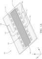
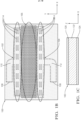
Figures 1a-1c are perspective, top and side views, respectively, of an antenna board utilizing a two-dimensional (2D) electromagnetic band-gap (EBG) structures according to some embodiments. -
Figure 2a is a top view of a 2D EBG structure according to some embodiments,Figure 2b is a top view of a plurality of 2D EBG structure according to some embodiments, andFigure 2c is a cross-sectional view taken along line 2b-2b inFigure 2a . -
Figure 3a is a top view of a 2D EBG structure according to some embodiments,Figure 3b is a top view of a plurality of 2D EBG structure according to some embodiments, andFigure 3c is a cross-sectional view taken along line 3b-3b inFigure 3a . -
Figure 4 is a top view of an antenna board utilizing 2D electromagnetic band-gap (EBG) structures according to some embodiments. -
Figure 5 is a graph illustrating transmission/reception (Tx/Rx) coupling between antennas with and without EBG structures according to some embodiments. - According to one aspect, this disclosure is directed to a two-dimensional electromagnetic band gap structure (EBG) utilized to reduce coupling between adjacent antennas elements. In particular, the EBGs are utilized on an antenna board (e.g., printed circuit boards) that includes at least a planar antenna substrate layer, a top conductive layer and a bottom conductive layer. A number of methods of fabricating antennas may be utilized. For example, in some embodiments antennas elements (i.e., radiating elements) are fabricated on the antenna board via selective etching of the top conductive layer. In other embodiments, rather than selectively etch a top conductive layer to leave a desired conductive pattern, the desired conductive pattern is selectively plated. In other embodiments, various other well-known fabrication techniques may be utilized to fabricate antenna structures, including plastic injection molding. The EBG structures are fabricated in the region between the adjacent antennas and include a repeating or periodic pattern of EBG structures. The EBG structures are likewise fabricated via the selective etching of the top conductive layer. The process of etching the top conductive layer to fabricate the EBG structures is the same as the process of etching the top conductive layer to fabricate the antennas, and thus does not present a substantial additional cost to the fabrication process. In particular, the fabrication process does not require modification of the underlying antenna substrate layer, while still providing the desired decoupling between the adjacent antennas.
- Referring now to
Figures 1a-1c , anantenna board 100 is illustrated that utilizes two-dimensional (2D) electromagnetic band-gap (EBG) structures according to some embodiments. Theantenna board 10 includes at least one receivingantenna 102, at least onetransmission antenna 104, and an EBGregion 105 located between the at least one receivingantenna 102 and the at least onetransmission antenna 104. In some embodiments,antenna board 100 is fabricated on a laminated structure such as a printed circuit board (PCB) having at least a topconductive layer 120, anantenna substrate layer 122, and a bottom conductive layer 124 (shown inFigure 1c ). Radio frequency (RF) waves propagating within theantenna substrate layer 122, constrained in the z-direction by topconductive layer 120 and bottomconductive layer 124. A plurality of conductive vias 111 extending between the topconductive layer 120 and the bottomconductive layer 124 constrain the RF wave in the lateral direction (i.e., in the x-y plane). In this way, RF waveguides are defined within theantenna substrate layer 122 by the topconductive layer 120, bottomconductive layer 124 and plurality of conductive vias 111. RF signals received by the receivingantenna 102 are transmitted viawaveguide 110 tooutput port 106. Likewise, RF signals received atinput port 108 are transmitted viawaveguide 112 totransmission antenna 104. Theantenna board 100 illustrated inFigures 1a and1b is referred to as a slot antenna, wherein the at least one receivingantenna 102 and the at least onetransmission antenna 104 are fabricated by forming a plurality ofslots 114 within the topconductive layer 120. Each slot exposes theantenna substrate layer 122 located adjacent to the topconductive layer 120. Fabrication of theslots 114 may utilize etching (removal) of the topconductive layer 120. In other embodiments, rather than slot antennas, other types of antennas may be fabricated on the PCB such as microstrip antennas, stick antennas, etc. - In some embodiments,
antenna board 100 may be utilized as part of a radar sensing system, in whichtransmission antenna 104 propagates an RF signal and receivingantenna 102 receives a reflection of the RF signal that is utilized to detect, range, and/or track objects. In other embodiments,antenna board 100 may be utilized in a multiple-input multiple output (MIMO) communication system that utilizing a plurality of transmission antennas and a plurality of receiving antennas to provide wireless communication between two points. For example, in the MIMO embodiments, rather than atransmission antenna 104 and areceiving antenna 102 located on the antenna board, butantennas antenna 102 and the at least onetransmission antenna 104 operate in the E-band, which extends from approximately 60 gigahertz (GHz) to 90 GHz. In particular, in some embodiments the at least one receivingantenna 102 and the at least onetransmission antenna 104 operate in a frequency range of between approximately 72 GHz and 82 GHz, and in some embodiments operate in a frequency range of between 76 GHz and 78 GHz. EBGregion 105 is designed to create a stopband within the operating frequency of the at least one receivingantenna 102 and the at least onetransmission antenna 104 to decrease coupling between the respective antennas. In some embodiments, the stopband operates over the E-band range (e.g., 60 GHz-90 GHz). In other embodiments, the EBGregion 105 may be selected to provide a stopband in the frequency of range of between 72 GHz and 82 GHz, and in some embodiments operate in a frequency range of between 76 GHz and 78 GHz. Decreasing the mutual coupling between the respective antennas increases the performance of the respective antennas. For example, in embodiments utilizing the antennas for radar sensing, decreased coupling between therespective transmission antenna 104 and receivingantenna 102 reduces the noise floor associated with each antenna, thereby increasing the signal-to-noise (SNR) ratio of the radar sensing system and increasing the detection range of the radar sensing system. - In some embodiments, the plurality of EBG structures located in the
EBG region 105 are fabricated by selectively etching (removing) conductive material from the topconductive layer 120. One benefit of theantenna board 100 shown inFigures 1a-1c is that the step of etching of the topconductive layer 120 to fabricate theantenna slots 114 for the receiving/transmitting antennas and etching of the topconductive layer 120 to fabricate the plurality of EBG structures may be performed at the same time. That is, the cost of fabricating the plurality of EBG structures withinEBG region 105 is extremely low (approximately zero) as no additional fabrication steps are required. As discussed above, in other embodiments other fabrication methods may be utilized, such as plating techniques and/or injection molding techniques. In general, however, regardless of the fabrication technique utilized, the 2D geometry of the EBG structures - similar to the 2D geometry of the antenna elements in the same plane as the EBG structures - means that fabrication of the antenna elements and fabrication of the EBG structures will not add additional (or much additional) cost to the process. - The geometry of the EBG structures is selected to prevent the propagation of surface waves along the top
conductive layer 120 between the at least one receivingantenna 102 and the at least onetransmission antenna 104. For example, as discussed in more detail with respect toFigure 2 , in some embodiments each EBG structure includes a plurality of slots etched within the top conductive layer that results in a plurality of conductive regions positioned in a defined pattern, separated from one another via the etched slots. In the embodiments shown inFigures 2a-2c , a plurality of square-shaped conductive regions are positioned within an interior of the EBG structure, and a plurality of L-shaped conductive regions are positioned at least partially surrounding each square-shaped conductive region. In another embodiment shown inFigures 3a-3c , the EBG structure is comprised of an H-shaped slot etched in the conductive layer. - Referring to
Figures 2a-2c , anEBG structure 200 according to some embodiments is illustrated.Figure 2a is a top view of asingle EBG structure 200.Figure 2b is a cross-sectional view of theEBG structure 200 taken along line 2b-2b shown inFigure 2a .Figure 2c is a top view illustrating a plurality ofEBG structures 200 according to some embodiments. - In the embodiment shown in
Figure 2a , theEBG structure 200 includes a first plurality ofconductive regions conductive regions underlying antenna substrate 206. As described above, in some embodiments the slots are etched into a planar conductive layer, removing the conductive layer to expose the underlying antenna substrate layer. This is illustrated in the cross-sectional view shown inFigure 2b , in whichconductive regions antenna substrate layer 206. It is also worth pointing out inFigure 2b that theconductive regions conductive regions conductive layer 207. - In the embodiment shown in
Figure 2a , the first plurality ofconductive regions 202a-202d have a geometry defined by lengths L2 and L5. In some embodiments, lengths L2 and L5 are equal to one another, such thatconductive regions 202a-202d are square-shaped. In some embodiments, each of the first plurality ofconductive regions 202a-202d are separated from adjacentconductive regions 202a-202d in the y-direction by a length L6 and in the x-direction by a length L9. In some embodiments, the lengths L6 and L9 are equal to one another, such that each of the first plurality ofconductive regions 202a-202d are located equidistant from one another. - In some embodiments, a second plurality of
conductive regions 204a-204d are located at least partially surrounding the first plurality ofconductive regions 202a-202d. In some embodiments, the second plurality ofconductive regions 204a-204d are L-shaped. For example,conductive region 204d includes a vertical portion 208 (i.e., extending in the y-direction) and a horizontal portion 210 (i.e., extending in the x-direction). The vertical portion 208 is separated from theconductive region 202d by a distance L7 and the horizontal portion 210 is separated from theconductive region 202d by a distance L8. In some embodiments, the distances L7 and L8 are equal to one another. In addition, in some embodiments each of the second plurality ofconductive regions 204a-204d are separated from adjacentconductive regions 204a-204d in the y-direction by a distance L3 and in the x-direction by a distance L4. In some embodiments the distances L3 and L4 are equal to one another. In addition, in some embodiments the distance L9 between firstconductive regions conductive regions conductive regions conductive regions - The dimensions of the
EBG structure 200 is selected based, at least in part, on the desired stopband. For example, in some embodiments the width of the etched slots, expressed in distances L3, L4, L6, L7, L8 and L9 shown inFigure 2 are less than the distances L2 and L5 of the first plurality ofconductive regions conductive regions conductive regions 202a-202d are approximately 0.1 and 0.3 mm and the length of theEBG structure 200 is approximately 0.9 to 1.1 mm. - In the embodiment shown in
Figure 2c , a plurality ofEBG structures conductive regions 204 fromadjacent EBG structures 200a-200d form a single conductive structure having a width defined by distance L10 and L11. In some embodiments, the distances L10 andL1 1 are equal to one another. In some embodiments, the distance L10 and L11 (associated with combined conductive region 204) is approximately the same as distance L2 representing the width ofconductive region 202. In other embodiments, the distance L10, L11is approximately one-half the length of the distance L2, such that the width of the combinedconductive regions 204 are narrower than the width of theconductive regions 202. In other embodiments the width of the combinedconductive regions 204 may be greater than the width of conductive regions 202 (e.g., distance L10, L11 greater than distance L2). - In the embodiment shown in
Figures 1a and1b , a plurality of EBG structures such as EBG structure 200 (shown inFigures 2a-2c ) are utilized in a periodic pattern in the region betweenreceiver antenna 102 andtransmission antenna 104. The number ofEBG structures 200 utilized may vary based on the application. In the embodiment shown inFigures 1a and1b , six total rows ofEBG structures 200 are utilized in theEBG region 105. In other embodiments, additional or fewer rows of EBG structures may be utilized in theEBG region 105. In some embodiments, the periodic inclusion ofEBG structures 200 inEBG region 105 act to reduce surface ripples betweenadjacent antennas adjacent antennas antenna 102 and 104). This reduces the dissimilarity in the antenna radiation pattern and improves the angle-finding accuracy of theantenna board 100. - Referring to
Figures 3a-3c ,EBG structure 300 is illustrated according to some embodiments.Figure 3a is a top view of asingle EBG structure 300.Figure 3b is a cross-sectional view of theEBG structure 300 taken along line 3b-3b, andFigure 3c is a top view of a plurality ofEBG structures 300 fabricated in a periodic or repeating pattern. - With respect to
Figure 3a ,EBG structure 300 includes aconductive region 302 and an H-shapedslot 301 that includes first and secondhorizontal slots vertical slot 306. Thevertical slot 306 connects the first and secondhorizontal slots vertical slot 306 is positioned equidistant from each end of the first and secondhorizontal slots antenna substrate layer 308. This is illustrated in the cross-sectional view shown inFigure 3b , in which H-shapedslot 301 is etched intoconductive layer 302, wherein conductive material is removed to expose the underlyingantenna substrate layer 308. As described with respect toFigure 2b ,conductive regions 302 are not connected to bottomconductive layer 309 by way of conductive vias. - In some embodiments, the width of the first and second
horizontal slot vertical slot 306 is defined by distance L13. In some embodiments, the distance L12 and L13 are approximately equal. The distance between the first and secondhorizontal slots EBG structure 300 is defined by distance L15 and the height of theEBG structure 300 is defined by distance L16. In some embodiments, the distance L15 is greater than the distance L16, such that theEBG structure 300 is rectangular in shape. In some embodiments, the distance L15 is approximately equal to the distance L16, such that theEBG structure 300 is approximately square in shape. In some embodiments, the distance L15 is equal to between 0.9 and 1.1 mm and the distance L16 is equal to between 0.6 and 0.8 mm. In some embodiments, the width of the slots L12 and L13 is between 0.1 and 0.2 mm, and the distance L14 between the first and secondhorizontal slots - In the embodiment shown in
Figure 3c , a plurality of H-shapedEBG structures EBG structures 300a-300d are utilized in the EBG region located between adjacent antennas as shown inFigures 1a and1b . Depending on the application, the number ofEBG structures 300 utilized in a periodic pattern between the adjacent antenna (e.g., receivingantenna 102 andtransmission antenna 104 shown inFigures 1a and1b ) may vary. - Referring to
Figure 4 , a multiple input multiple output (MIMO)antenna board 400 is illustrated that utilizes a plurality ofantenna sticks EBG regions MIMO antenna board 400 may be utilized as a multiple input receiving antenna and/or as a multiple output transmitting antenna.Antenna board 400 includes a plurality of inputs/outputs respective antenna stick Figures 1a and1b in the embodiment utilizing a transmission antenna and a receiving antenna, it is desirable to decrease surface ripples between the plurality of antennas, thereby decoupling the antennas from one another. - In the embodiment shown in
Figure 4 , the plurality ofEBG regions Figures 3a-3c . In the embodiment shown inFigure 4 , each of the plurality ofEBG regions respective antenna sticks Figures 2a-2c may be utilized instead of the H-shaped EBG structures. - In some embodiments, the plurality of
EBG regions adjacent antenna sticks MIMO antenna board 400. - Referring to
Figure 5 , a graph illustrating the transmission/reception (Tx/Rx) coupling between antennas with and without EBG structures within a frequency band of between 74 GHz and 82 GHz according to some embodiments is shown. The data presented inFigure 5 is based on theantenna board 100 shown inFigures 1a and1b , both with and without the presence of anEBG structure 105.Line 500 illustrates the coupling between the transmission antenna and the receiving antenna without the presence of anEBG region 105.Line 502 illustrates coupling between the antennas in the presence ofEBG region 105. The presence of EBG structures reduce coupling between the respective antennas across the monitored frequency band (e.g., 74 GHz-82 GHz). One of the benefits of the disclosed EBG structure is the relatively wide frequency band of the antenna board system. - In this way, the disclosed invention provides a 2D EBG structure for reducing coupling between adjacent antennas fabricated on planar antenna boards, such as slot antennas, stick antennas, and microstrip antennas. The 2D EBG structure is fabricated by etching slots in the top conductive layer in a repeating pattern but does not require modification of the underlying antenna substrate layer. As a result, the EBG structure is defined as 2D because it only requires fabrication (e.g., etching) of the top conductive layer of the planar antenna board. Fabrication of the 2D EBG structure can be performed in conjunction with etching utilized to fabricate the antenna slots and/or antenna sticks, and therefore does not add significantly to the overall cost of antenna board, while providing significant decoupling of antennas within E-band operating frequencies.
- The following are non-exclusive descriptions of possible embodiments of the present invention.
- According to one aspect, an electromagnetic band-gap (EBG) structure includes an antenna substrate layer having a first planar surface and first and second conductive regions fabricated on the first planar surface. The first conductive regions are separated from adjacent first conductive regions by a first distance. The second conductive regions are separated from the first conductive regions by a second distance and at least partially surround the first conductive regions.
- The EBG structure of the preceding paragraph can optionally include, additionally and/or alternatively any, one or more of the following features, configurations and/or additional components.
- For example, the EBG structure may include a bottom conductive layer located opposite of the first planar surface (adjacent to a second planar surface of the antenna substrate), wherein the first conductive regions and the second conductive regions are separated from the bottom conductive layer by the antenna substrate layer.
- The first conductive regions may be separated from one another by slots formed that expose the antenna substrate layer. Likewise, the second conductive regions may be separated from the first conductive regions and from one another by slots formed to expose the antenna substrate layer.
- The second conductive regions may have an 'L'-shaped geometry.
- The first conductive region may have a square geometry.
- The first distance between the first conductive regions (i.e., a first distance) may be approximately equal to the second distance between the first conductive regions and the second conductive regions.
- The second conductive regions may be separated from adjacent second conductive regions by a third distance.
- The third distance may be equal to the first distance and the second distance.
- The first conductive region may be defined by a first width and the second conductive region may be defined by a second width, wherein the second width may be equal to approximately one-half the first width.
- According to another aspect, a planar antenna board includes an antenna substrate layer, a top conductive layer, and a bottom conductive layer. The antenna substrate layer has a first planar surface and a second planar surface opposite the first planar surface. The top conductive layer is located on the first planar surface and the bottom conductive layer is located on the second planar surface. A first E-band antenna is fabricated in the top conductive layer, wherein the first E-band antenna configured to receive/transmit an E-band frequency radio frequency (RF) signal. A second E-band antenna is fabricated in the top conductive layer, the second E-band antenna configured to receive/transmit an E-band frequency RF signal, wherein the second E-band antenna is offset in the x-y plane from the first E-band antenna. A periodic array of two-dimensional electromagnetic band-gap (EBG) structures are also fabricated in the top conductive layer. The periodic array of 2D EBG structures is located between the first E-band antenna and the second E-band antenna, wherein each EBG structure includes a plurality of slots formed in the top conductive layer, wherein the periodic array of 2D EBG structures blocks surface waves in the E-band frequency range.
- The planar antenna board of the preceding paragraph can optionally include, additionally and/or alternatively any, one or more of the following features, configurations and/or additional components.
- For example, each EBG structure may include a conductive region having an H-shaped slot formed within an interior of the conductive region.
- The H-shaped slot may include a first slot, a second slot, and a third slot perpendicular to the first and second slots, wherein the third slot extends between a middle portion of the first and second slots.
- Each EBG structure may include a first conductive regions located on the first planar surface of the antenna substrate and separated from adjacent first conductive regions by a first distance and second conductive regions located on the first planar surface, wherein the second conductive regions are separated from the first conductive regions by a second distance and wherein the second conductive regions at least partially surround the first conductive regions
- The second conductive regions may have an 'L'-shaped geometry.
- The first conductive regions may have a square geometry.
- The first distance may be approximately equal to the second distance.
- The second conductive regions may be separated from adjacent second conductive regions by a third distance.
- The third distance may be equal to the first distance and the second distance.
- The first E-band antenna may be a transmission antenna and the second E-band antenna may be a receiving antenna utilized in a radar sensing system.
- The first E-band antenna and the second E-band antenna may be utilized in a multiple-input multiple-output (MIMO) antenna system.
Claims (15)
- An electromagnetic band-gap (EBG) structure (300) comprising:an antenna substrate layer (308) having a first planar surface and a second planar surface opposite the first planar surface; anda first conductive layer (302) formed on top of the first planar surface of the antenna substrate layer (308), wherein the first conductive layer (302) includes a plurality of H-shaped slots (301) formed within an interior of the first conductive layer (302), each of the H-shaped slots (301) in the first conductive layer (302) exposing the first planar surface of the antenna substrate layer (308),wherein the EBG structure (300) is utilized in a periodic pattern between adjacent antennas (102, 104).
- The EBG structure (300) of claim 1, wherein the EBG structure (300) is utilized in an EBG region (406a, 406b, 406c, 406d) located between adjacent antenna sticks (404a, 404b, 404c).
- The EBG structure (300) of claim 1 or 2, wherein the H-shaped slot (301) includes a first slot (304a), a second slot (304b), and a third slot (306) perpendicular to the first and second slots, wherein the third slot (306) extends between a middle portion of the first slot (304a) and the second slot (304b).
- The EBG structure (300) of claim 3, wherein the first slot (304a) has a first width (L12), the second slot (304b) has a second width, and the third slot (306) has a third width (L13), wherein the first width (L12), the second width and the third width (L13) are equal.
- The EBG structure (300) of claim 3, wherein the first slot (304a) has a first width (L12), the second slot (304b) has a second width, and the third slot (306) has a third width (L13), wherein the first slot (304a) and the second slot (304b) are separated by a first length (L14), wherein the first length (L14) is greater than the first width (L12) and the second width.
- The EBG structure (300) of any one of claims 1 to 5, further including a bottom conductive layer (309) located adjacent to the second planar surface, wherein the first conductive layer (302) is separated from the bottom conductive layer (309) by the antenna substrate layer (308).
- The EBG structure (300) of any one of claims 1 to 6, wherein the EBG structure (300) has a length (L15) and a height (L16), wherein the first slot (304a) and the second slot (304b) extend along at least a portion of the length (L15) and wherein the third slot (306) extends along at least a portion of the height (L16), wherein the length (L15) is greater than the width (L16).
- An electromagnetic band-gap (EBG) structure (200) comprising:an antenna substrate layer (206) having a first planar surface and a second planar surface;first conductive regions (202a, 202b, 202c, 202d) located on the first planar surface of the antenna substrate (206) and separated from adjacent first conductive regions (202a, 202b, 202c, 202d) by a first distance (L6, L9); andsecond conductive regions (204a, 204b, 204c, 204d) located on the first planar surface, wherein the second conductive regions (204a, 204b, 204c, 204d) are separated from the first conductive regions (202a, 202b, 202c, 202d) by a second distance (L7, L8) and wherein the second conductive regions (204a, 204b, 204c, 204d) at least partially surround the first conductive regions (202a, 202b, 202c, 202d),wherein the EBG structure (200) is utilized in a periodic pattern between adjacent antennas (102, 104).
- The EBG structure (200) of claim 8, wherein the EBG structure (200) is utilized in an EBG region (406a, 406b, 406c, 406d) located between adjacent antenna sticks (404a, 404b, 404c).
- The EBG structure (200) of claim 8 or 9, further including a bottom conductive layer (207) located adjacent to the second planar surface, wherein the first conductive regions (202a, 202b, 202c, 202d) and the second conductive regions (204a, 204b, 204c, 204d) are separated from the bottom conductive layer (207) by the antenna substrate layer (206).
- The EBG structure (200) of any one of claims 8 to 10, wherein the first planar surface of the antenna substrate layer (206) is exposed in slots separating the first conductive regions (202a, 202b, 202c, 202d) from one another, slots separating the second conductive regions (204a, 204b, 204c, 204d) from one another, and slots separating the first conductive regions (202a, 202b, 202c, 202d) from the second conductive regions (204a, 204b, 204c, 204d).
- The EBG structure of any one claims 8 to 11, wherein each of the second conductive regions (204a, 204b, 204c, 204d) is 'L'-shaped and each of the first conductive regions (202a, 202b, 202c, 202d) is square.
- The EBG structure of any one of claims 8 to 12, wherein the first distance (L6, L9) is approximately equal to the second distance (L7, L8).
- The EBG structure of any one of claims 8 to 13, wherein the second conductive regions (204a, 204b, 204c, 204d) are separated from adjacent second conductive regions (204a, 204b, 204c, 204d) by a third distance (L3, L4), wherein the third distance (L3, L4) is equal to the first distance (L6, L9) and the second distance (L7, L8).
- The EBG structure of any one of claims 8 to 14, wherein the first conductive region (202a, 202b, 202c, 202d) is defined by a first width (L2, L5) and the second conductive region (204a, 204b, 204c, 204d) is defined by a second width, wherein the second width is approximately one-half the first width.
Applications Claiming Priority (2)
| Application Number | Priority Date | Filing Date | Title |
|---|---|---|---|
| US16/776,799 US11165149B2 (en) | 2020-01-30 | 2020-01-30 | Electromagnetic band gap structure (EBG) |
| EP21151765.1A EP3859874B1 (en) | 2020-01-30 | 2021-01-15 | Electromagnetic band gap structure (ebg) |
Related Parent Applications (2)
| Application Number | Title | Priority Date | Filing Date |
|---|---|---|---|
| EP21151765.1A Division EP3859874B1 (en) | 2020-01-30 | 2021-01-15 | Electromagnetic band gap structure (ebg) |
| EP21151765.1A Division-Into EP3859874B1 (en) | 2020-01-30 | 2021-01-15 | Electromagnetic band gap structure (ebg) |
Publications (1)
| Publication Number | Publication Date |
|---|---|
| EP4287395A1 true EP4287395A1 (en) | 2023-12-06 |
Family
ID=74184570
Family Applications (2)
| Application Number | Title | Priority Date | Filing Date |
|---|---|---|---|
| EP21151765.1A Active EP3859874B1 (en) | 2020-01-30 | 2021-01-15 | Electromagnetic band gap structure (ebg) |
| EP23189713.3A Pending EP4287395A1 (en) | 2020-01-30 | 2021-01-15 | Electromagnetic band gap structure (ebg) |
Family Applications Before (1)
| Application Number | Title | Priority Date | Filing Date |
|---|---|---|---|
| EP21151765.1A Active EP3859874B1 (en) | 2020-01-30 | 2021-01-15 | Electromagnetic band gap structure (ebg) |
Country Status (3)
| Country | Link |
|---|---|
| US (2) | US11165149B2 (en) |
| EP (2) | EP3859874B1 (en) |
| CN (1) | CN113270715A (en) |
Families Citing this family (20)
| Publication number | Priority date | Publication date | Assignee | Title |
|---|---|---|---|---|
| US10944184B2 (en) * | 2019-03-06 | 2021-03-09 | Aptiv Technologies Limited | Slot array antenna including parasitic features |
| US11165149B2 (en) * | 2020-01-30 | 2021-11-02 | Aptiv Technologies Limited | Electromagnetic band gap structure (EBG) |
| TWI738343B (en) * | 2020-05-18 | 2021-09-01 | 為昇科科技股份有限公司 | Meander antenna structure |
| US11681015B2 (en) | 2020-12-18 | 2023-06-20 | Aptiv Technologies Limited | Waveguide with squint alteration |
| US11749883B2 (en) | 2020-12-18 | 2023-09-05 | Aptiv Technologies Limited | Waveguide with radiation slots and parasitic elements for asymmetrical coverage |
| US11901601B2 (en) | 2020-12-18 | 2024-02-13 | Aptiv Technologies Limited | Waveguide with a zigzag for suppressing grating lobes |
| TWI752780B (en) * | 2020-12-31 | 2022-01-11 | 啓碁科技股份有限公司 | Antenna structure with wide beamwidth |
| US12058804B2 (en) | 2021-02-09 | 2024-08-06 | Aptiv Technologies AG | Formed waveguide antennas of a radar assembly |
| US11962085B2 (en) | 2021-05-13 | 2024-04-16 | Aptiv Technologies AG | Two-part folded waveguide having a sinusoidal shape channel including horn shape radiating slots formed therein which are spaced apart by one-half wavelength |
| US11616282B2 (en) | 2021-08-03 | 2023-03-28 | Aptiv Technologies Limited | Transition between a single-ended port and differential ports having stubs that match with input impedances of the single-ended and differential ports |
| CN116130933B (en) * | 2021-11-15 | 2026-05-05 | 英业达科技有限公司 | Antenna device |
| TWI801000B (en) * | 2021-11-22 | 2023-05-01 | 英業達股份有限公司 | Antenna device |
| US12580318B2 (en) * | 2022-02-04 | 2026-03-17 | Sony Group Corporation | Antenna device, radar device, and transfer device |
| US12456816B2 (en) | 2022-05-02 | 2025-10-28 | Aptiv Technologies AG | Waveguide with slot antennas and reflectors |
| US12414228B2 (en) * | 2022-12-07 | 2025-09-09 | Nxp B.V. | Printed circuit board with electromagnetic bandgap structure for launcher in package devices |
| US12489199B2 (en) * | 2022-12-21 | 2025-12-02 | Outdoor Wireless Networks LLC | Base station antennas having partially reflective surface isolation walls |
| US12537308B2 (en) | 2023-01-24 | 2026-01-27 | Aptiv Technologies AG | Symmetrical two-piece waveguide |
| US12148992B2 (en) | 2023-01-25 | 2024-11-19 | Aptiv Technologies AG | Hybrid horn waveguide antenna |
| CN117878593A (en) * | 2023-02-22 | 2024-04-12 | 深圳安智杰科技有限公司 | A two-dimensional EBG structure and planar antenna for improving antenna isolation |
| US12627020B2 (en) | 2023-05-18 | 2026-05-12 | Aptiv Technologies AG | Waveguide with a curved-wall low-pass filter |
Citations (2)
| Publication number | Priority date | Publication date | Assignee | Title |
|---|---|---|---|---|
| CN102510658A (en) * | 2011-09-26 | 2012-06-20 | 北京邮电大学 | Implementation method of H-type groove fractal UC-EBG (Uniplanar Compact Electromagnetic Band Gap) structure oriented to multifrequency antenna substrate |
| WO2018199753A1 (en) * | 2017-04-25 | 2018-11-01 | The Antenna Company International N.V. | Ebg structure, ebg component, and antenna device |
Family Cites Families (43)
| Publication number | Priority date | Publication date | Assignee | Title |
|---|---|---|---|---|
| US6933812B2 (en) | 2002-10-10 | 2005-08-23 | The Regents Of The University Of Michigan | Electro-ferromagnetic, tunable electromagnetic band-gap, and bi-anisotropic composite media using wire configurations |
| US7307596B1 (en) | 2004-07-15 | 2007-12-11 | Rockwell Collins, Inc. | Low-cost one-dimensional electromagnetic band gap waveguide phase shifter based ESA horn antenna |
| GB0616391D0 (en) | 2006-08-18 | 2006-09-27 | Bae Systems Plc | Electromagnetic band-gap structure |
| US7864117B2 (en) * | 2008-05-07 | 2011-01-04 | Nokia Siemens Networks Oy | Wideband or multiband various polarized antenna |
| KR101176800B1 (en) | 2008-12-23 | 2012-08-27 | 한국전자통신연구원 | Arrangement Structure of Electromagnetic Bandgap for Suppressing the Noise and Improving the Signal Integrity |
| FR2944153B1 (en) * | 2009-04-02 | 2013-04-19 | Univ Rennes | PILLBOX TYPE PARALLEL PLATE MULTILAYER ANTENNA AND CORRESPONDING ANTENNA SYSTEM |
| JPWO2012093603A1 (en) * | 2011-01-04 | 2014-06-09 | 日本電気株式会社 | Electromagnetic wave propagation sheet |
| US8648676B2 (en) * | 2011-05-06 | 2014-02-11 | The Royal Institution For The Advancement Of Learning/Mcgill University | Tunable substrate integrated waveguide components |
| US9407011B2 (en) | 2012-02-22 | 2016-08-02 | The United States Of America As Represented By The Secretary Of The Army | Broadband electromagnetic band-gap (EBG) structure |
| FR2985096B1 (en) | 2011-12-21 | 2014-01-24 | Centre Nat Rech Scient | ELEMENTARY ANTENNA AND CORRESPONDING TWO-DIMENSIONAL NETWORK ANTENNA |
| EP2626952B1 (en) | 2012-02-10 | 2014-01-22 | Honeywell International, Inc. | Antenna with effective and electromagnetic bandgap (EBG) media and related system and method |
| CN102683826B (en) | 2012-05-22 | 2014-04-30 | 北京航空航天大学 | ]-E-shaped dual-frequency patch antenna with dual-stop band electromagnetic band-gap structure |
| CN102820501A (en) | 2012-07-03 | 2012-12-12 | 北京邮电大学 | Ultra wideband antenna-oriented crossed H-shaped slot fractal UC-EBG (Uniplanar Compact Electromagnetic bandgap) structure and design method thereof |
| US9515387B2 (en) | 2012-08-17 | 2016-12-06 | Mediatek Inc. | Multi-input multi-output antenna with electromagnetic band-gap structure |
| CN103035460A (en) | 2012-12-31 | 2013-04-10 | 东南大学 | Slow wave structure of coplanar electromagnetic band-gap meander line microwave |
| US9806431B1 (en) * | 2013-04-02 | 2017-10-31 | Waymo Llc | Slotted waveguide array antenna using printed waveguide transmission lines |
| CN103687280B (en) | 2013-12-04 | 2017-07-25 | 西安电子科技大学 | A kind of electromagnetic bandgap structure |
| JP6278720B2 (en) | 2014-01-28 | 2018-02-14 | キヤノン株式会社 | Cell and electromagnetic band gap structure |
| CN103943969A (en) | 2014-05-13 | 2014-07-23 | 北京邮电大学 | Bidirectional symmetrical I-shaped slot uniplanar-compact electromagnetic band-gap structure in millimeter wave antenna |
| CN104332677A (en) | 2014-10-24 | 2015-02-04 | 上海交通大学 | Ultra-wideband plane electromagnetic band-gap structure for suppressing high-speed circuit ground bounce noise |
| US9865935B2 (en) * | 2015-01-12 | 2018-01-09 | Huawei Technologies Co., Ltd. | Printed circuit board for antenna system |
| JP6512402B2 (en) * | 2015-05-20 | 2019-05-15 | パナソニックIpマネジメント株式会社 | Antenna device, wireless communication device, and radar device |
| CN206610893U (en) * | 2015-11-05 | 2017-11-03 | 日本电产艾莱希斯株式会社 | Slot antenna |
| CN105356042B (en) * | 2015-11-23 | 2018-03-06 | 西安电子科技大学 | Small capacity double trap UWB antenna |
| WO2017131099A1 (en) * | 2016-01-29 | 2017-08-03 | Nidec Elesys Corporation | Waveguide device, and antenna device including the waveguide device |
| US10658761B2 (en) * | 2016-03-16 | 2020-05-19 | Huber+Suhner Ag | Adapter structure with waveguide channels |
| US10490907B2 (en) * | 2016-09-27 | 2019-11-26 | Google Llc | Suppression of surface waves in printed circuit board-based phased-array antennas |
| US10283871B2 (en) * | 2016-10-12 | 2019-05-07 | University Of Central Florida Research Foundation, Inc. | Reconfigurable antenna array and associated method of use |
| US10044087B2 (en) * | 2016-10-14 | 2018-08-07 | Microelectronics Technology, Inc. | Switchable radiators and operating method for the same |
| JP2018164149A (en) * | 2017-03-24 | 2018-10-18 | パナソニック株式会社 | Antenna device |
| US10985455B2 (en) * | 2017-04-25 | 2021-04-20 | The Antenna Company International N.V. | EBG structure, EBG component, and antenna device |
| WO2018235593A1 (en) * | 2017-06-23 | 2018-12-27 | 株式会社ソシオネクスト | Antenna device |
| JP2020532891A (en) * | 2017-07-25 | 2020-11-12 | ギャップウェーブス アーベー | Transition device, transition structure, and integrated package structure |
| JP7294608B2 (en) * | 2017-08-18 | 2023-06-20 | ニデックエレシス株式会社 | antenna array |
| DE102018124924A1 (en) * | 2017-10-10 | 2019-04-11 | Nidec Corporation | Waveguiding device |
| CN109041413A (en) | 2018-10-31 | 2018-12-18 | 中国工程物理研究院电子工程研究所 | A kind of depth inhibits the electromagnetic bandgap structure of ultra wide band simultaneous switching noise |
| RU2696676C1 (en) * | 2018-12-06 | 2019-08-05 | Самсунг Электроникс Ко., Лтд. | Ridge waveguide without side walls on base of printed-circuit board and containing its multilayer antenna array |
| JP2020108147A (en) * | 2018-12-27 | 2020-07-09 | 日本電産株式会社 | Antenna device, radar system and communication system |
| CN111446530A (en) * | 2019-01-16 | 2020-07-24 | 日本电产株式会社 | Waveguide device, electromagnetic wave locking device, antenna device, and radar device |
| US10944184B2 (en) * | 2019-03-06 | 2021-03-09 | Aptiv Technologies Limited | Slot array antenna including parasitic features |
| KR102639417B1 (en) * | 2019-05-10 | 2024-02-23 | 삼성전자주식회사 | Electronic device including antenna |
| US11165149B2 (en) * | 2020-01-30 | 2021-11-02 | Aptiv Technologies Limited | Electromagnetic band gap structure (EBG) |
| US11723199B2 (en) * | 2021-03-03 | 2023-08-08 | Taiwan Semiconductor Manufacturing Company, Ltd. | Protective liner layers in 3D memory structure |
-
2020
- 2020-01-30 US US16/776,799 patent/US11165149B2/en active Active
-
2021
- 2021-01-15 EP EP21151765.1A patent/EP3859874B1/en active Active
- 2021-01-15 EP EP23189713.3A patent/EP4287395A1/en active Pending
- 2021-01-29 CN CN202110127142.4A patent/CN113270715A/en active Pending
- 2021-09-29 US US17/488,560 patent/US12009591B2/en active Active
Patent Citations (2)
| Publication number | Priority date | Publication date | Assignee | Title |
|---|---|---|---|---|
| CN102510658A (en) * | 2011-09-26 | 2012-06-20 | 北京邮电大学 | Implementation method of H-type groove fractal UC-EBG (Uniplanar Compact Electromagnetic Band Gap) structure oriented to multifrequency antenna substrate |
| WO2018199753A1 (en) * | 2017-04-25 | 2018-11-01 | The Antenna Company International N.V. | Ebg structure, ebg component, and antenna device |
Non-Patent Citations (4)
| Title |
|---|
| BAIT-SUWAILAM MOHAMMED M: "Isolation Enhancement Between Two Slot Antenna Elements Using Complementary Split-Ring Resonators", INTERNATIONAL JOURNAL OF ENGINEERING RESEARCH AND TECHNOLOGY, vol. 12, no. 9, 30 September 2019 (2019-09-30) - 30 September 2019 (2019-09-30), pages 1561 - 1566, XP093337098, ISSN: 0974-3154, Retrieved from the Internet <URL:https://www.ripublication.com/irph/ijert19/ijertv12n9_27.pdf> [retrieved on 20251118] * |
| KURAVATTI PRAKASH ET AL: "Reduction of mutual coupling in antenna arrays using periodic structures", 2016 IEEE INTERNATIONAL CONFERENCE ON RECENT TRENDS IN ELECTRONICS, INFORMATION & COMMUNICATION TECHNOLOGY (RTEICT), IEEE, 20 May 2016 (2016-05-20), pages 14 - 16, XP033037861, [retrieved on 20170105], DOI: 10.1109/RTEICT.2016.7807772 * |
| STYLIANOS D ASSIMONIS ET AL: "Design and Optimization of Uniplanar EBG Structures for Low Profile Antenna Applications and Mutual Coupling Reduction", IEEE TRANSACTIONS ON ANTENNAS AND PROPAGATION, IEEE SERVICE CENTER, PISCATAWAY, NJ, US, vol. 60, no. 10, 1 October 2012 (2012-10-01), pages 4944 - 4949, XP011466636, ISSN: 0018-926X, DOI: 10.1109/TAP.2012.2210178 * |
| YANG XU ET AL: "Isolation Enhancement in Patch Antenna Array With Fractal UC-EBG Structure and Cross Slot", IEEE ANTENNAS AND WIRELESS PROPAGATION LETTERS, vol. 16, 31 July 2017 (2017-07-31) - 31 July 2017 (2017-07-31), pages 2175 - 2178, XP011657947, ISSN: 1536-1225, [retrieved on 20170731], DOI: 10.1109/LAWP.2017.2703170 * |
Also Published As
| Publication number | Publication date |
|---|---|
| US11165149B2 (en) | 2021-11-02 |
| US20210242581A1 (en) | 2021-08-05 |
| US12009591B2 (en) | 2024-06-11 |
| EP3859874A1 (en) | 2021-08-04 |
| EP3859874B1 (en) | 2023-09-13 |
| US20220021109A1 (en) | 2022-01-20 |
| CN113270715A (en) | 2021-08-17 |
Similar Documents
| Publication | Publication Date | Title |
|---|---|---|
| EP3859874B1 (en) | Electromagnetic band gap structure (ebg) | |
| US6954177B2 (en) | Microstrip antenna array with periodic filters for enhanced performance | |
| KR101621480B1 (en) | Transit structure of waveguide and dielectric waveguide | |
| EP3358676A1 (en) | Module, wireless communication apparatus, and radar apparatus | |
| KR102599824B1 (en) | antenna array | |
| EP4235955B1 (en) | Horn antenna | |
| EP0161044A1 (en) | Dual-frequency microwave antenna | |
| JP2016220029A (en) | Antenna device, radio communication device and radar device | |
| CN109346834A (en) | SIGW circularly polarized slot antenna | |
| CN109950693B (en) | Integrated substrate gap waveguide circularly polarized slot traveling wave array antenna | |
| CN111262025A (en) | Integrated Substrate Gap Waveguide Beam Scanning Leaky Wave Antenna | |
| CN201383549Y (en) | Multi-beam antenna with high radiation efficiency | |
| CN109860990B (en) | Broadband dual-polarized antenna based on integrated substrate gap waveguide | |
| EP3252869B1 (en) | Dielectric substrate and antenna device | |
| CN113659325B (en) | Integrated substrate gap waveguide array antenna | |
| US8378759B2 (en) | First and second coplanar microstrip lines separated by rows of vias for reducing cross-talk there between | |
| CN114583427B (en) | High-frequency signal transmission device and antenna system | |
| CN112666524B (en) | Radar and movable platform | |
| CN113471706A (en) | Low sidelobe antenna array with parasitic radiation suppression function | |
| CN109950688B (en) | Microstrip ISGW circularly polarized slot traveling wave antenna | |
| CN209880807U (en) | SIGW circular polarized antenna | |
| CN222601366U (en) | Millimeter wave radar antenna and radar apparatus | |
| CN114784467A (en) | Signal cross-layer transmission device and antenna system | |
| CN109950694B (en) | Ridged ISGW circularly polarized slot traveling wave antenna | |
| CN216253330U (en) | Receiving and transmitting shielding structure between waveguide and circuit board |
Legal Events
| Date | Code | Title | Description |
|---|---|---|---|
| PUAI | Public reference made under article 153(3) epc to a published international application that has entered the european phase |
Free format text: ORIGINAL CODE: 0009012 |
|
| STAA | Information on the status of an ep patent application or granted ep patent |
Free format text: STATUS: THE APPLICATION HAS BEEN PUBLISHED |
|
| AC | Divisional application: reference to earlier application |
Ref document number: 3859874 Country of ref document: EP Kind code of ref document: P |
|
| AK | Designated contracting states |
Kind code of ref document: A1 Designated state(s): AL AT BE BG CH CY CZ DE DK EE ES FI FR GB GR HR HU IE IS IT LI LT LU LV MC MK MT NL NO PL PT RO RS SE SI SK SM TR |
|
| RAP1 | Party data changed (applicant data changed or rights of an application transferred) |
Owner name: APTIV TECHNOLOGIES AG |
|
| STAA | Information on the status of an ep patent application or granted ep patent |
Free format text: STATUS: REQUEST FOR EXAMINATION WAS MADE |
|
| 17P | Request for examination filed |
Effective date: 20240606 |
|
| RBV | Designated contracting states (corrected) |
Designated state(s): AL AT BE BG CH CY CZ DE DK EE ES FI FR GB GR HR HU IE IS IT LI LT LU LV MC MK MT NL NO PL PT RO RS SE SI SK SM TR |
|
| RAP3 | Party data changed (applicant data changed or rights of an application transferred) |
Owner name: APTIV TECHNOLOGIES AG |
|
| STAA | Information on the status of an ep patent application or granted ep patent |
Free format text: STATUS: EXAMINATION IS IN PROGRESS |
|
| 17Q | First examination report despatched |
Effective date: 20251125 |