EP4287263A1 - Lateral bipolar transistor - Google Patents
Lateral bipolar transistor Download PDFInfo
- Publication number
- EP4287263A1 EP4287263A1 EP23173823.8A EP23173823A EP4287263A1 EP 4287263 A1 EP4287263 A1 EP 4287263A1 EP 23173823 A EP23173823 A EP 23173823A EP 4287263 A1 EP4287263 A1 EP 4287263A1
- Authority
- EP
- European Patent Office
- Prior art keywords
- region
- transistor
- substrate
- collector
- base
- Prior art date
- Legal status (The legal status is an assumption and is not a legal conclusion. Google has not performed a legal analysis and makes no representation as to the accuracy of the status listed.)
- Pending
Links
- 239000000758 substrate Substances 0.000 claims abstract description 110
- XUIMIQQOPSSXEZ-UHFFFAOYSA-N Silicon Chemical compound [Si] XUIMIQQOPSSXEZ-UHFFFAOYSA-N 0.000 claims abstract description 53
- 239000010703 silicon Substances 0.000 claims abstract description 44
- 229910052710 silicon Inorganic materials 0.000 claims abstract description 42
- 239000012212 insulator Substances 0.000 claims abstract description 32
- 238000000034 method Methods 0.000 claims description 31
- 230000010287 polarization Effects 0.000 claims description 30
- FVBUAEGBCNSCDD-UHFFFAOYSA-N silicide(4-) Chemical compound [Si-4] FVBUAEGBCNSCDD-UHFFFAOYSA-N 0.000 claims description 17
- 230000015572 biosynthetic process Effects 0.000 claims description 16
- 239000004065 semiconductor Substances 0.000 claims description 16
- 229910021332 silicide Inorganic materials 0.000 claims description 16
- 230000015556 catabolic process Effects 0.000 claims description 13
- 230000008569 process Effects 0.000 claims description 13
- 238000004519 manufacturing process Methods 0.000 claims description 7
- 238000009413 insulation Methods 0.000 claims description 5
- 230000003247 decreasing effect Effects 0.000 claims description 4
- 229910000927 Ge alloy Inorganic materials 0.000 claims description 2
- 229910000676 Si alloy Inorganic materials 0.000 claims description 2
- 229910000577 Silicon-germanium Inorganic materials 0.000 description 13
- 125000006850 spacer group Chemical group 0.000 description 12
- 230000000694 effects Effects 0.000 description 8
- 229910004298 SiO 2 Inorganic materials 0.000 description 7
- 238000005516 engineering process Methods 0.000 description 6
- VYPSYNLAJGMNEJ-UHFFFAOYSA-N Silicium dioxide Chemical compound O=[Si]=O VYPSYNLAJGMNEJ-UHFFFAOYSA-N 0.000 description 5
- 230000008878 coupling Effects 0.000 description 5
- 238000010168 coupling process Methods 0.000 description 5
- 238000005859 coupling reaction Methods 0.000 description 5
- 230000010355 oscillation Effects 0.000 description 5
- 230000007704 transition Effects 0.000 description 5
- 238000000407 epitaxy Methods 0.000 description 4
- 229910052732 germanium Inorganic materials 0.000 description 4
- GNPVGFCGXDBREM-UHFFFAOYSA-N germanium atom Chemical compound [Ge] GNPVGFCGXDBREM-UHFFFAOYSA-N 0.000 description 4
- 229910021420 polycrystalline silicon Inorganic materials 0.000 description 4
- 229910045601 alloy Inorganic materials 0.000 description 3
- 239000000956 alloy Substances 0.000 description 3
- 238000000151 deposition Methods 0.000 description 3
- 239000003989 dielectric material Substances 0.000 description 3
- 238000005530 etching Methods 0.000 description 3
- 229920005591 polysilicon Polymers 0.000 description 3
- OAICVXFJPJFONN-UHFFFAOYSA-N Phosphorus Chemical compound [P] OAICVXFJPJFONN-UHFFFAOYSA-N 0.000 description 2
- BOTDANWDWHJENH-UHFFFAOYSA-N Tetraethyl orthosilicate Chemical compound CCO[Si](OCC)(OCC)OCC BOTDANWDWHJENH-UHFFFAOYSA-N 0.000 description 2
- 238000004458 analytical method Methods 0.000 description 2
- 229910052785 arsenic Inorganic materials 0.000 description 2
- RQNWIZPPADIBDY-UHFFFAOYSA-N arsenic atom Chemical compound [As] RQNWIZPPADIBDY-UHFFFAOYSA-N 0.000 description 2
- 230000000295 complement effect Effects 0.000 description 2
- 230000008021 deposition Effects 0.000 description 2
- 230000005669 field effect Effects 0.000 description 2
- 239000011810 insulating material Substances 0.000 description 2
- 238000005468 ion implantation Methods 0.000 description 2
- 229910021421 monocrystalline silicon Inorganic materials 0.000 description 2
- 229910052698 phosphorus Inorganic materials 0.000 description 2
- 239000011574 phosphorus Substances 0.000 description 2
- 230000009467 reduction Effects 0.000 description 2
- 230000001846 repelling effect Effects 0.000 description 2
- 235000012239 silicon dioxide Nutrition 0.000 description 2
- 239000000377 silicon dioxide Substances 0.000 description 2
- ZOXJGFHDIHLPTG-UHFFFAOYSA-N Boron Chemical compound [B] ZOXJGFHDIHLPTG-UHFFFAOYSA-N 0.000 description 1
- LEVVHYCKPQWKOP-UHFFFAOYSA-N [Si].[Ge] Chemical compound [Si].[Ge] LEVVHYCKPQWKOP-UHFFFAOYSA-N 0.000 description 1
- 238000009825 accumulation Methods 0.000 description 1
- 229910052796 boron Inorganic materials 0.000 description 1
- 238000004891 communication Methods 0.000 description 1
- 238000009833 condensation Methods 0.000 description 1
- 230000005494 condensation Effects 0.000 description 1
- 239000004020 conductor Substances 0.000 description 1
- 230000005684 electric field Effects 0.000 description 1
- 230000014509 gene expression Effects 0.000 description 1
- 238000003384 imaging method Methods 0.000 description 1
- 238000002347 injection Methods 0.000 description 1
- 239000007924 injection Substances 0.000 description 1
- 230000010354 integration Effects 0.000 description 1
- 238000001459 lithography Methods 0.000 description 1
- 239000000463 material Substances 0.000 description 1
- 229910052751 metal Inorganic materials 0.000 description 1
- 239000002184 metal Substances 0.000 description 1
- 229910044991 metal oxide Inorganic materials 0.000 description 1
- 150000004706 metal oxides Chemical class 0.000 description 1
- 230000007935 neutral effect Effects 0.000 description 1
- 239000013307 optical fiber Substances 0.000 description 1
- 230000003647 oxidation Effects 0.000 description 1
- 238000007254 oxidation reaction Methods 0.000 description 1
- 238000000206 photolithography Methods 0.000 description 1
- 229910052814 silicon oxide Inorganic materials 0.000 description 1
- 239000000126 substance Substances 0.000 description 1
Images


Classifications
-
- H—ELECTRICITY
- H01—ELECTRIC ELEMENTS
- H01L—SEMICONDUCTOR DEVICES NOT COVERED BY CLASS H10
- H01L29/00—Semiconductor devices specially adapted for rectifying, amplifying, oscillating or switching and having potential barriers; Capacitors or resistors having potential barriers, e.g. a PN-junction depletion layer or carrier concentration layer; Details of semiconductor bodies or of electrodes thereof ; Multistep manufacturing processes therefor
- H01L29/66—Types of semiconductor device ; Multistep manufacturing processes therefor
- H01L29/68—Types of semiconductor device ; Multistep manufacturing processes therefor controllable by only the electric current supplied, or only the electric potential applied, to an electrode which does not carry the current to be rectified, amplified or switched
- H01L29/70—Bipolar devices
- H01L29/72—Transistor-type devices, i.e. able to continuously respond to applied control signals
- H01L29/73—Bipolar junction transistors
- H01L29/735—Lateral transistors
-
- H—ELECTRICITY
- H01—ELECTRIC ELEMENTS
- H01L—SEMICONDUCTOR DEVICES NOT COVERED BY CLASS H10
- H01L29/00—Semiconductor devices specially adapted for rectifying, amplifying, oscillating or switching and having potential barriers; Capacitors or resistors having potential barriers, e.g. a PN-junction depletion layer or carrier concentration layer; Details of semiconductor bodies or of electrodes thereof ; Multistep manufacturing processes therefor
- H01L29/02—Semiconductor bodies ; Multistep manufacturing processes therefor
- H01L29/06—Semiconductor bodies ; Multistep manufacturing processes therefor characterised by their shape; characterised by the shapes, relative sizes, or dispositions of the semiconductor regions ; characterised by the concentration or distribution of impurities within semiconductor regions
- H01L29/10—Semiconductor bodies ; Multistep manufacturing processes therefor characterised by their shape; characterised by the shapes, relative sizes, or dispositions of the semiconductor regions ; characterised by the concentration or distribution of impurities within semiconductor regions with semiconductor regions connected to an electrode not carrying current to be rectified, amplified or switched and such electrode being part of a semiconductor device which comprises three or more electrodes
- H01L29/1004—Base region of bipolar transistors
- H01L29/1008—Base region of bipolar transistors of lateral transistors
-
- H—ELECTRICITY
- H01—ELECTRIC ELEMENTS
- H01L—SEMICONDUCTOR DEVICES NOT COVERED BY CLASS H10
- H01L25/00—Assemblies consisting of a plurality of individual semiconductor or other solid state devices ; Multistep manufacturing processes thereof
- H01L25/03—Assemblies consisting of a plurality of individual semiconductor or other solid state devices ; Multistep manufacturing processes thereof all the devices being of a type provided for in the same subgroup of groups H01L27/00 - H01L33/00, or in a single subclass of H10K, H10N, e.g. assemblies of rectifier diodes
- H01L25/04—Assemblies consisting of a plurality of individual semiconductor or other solid state devices ; Multistep manufacturing processes thereof all the devices being of a type provided for in the same subgroup of groups H01L27/00 - H01L33/00, or in a single subclass of H10K, H10N, e.g. assemblies of rectifier diodes the devices not having separate containers
- H01L25/07—Assemblies consisting of a plurality of individual semiconductor or other solid state devices ; Multistep manufacturing processes thereof all the devices being of a type provided for in the same subgroup of groups H01L27/00 - H01L33/00, or in a single subclass of H10K, H10N, e.g. assemblies of rectifier diodes the devices not having separate containers the devices being of a type provided for in group H01L29/00
- H01L25/072—Assemblies consisting of a plurality of individual semiconductor or other solid state devices ; Multistep manufacturing processes thereof all the devices being of a type provided for in the same subgroup of groups H01L27/00 - H01L33/00, or in a single subclass of H10K, H10N, e.g. assemblies of rectifier diodes the devices not having separate containers the devices being of a type provided for in group H01L29/00 the devices being arranged next to each other
-
- H—ELECTRICITY
- H01—ELECTRIC ELEMENTS
- H01L—SEMICONDUCTOR DEVICES NOT COVERED BY CLASS H10
- H01L27/00—Devices consisting of a plurality of semiconductor or other solid-state components formed in or on a common substrate
- H01L27/02—Devices consisting of a plurality of semiconductor or other solid-state components formed in or on a common substrate including semiconductor components specially adapted for rectifying, oscillating, amplifying or switching and having potential barriers; including integrated passive circuit elements having potential barriers
- H01L27/04—Devices consisting of a plurality of semiconductor or other solid-state components formed in or on a common substrate including semiconductor components specially adapted for rectifying, oscillating, amplifying or switching and having potential barriers; including integrated passive circuit elements having potential barriers the substrate being a semiconductor body
- H01L27/08—Devices consisting of a plurality of semiconductor or other solid-state components formed in or on a common substrate including semiconductor components specially adapted for rectifying, oscillating, amplifying or switching and having potential barriers; including integrated passive circuit elements having potential barriers the substrate being a semiconductor body including only semiconductor components of a single kind
- H01L27/082—Devices consisting of a plurality of semiconductor or other solid-state components formed in or on a common substrate including semiconductor components specially adapted for rectifying, oscillating, amplifying or switching and having potential barriers; including integrated passive circuit elements having potential barriers the substrate being a semiconductor body including only semiconductor components of a single kind including bipolar components only
-
- H—ELECTRICITY
- H01—ELECTRIC ELEMENTS
- H01L—SEMICONDUCTOR DEVICES NOT COVERED BY CLASS H10
- H01L29/00—Semiconductor devices specially adapted for rectifying, amplifying, oscillating or switching and having potential barriers; Capacitors or resistors having potential barriers, e.g. a PN-junction depletion layer or carrier concentration layer; Details of semiconductor bodies or of electrodes thereof ; Multistep manufacturing processes therefor
- H01L29/02—Semiconductor bodies ; Multistep manufacturing processes therefor
- H01L29/06—Semiconductor bodies ; Multistep manufacturing processes therefor characterised by their shape; characterised by the shapes, relative sizes, or dispositions of the semiconductor regions ; characterised by the concentration or distribution of impurities within semiconductor regions
- H01L29/0603—Semiconductor bodies ; Multistep manufacturing processes therefor characterised by their shape; characterised by the shapes, relative sizes, or dispositions of the semiconductor regions ; characterised by the concentration or distribution of impurities within semiconductor regions characterised by particular constructional design considerations, e.g. for preventing surface leakage, for controlling electric field concentration or for internal isolations regions
- H01L29/0607—Semiconductor bodies ; Multistep manufacturing processes therefor characterised by their shape; characterised by the shapes, relative sizes, or dispositions of the semiconductor regions ; characterised by the concentration or distribution of impurities within semiconductor regions characterised by particular constructional design considerations, e.g. for preventing surface leakage, for controlling electric field concentration or for internal isolations regions for preventing surface leakage or controlling electric field concentration
- H01L29/0611—Semiconductor bodies ; Multistep manufacturing processes therefor characterised by their shape; characterised by the shapes, relative sizes, or dispositions of the semiconductor regions ; characterised by the concentration or distribution of impurities within semiconductor regions characterised by particular constructional design considerations, e.g. for preventing surface leakage, for controlling electric field concentration or for internal isolations regions for preventing surface leakage or controlling electric field concentration for increasing or controlling the breakdown voltage of reverse biased devices
-
- H—ELECTRICITY
- H01—ELECTRIC ELEMENTS
- H01L—SEMICONDUCTOR DEVICES NOT COVERED BY CLASS H10
- H01L29/00—Semiconductor devices specially adapted for rectifying, amplifying, oscillating or switching and having potential barriers; Capacitors or resistors having potential barriers, e.g. a PN-junction depletion layer or carrier concentration layer; Details of semiconductor bodies or of electrodes thereof ; Multistep manufacturing processes therefor
- H01L29/02—Semiconductor bodies ; Multistep manufacturing processes therefor
- H01L29/06—Semiconductor bodies ; Multistep manufacturing processes therefor characterised by their shape; characterised by the shapes, relative sizes, or dispositions of the semiconductor regions ; characterised by the concentration or distribution of impurities within semiconductor regions
- H01L29/0684—Semiconductor bodies ; Multistep manufacturing processes therefor characterised by their shape; characterised by the shapes, relative sizes, or dispositions of the semiconductor regions ; characterised by the concentration or distribution of impurities within semiconductor regions characterised by the shape, relative sizes or dispositions of the semiconductor regions or junctions between the regions
-
- H—ELECTRICITY
- H01—ELECTRIC ELEMENTS
- H01L—SEMICONDUCTOR DEVICES NOT COVERED BY CLASS H10
- H01L29/00—Semiconductor devices specially adapted for rectifying, amplifying, oscillating or switching and having potential barriers; Capacitors or resistors having potential barriers, e.g. a PN-junction depletion layer or carrier concentration layer; Details of semiconductor bodies or of electrodes thereof ; Multistep manufacturing processes therefor
- H01L29/02—Semiconductor bodies ; Multistep manufacturing processes therefor
- H01L29/06—Semiconductor bodies ; Multistep manufacturing processes therefor characterised by their shape; characterised by the shapes, relative sizes, or dispositions of the semiconductor regions ; characterised by the concentration or distribution of impurities within semiconductor regions
- H01L29/08—Semiconductor bodies ; Multistep manufacturing processes therefor characterised by their shape; characterised by the shapes, relative sizes, or dispositions of the semiconductor regions ; characterised by the concentration or distribution of impurities within semiconductor regions with semiconductor regions connected to an electrode carrying current to be rectified, amplified or switched and such electrode being part of a semiconductor device which comprises three or more electrodes
- H01L29/0804—Emitter regions of bipolar transistors
- H01L29/0808—Emitter regions of bipolar transistors of lateral transistors
-
- H—ELECTRICITY
- H01—ELECTRIC ELEMENTS
- H01L—SEMICONDUCTOR DEVICES NOT COVERED BY CLASS H10
- H01L29/00—Semiconductor devices specially adapted for rectifying, amplifying, oscillating or switching and having potential barriers; Capacitors or resistors having potential barriers, e.g. a PN-junction depletion layer or carrier concentration layer; Details of semiconductor bodies or of electrodes thereof ; Multistep manufacturing processes therefor
- H01L29/02—Semiconductor bodies ; Multistep manufacturing processes therefor
- H01L29/06—Semiconductor bodies ; Multistep manufacturing processes therefor characterised by their shape; characterised by the shapes, relative sizes, or dispositions of the semiconductor regions ; characterised by the concentration or distribution of impurities within semiconductor regions
- H01L29/08—Semiconductor bodies ; Multistep manufacturing processes therefor characterised by their shape; characterised by the shapes, relative sizes, or dispositions of the semiconductor regions ; characterised by the concentration or distribution of impurities within semiconductor regions with semiconductor regions connected to an electrode carrying current to be rectified, amplified or switched and such electrode being part of a semiconductor device which comprises three or more electrodes
- H01L29/0804—Emitter regions of bipolar transistors
- H01L29/0817—Emitter regions of bipolar transistors of heterojunction bipolar transistors
-
- H—ELECTRICITY
- H01—ELECTRIC ELEMENTS
- H01L—SEMICONDUCTOR DEVICES NOT COVERED BY CLASS H10
- H01L29/00—Semiconductor devices specially adapted for rectifying, amplifying, oscillating or switching and having potential barriers; Capacitors or resistors having potential barriers, e.g. a PN-junction depletion layer or carrier concentration layer; Details of semiconductor bodies or of electrodes thereof ; Multistep manufacturing processes therefor
- H01L29/02—Semiconductor bodies ; Multistep manufacturing processes therefor
- H01L29/06—Semiconductor bodies ; Multistep manufacturing processes therefor characterised by their shape; characterised by the shapes, relative sizes, or dispositions of the semiconductor regions ; characterised by the concentration or distribution of impurities within semiconductor regions
- H01L29/08—Semiconductor bodies ; Multistep manufacturing processes therefor characterised by their shape; characterised by the shapes, relative sizes, or dispositions of the semiconductor regions ; characterised by the concentration or distribution of impurities within semiconductor regions with semiconductor regions connected to an electrode carrying current to be rectified, amplified or switched and such electrode being part of a semiconductor device which comprises three or more electrodes
- H01L29/0821—Collector regions of bipolar transistors
-
- H—ELECTRICITY
- H01—ELECTRIC ELEMENTS
- H01L—SEMICONDUCTOR DEVICES NOT COVERED BY CLASS H10
- H01L29/00—Semiconductor devices specially adapted for rectifying, amplifying, oscillating or switching and having potential barriers; Capacitors or resistors having potential barriers, e.g. a PN-junction depletion layer or carrier concentration layer; Details of semiconductor bodies or of electrodes thereof ; Multistep manufacturing processes therefor
- H01L29/40—Electrodes ; Multistep manufacturing processes therefor
- H01L29/402—Field plates
-
- H—ELECTRICITY
- H01—ELECTRIC ELEMENTS
- H01L—SEMICONDUCTOR DEVICES NOT COVERED BY CLASS H10
- H01L29/00—Semiconductor devices specially adapted for rectifying, amplifying, oscillating or switching and having potential barriers; Capacitors or resistors having potential barriers, e.g. a PN-junction depletion layer or carrier concentration layer; Details of semiconductor bodies or of electrodes thereof ; Multistep manufacturing processes therefor
- H01L29/40—Electrodes ; Multistep manufacturing processes therefor
- H01L29/41—Electrodes ; Multistep manufacturing processes therefor characterised by their shape, relative sizes or dispositions
- H01L29/417—Electrodes ; Multistep manufacturing processes therefor characterised by their shape, relative sizes or dispositions carrying the current to be rectified, amplified or switched
- H01L29/41708—Emitter or collector electrodes for bipolar transistors
-
- H—ELECTRICITY
- H01—ELECTRIC ELEMENTS
- H01L—SEMICONDUCTOR DEVICES NOT COVERED BY CLASS H10
- H01L29/00—Semiconductor devices specially adapted for rectifying, amplifying, oscillating or switching and having potential barriers; Capacitors or resistors having potential barriers, e.g. a PN-junction depletion layer or carrier concentration layer; Details of semiconductor bodies or of electrodes thereof ; Multistep manufacturing processes therefor
- H01L29/40—Electrodes ; Multistep manufacturing processes therefor
- H01L29/41—Electrodes ; Multistep manufacturing processes therefor characterised by their shape, relative sizes or dispositions
- H01L29/423—Electrodes ; Multistep manufacturing processes therefor characterised by their shape, relative sizes or dispositions not carrying the current to be rectified, amplified or switched
- H01L29/42304—Base electrodes for bipolar transistors
-
- H—ELECTRICITY
- H01—ELECTRIC ELEMENTS
- H01L—SEMICONDUCTOR DEVICES NOT COVERED BY CLASS H10
- H01L29/00—Semiconductor devices specially adapted for rectifying, amplifying, oscillating or switching and having potential barriers; Capacitors or resistors having potential barriers, e.g. a PN-junction depletion layer or carrier concentration layer; Details of semiconductor bodies or of electrodes thereof ; Multistep manufacturing processes therefor
- H01L29/66—Types of semiconductor device ; Multistep manufacturing processes therefor
- H01L29/66007—Multistep manufacturing processes
- H01L29/66075—Multistep manufacturing processes of devices having semiconductor bodies comprising group 14 or group 13/15 materials
- H01L29/66227—Multistep manufacturing processes of devices having semiconductor bodies comprising group 14 or group 13/15 materials the devices being controllable only by the electric current supplied or the electric potential applied, to an electrode which does not carry the current to be rectified, amplified or switched, e.g. three-terminal devices
- H01L29/66234—Bipolar junction transistors [BJT]
- H01L29/66242—Heterojunction transistors [HBT]
-
- H—ELECTRICITY
- H01—ELECTRIC ELEMENTS
- H01L—SEMICONDUCTOR DEVICES NOT COVERED BY CLASS H10
- H01L29/00—Semiconductor devices specially adapted for rectifying, amplifying, oscillating or switching and having potential barriers; Capacitors or resistors having potential barriers, e.g. a PN-junction depletion layer or carrier concentration layer; Details of semiconductor bodies or of electrodes thereof ; Multistep manufacturing processes therefor
- H01L29/66—Types of semiconductor device ; Multistep manufacturing processes therefor
- H01L29/66007—Multistep manufacturing processes
- H01L29/66075—Multistep manufacturing processes of devices having semiconductor bodies comprising group 14 or group 13/15 materials
- H01L29/66227—Multistep manufacturing processes of devices having semiconductor bodies comprising group 14 or group 13/15 materials the devices being controllable only by the electric current supplied or the electric potential applied, to an electrode which does not carry the current to be rectified, amplified or switched, e.g. three-terminal devices
- H01L29/66234—Bipolar junction transistors [BJT]
- H01L29/6625—Lateral transistors
-
- H—ELECTRICITY
- H01—ELECTRIC ELEMENTS
- H01L—SEMICONDUCTOR DEVICES NOT COVERED BY CLASS H10
- H01L29/00—Semiconductor devices specially adapted for rectifying, amplifying, oscillating or switching and having potential barriers; Capacitors or resistors having potential barriers, e.g. a PN-junction depletion layer or carrier concentration layer; Details of semiconductor bodies or of electrodes thereof ; Multistep manufacturing processes therefor
- H01L29/66—Types of semiconductor device ; Multistep manufacturing processes therefor
- H01L29/66007—Multistep manufacturing processes
- H01L29/66075—Multistep manufacturing processes of devices having semiconductor bodies comprising group 14 or group 13/15 materials
- H01L29/66227—Multistep manufacturing processes of devices having semiconductor bodies comprising group 14 or group 13/15 materials the devices being controllable only by the electric current supplied or the electric potential applied, to an electrode which does not carry the current to be rectified, amplified or switched, e.g. three-terminal devices
- H01L29/66234—Bipolar junction transistors [BJT]
- H01L29/66272—Silicon vertical transistors
-
- H—ELECTRICITY
- H01—ELECTRIC ELEMENTS
- H01L—SEMICONDUCTOR DEVICES NOT COVERED BY CLASS H10
- H01L29/00—Semiconductor devices specially adapted for rectifying, amplifying, oscillating or switching and having potential barriers; Capacitors or resistors having potential barriers, e.g. a PN-junction depletion layer or carrier concentration layer; Details of semiconductor bodies or of electrodes thereof ; Multistep manufacturing processes therefor
- H01L29/66—Types of semiconductor device ; Multistep manufacturing processes therefor
- H01L29/66007—Multistep manufacturing processes
- H01L29/66075—Multistep manufacturing processes of devices having semiconductor bodies comprising group 14 or group 13/15 materials
- H01L29/66227—Multistep manufacturing processes of devices having semiconductor bodies comprising group 14 or group 13/15 materials the devices being controllable only by the electric current supplied or the electric potential applied, to an electrode which does not carry the current to be rectified, amplified or switched, e.g. three-terminal devices
- H01L29/66234—Bipolar junction transistors [BJT]
- H01L29/6631—Bipolar junction transistors [BJT] with an active layer made of a group 13/15 material
-
- H—ELECTRICITY
- H01—ELECTRIC ELEMENTS
- H01L—SEMICONDUCTOR DEVICES NOT COVERED BY CLASS H10
- H01L29/00—Semiconductor devices specially adapted for rectifying, amplifying, oscillating or switching and having potential barriers; Capacitors or resistors having potential barriers, e.g. a PN-junction depletion layer or carrier concentration layer; Details of semiconductor bodies or of electrodes thereof ; Multistep manufacturing processes therefor
- H01L29/66—Types of semiconductor device ; Multistep manufacturing processes therefor
- H01L29/68—Types of semiconductor device ; Multistep manufacturing processes therefor controllable by only the electric current supplied, or only the electric potential applied, to an electrode which does not carry the current to be rectified, amplified or switched
- H01L29/70—Bipolar devices
- H01L29/72—Transistor-type devices, i.e. able to continuously respond to applied control signals
- H01L29/73—Bipolar junction transistors
- H01L29/7302—Bipolar junction transistors structurally associated with other devices
-
- H—ELECTRICITY
- H01—ELECTRIC ELEMENTS
- H01L—SEMICONDUCTOR DEVICES NOT COVERED BY CLASS H10
- H01L29/00—Semiconductor devices specially adapted for rectifying, amplifying, oscillating or switching and having potential barriers; Capacitors or resistors having potential barriers, e.g. a PN-junction depletion layer or carrier concentration layer; Details of semiconductor bodies or of electrodes thereof ; Multistep manufacturing processes therefor
- H01L29/66—Types of semiconductor device ; Multistep manufacturing processes therefor
- H01L29/68—Types of semiconductor device ; Multistep manufacturing processes therefor controllable by only the electric current supplied, or only the electric potential applied, to an electrode which does not carry the current to be rectified, amplified or switched
- H01L29/70—Bipolar devices
- H01L29/72—Transistor-type devices, i.e. able to continuously respond to applied control signals
- H01L29/73—Bipolar junction transistors
- H01L29/732—Vertical transistors
- H01L29/7322—Vertical transistors having emitter-base and base-collector junctions leaving at the same surface of the body, e.g. planar transistor
-
- H—ELECTRICITY
- H01—ELECTRIC ELEMENTS
- H01L—SEMICONDUCTOR DEVICES NOT COVERED BY CLASS H10
- H01L29/00—Semiconductor devices specially adapted for rectifying, amplifying, oscillating or switching and having potential barriers; Capacitors or resistors having potential barriers, e.g. a PN-junction depletion layer or carrier concentration layer; Details of semiconductor bodies or of electrodes thereof ; Multistep manufacturing processes therefor
- H01L29/66—Types of semiconductor device ; Multistep manufacturing processes therefor
- H01L29/68—Types of semiconductor device ; Multistep manufacturing processes therefor controllable by only the electric current supplied, or only the electric potential applied, to an electrode which does not carry the current to be rectified, amplified or switched
- H01L29/70—Bipolar devices
- H01L29/72—Transistor-type devices, i.e. able to continuously respond to applied control signals
- H01L29/73—Bipolar junction transistors
- H01L29/737—Hetero-junction transistors
-
- H—ELECTRICITY
- H01—ELECTRIC ELEMENTS
- H01L—SEMICONDUCTOR DEVICES NOT COVERED BY CLASS H10
- H01L29/00—Semiconductor devices specially adapted for rectifying, amplifying, oscillating or switching and having potential barriers; Capacitors or resistors having potential barriers, e.g. a PN-junction depletion layer or carrier concentration layer; Details of semiconductor bodies or of electrodes thereof ; Multistep manufacturing processes therefor
- H01L29/02—Semiconductor bodies ; Multistep manufacturing processes therefor
- H01L29/36—Semiconductor bodies ; Multistep manufacturing processes therefor characterised by the concentration or distribution of impurities in the bulk material
Definitions
- This description generally concerns electronic components and more specifically bipolar transistors and their manufacturing process.
- the present description relates in particular to lateral bipolar transistors, and electronic circuits comprising at least one lateral bipolar transistor.
- a bipolar transistor is an electronic component based on a semiconductor from the transistor family. Its operating principle is based on two PN junctions, one forward and the other reverse, the two junctions being formed by a base region between an emitter region and a collector region.
- a lateral bipolar transistor is a bipolar transistor in which the emitter, base, and collector regions are arranged next to each other in, and in some cases on, a semiconductor substrate, unlike a vertical bipolar transistor where these regions are arranged one on top of the other.
- a lateral bipolar transistor is well suited for integration into a Complementary Metal Oxide Semiconductor (CMOS) process, for example due to many structural similarities between a lateral bipolar transistor and an insulated gate field effect transistor (MOSFET, metal- oxide-semiconductor field-effect transistor).
- CMOS Complementary Metal Oxide Semiconductor
- a lateral bipolar transistor for example the increase in its switching speed and/or its breakdown voltage, for which we generally seeks the best compromise for the intended application.
- One embodiment overcomes all or part of the drawbacks of known bipolar transistors, in particular known lateral bipolar transistors.
- the transistor comprises an extrinsic base having a third width and arranged on the base region having a fourth width.
- the third width of the extrinsic base is less than the fourth width of the base region, the extrinsic base being for example substantially centered relative to the base region.
- the transistor comprises a first portion of insulator on a first portion of the emitter region and a second portion of insulator on a first portion of the collector region, the base region being between the first portion of the emitter region and the first portion of the collector region, and the extrinsic base being between the first insulator portion and the second insulator portion.
- the silicon layer has a thickness of between a few nanometers and around fifteen nanometers, for example between 5 and 15 nanometers.
- the insulating layer has a thickness of between a few nanometers and a few tens of nanometers, for example between 10 and 50 nanometers.
- the emitter region is formed by a heavily doped region of the first conductivity type.
- the collector region comprises a first sub-region lightly doped with the first conductivity type and a second sub-region heavily doped with the first conductivity type.
- the first sub-region of the collector region is between the base region and the second sub-region of the collector region.
- the first sub-region of the collector region has an average doping concentration of the first type of conductivity lower than the average doping concentration of the region basic in the second type of conductivity, for example by a factor of at least ten.
- the base region comprises a silicon and germanium alloy.
- the transistor comprises a first insulating trench passing through the silicon layer, the insulating layer and, partially, the semiconductor substrate, said first insulating trench being positioned laterally between the collector region and the substrate region.
- the transistor comprises a second insulating trench passing through the silicon layer, the insulating layer and, partially, the semiconductor substrate, the emitter region being positioned laterally between said second insulating trench and the base region .
- an area of the substrate located at least under the substrate region devoid of the silicon layer and the insulating layer, and preferably under the collector region, is doped, for example with gradual doping decreasing radially from said region of the substrate.
- the transistor includes contacts on the emitter region, the collector region, the substrate region, and, in some cases, on the extrinsic base, the bias circuit being connected to the region of substrate by one of said contact points, a portion of silicide being for example formed under each contact point.
- One embodiment provides a method of using a transistor according to one embodiment, said method comprising applying, by the bias circuit, a bias voltage to the substrate region.
- the method of use comprises applying a positive bias voltage to the substrate region, so as to increase the speed and/or gain of the transistor.
- the method of use comprises applying a negative bias voltage to the substrate region, so as to increase the breakdown voltage of the transistor.
- One embodiment provides an electronic circuit comprising at least one transistor according to one embodiment.
- One embodiment provides an electronic circuit comprising several transistors according to one embodiment, at least two transistors having different bias voltages applied to the substrate region.
- a width or a distance corresponds to a dimension in the lateral direction of a lateral bipolar transistor, which corresponds to the horizontal direction vertical direction Z marked in the figures.
- the expressions “approximately”, “approximately”, “substantially”, and “of the order of” mean to the nearest 10%, preferably to the nearest 5%.
- the embodiments shown in the figures, and described in the description which follows, comprise a lateral bipolar transistor of the NPN type, the N doping corresponding to the first type of conductivity, and the P doping to the second type of conductivity.
- FIG. 1 is a sectional view showing a bipolar transistor 100 according to one embodiment.
- the transistor 100 shown is manufactured in SOI technology and comprises a substrate 102 (SUB), an insulator 104 created in the substrate 102 using, for example, a SIMOX process or a SMARTCUT process, and a thin layer of monocrystalline silicon (Si) 110 on the insulator 104.
- the substrate 102 is based on silicon (Si).
- the insulator 104 can be an oxide (BOX, from English Buried Oxide), for example based on silicon dioxide (SiO 2 ).
- the transistor is in so-called “Fully-Depleted SOI” (FD-SOI) technology, that is to say allowing it to operate in completely depleted mode, with reference to the operation of CMOS FD-SOI transistors.
- FD-SOI Fluly-Depleted SOI
- the thin layer of silicon 110 has a thickness e10 of between a few nanometers and around fifteen nanometers, for example between 5 and 15 nm.
- the insulating layer 104 has a thickness e4 of between a few nanometers and a few tens of nanometers, for example between 10 and 50 nm.
- the transistor 100 includes an N-doped emitter region 112, an N-doped collector region 116, and a P-doped base region 114 formed between the emitter region 112 and the collector region 116.
- the emitter region 112, the base region 114 and the collector region 116 are formed laterally next to each other in the silicon layer 110, the base region being between the emitter region and the collector region.
- the emitter region 112 is heavily N doped (N+), the base region 114 is heavily P doped (P+), and the collector region 116 includes a first lightly N doped collector subregion 116a (N-) and a first collector subregion 116a.
- second collector sub-region 116b heavily doped N (N+), the first collector sub-region 116a being disposed between the base region 114 and the second collector sub-region 116b.
- This doping difference between the emitter and the collector creates a doping asymmetry of the transistor.
- the width L16 of the collector region 116 is greater than the width L12 of the emitter region 112, creating a geometric asymmetry of the transistor.
- transistor 100 is said to be asymmetric geometrically and by doping.
- “heavily doped” means having an average doping concentration greater than or equal to 1.10 19 at/cm 3 and "lightly doped” means having an average doping concentration less than 1.10 19 at/cm 3 .
- the portion of the silicon layer corresponding to the base region 114 can be treated in order to form a silicon-germanium alloy (SiGe) in said base region.
- Germanium in the base helps improve performance of the transistor, which is then of the heterojunction type (HBT, from English Heterojunction Bipolar Transistor).
- HBT heterojunction type
- adding germanium to the base region can reduce the voltage between the emitter region and the base region due to the smaller bandgap of SiGe alloy compared to silicon.
- the base region is made of silicon, the transistor then being a homojunction type transistor (BJT, from English Bipolar Junction Transistor).
- This base region 114 corresponds to a so-called “intrinsic” base region (active part of the base, between the emitter region and the collector region).
- extrinsic base region 118 is surmounted by a so-called “extrinsic” base region 118, which can also be designated by the term “extrinsic base”, and which is an electrical connection part, through which the intrinsic region base 114 can be biased during operation of the transistor.
- the extrinsic base 118 is for example based on polycrystalline silicon, or polysilicon (Poly).
- the width L18 of the extrinsic base 118 is less than the width L14 of the base region 114, and the extrinsic base positioned relative to the base region so that first and second portions 114a, 114b at both ends lateral parts of the base region 114 are not covered by the extrinsic base 118.
- the width L14 of the base region 114 is between approximately 10 and 100 nm
- the width L18 of the extrinsic base 118 is between approximately 5 and 90 nm, the extrinsic base being able to be substantially centered relative to the base region.
- a portion 112a (first emitter subregion) of the emitter region 112 and the first portion 114a of the base region 114 not covered by the extrinsic base 118 are covered by a first portion of insulator 126a (or first spacer), preferably an oxide, for example SiO 2 .
- a portion of the collector region 116 and the second portion 114b of the base region 114 not covered by the extrinsic base 118 are covered by a second portion of insulator 126b (or second spacer), preferably an oxide, for example example of SiO 2 .
- first 114a and second 114b portions of the base region 114 are not covered by the extrinsic base 118, but are covered respectively by the first 126a and second 126b spacers makes it possible to improve the insulation of said extrinsic base with respect to each of the emitter 112 and collector 116 regions.
- Insulating trenches 122a, 122b are formed (dug then filled with an insulator) in the thin layer of silicon 110, in the insulator 104 and in the substrate 102 over a certain depth, in order to separate the transistor 100 from adjacent electronic components which can be implemented in the silicon layer 110. More precisely, the insulating trenches 122a, 122b pass through the substrate 102 partially, over a thickness much less than the thickness of said substrate, and can be designated by the Anglo-Saxon term "Shallow Trench Insulation" (ITS). They can be filled with an oxide insulator, for example SiO 2 .
- a first insulating trench 122a is positioned laterally against the collector region 116, and in the mode shown against the second collector sub-region 116b, and a second insulating trench 122b is positioned laterally against the emitter region 112.
- the width L16 of the collector region 116 is between approximately 30 and 400 nm or between approximately 30 and 300 nm
- the width L16a of the first collector subregion 116a is between approximately 15 and 200 nm
- the width L16b of the second collector subregion 116b is between approximately 15 and 200 nm
- the width L12 of the emitter region 112 is between approximately 15 and 200 nm.
- the width L16 of the collector region 116 corresponds substantially to the distance between the base region 114 and the first insulating trench 122a
- the width L12 of the emitter region 112 corresponds substantially to the distance between the second insulating trench 122b and the base region 114.
- the emitter region 112 and the collector region 116 have a depth such that they extend to the insulator 104, confining the base region 114 between them.
- the second spacer 126b covers the first collector sub-region 116a and extends onto the second collector sub-region 116b. This can make it possible, for example, to take into account possible alignment errors during the formation of the spacers (as described later), and in particular ensure that the second spacer 126b is always a little wider than the first sub-region collector 116a, so that it is not silicided.
- the transistor 100 includes a substrate region 106 in which, on the substrate 102, the layer of silicon 110 and the insulating layer 104 have been removed, for example etched.
- a region is known to those skilled in the art by the term "non-SOI region” or "NO-SW” region.
- This substrate region 106 is positioned laterally on the other side of the first insulating trench 122a with respect to the collector region 116, and in the mode shown with respect to the second collector sub-region 116b.
- the first insulating trench 122a is between the collector region 116 and the NW-SO region 106, making it possible to isolate these two regions laterally from each other.
- the NO-SO region 106 makes it possible to contact the substrate with a view to polarizing it using a technique called “back-biasing” (polarization by the substrate) as explained later.
- a portion of metal silicide 130 (designated "silicide"), and an electrical contact socket 140 or "contact” can be formed (the contacts are visible in figure 4F ) on each portion of silicide.
- silicide makes it possible to greatly reduce the value of the electrical resistance of the contact, that is to say the resistance between the semiconductor region and the contact.
- the portion of the collector region 116 not covered by the second spacer 126b is a portion of the second collector subregion 116b, so that the silicide portion 130 is formed on the most doped subregion of the region of collector 116, in order to reduce the resistance of access to the collector.
- the contact 140 on the NO-SO region 106 makes it possible to apply a bias voltage to the collector region 116, so as to modulate the charge by electrostatic effect in the weakest sub-region. doped collector, that is to say the first collector sub-region 116a, as explained later.
- polarization can be carried out using a polarization circuit 150, comprising for example a polarization line 151 connected on the one hand to a voltage generator 152 and on the other hand to the NO-SO substrate region via its contact 140 (circuit shown in Figure 4F ).
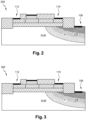
- FIG 2 is a sectional view representing a lateral bipolar transistor 200 according to a variant of the embodiment of the figure 1 , which differs in that a substrate zone 208 located at least under the NO-SO region 106, and preferably under the collector region 116, is doped N with a doping which can be gradual, decreasing radially at from the NW-SW region, for example according to a Gaussian profile.
- FIG. 3 is a sectional view representing a lateral bipolar transistor 300 according to another variant of the embodiment of the figure 1 , which differs in that a substrate zone 308 located at least under the NO-SO region 106, and preferably under the collector region 116, is doped P, with a doping which can be gradual, decreasing radially from the NW-SW region, for example according to a Gaussian profile.
- the lateral bipolar transistor is therefore constructed asymmetrically and comprises a NO-SO region positioned laterally near the collector region, said regions being separated laterally by an insulating trench.
- a bias to the substrate via a contact on the NW-SO region, characteristics of said transistor can be controlled.
- the polarization of the substrate makes it possible to modulate the "electrostatic" doping, that is to say to modulate the charge by electrostatic effect (electrostatic coupling with the regions of the transistor), of the lightly doped sub-region of the collector, or even the base region to a lesser extent, by a "back-biasing" technique, that is to say passing through the substrate, as illustrated in the figure 1 by the dotted arrows.
- the bias voltage applied to the substrate can for example be a few volts, positive or negative, for example between approximately 0.5 and 2 volts, depending on the thickness of the insulator 104.
- the bias voltage applied to the substrate can be reduced, even when it is also desired to modulate the base region by the polarization of the substrate. It is therefore advantageous to combine FD-SOI technology with substrate polarization.
- the asymmetric character of the collector with respect to the emitter region, which is both a doping asymmetry ("on average" collector region less doped than the emitter region) and a geometric asymmetry (region collector region wider than the emitter region) allows on the one hand to have sufficiently low doping of the collector region.
- the inventors determined that the electrostatic doping of the collector was more effective if the initial doping of said collector was weaker, or even much weaker, than in a symmetrical bipolar transistor.
- the collector doping is between 1.10 16 and 1.10 18 at/cm 3 for a transistor lateral bipolar according to one embodiment, to be compared with values of the order of 1.10 19 to 1.10 21 at/cm 3 for a symmetrical bipolar transistor.
- the influence of the electrostatic coupling of the substrate with the regions of the transistor is directly linked to the level of charges present in each region and therefore to the doping of each region.
- the access, or extrinsic, regions (heavily doped) of the transistor, corresponding to the second emitter sub-region 112b and the second collector sub-region 116b, as well as the heavily doped intrinsic region, corresponding to the first emitter sub-region 112a will be very little impacted by the electrostatic coupling of the substrate.
- Only the base region 114 (intrinsic) and the intrinsic collector region, corresponding to the first collector sub-region 116a (weakly doped) will be impacted by the electrostatic coupling of the substrate.
- the doping of the intrinsic collector 116a is much lower than that of the intrinsic base region 114, the electrostatic coupling will have a preponderant effect on the intrinsic collector region 116a.
- the inventors have determined that, while back-biasing impacts primarily, and homogeneously, along the vertical direction Z in the intrinsic manifold 116a, the effect of back-biasing can also reach the interface of the base region 114 with the insulator 104.
- a very lightly doped intrinsic collector 116a associated with the substrate 102 and insulator 104 assembly allows modulation of the effective doping or the charge in said intrinsic collector by electrostatic effect by applying a voltage to the NO-SO region 106 of the substrate 102. will see more after that this allows, for example, to switching the transistor from a very fast operating mode to a high voltage operating mode.
- the inventors determined that the electrostatic doping of the collector was more effective if the width of the collector region was larger, in order to favor the modulation of the electrostatic doping of the collector more than that of the base region.
- the principle is indeed to modulate the electrostatic doping of the collector region, and, to a lesser extent, that of the base region.
- a lateral bipolar transistor makes it possible to obtain different compromises between speed (frequency) and breakdown voltage (avalanche) for the same transistor, or even to improve the compromise between speed and breakdown voltage for the same transistor .
- a positive bias of the substrate can be applied to increase the speed of the transistor, corresponding to a configuration with a base region of small width and/or a heavily doped collector region, as will be seen in the description of the Figure 6 and some figure 8 .
- a negative bias of the substrate can be applied to increase the breakdown voltage, corresponding to a larger base region and/or lightly doped collector region configuration, reducing the electric field in the collector and thus repelling breakdown at a higher voltage, as will be seen in the description of the Figure 7 .
- FIGS. 4A to 4F are sectional views representing steps of an example of a process for manufacturing a lateral bipolar transistor, described with reference to transistor 100 of the figure 1 .
- an SOI substrate preferably an FD-SOI
- a substrate 102 made of a semiconductor
- an insulator 104 created in the substrate 102 using, for example, a SIMOX process or a SMARTCUT process
- a thin layer of monocrystalline silicon 110 (Si) on the insulator 104 For example, the substrate 102 is based on silicon.
- the insulator 104 may be an oxide (BOX), for example based on silicon dioxide (SiO 2 ).
- the thin layer of silicon 110 has a thickness of between a few nanometers and around fifteen nanometers, for example between 5 and 15 nm.
- the insulating layer 104 has a thickness of between a few nanometers and a few tens of nanometers, for example between 10 and 50 nm.
- FIG. 4A represents a structure obtained at the end of a step of forming insulating trenches (STI) 122a, 122b from the thin layer of silicon 110 up to a certain depth, for example between approximately 30 and 300 nm, in the substrate layer 102.
- STI insulating trenches
- Such insulating trenches can be formed by etching then filling the etched parts with an electrical insulating material.
- the insulating material is for example an oxide, such as silicon oxide.
- the method comprises a step of forming a substrate region 106 without SOI, or NO-SO region, in which the silicon layer 110 and the insulating layer 104 have been etched, according to techniques known to the person of the art, in order to access the substrate layer 102.
- This NW-SO region is formed laterally on the other side of the first insulating trench 122a with respect to the collector region 116.
- a selective epitaxy step can be carried out after etching in order to maintain a flat surface in the NW-SO region.
- the method may include a step of forming the base region 114 in SiGe, in the thin layer of silicon 110.
- a condensation technique which consists of depositing, on a portion of the thin layer of Si intended to form the base region, a layer of SiGe.
- This SiGe layer can be deposited by selective epitaxy, using a hard mask made of a dielectric material, for example SiO 2 , formed on the thin layer of Si prior to the deposition of SiGe.
- This hard mask includes a hole at the portion of the thin Si layer intended to form the base region.
- an oxidation step is carried out at a temperature of approximately 700°C and 900°C. During this step, germanium from the SiGe layer diffuses into the thin Si layer.
- the hard mask is then removed, for example by a suitable chemical treatment.
- FIG. 4B represents a structure obtained at the end of these stages of formation of the NW-SO region 106 and formation of the base region 114 in SiGe.
- This hard mask 126 comprises a hole 126c positioned to the right of the base region 114, the width of said hole corresponding substantially to the width of the extrinsic base 118 formed on said base region, and being substantially less than the width of the region of base.
- the hard mask 126 is formed by deposition of the dielectric material, then the hole 126c is formed by photolithography followed by etching.
- a step of selective epitaxy of boron-doped polysilicon is carried out in the hole 126c in order to form the extrinsic base 118.
- the boron of the polysilicon diffuses into the SiGe of the base region 114 in order to strongly dope in type P said base region (P+/SiGe).
- the hard mask 126 is partially removed to leave only a first portion of insulator 126a (first spacer) and a second portion of insulator 126b (second spacer) on either side of the extrinsic base 118, s extending respectively to the right of the first emitter sub-region 112a and the first collector sub-region 116a, that is to say stopping substantially at the edges of the portions of the thin silicon layer 110 not yet doped.
- FIG. 4F represents a structure obtained at the end of steps of forming portions of silicide 130 on the second emitter subregion 112b, the second emitter subregion 116b, on the extrinsic base 118 and on at least one portion of the NW-SO region 106, as well as steps of forming electrical contact points 140 on these silicide portions.
- silicided can advantageously be provided a zone 108 of strong N+ or P+ doping. All these steps are not detailed here, being within the reach of those skilled in the art.
- zone 108 can be doped N+.
- zone 108 can be doped P+.
- the asymmetric lateral bipolar transistor of the embodiments can be easily fabricated from a standard CMOS process, without adding additional process complexity. This makes it possible in particular to produce a low-cost bipolar transistor, while improving performance compared to other known bipolar transistors.
- FIG. 5 is a sectional view showing an example of a symmetrical bipolar transistor 500.
- the emitter 512 and collector 516 regions have substantially the same widths L12, L16 and substantially identical doping. In other words, the distance between the collector 516 and the base 514 is substantially equal to the distance between the emitter 512 and the base 514.
- FIG. 6 represents curves giving the current gain transition frequency (f T ) (curves 300, 302, 304, 306) and the maximum oscillation frequency (f max ) (curves 301, 303, 305, 307) as a function of collector current (I C ), for several substrate bias values (V SUB ), and for several examples of lateral bipolar transistors: curves 300 and 301 correspond to the symmetrical transistor 500, curves 302 and 303 correspond to the asymmetrical transistor 100, curves 304 and 305 correspond to the asymmetric transistor 200 with N doping, and the curves 306 and 307 correspond to the asymmetric transistor 300 with P doping; the curves 300a, 301a, 302a, 303a, 304a, 305a, 306a, 307a correspond to a polarization value (V SUB ) of 2V; curves 300b, 301b, 302b, 303b, 304b, 305b, 306b, 307b correspond to a polar
- FIG. 7 represents I(V) curves giving the collector current (collector current I) as a function of the collector voltage (collecter voltage V), for several substrate bias values (V SUB ), and for several examples of lateral bipolar transistors: curves 401 correspond to the symmetrical transistor 500, curves 403 correspond to the asymmetrical transistor 100, curves 405 correspond to the asymmetrical transistor 200 with N doping, and curves 407 correspond to the asymmetrical transistor 300 with P doping; the curves 401a, 403a, 405a, 407a correspond to a polarization value (V SUB ) of 2V; curves 401b, 403b, 405b, 407b correspond to a polarization value (V SUB ) of 0V (no polarization); and the curves 401c, 403c, 405c, 407c correspond to a polarization value (V SUB ) of -2V.
- curves 501 correspond to symmetrical transistor 500, and curves 503 correspond to asymmetric transistor 100; curves 501a, 503a correspond to a polarization value (V SUB ) of 2V; curves 501b, 503b correspond to a polarization value (V SUB ) of 0V (no polarization); and the curves 501c, 503c correspond to a polarization value (V SUB ) of -2V.
- the curves of figures 6 And 7 were plotted by comparing the asymmetrical side transistors 100, 200, 300 and the symmetrical side transistor 500, and the curves of the figure 8 were plotted by comparing the asymmetric side transistor 100 and the symmetric side transistor 500.
- the germanium concentration in the SiGe alloy of the base region is approximately 20% and the dopings of the different regions, for each transistors 100, 200, 300, 500 are those indicated in table 1 below.
- a positive bias of the substrate can be applied to increase the speed of the transistor.
- a positive polarization (curve 503a) causes a shift of the base-collector space charge zone towards the base, implying a smaller neutral base width, and a more highly electrostatically doped collector region, thus repelling the effects of strong injection at higher current densities.
- the base-emitter junction capacitance is reduced by the reduction of holes in the base.
- a transistor, or several transistors, according to one embodiment can be integrated into an electronic circuit 900, as illustrated in the Figure 9 , representing two asymmetrical lateral bipolar transistors 100 according to one embodiment each with a NO-SO region on the same SUB substrate (transistors represented very schematically). These may be several substantially similar transistors, but to which different bias voltages are applied. It can also be several different transistors, with the same bias voltages or different bias voltages.
- the electronic circuit may include other electronic components.
- the preferred, although non-limiting, applications of the transistor according to one embodiment are in systems requiring both dense digital functions and RF (Radio-Frequency) functions, for example 5G or 6G infrastructures, or radars, in particular long-range automobile radars, and more generally communication systems, whether by optical fiber or wireless, including portable systems but also millimeter imaging systems.
- RF Radio-Frequency
- a particularly advantageous application of the transistor according to one embodiment concerns Bi-CMOS (bipolar complementary metal-oxide-semiconductor) devices, which combine bipolar and CMOS transistors on the same integrated circuit chip, thus benefiting from both the characteristics high speed of bipolar technology and low consumption characteristics of CMOS technology.
- Bi-CMOS bipolar complementary metal-oxide-semiconductor
- the transistor may be another heterojunction lateral bipolar transistor (HBT), or a homojunction lateral bipolar transistor (BJT).
- HBT heterojunction lateral bipolar transistor
- BJT homojunction lateral bipolar transistor
Abstract
La présente description concerne un transistor bipolaire latéral (100) comprenant :- une région d'émetteur (112) dopée d'un premier type de conductivité et présentant une première largeur (L12) ;- une région de collecteur (116) dopée du premier type de conductivité, présentant une deuxième largeur (L16) supérieure à la première largeur et une concentration moyenne de dopage inférieure à la concentration moyenne de dopage de la région d'émetteur ;- une région de base (114) entre les régions d'émetteur et de collecteur dopée du deuxième type de conductivité; lesdites régions étant disposées dans une couche de silicium (110) sur une couche d'isolant (104) sur un substrat (102) ;- une région de substrat (106) dépourvue des couches de silicium et d'isolant, et positionnée du côté de la région de collecteur (116) ; et- un circuit de polarisation (150) relié, et adapté à fournir, à la région de substrat une tension de polarisation de manière à moduler le dopage électrostatique de la région de collecteur.The present description relates to a lateral bipolar transistor (100) comprising: - an emitter region (112) doped with a first conductivity type and having a first width (L12); - a collector region (116) doped with the first type of conductivity, having a second width (L16) greater than the first width and an average doping concentration lower than the average doping concentration of the emitter region; - a base region (114) between the emitter regions and collector doped with the second type of conductivity; said regions being arranged in a silicon layer (110) on an insulator layer (104) on a substrate (102); - a substrate region (106) devoid of the silicon and insulator layers, and positioned on the side from the collector region (116); and- a bias circuit (150) connected, and adapted to supply, to the substrate region a bias voltage so as to modulate the electrostatic doping of the collector region.
Description
La présente description concerne de façon générale les composants électroniques et plus précisément les transistors bipolaires et leur procédé de fabrication. La présente description concerne en particulier les transistors bipolaires latéraux, et des circuits électroniques comprenant au moins un transistor bipolaire latéral.This description generally concerns electronic components and more specifically bipolar transistors and their manufacturing process. The present description relates in particular to lateral bipolar transistors, and electronic circuits comprising at least one lateral bipolar transistor.
Un transistor bipolaire est un composant électronique à base de semiconducteur de la famille des transistors. Son principe de fonctionnement est basé sur deux jonctions PN, l'une en direct et l'autre en inverse, les deux jonctions étant formées par une région de base comprise entre une région d'émetteur et une région de collecteur.A bipolar transistor is an electronic component based on a semiconductor from the transistor family. Its operating principle is based on two PN junctions, one forward and the other reverse, the two junctions being formed by a base region between an emitter region and a collector region.
Un transistor bipolaire latéral est un transistor bipolaire dans lequel les régions d'émetteur, de base et de collecteur sont disposées l'une à côté de l'autre dans, et dans certains cas sur, un substrat de semiconducteur, à la différence d'un transistor bipolaire vertical où ces régions sont disposées l'une sur l'autre. Un transistor bipolaire latéral est bien adapté à l'intégration dans un procédé CMOS (Complementary Métal Oxide Semiconductor), par exemple en raison de nombreuses similitudes structurelles entre un transistor bipolaire latéral et un transistor à effet de champ à grille isolée (MOSFET, metal-oxide-semiconductor field-effect transistor).A lateral bipolar transistor is a bipolar transistor in which the emitter, base, and collector regions are arranged next to each other in, and in some cases on, a semiconductor substrate, unlike a vertical bipolar transistor where these regions are arranged one on top of the other. A lateral bipolar transistor is well suited for integration into a Complementary Metal Oxide Semiconductor (CMOS) process, for example due to many structural similarities between a lateral bipolar transistor and an insulated gate field effect transistor (MOSFET, metal- oxide-semiconductor field-effect transistor).
Dans certaines applications, il est recherché l'amélioration de caractéristiques d'un transistor bipolaire latéral, par exemple l'augmentation de sa rapidité de commutation et/ou de sa tension de claquage, pour lesquels on recherche généralement le meilleur compromis pour l'application visée.In certain applications, it is sought to improve the characteristics of a lateral bipolar transistor, for example the increase in its switching speed and/or its breakdown voltage, for which we generally seeks the best compromise for the intended application.
Un mode de réalisation pallie tout ou partie des inconvénients des transistors bipolaires connus, en particulier des transistors bipolaires latéraux connus.One embodiment overcomes all or part of the drawbacks of known bipolar transistors, in particular known lateral bipolar transistors.
Un mode de réalisation prévoit un transistor bipolaire latéral comprenant :
- une région d'émetteur dopée d'un premier type de conductivité et présentant une première largeur ;
- une région de collecteur dopée du premier type de conductivité, présentant une deuxième largeur supérieure à la première largeur de la région d'émetteur et une concentration moyenne de dopage inférieure à la concentration moyenne de dopage de la région d'émetteur ;
- une région de base dopée du deuxième type de conductivité et positionnée latéralement entre la région d'émetteur et la région de collecteur ;
lesdites régions d'émetteur, de base et de collecteur étant disposées dans une couche de silicium sur une couche d'isolant, ladite couche d'isolant étant sur un substrat semiconducteur ; - une région de substrat dépourvue de la couche de silicium et de la couche d'isolant, et positionnée latéralement du côté de la région de collecteur ; et
- un circuit de polarisation relié à la région de substrat, et adapté à fournir à ladite région de substrat une tension de polarisation de manière à moduler le dopage électrostatique de la région de collecteur.
- an emitter region doped with a first conductivity type and having a first width;
- a collector region doped with the first conductivity type, having a second width greater than the first width of the emitter region and an average doping concentration lower than the average doping concentration of the emitter region;
- a base region doped with the second conductivity type and positioned laterally between the emitter region and the collector region;
said emitter, base and collector regions being disposed in a silicon layer on an insulator layer, said insulator layer being on a semiconductor substrate; - a substrate region devoid of the silicon layer and the insulator layer, and positioned laterally on the collector region side; And
- a bias circuit connected to the substrate region, and adapted to supply said substrate region with a bias voltage so as to modulate the electrostatic doping of the collector region.
Selon un mode de réalisation, le transistor comprend une base extrinsèque présentant une troisième largeur et disposée sur la région de base présentant une quatrième largeur.According to one embodiment, the transistor comprises an extrinsic base having a third width and arranged on the base region having a fourth width.
Selon un mode de réalisation particulier, la troisième largeur de la base extrinsèque est inférieure à la quatrième largeur de la région de base, la base extrinsèque étant par exemple sensiblement centrée par rapport à la région de base.According to a particular embodiment, the third width of the extrinsic base is less than the fourth width of the base region, the extrinsic base being for example substantially centered relative to the base region.
Selon un mode de réalisation, le transistor comprend une première portion d'isolant sur une première portion de la région d'émetteur et une deuxième portion d'isolant sur une première portion de la région de collecteur, la région de base étant entre la première portion de la région d'émetteur et la première portion de la région de collecteur, et la base extrinsèque étant entre la première portion d'isolant et la deuxième portion d'isolant.According to one embodiment, the transistor comprises a first portion of insulator on a first portion of the emitter region and a second portion of insulator on a first portion of the collector region, the base region being between the first portion of the emitter region and the first portion of the collector region, and the extrinsic base being between the first insulator portion and the second insulator portion.
Selon un mode de réalisation, la couche de silicium a une épaisseur comprise entre quelques nanomètres et une quinzaine de nanomètres, par exemple entre 5 et 15 nanomètres.According to one embodiment, the silicon layer has a thickness of between a few nanometers and around fifteen nanometers, for example between 5 and 15 nanometers.
Selon un mode de réalisation, la couche d'isolant a une épaisseur comprise entre quelques nanomètres et quelques dizaines de nanomètres, par exemple entre 10 et 50 nanomètres.According to one embodiment, the insulating layer has a thickness of between a few nanometers and a few tens of nanometers, for example between 10 and 50 nanometers.
Selon un mode de réalisation, la région d'émetteur est formée par une région fortement dopée du premier type de conductivité.According to one embodiment, the emitter region is formed by a heavily doped region of the first conductivity type.
Selon un mode de réalisation, la région de collecteur comprend une première sous-région légèrement dopée du premier type de conductivité et une deuxième sous-région fortement dopée du premier type de conductivité.According to one embodiment, the collector region comprises a first sub-region lightly doped with the first conductivity type and a second sub-region heavily doped with the first conductivity type.
Selon un mode particulier de réalisation, la première sous-région de la région de collecteur est entre la région de base et la deuxième sous-région de la région de collecteur.According to a particular embodiment, the first sub-region of the collector region is between the base region and the second sub-region of the collector region.
Selon un mode particulier de réalisation, la première sous-région de la région de collecteur a une concentration moyenne de dopage en le premier type de conductivité inférieure à la concentration moyenne de dopage de la région de base en le deuxième type de conductivité, par exemple d'un facteur d'au moins dix.According to a particular embodiment, the first sub-region of the collector region has an average doping concentration of the first type of conductivity lower than the average doping concentration of the region basic in the second type of conductivity, for example by a factor of at least ten.
Selon un mode de réalisation, la région de base comprend un alliage silicium et germanium.According to one embodiment, the base region comprises a silicon and germanium alloy.
Selon un mode de réalisation, le transistor comprend une première tranchée isolante traversant la couche de silicium, la couche d'isolant et, partiellement, le substrat semiconducteur, ladite première tranchée isolante étant positionnée latéralement entre la région de collecteur et la région de substrat.According to one embodiment, the transistor comprises a first insulating trench passing through the silicon layer, the insulating layer and, partially, the semiconductor substrate, said first insulating trench being positioned laterally between the collector region and the substrate region.
Selon un mode de réalisation, le transistor comprend une deuxième tranchée isolante traversant la couche de silicium, la couche d'isolant et, partiellement, le substrat semiconducteur, la région d'émetteur étant positionnée latéralement entre ladite deuxième tranchée isolante et la région de base.According to one embodiment, the transistor comprises a second insulating trench passing through the silicon layer, the insulating layer and, partially, the semiconductor substrate, the emitter region being positioned laterally between said second insulating trench and the base region .
Selon un mode de réalisation, une zone du substrat située au moins sous la région de substrat dépourvue de la couche de silicium et de la couche d'isolant, et de préférence sous la région de collecteur, est dopée, par exemple avec un dopage graduel décroissant radialement depuis ladite région du substrat.According to one embodiment, an area of the substrate located at least under the substrate region devoid of the silicon layer and the insulating layer, and preferably under the collector region, is doped, for example with gradual doping decreasing radially from said region of the substrate.
Selon un mode de réalisation, le transistor comprend des prises de contact sur la région d'émetteur, la région de collecteur, la région de substrat, et, dans certains cas, sur la base extrinsèque, le circuit de polarisation étant relié à la région de substrat par une desdites prises de contact, une portion de siliciure étant par exemple formée sous chaque prise de contact.According to one embodiment, the transistor includes contacts on the emitter region, the collector region, the substrate region, and, in some cases, on the extrinsic base, the bias circuit being connected to the region of substrate by one of said contact points, a portion of silicide being for example formed under each contact point.
Un mode de réalisation prévoit un procédé de fabrication d'un transistor bipolaire, ledit procédé comprenant :
- la fourniture d'une couche de silicium sur une couche d'isolant, sur un substrat semiconducteur ;
- la formation, dans la couche de silicium, d'une région d'émetteur d'une première largeur dopée d'un premier type de conductivité ; d'une région de collecteur dopée du premier type de conductivité avec une deuxième largeur supérieure à la première largeur et une concentration moyenne de dopage inférieure à la concentration moyenne de dopage de la région d'émetteur ; et d'une région de base dopée du deuxième type de conductivité et formée latéralement entre ladite région d'émetteur et ladite région de collecteur ;
- la formation d'une région de substrat dépourvue de la couche de silicium et de la couche d'isolant, ladite région de substrat étant formée latéralement du côté de la région de collecteur ;
- la formation d'un circuit de polarisation relié à la région de substrat, et adapté à fournir à ladite région de substrat une tension de polarisation de manière à moduler le dopage électrostatique de la région de collecteur.
- providing a silicon layer on an insulator layer, on a semiconductor substrate;
- forming, in the silicon layer, an emitter region of a first width doped with a first conductivity type; a collector region doped with the first conductivity type with a second width greater than the first width and an average doping concentration lower than the average doping concentration of the emitter region; and a base region doped with the second conductivity type and formed laterally between said emitter region and said collector region;
- forming a substrate region devoid of the silicon layer and the insulator layer, said substrate region being formed laterally on the collector region side;
- forming a bias circuit connected to the substrate region, and adapted to supply said substrate region with a bias voltage so as to modulate the electrostatic doping of the collector region.
Selon un mode de réalisation, le procédé comprend, préalablement à la formation des régions d'émetteur, de base, de collecteur et de substrat :
- la formation d'une première tranchée isolante dans la couche de silicium, la couche d'isolant, et partiellement dans le substrat, ladite première tranchée isolante étant formée latéralement entre la région de collecteur et l'emplacement de la future région de substrat ; et
- la formation d'une deuxième tranchée isolante dans la couche de silicium, la couche d'isolant et partiellement dans le substrat, la région d'émetteur étant positionnée latéralement entre ladite deuxième tranchée isolante et la région de base.
- forming a first insulating trench in the silicon layer, the insulating layer, and partially in the substrate, said first insulating trench being formed laterally between the collector region and the location of the future substrate region; And
- forming a second insulating trench in the silicon layer, the insulating layer and partially in the substrate, the emitter region being positioned laterally between said second insulating trench and the base region.
Un mode de réalisation prévoit un procédé d'utilisation d'un transistor selon un mode de réalisation, ledit procédé comprenant l'application, par le circuit de polarisation, d'une tension de polarisation à la région de substrat.One embodiment provides a method of using a transistor according to one embodiment, said method comprising applying, by the bias circuit, a bias voltage to the substrate region.
Selon un mode de réalisation, le procédé d'utilisation comprend l'application d'une tension de polarisation positive à la région de substrat, de manière à augmenter la rapidité et/ou le gain du transistor.According to one embodiment, the method of use comprises applying a positive bias voltage to the substrate region, so as to increase the speed and/or gain of the transistor.
Selon un mode de réalisation, le procédé d'utilisation comprend l'application d'une tension de polarisation négative à la région de substrat, de manière à augmenter la tension de claquage du transistor.According to one embodiment, the method of use comprises applying a negative bias voltage to the substrate region, so as to increase the breakdown voltage of the transistor.
Un mode de réalisation prévoit un circuit électronique comprenant au moins un transistor selon un mode de réalisation.One embodiment provides an electronic circuit comprising at least one transistor according to one embodiment.
Un mode de réalisation prévoit un circuit électronique comprenant plusieurs transistors selon un mode de réalisation, au moins deux transistors ayant des tensions de polarisation différentes appliquées à la région de substrat.One embodiment provides an electronic circuit comprising several transistors according to one embodiment, at least two transistors having different bias voltages applied to the substrate region.
Ces caractéristiques et avantages, ainsi que d'autres, seront exposés en détail dans la description suivante de modes de réalisation particuliers faite à titre non limitatif en relation avec les figures jointes parmi lesquelles :
- la
figure 1 est une vue en coupe représentant un transistor bipolaire latéral selon un mode de réalisation ; - la
figure 2 est une vue en coupe représentant un transistor bipolaire latéral selon une variante du mode de réalisation de lafigure 1 ; - la
figure 3 est une vue en coupe représentant un transistor bipolaire latéral selon une autre variante du mode de réalisation de lafigure 1 ; - la
figure 4A , lafigure 4B , lafigure 4C , lafigure 4D , lafigure 4E et lafigure 4F sont des vues en coupe représentant des étapes d'un procédé de fabrication d'un transistor bipolaire latéral selon un mode de réalisation ; - la
figure 5 est une vue en coupe représentant un transistor bipolaire symétrique ; - la
figure 6 représente des courbes donnant la fréquence de transition du gain en courant (fT) et la fréquence maximum d'oscillation (fmax) en fonction du courant de collecteur (Ic), et ce, pour plusieurs valeurs de polarisation du substrat (VSUB), et pour plusieurs exemples de transistors bipolaires latéraux ; - la
figure 7 représente des courbes I(V) donnant le courant de collecteur en fonction de la tension du collecteur, et ce, pour plusieurs valeurs de polarisation du substrat (VSUB), et pour plusieurs exemples de transistors bipolaires latéraux ; - la
figure 8 représente des courbes donnant la densité d'électrons et la densité de trous en fonction de la distance latérale par rapport à la jonction base/émetteur, et ce, pour plusieurs valeurs de polarisation du substrat (VSUB), et pour un transistor bipolaire latéral symétrique et un transistor bipolaire latéral asymétrique ; - la
figure 9 représente un circuit électronique comprenant plusieurs transistors bipolaires latéraux selon un mode de réalisation.
- there
figure 1 is a sectional view showing a lateral bipolar transistor according to one embodiment; - there
figure 2 is a sectional view representing a lateral bipolar transistor according to a variant of the embodiment of thefigure 1 ; - there
Figure 3 is a sectional view representing a lateral bipolar transistor according to another variant of the embodiment of thefigure 1 ; - there
Figure 4A , therefigure 4B , therefigure 4C , therefigure 4D , thereFigure 4E and thefigure 4F are sectional views representing steps of a method of manufacturing a lateral bipolar transistor according to one embodiment; - there
figure 5 is a sectional view showing a symmetrical bipolar transistor; - there
Figure 6 represents curves giving the current gain transition frequency (f T ) and the maximum oscillation frequency (f max ) as a function of the collector current (I c ), and this, for several substrate bias values (V SUB ), and for several examples of lateral bipolar transistors; - there
Figure 7 represents I(V) curves giving the collector current as a function of the collector voltage, for several substrate bias values (V SUB ), and for several examples of lateral bipolar transistors; - there
figure 8 represents curves giving the electron density and the hole density as a function of the lateral distance from the base/emitter junction, for several values of substrate polarization (V SUB ), and for a lateral bipolar transistor symmetrical and an asymmetrical lateral bipolar transistor; - there
Figure 9 represents an electronic circuit comprising several lateral bipolar transistors according to one embodiment.
De mêmes éléments ont été désignés par de mêmes références dans les différentes figures. En particulier, les éléments structurels et/ou fonctionnels communs aux différents modes de réalisation peuvent présenter les mêmes références et peuvent disposer de propriétés structurelles, dimensionnelles et matérielles identiques.The same elements have been designated by the same references in the different figures. In particular, the structural and/or functional elements common to the different embodiments may have the same references and may have identical structural, dimensional and material properties.
Par souci de clarté, seuls les étapes et éléments utiles à la compréhension des modes de réalisation décrits ont été représentés et sont détaillés. En particulier, toutes les étapes de fabrication et les détails des éléments d'un transistor bipolaire latéral, par exemple la formation de portions de siliciure (siliciuration, ou "salicidation" en anglais) sur des régions semiconductrices et/ou la prise de contact, ne sont pas détaillés, étant réalisables avec les procédés usuels connus de la personne du métier.For the sake of clarity, only the steps and elements useful for understanding the embodiments described have been represented and are detailed. In particular, all the manufacturing steps and the details of the elements of a lateral bipolar transistor, for example the formation of portions of silicide (silicide, or "salicidation" in English) on semiconductor regions and/or making contact, are not detailed, being achievable with the usual processes known to those skilled in the art.
Sauf précision contraire, lorsque l'on fait référence à deux éléments connectés entre eux, cela signifie directement connectés sans éléments intermédiaires autres que des conducteurs, et lorsque l'on fait référence à deux éléments reliés (en anglais "coupled") entre eux, cela signifie que ces deux éléments peuvent être connectés ou être reliés par l'intermédiaire d'un ou plusieurs autres éléments.Unless otherwise specified, when we refer to two elements connected to each other, this means directly connected without intermediate elements other than conductors, and when we refer to two elements connected (in English "coupled") to each other, this means that these two elements can be connected or be linked through one or more other elements.
Dans la description qui suit, lorsque l'on fait référence à des qualificatifs de position absolue, tels que les termes "avant", "arrière", "haut", "bas", "gauche", "droite", etc., ou relative, tels que les termes "dessus", "dessous", "supérieur", "inférieur", etc., ou à des qualificatifs d'orientation, tels que les termes "horizontal", "vertical", etc., il est fait référence sauf précision contraire à l'orientation des figures ou à un transistor bipolaire latéral dans une position normale d'utilisation.In the following description, when referring to absolute position qualifiers, such as "front", "back", "up", "down", "left", "right", etc., or relative, such as the terms "above", "below", "superior", "lower", etc., or to qualifiers of orientation, such as the terms "horizontal", "vertical", etc., it Unless otherwise specified, reference is made to the orientation of the figures or to a lateral bipolar transistor in a normal position of use.
Dans la description qui suit, une largeur ou une distance correspond à une dimension dans la direction latérale d'un transistor bipolaire latéral, qui correspond à la direction horizontale X repérée dans les figures, et une épaisseur ou une profondeur correspond à une dimension dans la direction verticale Z repérée dans les figures.In the following description, a width or a distance corresponds to a dimension in the lateral direction of a lateral bipolar transistor, which corresponds to the horizontal direction vertical direction Z marked in the figures.
Sauf précision contraire, les expressions "environ", "approximativement", "sensiblement", et "de l'ordre de" signifient à 10 % près, de préférence à 5 % près.Unless otherwise specified, the expressions "approximately", "approximately", "substantially", and "of the order of" mean to the nearest 10%, preferably to the nearest 5%.
Les modes de réalisation représentés sur les figures, et décrits dans la description qui suit, comportent un transistor bipolaire latéral de type NPN, le dopage N correspondant au premier type de conductivité, et le dopage P au deuxième type de conductivité.The embodiments shown in the figures, and described in the description which follows, comprise a lateral bipolar transistor of the NPN type, the N doping corresponding to the first type of conductivity, and the P doping to the second type of conductivity.
Cependant, la personne du métier comprendra facilement que les principes décrits dans la présente description peuvent également être appliqués à un transistor bipolaire latéral de type PNP, le dopage P correspondant alors au premier type de conductivité, et le dopage N au deuxième type de conductivité.However, those skilled in the art will easily understand that the principles described in the present description can also be applied to a lateral bipolar transistor of the PNP type, the P doping then corresponding to the first type of conductivity, and the N doping to the second type of conductivity.
La
Le transistor 100 représenté est fabriqué en technologie SOI et comprend un substrat 102 (SUB), un isolant 104 créé dans le substrat 102 en utilisant, par exemple, un procédé SIMOX ou un procédé SMARTCUT, et une fine couche de silicium monocristallin (Si) 110 sur l'isolant 104. Par exemple, le substrat 102 est à base de silicium (Si). L'isolant 104 peut être un oxyde (BOX, de l'anglais Buried Oxide), par exemple à base de dioxyde de silicium (SiO2).The
De préférence, le transistor est en technologie dite "Fully-Depleted SOI" (FD-SOI), c'est-à-dire permettant de fonctionner en mode totalement déplété, en référence au fonctionnement des transistors CMOS FD-SOI.Preferably, the transistor is in so-called "Fully-Depleted SOI" (FD-SOI) technology, that is to say allowing it to operate in completely depleted mode, with reference to the operation of CMOS FD-SOI transistors.
De préférence, la fine couche de silicium 110 a une épaisseur e10 comprise entre quelques nanomètres et une quinzaine de nanomètres, par exemple entre 5 et 15 nm.Preferably, the thin layer of
De préférence, la couche d'isolant 104 a une épaisseur e4 comprise entre quelques nanomètres et quelques dizaines de nanomètres, par exemple entre 10 et 50 nm.Preferably, the insulating
Le transistor 100 comprend une région d'émetteur 112 dopé N, une région de collecteur 116 dopé N et une région de base 114 dopé P formée entre la région d'émetteur 112 et la région de collecteur 116.The
La région d'émetteur 112, la région de base 114 et la région de collecteur 116 sont formées latéralement l'une à côté de l'autre dans la couche de silicium 110, la région de base étant entre la région d'émetteur et la région de collecteur.The
La région d'émetteur 112 est fortement dopée N (N+), la région de base 114 est fortement dopée P (P+) et la région de collecteur 116 comprend une première sous-région de collecteur 116a légèrement dopée N (N-) et une deuxième sous-région de collecteur 116b fortement dopée N (N+), la première sous-région de collecteur 116a étant disposée entre la région de base 114 et la deuxième sous-région de collecteur 116b. Cette différence de dopage entre l'émetteur et le collecteur crée une asymétrie de dopage du transistor. En outre, la largeur L16 de la région de collecteur 116 est supérieure à la largeur L12 de la région d'émetteur 112, créant une asymétrie géométrique du transistor. Ainsi, le transistor 100 est dit asymétrique géométriquement et par le dopage. Par exemple, "fortement dopé" signifie avoir une concentration moyenne de dopage supérieure ou égale à 1,1019 at/cm3 et "légèrement dopé" signifie avoir une concentration moyenne de dopage inférieure à 1,1019 at/cm3.The
La portion de la couche de silicium correspondant à la région de base 114 peut être traitée afin de former un alliage silicium-germanium (SiGe) dans ladite région de base. Le germanium dans la base permet d'améliorer les performances du transistor, qui est alors de type hétérojonction (HBT, de l'anglais Heterojunction Bipolar Transistor). Par exemple, l'ajout de germanium dans la région de base peut réduire la tension entre la région d'émetteur et la région de base en raison de la bande interdite plus petite de l'alliage SiGe par rapport au silicium. Selon un mode alternatif, la région de base est en silicium, le transistor étant alors un transistor du type à homojonction (BJT, de l'anglais Bipolar Junction Transistor).The portion of the silicon layer corresponding to the
Cette région de base 114 correspond à une région de base dite "intrinsèque" (partie active de la base, comprise entre la région d'émetteur et la région de collecteur).This
Cette région de base intrinsèque est surmontée par une région de base dite "extrinsèque" 118, qui peut également être désignée par le terme de "base extrinsèque", et qui est une partie de connexion électrique, par l'intermédiaire de laquelle la région intrinsèque de base 114 peut être polarisée lors du fonctionnement du transistor. La base extrinsèque 118 est par exemple à base de silicium polycristallin, ou polysilicium (Poly).This intrinsic base region is surmounted by a so-called "extrinsic"
De préférence, la largeur L18 de la base extrinsèque 118 est inférieure à la largeur L14 de la région de base 114, et la base extrinsèque positionnée par rapport à la région de base de sorte que des première et deuxième portions 114a, 114b aux deux extrémités latérales de la région de base 114 ne soient pas recouvertes par la base extrinsèque 118.Preferably, the width L18 of the
Par exemple, la largeur L14 de la région de base 114 est comprise entre environ 10 et 100 nm, et la largeur L18 de la base extrinsèque 118 est comprise entre environ 5 et 90 nm, la base extrinsèque pouvant être sensiblement centrée par rapport à la région de base.For example, the width L14 of the
En outre, une portion 112a (première sous-région d'émetteur) de la région d'émetteur 112 et la première portion 114a de la région de base 114 non recouverte par la base extrinsèque 118 sont recouvertes par une première portion d'isolant 126a (ou premier espaceur), de préférence un oxyde, par exemple du SiO2. Similairement, une portion de la région de collecteur 116 et la deuxième portion 114b de la région de base 114 non recouverte par la base extrinsèque 118 sont recouvertes par une deuxième portion d'isolant 126b (ou deuxième espaceur), de préférence un oxyde, par exemple du SiO2. Ces espaceurs permettent d'isoler électriquement la base extrinsèque 118 de chacune des régions d'émetteur 112 et de collecteur 116. Le fait que les première 114a et deuxième 114b portions de la région de base 114 ne soient pas recouvertes par la base extrinsèque 118, mais soient recouvertes respectivement par les premier 126a et deuxième 126b espaceurs permet d'améliorer l'isolation de ladite base extrinsèque vis-à-vis de chacune des régions d'émetteur 112 et de collecteur 116.In addition, a
Des tranchées isolantes 122a, 122b sont formées (creusées puis remplies d'un isolant) dans la fine couche de silicium 110, dans l'isolant 104 et dans le substrat 102 sur une certaine profondeur, afin de séparer le transistor 100 de composants électroniques adjacents pouvant être mis en œuvre dans la couche de silicium 110. Plus précisément, les tranchées isolantes 122a, 122b traversent le substrat 102 partiellement, sur une épaisseur très inférieure à l'épaisseur dudit substrat, et peuvent être désignées par le terme anglosaxon "Shallow Trench Isolation" (STI). Elles peuvent être remplies d'un isolant oxyde, par exemple du SiO2. Une première tranchée isolante 122a est positionnée latéralement contre la région de collecteur 116, et dans le mode représenté contre la deuxième sous-région de collecteur 116b, et une deuxième tranchée isolante 122b est positionnée latéralement contre la région d'émetteur 112.Insulating
Par exemple, la largeur L16 de la région de collecteur 116 est comprise entre environ 30 et 400 nm ou entre environ 30 et 300 nm, la largeur L16a de la première sous-région de collecteur 116a est comprise entre environ 15 et 200 nm, la largeur L16b de la deuxième sous-région de collecteur 116b est comprise entre environ 15 et 200 nm, et la largeur L12 de la région d'émetteur 112 est comprise entre environ 15 et 200 nm.For example, the width L16 of the
Il est à noter que, dans les modes de réalisation décrits, la largeur L16 de la région de collecteur 116 correspond sensiblement à la distance entre la région de base 114 et la première tranchée isolante 122a, et la largeur L12 de la région d'émetteur 112 correspond sensiblement à la distance entre la deuxième tranchée isolante 122b et la région de base 114.It should be noted that, in the embodiments described, the width L16 of the
Dans le transistor 100 représenté en
Dans le transistor 100 représenté en
En outre, le transistor 100 comprend une région de substrat 106 dans laquelle, sur le substrat 102, la couche de silicium 110 et la couche d'isolant 104 ont été supprimées, par exemple gravées. Une telle région est connue par la personne du métier par le terme "région sans SOI" ou région "NO-SO". Cette région de substrat 106 est positionnée latéralement de l'autre côté de la première tranchée isolante 122a par rapport à la région de collecteur 116, et dans le mode représenté par rapport à la deuxième sous-région de collecteur 116b. En d'autres termes, la première tranchée isolante 122a est entre la région de collecteur 116 et la région NO-SO 106, permettant d'isoler latéralement ces deux régions l'une de l'autre. La région NO-SO 106 permet de contacter le substrat en vue de le polariser selon une technique dite de "back-biasing" (polarisation par le substrat) comme expliqué plus après.Furthermore, the
Sur l'autre portion 112b (deuxième sous-région d'émetteur) de la région d'émetteur 112 non recouverte par le premier espaceur 126a, sur la portion de la région de collecteur 116 non recouverte par le deuxième espaceur 126b, sur la base extrinsèque 118 et sur au moins une portion de la région NO-SO 106, peut être formée une portion de siliciure de métal 130 (désigné "siliciure"), et une prise de contact électrique 140 ou "contact" (les contacts sont visibles en
De préférence, comme représenté en
Le contact 140 sur la région NO-SO 106, de préférence recouverte de siliciure 130, permet d'appliquer à la région de collecteur 116 une tension de polarisation, de manière à moduler la charge par effet électrostatique dans la sous-région la plus faiblement dopée du collecteur, c'est-à-dire la première sous-région de collecteur 116a, comme expliqué plus après. Une telle polarisation peut être réalisée à l'aide d'un circuit de polarisation 150, comprenant par exemple une ligne de polarisation 151 reliée d'une part à un générateur de tension 152 et d'autre part à la région de substrat NO-SO via son contact 140 (circuit représenté en
La
La
Le transistor bipolaire latéral selon un mode de réalisation est donc construit de manière asymétrique et comprend une région NO-SO positionnée latéralement à proximité de la région de collecteur, lesdites régions étant séparées latéralement par une tranchée isolante. En appliquant une polarisation au substrat via un contact sur la région NO-SO, des caractéristiques dudit transistor peuvent être contrôlées. En particulier, la polarisation du substrat permet de moduler le dopage "électrostatique", c'est-à-dire de moduler la charge par effet électrostatique (couplage électrostatique avec les régions du transistor), de la sous-région faiblement dopée du collecteur, voire de la région de base dans une moindre mesure, par une technique de "back-biasing", c'est-à-dire en passant par le substrat, comme illustré dans la
La tension de polarisation appliquée au substrat peut par exemple être de quelques volts, en positif ou en négatif, par exemple entre environ 0,5 et 2 volts, et ce, en fonction de l'épaisseur de l'isolant 104.The bias voltage applied to the substrate can for example be a few volts, positive or negative, for example between approximately 0.5 and 2 volts, depending on the thickness of the
Avec un transistor bipolaire latéral en technologie "Fully-Depleted SOI" (FD-SOI), et par exemple dans les plages d'épaisseurs de couche Si et de couche d'isolant du SOI données plus avant, la tension de polarisation appliquée au substrat peut être réduite, même lorsqu'on souhaite aussi moduler la région de base par la polarisation du substrat. Il est donc avantageux de combiner la technologie FD-SOI avec la polarisation du substrat.With a lateral bipolar transistor in "Fully-Depleted SOI" (FD-SOI) technology, and for example in the Si layer and SOI insulating layer thickness ranges given below, the bias voltage applied to the substrate can be reduced, even when it is also desired to modulate the base region by the polarization of the substrate. It is therefore advantageous to combine FD-SOI technology with substrate polarization.
En outre, le caractère asymétrique du collecteur, par rapport à la région d'émetteur, qui est à la fois une asymétrie de dopage (région de collecteur "en moyenne" moins dopée que la région d'émetteur) et une asymétrie géométrique (région de collecteur plus large que la région d'émetteur) permet d'une part d'avoir un dopage de la région de collecteur suffisamment faible. En effet, les inventeurs ont déterminé que le dopage électrostatique du collecteur était plus efficace si le dopage initial dudit collecteur était plus faible, voire beaucoup plus faible, que dans un transistor bipolaire symétrique. Typiquement, le dopage du collecteur est compris entre 1.1016 et 1.1018 at/cm3 pour un transistor bipolaire latéral selon un mode de réalisation, à comparer avec des valeurs de l'ordre de 1.1019 à 1.1021 at/cm3 pour un transistor bipolaire symétrique.Furthermore, the asymmetric character of the collector, with respect to the emitter region, which is both a doping asymmetry ("on average" collector region less doped than the emitter region) and a geometric asymmetry (region collector region wider than the emitter region) allows on the one hand to have sufficiently low doping of the collector region. Indeed, the inventors determined that the electrostatic doping of the collector was more effective if the initial doping of said collector was weaker, or even much weaker, than in a symmetrical bipolar transistor. Typically, the collector doping is between 1.10 16 and 1.10 18 at/cm 3 for a transistor lateral bipolar according to one embodiment, to be compared with values of the order of 1.10 19 to 1.10 21 at/cm 3 for a symmetrical bipolar transistor.
L'influence du couplage électrostatique du substrat avec les régions du transistor est directement liée au niveau des charges présentes dans chaque région et donc au dopage de chaque région. Ainsi, les régions d'accès, ou extrinsèques, (fortement dopées) du transistor, correspondant à la deuxième sous-région d'émetteur 112b et à la deuxième sous-région de collecteur 116b, ainsi que la région intrinsèque fortement dopée, correspondant à la première sous-région d'émetteur 112a, ne seront que très peu impactées par le couplage électrostatique du substrat. Seules la région de base 114 (intrinsèque) et la région de collecteur intrinsèque, correspondant à la première sous-région de collecteur 116a (faiblement dopée), seront impactées par le couplage électrostatique du substrat. Aussi, si le dopage du collecteur intrinsèque 116a est très inférieur à celui de la région de base intrinsèque 114, le couplage électrostatique jouera de façon prépondérante sur la région de collecteur intrinsèque 116a.The influence of the electrostatic coupling of the substrate with the regions of the transistor is directly linked to the level of charges present in each region and therefore to the doping of each region. Thus, the access, or extrinsic, regions (heavily doped) of the transistor, corresponding to the
En outre, les inventeurs ont déterminé que, si le back-biasing a un impact principalement, et de façon homogène, le long de la direction verticale Z dans le collecteur intrinsèque 116a, l'effet du back-biasing peut également atteindre l'interface de la région de base 114 avec l'isolant 104.Furthermore, the inventors have determined that, while back-biasing impacts primarily, and homogeneously, along the vertical direction Z in the
Un collecteur intrinsèque 116a très faiblement dopé associé à l'ensemble substrat 102 et isolant 104 permet une modulation du dopage effectif ou de la charge dans ledit collecteur intrinsèque par effet électrostatique en appliquant une tension sur la région NO-SO 106 du substrat 102. On verra plus après que cela permet, par exemple, de commuter le transistor d'un mode de fonctionnement très rapide à un mode de fonctionnement à forte tension.A very lightly doped
D'autre part, les inventeurs ont déterminé que le dopage électrostatique du collecteur était plus efficace si la largeur de la région de collecteur était plus grande, afin de favoriser davantage la modulation du dopage électrostatique du collecteur que celle de la région de base. Le principe est en effet bien de moduler le dopage électrostatique de la région de collecteur, et, dans une moindre mesure, celui de la région de base.On the other hand, the inventors determined that the electrostatic doping of the collector was more effective if the width of the collector region was larger, in order to favor the modulation of the electrostatic doping of the collector more than that of the base region. The principle is indeed to modulate the electrostatic doping of the collector region, and, to a lesser extent, that of the base region.
Il est à noter que l'efficacité du dopage électrostatique peut également dépendre du dopage du substrat, comme expliqué plus après.It should be noted that the effectiveness of electrostatic doping can also depend on the doping of the substrate, as explained later.
On verra dans la description des
Selon un exemple, une polarisation positive du substrat peut être appliquée pour augmenter la rapidité du transistor, correspondant à une configuration à région de base de faible largeur et/ou à région de collecteur fortement dopée, comme on le verra dans la description de la
Selon un autre exemple, une polarisation négative du substrat peut être appliquée pour augmenter la tension de claquage, correspondant à une configuration à région de base plus large et/ou à région de collecteur faiblement dopée, réduisant le champ électrique dans le collecteur et ainsi repoussant le claquage à une plus haute tension, comme on le verra dans la description de la
Selon un exemple de réalisation pouvant s'appliquer aux transistors 100, 200, 300, on considère les dimensions suivantes, données à 10 % près, de préférence à 5 % près :
- largeur totale région d'émetteur (L12) : 60 nm ;
- largeur région d'émetteur siliciurée (L12') : 30 nm ;
- largeur totale région de collecteur (L16) : 60 nm ;
- largeur première sous-région de collecteur (L16a) : 30 nm ;
- largeur deuxième sous-région de collecteur (L16b) : 30 nm ;
- largeur région de collecteur siliciurée (L16') : 30 nm ;
- largeur région de base (L14) : 28 nm ;
- largeur base extrinsèque (L18) : 20 nm ;
- largeur tranchées isolantes (L22) : 30 nm ;
- épaisseur couche de silicium (e10) : 7 nm ;
- épaisseur couche d'isolant (e4) : 25 nm ;
- épaisseur base extrinsèque (e18) : 20 nm ;
- profondeur tranchées isolantes (e22) : 32 nm.
- total width of emitter region (L12): 60 nm;
- width of silicide emitter region (L12'): 30 nm;
- total width of collector region (L16): 60 nm;
- first collector subregion width (L16a): 30 nm;
- width second collector subregion (L16b): 30 nm;
- width of silicide collector region (L16'): 30 nm;
- base region width (L14): 28 nm;
- extrinsic base width (L18): 20 nm;
- width of insulating trenches (L22): 30 nm;
- silicon layer thickness (e10): 7 nm;
- insulating layer thickness (e4): 25 nm;
- extrinsic base thickness (e18): 20 nm;
- depth of insulating trenches (e22): 32 nm.
Les
On part d'un substrat SOI, de préférence un FD-SOI, comprenant un substrat 102 (SUB) en un semiconducteur, un isolant 104 créé dans le substrat 102 en utilisant, par exemple, un procédé SIMOX ou un procédé SMARTCUT, et une fine couche de silicium monocristallin 110 (Si) sur l'isolant 104. Par exemple, le substrat 102 est à base de silicium. L'isolant 104 peut être un oxyde (BOX), par exemple à base de dioxyde de silicium (SiO2).We start from an SOI substrate, preferably an FD-SOI, comprising a substrate 102 (SUB) made of a semiconductor, an
De préférence, la fine couche de silicium 110 a une épaisseur comprise entre quelques nanomètres et une quinzaine de nanomètres, par exemple entre 5 et 15 nm.Preferably, the thin layer of
De préférence, la couche d'isolant 104 a une épaisseur comprise entre quelques nanomètres et quelques dizaines de nanomètres, par exemple entre 10 et 50 nm.Preferably, the insulating
La
De telles tranchées isolantes peuvent être formées par gravure puis remplissage, par un matériau isolant électrique, des parties gravées. Le matériau isolant est par exemple un oxyde, tel qu'un oxyde de silicium.Such insulating trenches can be formed by etching then filling the etched parts with an electrical insulating material. The insulating material is for example an oxide, such as silicon oxide.
Ensuite, le procédé comprend une étape de formation d'une région de substrat 106 sans SOI, ou région NO-SO, dans laquelle la couche de silicium 110 et la couche d'isolant 104 ont été gravées, selon les techniques connues de la personne du métier, afin d'accéder à la couche de substrat 102. Cette région NO-SO est formée latéralement de l'autre côté de la première tranchée isolante 122a par rapport à la région de collecteur 116.Then, the method comprises a step of forming a
Selon un mode de réalisation, une étape d'épitaxie sélective peut être réalisée après gravure afin de garder une surface plane sur la région NO-SO.According to one embodiment, a selective epitaxy step can be carried out after etching in order to maintain a flat surface in the NW-SO region.
En outre, le procédé peut comprendre une étape de formation de la région de base 114 en SiGe, dans la fine couche de silicium 110.In addition, the method may include a step of forming the
Plusieurs techniques connues de la personne du métier existent pour former une région en SiGe dans une couche de Si. On peut citer, par exemple, une technique de condensation qui consiste à déposer, sur une portion de la fine couche de Si destinée à former la région de base, une couche de SiGe. Cette couche de SiGe peut être déposée par épitaxie sélective, à l'aide d'un masque dur en un matériau diélectrique, par exemple du SiO2, formé sur la fine couche de Si préalablement au dépôt de SiGe. Ce masque dur comprend un trou au niveau de la portion de la fine couche de Si destinée à former la région de base. Ensuite, on effectue une étape d'oxydation à une température d'environ 700°C et 900°C. Durant cette étape, du germanium de la couche de SiGe diffuse dans la fine couche de Si. Le masque dur est ensuite enlevé, par exemple par un traitement chimique adapté.Several techniques known to those skilled in the art exist for forming a SiGe region in a layer of Si. We can cite, for example, a condensation technique which consists of depositing, on a portion of the thin layer of Si intended to form the base region, a layer of SiGe. This SiGe layer can be deposited by selective epitaxy, using a hard mask made of a dielectric material, for example SiO 2 , formed on the thin layer of Si prior to the deposition of SiGe. This hard mask includes a hole at the portion of the thin Si layer intended to form the base region. Then, an oxidation step is carried out at a temperature of approximately 700°C and 900°C. During this step, germanium from the SiGe layer diffuses into the thin Si layer. The hard mask is then removed, for example by a suitable chemical treatment.
La
La
- une première sous-région 112a d'émetteur fortement dopée N (N+/Si) ; et
- une première sous-région 116a de collecteur faiblement dopée N (N-/Si).
- a first heavily N-doped
emitter subregion 112a (N+/Si); And - a
first subregion 116a of lightly doped N collector (N-/Si).
Ensuite, un masque dur 126 en un matériau diélectrique, par exemple à base de TétraEthOxySilane (TEOS) pour former du SiO2, est formé sur la fine couche de silicium 110 (partiellement dopée) et sur les tranchées isolantes 122a, 122b. Ce masque dur 126 comprend un trou 126c positionné au droit de la région de base 114, la largeur dudit trou correspondant sensiblement à la largeur de la base extrinsèque 118 formée sur ladite région de base, et étant sensiblement inférieure à la largeur de la région de base. Par exemple, le masque dur 126 est formé par dépôt du matériau diélectrique, puis le trou 126c est formé par photolithographie suivie d'une gravure.Then, a
Une étape d'épitaxie sélective de polysilicium dopé bore (P+/Poly) est réalisée dans le trou 126c afin de former la base extrinsèque 118. Le bore du polysilicium vient diffuser dans le SiGe de la région de base 114 afin de doper fortement en type P ladite région de base (P+/SiGe).A step of selective epitaxy of boron-doped polysilicon (P+/Poly) is carried out in the
La
Ensuite, le masque dur 126 est partiellement retiré pour ne laisser qu'une première portion d'isolant 126a (premier espaceur) et une deuxième portion d'isolant 126b (deuxième espaceur) de part et d'autre de la base extrinsèque 118, s'étendant respectivement au droit de la première sous-région 112a d'émetteur et de la première sous-région 116a de collecteur, c'est-à-dire s'arrêtant sensiblement aux bords des portions de la fine couche de silicium 110 non encore dopées.Then, the
La
- une deuxième sous-
région 112b d'émetteur fortement dopée N (N+/Si) ; et - une deuxième sous-
région 116b de collecteur fortement dopée N (N+/Si).
- a second heavily N-doped
emitter subregion 112b (N+/Si); And - a second heavily N-doped
collector subregion 116b (N+/Si).
La
Pour former le transistor bipolaire latéral selon le mode de réalisation de la
Il ressort de cet exemple de procédé que le transistor bipolaire latéral asymétrique des modes de réalisation peut être facilement fabriqué à partir d'un procédé CMOS standard, sans ajouter de complexité supplémentaire de procédé. Ceci permet notamment de réaliser un transistor bipolaire à bas coût, tout en améliorant les performances par rapport à d'autres transistors bipolaires connus.It is apparent from this process example that the asymmetric lateral bipolar transistor of the embodiments can be easily fabricated from a standard CMOS process, without adding additional process complexity. This makes it possible in particular to produce a low-cost bipolar transistor, while improving performance compared to other known bipolar transistors.
La
La
La
La
Comme indiqué ci-dessus, les courbes des
En outre, les dimensions des transistors 100, 200, 300 utilisés pour tracer les courbes des
- largeur totale région d'émetteur (L12) : 60 nm ;
- largeur région d'émetteur siliciurée (L12') : 30 nm ;
- largeur totale région de collecteur (L16) : 60 nm ;
- largeur région de collecteur siliciurée (L16') : 30 nm ;
- largeur de la région de base (L14) : 28 nm ;
- largeur de base extrinsèque (L18) : 20 nm.
- total width of emitter region (L12): 60 nm;
- width of silicide emitter region (L12'): 30 nm;
- total width of collector region (L16): 60 nm;
- width of silicide collector region (L16'): 30 nm;
- width of the base region (L14): 28 nm;
- extrinsic base width (L18): 20 nm.
Il ressort de l'analyse des courbes de la
- la polarisation du substrat permet de moduler (augmenter) des caractéristiques de fréquence de transition du gain en courant (fT) et de fréquence maximum d'oscillation (fmax) d'un transistor asymétrique, alors qu'elle ne le permet pas, ou très faiblement, avec un transistor symétrique ;
- les fréquences augmentent avec la tension de polarisation appliquée : en particulier, il faut appliquer une tension de polarisation positive pour augmenter les fréquences du transistor, et ainsi la rapidité et le gain en puissance du transistor ;
- un dopage de type N du substrat sous la région de collecteur et la région NO-SO (transistor 200) augmente les fréquences, et ainsi a un impact positif sur l'efficacité de la polarisation du substrat sur les fréquences ;
- un dopage de type P du substrat sous la région de collecteur et la région NO-SO (transistor 300) a un impact plutôt négatif sur l'efficacité de la polarisation du substrat.
- the polarization of the substrate makes it possible to modulate (increase) the current gain transition frequency (f T ) and maximum oscillation frequency (f max ) characteristics of an asymmetric transistor, whereas it does not allow this, or very weakly, with a symmetrical transistor;
- the frequencies increase with the applied bias voltage: in particular, it is necessary to apply a positive bias voltage to increase the frequencies of the transistor, and thus the speed and the power gain of the transistor;
- N-type doping of the substrate under the collector region and the NO-SO region (transistor 200) increases the frequencies, and thus has a positive impact on the effectiveness of the bias of the substrate on the frequencies;
- P-type doping of the substrate under the collector region and the NW-SO region (transistor 300) has a rather negative impact on the substrate polarization efficiency.
Ainsi, une polarisation positive du substrat peut être appliquée pour augmenter la rapidité du transistor. Ceci correspond à une configuration avec accumulation d'électrons dans le collecteur et une diminution de trous dans la base, comme on peut le voir dans la
Il ressort de l'analyse des courbes de la
- la polarisation du substrat permet de moduler (augmenter) des caractéristiques de tension de claquage d'un transistor asymétrique, alors qu'elle le permet beaucoup moins avec un transistor symétrique : par exemple, on reste en dessous de 2,5 V pour un transistor symétrique alors qu'on peut dépasser 3 V pour un transistor symétrique ;
- la tension de claquage augmente avec la tension de polarisation appliquée : en particulier, il faut appliquer une tension de polarisation négative pour augmenter la tension de claquage du transistor et ainsi réduire le phénomène d'avalanche ;
- un dopage de type N du substrat sous la région de collecteur et la région NO-SO (transistor 200) n'a pas d'impact sur l'efficacité de la polarisation du substrat et sur la tension de claquage ;
- un dopage de type P du substrat sous la région de collecteur et la région NO-SO (transistor 300) peut avoir un impact positif sur l'efficacité de la polarisation du substrat et sur la tension de claquage.
- the polarization of the substrate makes it possible to modulate (increase) the breakdown voltage characteristics of an asymmetrical transistor, whereas it allows it much less with a symmetrical transistor: for example, we remain below 2.5 V for a transistor symmetrical whereas we can exceed 3 V for a symmetrical transistor;
- the breakdown voltage increases with the applied bias voltage: in particular, it is necessary to apply a negative bias voltage to increase the breakdown voltage of the transistor and thus reduce the avalanche phenomenon;
- N-type doping of the substrate under the collector region and the NO-SO region (transistor 200) has no impact on the efficiency of the polarization of the substrate and on the breakdown voltage;
- P-type doping of the substrate under the collector region and the NO-SO region (transistor 300) can have a positive impact on the substrate bias efficiency and breakdown voltage.
Ainsi, il ressort des
Un transistor, ou plusieurs transistors, selon un mode de réalisation peu(ven)t être intégré(s) dans un circuit électronique 900, comme illustré dans la
Les applications préférées, bien que non limitatives, du transistor selon un mode de réalisation sont dans les systèmes requérant à la fois des fonctions numériques denses et des fonctions RF (Radio-Fréquence), par exemple les infrastructures 5G ou 6G, ou les radars, notamment les radars automobile longue portée, et plus généralement les systèmes de communication, que ce soit par fibre optique ou sans fil, incluant les systèmes portatifs mais également les systèmes d'imagerie millimétrique.The preferred, although non-limiting, applications of the transistor according to one embodiment are in systems requiring both dense digital functions and RF (Radio-Frequency) functions, for example 5G or 6G infrastructures, or radars, in particular long-range automobile radars, and more generally communication systems, whether by optical fiber or wireless, including portable systems but also millimeter imaging systems.
Une application particulièrement avantageuse du transistor selon un mode de réalisation concerne les dispositifs Bi-CMOS (bipolaire complémentaire métal-oxyde-semiconducteur), qui combinent des transistors bipolaires et CMOS sur une même puce de circuit intégré, bénéficiant ainsi à la fois des caractéristiques à grande vitesse de la technologie bipolaire et des caractéristiques de faible consommation de la technologie CMOS.A particularly advantageous application of the transistor according to one embodiment concerns Bi-CMOS (bipolar complementary metal-oxide-semiconductor) devices, which combine bipolar and CMOS transistors on the same integrated circuit chip, thus benefiting from both the characteristics high speed of bipolar technology and low consumption characteristics of CMOS technology.
Divers modes de réalisation et variantes ont été décrits. La personne du métier comprendra que certaines caractéristiques de ces divers modes de réalisation et variantes pourraient être combinées, et d'autres variantes apparaîtront à la personne du métier. En particulier, le transistor peut être un autre transistor bipolaire latéral à hétérojonction (HBT), ou un transistor bipolaire latéral à homojonction (BJT).Various embodiments and variants have been described. Those skilled in the art will understand that certain features of these various embodiments and variations could be combined, and other variations will become apparent to those skilled in the art. In particular, the transistor may be another heterojunction lateral bipolar transistor (HBT), or a homojunction lateral bipolar transistor (BJT).
Enfin, la mise en oeuvre pratique des modes de réalisation et variantes décrits est à la portée de la personne du métier à partir des indications fonctionnelles données ci-dessus.Finally, the practical implementation of the embodiments and variants described is within the reach of those skilled in the art based on the functional indications given above.
Claims (22)
lesdites régions d'émetteur, de base et de collecteur étant disposées dans une couche de silicium (110) sur une couche d'isolant (104), ladite couche d'isolant étant sur un substrat semiconducteur (102) ;
said emitter, base and collector regions being disposed in a silicon layer (110) on an insulator layer (104), said insulator layer being on a semiconductor substrate (102);
Applications Claiming Priority (1)
| Application Number | Priority Date | Filing Date | Title |
|---|---|---|---|
| FR2205185 | 2022-05-31 |
Publications (1)
| Publication Number | Publication Date |
|---|---|
| EP4287263A1 true EP4287263A1 (en) | 2023-12-06 |
Family
ID=83188936
Family Applications (1)
| Application Number | Title | Priority Date | Filing Date |
|---|---|---|---|
| EP23173823.8A Pending EP4287263A1 (en) | 2022-05-31 | 2023-05-17 | Lateral bipolar transistor |
Country Status (3)
| Country | Link |
|---|---|
| US (1) | US20230387208A1 (en) |
| EP (1) | EP4287263A1 (en) |
| CN (2) | CN117153874A (en) |
Citations (4)
| Publication number | Priority date | Publication date | Assignee | Title |
|---|---|---|---|---|
| JPH11330083A (en) * | 1998-05-20 | 1999-11-30 | Toshiba Corp | Lateral bipolar transistor |
| US20150097265A1 (en) * | 2013-10-07 | 2015-04-09 | Freescale Semiconductor, Inc. | Semiconductor Device with Buried Conduction Path |
| US9536788B1 (en) * | 2015-10-19 | 2017-01-03 | International Business Machines Corporation | Complementary SOI lateral bipolar transistors with backplate bias |
| FR3053834A1 (en) * | 2016-07-05 | 2018-01-12 | Stmicroelectronics Sa | TRANSISTOR STRUCTURE |
-
2023
- 2023-05-16 US US18/197,945 patent/US20230387208A1/en active Pending
- 2023-05-17 EP EP23173823.8A patent/EP4287263A1/en active Pending
- 2023-05-30 CN CN202310623346.6A patent/CN117153874A/en active Pending
- 2023-05-30 CN CN202321340849.4U patent/CN220627810U/en active Active
Patent Citations (4)
| Publication number | Priority date | Publication date | Assignee | Title |
|---|---|---|---|---|
| JPH11330083A (en) * | 1998-05-20 | 1999-11-30 | Toshiba Corp | Lateral bipolar transistor |
| US20150097265A1 (en) * | 2013-10-07 | 2015-04-09 | Freescale Semiconductor, Inc. | Semiconductor Device with Buried Conduction Path |
| US9536788B1 (en) * | 2015-10-19 | 2017-01-03 | International Business Machines Corporation | Complementary SOI lateral bipolar transistors with backplate bias |
| FR3053834A1 (en) * | 2016-07-05 | 2018-01-12 | Stmicroelectronics Sa | TRANSISTOR STRUCTURE |
Also Published As
| Publication number | Publication date |
|---|---|
| US20230387208A1 (en) | 2023-11-30 |
| CN220627810U (en) | 2024-03-19 |
| CN117153874A (en) | 2023-12-01 |
Similar Documents
| Publication | Publication Date | Title |
|---|---|---|
| FR2780553A1 (en) | NARROW CHANNEL-FREE TRANSISTOR AND MANUFACTURING METHOD THEREOF USING DROWNED CONDUCTIVE SHIELDING IN TRENCH INSULATION | |
| EP0581625B1 (en) | Multifunctional electronic device, in particular element with a negative dynamic resistance and corresponding method of fabrication | |
| FR2689683A1 (en) | Semiconductor device with complementary transistors | |
| EP0577498B1 (en) | Vertical JFET transistor having an optimized operation and process for fabricating the same | |
| FR3089343A1 (en) | PROCESS FOR PRODUCING A FET TRANSISTOR | |
| FR2993406A1 (en) | INTEGRATED SOI CIRCUIT COMPRISING A BIPOLAR TRANSISTOR WITH SEPARATE DEPTH SINGLE INSULATION TRENCHES | |
| EP2757590A1 (en) | Transistor with a gate coupled to the ground plane | |
| WO2014057112A1 (en) | Integrated circuit comprising transistors with different threshold voltages | |
| EP4287263A1 (en) | Lateral bipolar transistor | |
| EP1146561A1 (en) | Method of manufacturing a bipolar transistor | |
| FR3091024A1 (en) | Single photon avalanche photodiode | |
| EP2685497A1 (en) | SOI integrated circuit comprising a lateral diode for protection against electrostatic discharges | |
| EP4088312B1 (en) | Method for manufacturing a semiconductor-on-insulator structure for radiofrequency applications | |
| EP1006573B1 (en) | Method for manufacturing integrated BiCMOS circuits on a common CMOS substrate | |
| FR3069374A1 (en) | MOS TRANSISTOR WITH REDUCED BOSS EFFECT | |
| FR3091004A1 (en) | SEMICONDUCTOR TYPE STRUCTURE FOR DIGITAL AND RADIO FREQUENCY APPLICATIONS | |
| EP0607075B1 (en) | Semiconductor electronic component having a negative dynamic resistance and corresponding using methods and manufacturing process | |
| FR3106697A1 (en) | Transistor structure | |
| FR3035265A1 (en) | METHOD FOR MANUFACTURING SOI TRANSISTORS FOR INCREASED INTEGRATION DENSITY | |
| EP3903342B1 (en) | Semiconductor structure for digital and radiofrequency applications, and method for manufacturing such a structure | |
| EP3826061B1 (en) | Hybrid electronic device and method for manufacturing such a device | |
| FR3109017A1 (en) | MANUFACTURING PROCESS OF AN INTEGRATED CIRCUIT CHIP on SeOI | |
| EP4170730A1 (en) | Electronic device including transistors | |
| EP3758066A1 (en) | Method for manufacturing a varactor diode and a bipolar transistor | |
| EP4297090A1 (en) | Microelectronic device with two field effect transistors |
Legal Events
| Date | Code | Title | Description |
|---|---|---|---|
| PUAI | Public reference made under article 153(3) epc to a published international application that has entered the european phase |
Free format text: ORIGINAL CODE: 0009012 |
|
| STAA | Information on the status of an ep patent application or granted ep patent |
Free format text: STATUS: REQUEST FOR EXAMINATION WAS MADE |
|
| 17P | Request for examination filed |
Effective date: 20230517 |
|
| AK | Designated contracting states |
Kind code of ref document: A1 Designated state(s): AL AT BE BG CH CY CZ DE DK EE ES FI FR GB GR HR HU IE IS IT LI LT LU LV MC ME MK MT NL NO PL PT RO RS SE SI SK SM TR |