EP4088312B1 - Method for manufacturing a semiconductor-on-insulator structure for radiofrequency applications - Google Patents
Method for manufacturing a semiconductor-on-insulator structure for radiofrequency applications Download PDFInfo
- Publication number
- EP4088312B1 EP4088312B1 EP21704847.9A EP21704847A EP4088312B1 EP 4088312 B1 EP4088312 B1 EP 4088312B1 EP 21704847 A EP21704847 A EP 21704847A EP 4088312 B1 EP4088312 B1 EP 4088312B1
- Authority
- EP
- European Patent Office
- Prior art keywords
- substrate
- layer
- type
- electrically insulating
- insulating layer
- Prior art date
- Legal status (The legal status is an assumption and is not a legal conclusion. Google has not performed a legal analysis and makes no representation as to the accuracy of the status listed.)
- Active
Links
- 239000012212 insulator Substances 0.000 title claims description 23
- 238000004519 manufacturing process Methods 0.000 title claims description 16
- 238000000034 method Methods 0.000 title claims description 16
- 239000000758 substrate Substances 0.000 claims description 187
- 239000013078 crystal Substances 0.000 claims description 49
- XUIMIQQOPSSXEZ-UHFFFAOYSA-N Silicon Chemical compound [Si] XUIMIQQOPSSXEZ-UHFFFAOYSA-N 0.000 claims description 33
- QVGXLLKOCUKJST-UHFFFAOYSA-N atomic oxygen Chemical compound [O] QVGXLLKOCUKJST-UHFFFAOYSA-N 0.000 claims description 29
- 239000004065 semiconductor Substances 0.000 claims description 29
- 229910052760 oxygen Inorganic materials 0.000 claims description 26
- 239000001301 oxygen Substances 0.000 claims description 26
- 229910052710 silicon Inorganic materials 0.000 claims description 26
- 239000010703 silicon Substances 0.000 claims description 26
- 229910052698 phosphorus Inorganic materials 0.000 claims description 15
- 230000015572 biosynthetic process Effects 0.000 claims description 14
- 239000002019 doping agent Substances 0.000 claims description 13
- 238000010438 heat treatment Methods 0.000 claims description 10
- 229910052757 nitrogen Inorganic materials 0.000 claims description 10
- 238000009792 diffusion process Methods 0.000 claims description 9
- ZOXJGFHDIHLPTG-UHFFFAOYSA-N Boron Chemical compound [B] ZOXJGFHDIHLPTG-UHFFFAOYSA-N 0.000 claims description 7
- 229910052796 boron Inorganic materials 0.000 claims description 7
- VYPSYNLAJGMNEJ-UHFFFAOYSA-N Silicium dioxide Chemical compound O=[Si]=O VYPSYNLAJGMNEJ-UHFFFAOYSA-N 0.000 claims description 5
- 229910052814 silicon oxide Inorganic materials 0.000 claims description 5
- 238000001556 precipitation Methods 0.000 claims description 3
- 229910021421 monocrystalline silicon Inorganic materials 0.000 claims description 2
- 238000010586 diagram Methods 0.000 description 9
- 238000002513 implantation Methods 0.000 description 9
- 230000003313 weakening effect Effects 0.000 description 7
- 239000000463 material Substances 0.000 description 5
- 238000010521 absorption reaction Methods 0.000 description 4
- 238000005033 Fourier transform infrared spectroscopy Methods 0.000 description 3
- OAICVXFJPJFONN-UHFFFAOYSA-N Phosphorus Chemical compound [P] OAICVXFJPJFONN-UHFFFAOYSA-N 0.000 description 3
- 239000011574 phosphorus Substances 0.000 description 3
- GPRLSGONYQIRFK-UHFFFAOYSA-N hydron Chemical compound [H+] GPRLSGONYQIRFK-UHFFFAOYSA-N 0.000 description 2
- 238000005468 ion implantation Methods 0.000 description 2
- 238000005259 measurement Methods 0.000 description 2
- 230000003071 parasitic effect Effects 0.000 description 2
- 238000012546 transfer Methods 0.000 description 2
- UFHFLCQGNIYNRP-UHFFFAOYSA-N Hydrogen Chemical compound [H][H] UFHFLCQGNIYNRP-UHFFFAOYSA-N 0.000 description 1
- 230000004913 activation Effects 0.000 description 1
- 230000001174 ascending effect Effects 0.000 description 1
- 238000006243 chemical reaction Methods 0.000 description 1
- 239000004020 conductor Substances 0.000 description 1
- 230000008021 deposition Effects 0.000 description 1
- 230000005684 electric field Effects 0.000 description 1
- 239000001307 helium Substances 0.000 description 1
- 229910052734 helium Inorganic materials 0.000 description 1
- SWQJXJOGLNCZEY-UHFFFAOYSA-N helium atom Chemical compound [He] SWQJXJOGLNCZEY-UHFFFAOYSA-N 0.000 description 1
- 229910052739 hydrogen Inorganic materials 0.000 description 1
- 239000001257 hydrogen Substances 0.000 description 1
- 238000009413 insulation Methods 0.000 description 1
- 238000001459 lithography Methods 0.000 description 1
- 230000010287 polarization Effects 0.000 description 1
- 238000012545 processing Methods 0.000 description 1
- 238000000926 separation method Methods 0.000 description 1
- XTQHKBHJIVJGKJ-UHFFFAOYSA-N sulfur monoxide Chemical class S=O XTQHKBHJIVJGKJ-UHFFFAOYSA-N 0.000 description 1
- 229910052815 sulfur oxide Inorganic materials 0.000 description 1
- 238000012360 testing method Methods 0.000 description 1
Images


Classifications
-
- H—ELECTRICITY
- H01—ELECTRIC ELEMENTS
- H01L—SEMICONDUCTOR DEVICES NOT COVERED BY CLASS H10
- H01L21/00—Processes or apparatus adapted for the manufacture or treatment of semiconductor or solid state devices or of parts thereof
- H01L21/70—Manufacture or treatment of devices consisting of a plurality of solid state components formed in or on a common substrate or of parts thereof; Manufacture of integrated circuit devices or of parts thereof
- H01L21/71—Manufacture of specific parts of devices defined in group H01L21/70
- H01L21/76—Making of isolation regions between components
- H01L21/761—PN junctions
-
- H—ELECTRICITY
- H01—ELECTRIC ELEMENTS
- H01L—SEMICONDUCTOR DEVICES NOT COVERED BY CLASS H10
- H01L21/00—Processes or apparatus adapted for the manufacture or treatment of semiconductor or solid state devices or of parts thereof
- H01L21/02—Manufacture or treatment of semiconductor devices or of parts thereof
- H01L21/04—Manufacture or treatment of semiconductor devices or of parts thereof the devices having at least one potential-jump barrier or surface barrier, e.g. PN junction, depletion layer or carrier concentration layer
- H01L21/18—Manufacture or treatment of semiconductor devices or of parts thereof the devices having at least one potential-jump barrier or surface barrier, e.g. PN junction, depletion layer or carrier concentration layer the devices having semiconductor bodies comprising elements of Group IV of the Periodic System or AIIIBV compounds with or without impurities, e.g. doping materials
- H01L21/30—Treatment of semiconductor bodies using processes or apparatus not provided for in groups H01L21/20 - H01L21/26
- H01L21/324—Thermal treatment for modifying the properties of semiconductor bodies, e.g. annealing, sintering
- H01L21/3242—Thermal treatment for modifying the properties of semiconductor bodies, e.g. annealing, sintering for the formation of PN junctions without addition of impurities
-
- H—ELECTRICITY
- H01—ELECTRIC ELEMENTS
- H01L—SEMICONDUCTOR DEVICES NOT COVERED BY CLASS H10
- H01L21/00—Processes or apparatus adapted for the manufacture or treatment of semiconductor or solid state devices or of parts thereof
- H01L21/02—Manufacture or treatment of semiconductor devices or of parts thereof
- H01L21/02002—Preparing wafers
-
- H—ELECTRICITY
- H01—ELECTRIC ELEMENTS
- H01L—SEMICONDUCTOR DEVICES NOT COVERED BY CLASS H10
- H01L21/00—Processes or apparatus adapted for the manufacture or treatment of semiconductor or solid state devices or of parts thereof
- H01L21/02—Manufacture or treatment of semiconductor devices or of parts thereof
- H01L21/04—Manufacture or treatment of semiconductor devices or of parts thereof the devices having at least one potential-jump barrier or surface barrier, e.g. PN junction, depletion layer or carrier concentration layer
- H01L21/18—Manufacture or treatment of semiconductor devices or of parts thereof the devices having at least one potential-jump barrier or surface barrier, e.g. PN junction, depletion layer or carrier concentration layer the devices having semiconductor bodies comprising elements of Group IV of the Periodic System or AIIIBV compounds with or without impurities, e.g. doping materials
- H01L21/22—Diffusion of impurity materials, e.g. doping materials, electrode materials, into or out of a semiconductor body, or between semiconductor regions; Interactions between two or more impurities; Redistribution of impurities
- H01L21/225—Diffusion of impurity materials, e.g. doping materials, electrode materials, into or out of a semiconductor body, or between semiconductor regions; Interactions between two or more impurities; Redistribution of impurities using diffusion into or out of a solid from or into a solid phase, e.g. a doped oxide layer
- H01L21/2251—Diffusion into or out of group IV semiconductors
- H01L21/2254—Diffusion into or out of group IV semiconductors from or through or into an applied layer, e.g. photoresist, nitrides
- H01L21/2255—Diffusion into or out of group IV semiconductors from or through or into an applied layer, e.g. photoresist, nitrides the applied layer comprising oxides only, e.g. P2O5, PSG, H3BO3, doped oxides
- H01L21/2256—Diffusion into or out of group IV semiconductors from or through or into an applied layer, e.g. photoresist, nitrides the applied layer comprising oxides only, e.g. P2O5, PSG, H3BO3, doped oxides through the applied layer
-
- H—ELECTRICITY
- H01—ELECTRIC ELEMENTS
- H01L—SEMICONDUCTOR DEVICES NOT COVERED BY CLASS H10
- H01L21/00—Processes or apparatus adapted for the manufacture or treatment of semiconductor or solid state devices or of parts thereof
- H01L21/70—Manufacture or treatment of devices consisting of a plurality of solid state components formed in or on a common substrate or of parts thereof; Manufacture of integrated circuit devices or of parts thereof
- H01L21/71—Manufacture of specific parts of devices defined in group H01L21/70
- H01L21/76—Making of isolation regions between components
- H01L21/762—Dielectric regions, e.g. EPIC dielectric isolation, LOCOS; Trench refilling techniques, SOI technology, use of channel stoppers
- H01L21/7624—Dielectric regions, e.g. EPIC dielectric isolation, LOCOS; Trench refilling techniques, SOI technology, use of channel stoppers using semiconductor on insulator [SOI] technology
- H01L21/76251—Dielectric regions, e.g. EPIC dielectric isolation, LOCOS; Trench refilling techniques, SOI technology, use of channel stoppers using semiconductor on insulator [SOI] technology using bonding techniques
- H01L21/76254—Dielectric regions, e.g. EPIC dielectric isolation, LOCOS; Trench refilling techniques, SOI technology, use of channel stoppers using semiconductor on insulator [SOI] technology using bonding techniques with separation/delamination along an ion implanted layer, e.g. Smart-cut, Unibond
Definitions
- the present invention relates to a method of manufacturing a semiconductor-on-insulator type structure, in particular for radio frequency applications.
- Semiconductor-on-insulator type structures are multilayer structures comprising a substrate which is generally made of silicon, an electrically insulating layer arranged on the substrate, which is generally an oxide layer such as a silicon oxide layer, and a semiconductor layer arranged on the insulating layer, which is generally a silicon layer.
- Such structures are called “Semiconductor on Insulator” (acronym SeOI) structures in English, in particular “Silicon on Insulator” (SOI) when the semiconductor material is silicon.
- SOI Silicon on Insulator
- FD-SOI Fluorescence-Depleted Silicon on Insulator
- the oxide layer is between the substrate and the SOI layer.
- the oxide layer is then said to be “buried”, and is called “BOX” for “Buried OXide” in English.
- the SOI layer makes it possible to implement the conduction channel of the FD-SOI structure.
- FD-SOI structures exhibit improved electrostatic characteristics compared to structures without a BOX layer.
- the BOX layer reduces the parasitic electrical capacitance between the source and the drain, and also significantly reduces electron leakage from the conduction channel to the substrate by confining the flow of electrons in the conduction channel, thereby reducing electrical current losses and improving the performance of the structure.
- FD-SOI structures can be compatible with radio frequency (RF) applications, but suffer from the appearance of electrical losses in said substrate.
- RF radio frequency
- this type of substrate is not compatible with the use of transistors whose threshold voltage must be controlled by a gate on the rear face ("back bias voltage" in English). Indeed, the presence of this layer comprising trapped charges hinders the polarization on the rear face (application of a potential difference at the level of the rear face).
- two regions respectively doped P and N are arranged at the same depth of the substrate, the junction between said regions being substantially perpendicular to the main surface of the substrate.
- Such a junction is obtained by implantation of phosphorus on the entire substrate for N-type doping followed by localized implantation of boron through a mask to form P-doped regions, then a heat treatment of activation of dopants.
- a disadvantage resulting from a lateral arrangement of the P-N junction as described in the scientific publication is that it requires a lithography step for the formation of the mask and two implantation steps, which represents a significant additional cost.
- the document US 2012/235283 relates to a method for manufacturing a PN junction from an FD-SOI type substrate comprising a monocrystalline semiconductor substrate having an interstitial oxygen content of between 3 and 18 ppma.
- An aim of the invention is to propose a method of manufacturing a semiconductor-on-insulator type structure making it possible to overcome the drawbacks mentioned above.
- the invention aims to propose such a manufacturing process making it possible to manufacture an FD-SOI type structure having good radio frequency performance.
- the main technique for measuring interstitial oxygen in the silicon of a semiconductor substrate is infrared absorption by Fourier Transform InfraRed Spectrometry (FTIR).
- FTIR Fourier Transform InfraRed Spectrometry
- This FTIR measurement provides a value of an absorption coefficient ⁇ OX due to interstitial oxygen.
- the interstitial oxygen concentration is calculated from this absorption coefficient ⁇ OX , according to the method described in particular in the document, “ A Study of Oxygen Precipitation in Heavily Doped Silicon” (1989), Graupner, Robert Kurt, Dissertations and Theses, Paper 1218 .
- the oxygen concentration in atoms per cm 3 (at/cm 3 ) or as a fraction of the total quantity of atoms present in parts per million (ppma) is obtained by multiplying the absorption coefficient ⁇ OX by a conversion factor.
- the invention relates to a method for manufacturing a semiconductor-on-insulator type structure, as well as such a structure.
- the manufacturing method of the invention makes it possible to manufacture semiconductor-on-insulator type structures comprising a P-N junction giving said structure good radio frequency properties, in a simple and inexpensive manner.
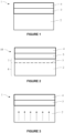
- FD-SOI type substrate represented schematically on the figure 1 under the reference 1, which successively comprises, from its base to its top, a single-crystal semiconductor substrate 2, an electrically insulating layer 3, and a single-crystal semiconductor layer 4.
- the single-crystal substrate 2 is a substrate with high electrical resistivity, and thus has an electrical resistivity of between 500 ⁇ .cm and 30 k ⁇ .cm.
- the single-crystal substrate 2 is a substrate having a high quantity of oxygen, and thus has an interstitial oxygen content (Oi) of between 20 and 40 ppma. Oxygen is trapped in the structure of the monocrystalline substrate, more precisely in the interstices located between the grains of the material constituting the monocrystalline substrate, and is therefore called “interstitial oxygen”.
- the monocrystalline substrate with high electrical resistivity and high quantity of interstitial oxygen is also designated as HR HiOi substrate (combination of the acronyms of the Anglo-Saxon terms “High Resistivity” and “High Oxygen”).
- the single-crystal substrate is made of silicon.
- the single-crystal substrate has P or N type doping.
- the single-crystal substrate 2 is preferably doped with phosphorus, and more preferably, the single-crystal substrate is made of silicon doped with phosphorus.
- the single-crystal substrate 2 is preferably doped with boron, and more preferably, the single-crystal substrate is made of silicon doped with boron.
- the electrically insulating layer 3 comprises a layer of silicon oxide.
- the single crystal layer 3 has P-type doping.
- the single crystal layer is a silicon layer.
- a heat treatment is applied to the FD-SOI type substrate at a temperature greater than or equal to 1175°C, for a time greater than or equal to 1 hour.
- a PN junction, referenced 5, is formed in the monocrystalline substrate 2 at a depth determined with respect to the electrically insulating layer 3, as illustrated in figure 2 .
- heat treatment causes the following phenomena.
- P-type dopants from the single-crystal layer diffuse into the single-crystal substrate through the electrically insulating layer, in a region of the substrate adjacent to the electrically insulating layer.
- the single-crystal substrate is P-type doped
- an inversion of the type of doping occurs in the single-crystal substrate 2.
- the substrate a region 6, called the first region, which extends from the base of the monocrystalline substrate to the P-N junction and which is doped with type N due to the inversion of the type of doping.
- the P-N junction marks the boundary between the first region 6, and the remaining region 7 of the monocrystalline substrate, called the second region, which extends from the P-N junction to the electrically insulating layer 3, and which remains P-type doped. , the diffusion of P-type dopants in this second region having compensated for the inversion of the doping type.
- the single-crystal substrate is N-doped
- the aforementioned phenomenon of diffusion of P-type dopants in the second region occurs.
- the phenomenon of reversal of the type of doping does not occur.
- the first region remains N-type doped.
- the monocrystalline substrate comprises a P-N junction separating the first region (located on the base side of the substrate) doped with type N and the second region ( located on the side of the electrically insulating layer) doped with type P.
- the adjustment of these three characteristics makes it possible to control the formation of the PN junction, and in particular its depth in the monocrystalline substrate 2 from the electrically insulating layer 3.
- the process parameters are adjusted so as to form the P-N junction at a depth of between 1 ⁇ m and 5 ⁇ m from the electrically insulating layer.
- the heat treatment causes the interstitial oxygen present in the monocrystalline substrate 2 to precipitate, which forms thermal donors of the sulfur oxides type S x O y equipped with excess charges coming to dop the material of the monocrystalline substrate, and thus reverse the doping of the latter.
- This first phenomenon is represented schematically on the Figure 3 , on which the doping of the material of the monocrystalline substrate by the thermal donors is represented by the vertical ascending arrows 8.
- the heat treatment causes the diffusion of the dopants of the monocrystalline layer 4, such as boron, through the electrically insulating layer 3 which is sufficiently thin, into the monocrystalline substrate 2.
- dopants can also be used to control the formation of the PN junction, and in particular its depth in the monocrystalline substrate from the electrically insulating layer.
- This second phenomenon is represented schematically on the figure 4 , on which the diffusion of dopants through the electrically insulating layer is represented by the downward vertical arrows 9.
- This second phenomenon combined with the first in the case of a monocrystalline substrate doped with tpe P, leads to the formation of the first region of the N-doping substrate, and to the formation of the second P-doped region, located between the first region and the electrically insulating layer, visible on the semiconductor-on-insulator type structure 10 of the figure 2 .
- the method of the invention offers the advantage of allowing these two phenomena to occur thanks to the three characteristics listed above, without the need for additional processing steps.
- the formation of the P-N junction in the thickness of the substrate in the present invention does not require any localized implantation of dopants or any mask deposition. on the substrate.
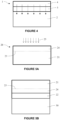
- the FD-SOI type substrate is obtained by transferring a layer of a donor substrate to a recipient substrate.
- a donor substrate 20 comprising a single-crystal layer 21, preferably a silicon layer, having P-type doping, and a weakening zone 23 located in the single-crystal layer delimiting the layer to be transferred 24, as illustrated on there figure 5A .
- the single-crystal layer 24 to be transferred is preferably a silicon layer.
- a monocrystalline receiver substrate 30 is also provided, preferably made of silicon, having an electrical resistivity of between 500 ⁇ .cm and 30 k ⁇ .cm, an interstitial oxygen content (Oi) of between 20 and 40 ppma, and a doping of type P or N.
- the donor substrate 20 is then bonded to the recipient substrate 30 via an electrically insulating layer 22 having a thickness of between 20 nm and 400 nm.
- the electrically insulating layer 22 is then located between the donor substrate 20 and the recipient substrate 30.
- the electrically insulating layer 22 can come from the donor substrate or from the recipient substrate, that is to say it can be initially on the donor substrate or on the recipient substrate before bonding.
- the transfer of layer 24 from the donor substrate 20 to the recipient substrate 30 is carried out in accordance with the Smart Cut TM process, in which the weakened zone 23 is formed by implantation of atomic species, such as for example d atoms. hydrogen and/or helium, in the donor substrate, then the donor substrate is detached along said weakening zone.
- the Smart Cut TM process in which the weakened zone 23 is formed by implantation of atomic species, such as for example d atoms. hydrogen and/or helium, in the donor substrate, then the donor substrate is detached along said weakening zone.
- a donor substrate 20 comprising a single-crystal semiconductor layer 21, preferably a silicon layer, having P-type doping.
- the single crystal layer 21 is preferably a silicon layer.
- a monocrystalline receiver substrate 30 is also provided, preferably made of silicon, having an electrical resistivity of between 500 ⁇ .cm and 30 k ⁇ .cm, an interstitial oxygen content (Oi) of between 20 and 40 ppma, and a doping of type P or N.
- the donor substrate 20 is then bonded to the recipient substrate 30 via an electrically insulating layer 22 having a thickness of between 20 nm and 400 nm.
- the electrically insulating layer 22 is then located between the donor substrate 20 and the recipient substrate 30.
- the electrically insulating layer 22 can come from the donor substrate or from the recipient substrate, that is to say it can be initially on the donor substrate or on the recipient substrate before bonding.
- the donor substrate 20 is then thinned from the surface opposite the recipient substrate to form the transferred layer 24, in order to obtain the substrate 1 of the FD-SOI type.
- FIG. 7 is a graph which illustrates the HD2 gain (dBm) for a semiconductor-on-insulator type structure with or without a PN junction in the high electrical resistivity substrate.
- the HD2 gain corresponds to the second harmonic, measured at a frequency of 900 MHz.
- HD2 is the harmonic generated by the substrate which can interfere with the operation of a radio frequency device comprising the structure according to the invention.
- HD2 is measured across a coplanar line with an entry point and an exit point.
- a power P in (dBm) is imposed, and at the output we measure the power P out which is broken down into several harmonics including in particular HD1 which corresponds to the power measured at the output approximately equal to the power of input, and HD2 which corresponds to the harmonic generated by the substrate.
- the HD2 gain obtained for the structure comprising a PN junction (curve C1) is lower than that obtained for a structure without PN junction (curve C2).
- This downward shift of the C2 curve relative to the C1 curve corresponds to a loss of approximately 10 dBm.
- the high resistivity substrate of the P-N junction structure is more electrically insulating than that of the structure without P-N junction.
- FIG. 8 is a graph which illustrates the S21 gain (dB) for a semiconductor-on-insulator type structure with or without a PN junction, as a function of frequency (Hz).
- the gain S21 corresponds to a measurement of crosstalk or noise (called “cross-talk” in English) which reflects the capacity of components compared to others to communicate through the substrate, thus representing the insulation performance of the substrate.
- FIG. 9 is a graph which illustrates the resistivity R (ohm.cm) of a semiconductor-on-insulator type structure with or without a PN junction in the high electrical resistivity substrate, as a function of frequency (Hz).
- the resistivity obtained for the structure including a PN junction is greater than that obtained for a structure without PN junction (curve C6).
- This downward shift of the C5 curve relative to the C6 curve corresponds to a loss of approximately 1200 ohm.cm.
- the graphs of figures 7, 8 , And 9 thus show that the radio frequency performances of the semiconductor-on-insulator type structure of the invention, comprising a PN junction, are greatly improved compared to those of a structure without a PN junction.
Description
La présente invention concerne un procédé de fabrication d'une structure de type semi-conducteur sur isolant, notamment pour des applications radiofréquences.The present invention relates to a method of manufacturing a semiconductor-on-insulator type structure, in particular for radio frequency applications.
Les structures de type semi-conducteur sur isolant sont des structures multicouches comprenant un substrat qui est généralement en silicium, une couche électriquement isolante agencée sur le substrat, qui est généralement une couche d'oxyde telle qu'une couche d'oxyde de silicium, et une couche semi-conductrice agencée sur la couche isolante, qui est généralement une couche de silicium.Semiconductor-on-insulator type structures are multilayer structures comprising a substrate which is generally made of silicon, an electrically insulating layer arranged on the substrate, which is generally an oxide layer such as a silicon oxide layer, and a semiconductor layer arranged on the insulating layer, which is generally a silicon layer.
De telles structures sont dites structures « Semiconductor on Insulator » (acronyme SeOI) en anglais, en particulier « Silicon on Insulator » (SOI) lorsque le matériau semi-conducteur est du silicium.Such structures are called “Semiconductor on Insulator” (acronym SeOI) structures in English, in particular “Silicon on Insulator” (SOI) when the semiconductor material is silicon.
Parmi les structures SOI existantes, les structures dites « Fully-Depleted Silicon on Insulator» en anglais (acronyme FD-SOI) sont couramment utilisées pour des applications digitales. Les structures FD-SOI se caractérisent par la présence d'une couche mince d'oxyde, agencée sur un substrat support en silicium, et d'une couche semi-conductrice très mince agencée sur la couche d'oxyde, dite couche SOI.Among the existing SOI structures, the so-called “Fully-Depleted Silicon on Insulator” structures (acronym FD-SOI) are commonly used for digital applications. FD-SOI structures are characterized by the presence of a thin oxide layer, arranged on a silicon support substrate, and a very thin semiconductor layer arranged on the oxide layer, called the SOI layer.
La couche d'oxyde se trouve entre le substrat et la couche SOI. La couche d'oxyde est alors dite « enterrée », et est appelée « BOX » pour « Buried OXide » en anglais.The oxide layer is between the substrate and the SOI layer. The oxide layer is then said to be “buried”, and is called “BOX” for “Buried OXide” in English.
La couche SOI permet d'implémenter le canal de conduction de la structure FD-SOI.The SOI layer makes it possible to implement the conduction channel of the FD-SOI structure.
Du fait de la faible épaisseur et de l'uniformité de la couche de BOX et de la couche SOI, il n'est pas nécessaire de doper le canal de conduction, d'où le fait que la structure puisse fonctionner selon un mode totalement déplété.Due to the low thickness and uniformity of the BOX layer and the SOI layer, it is not necessary to dope the conduction channel, hence the fact that the structure can operate in a completely depleted mode. .
Les structures FD-SOI présentent des caractéristiques électrostatiques améliorées par rapport aux structures sans couche de BOX. La couche de BOX diminue la capacité électrique parasite entre la source et le drain, et permet également de réduire considérablement les fuites d'électrons depuis le canal de conduction vers le substrat en confinant le flux d'électrons dans le canal de conduction, réduisant ainsi les pertes de courant électrique et améliorant les performances de la structure.FD-SOI structures exhibit improved electrostatic characteristics compared to structures without a BOX layer. The BOX layer reduces the parasitic electrical capacitance between the source and the drain, and also significantly reduces electron leakage from the conduction channel to the substrate by confining the flow of electrons in the conduction channel, thereby reducing electrical current losses and improving the performance of the structure.
Les structures FD-SOI peuvent être compatibles avec des applications radiofréquences (RF), mais pâtissent cependant de l'apparition de pertes électriques dans ledit substrat.FD-SOI structures can be compatible with radio frequency (RF) applications, but suffer from the appearance of electrical losses in said substrate.
Pour pallier ces pertes électriques et améliorer les performances RF, il est connu d'utiliser un substrat, notamment de type SOI, présentant une haute résistivité électrique, ce type de substrat étant communément appelé « substrat HR » pour substrat à haute résistivité. Ce dernier est avantageusement combiné avec une couche de piégeage de charges (« trap-rich layer » en anglais).To compensate for these electrical losses and improve RF performance, it is known to use a substrate, in particular of the SOI type, having a high electrical resistivity, this type of substrate being commonly called "HR substrate" for high resistivity substrate. The latter is advantageously combined with a charge trapping layer (“trap-rich layer” in English).
Cependant, ce type de substrat n'est pas compatible avec une utilisation de transistors dont la tension de seuil doit être contrôlée par une grille en face arrière (« back bias voltage » en anglais »). En effet, la présence de cette couche comportant des charges piégées gêne la polarisation en face arrière (application d'une différence de potentiel au niveau de la face arrière).However, this type of substrate is not compatible with the use of transistors whose threshold voltage must be controlled by a gate on the rear face ("back bias voltage" in English). Indeed, the presence of this layer comprising trapped charges hinders the polarization on the rear face (application of a potential difference at the level of the rear face).
La publication scientifique "
Par latéralement, on entend que deux régions respectivement dopées P et N sont agencées à une même profondeur du substrat, la jonction entre lesdites régions étant sensiblement perpendiculaire à la surface principale du substrat. Une telle jonction est obtenue par implantation de phosphore sur l'ensemble du substrat pour un dopage de type N suivie d'une implantation localisée de bore au travers d'un masque pour former des régions dopées P, puis d'un traitement thermique d'activation des dopants.By laterally, we mean that two regions respectively doped P and N are arranged at the same depth of the substrate, the junction between said regions being substantially perpendicular to the main surface of the substrate. Such a junction is obtained by implantation of phosphorus on the entire substrate for N-type doping followed by localized implantation of boron through a mask to form P-doped regions, then a heat treatment of activation of dopants.
Alors qu'un semi-conducteur dopé est un bon conducteur, la jonction ne laisse quasiment pas passer le courant électrique, empêchant ainsi la propagation de champs électriques parasites.While a doped semiconductor is a good conductor, the junction allows almost no electric current to pass, thus preventing the propagation of parasitic electric fields.
Un inconvénient résultant d'un agencement latéral de la jonction P-N comme décrit dans la publication scientifique est qu'il nécessite une étape de lithographie pour la formation du masque et deux étapes d'implantation, ce qui représente un surcoût important.A disadvantage resulting from a lateral arrangement of the P-N junction as described in the scientific publication is that it requires a lithography step for the formation of the mask and two implantation steps, which represents a significant additional cost.
Le document
L'article de
Un but de l'invention est de proposer un procédé de fabrication d'une structure de type semi-conducteur sur isolant permettant de surmonter les inconvénients mentionnés précédemment.An aim of the invention is to propose a method of manufacturing a semiconductor-on-insulator type structure making it possible to overcome the drawbacks mentioned above.
L'invention vise à proposer un tel procédé de fabrication permettant de fabriquer une structure de type FD-SOI présentant de bonnes performances radiofréquences.The invention aims to propose such a manufacturing process making it possible to manufacture an FD-SOI type structure having good radio frequency performance.
A cette fin, l'invention propose un procédé de fabrication d'une structure de type semi-conducteur sur isolant, comprenant les étapes suivantes :
- fourniture d'un substrat de type FD-SOI comprenant successivement, depuis sa base vers son sommet :
- un substrat semi-conducteur monocristallin présentant une résistivité électrique comprise entre 500 Ω.cm et 30 kΩ.cm, une teneur en oxygène interstitiel comprise entre 20 et 40 old ppma, et présentant un dopage de type P ou N,
- une couche électriquement isolante présentant une épaisseur comprise entre 20 nm et 400 nm,
- une couche semi-conductrice monocristalline présentant un dopage de type P,
- traitement thermique du substrat de type FD-SOI à une température supérieure ou égale à 1175°C pendant un temps supérieur ou égal à 1h, afin de former une jonction P-N dans le substrat semi-conducteur monocristallin à une profondeur déterminée par rapport à la couche électriquement isolante,
- par la diffusion de dopants de type P depuis la couche semi-conductrice monocristalline au travers de la couche électriquement isolante dans ledit substrat,
- et, si le substrat est dopé de type P, par la formation dans ledit substrat de donneurs thermiques par précipitation de l'oxygène interstitiel, et
- supply of an FD-SOI type substrate comprising successively, from its base to its top:
- a monocrystalline semiconductor substrate having an electrical resistivity of between 500 Ω.cm and 30 kΩ.cm, an interstitial oxygen content of between 20 and 40 ppma, and having P or N type doping,
- an electrically insulating layer having a thickness of between 20 nm and 400 nm,
- a single-crystal semiconductor layer having P-type doping,
- heat treatment of the FD-SOI type substrate at a temperature greater than or equal to 1175°C for a time greater than or equal to 1 hour, in order to form a PN junction in the monocrystalline semiconductor substrate at a depth determined relative to the layer electrically insulating,
- by the diffusion of P-type dopants from the single-crystal semiconductor layer through the electrically insulating layer in said substrate,
- and, if the substrate is P-type doped, by the formation in said substrate of thermal donors by precipitation of interstitial oxygen, and
La principale technique de mesure de l'oxygène interstitiel dans le silicium d'un substrat semi-conducteur est l'absorption infrarouge par spectrométrie infrarouge à transformée de Fourier (acronyme FTIR des termes anglo-saxons Fourier Transform InfraRed spectrometry).The main technique for measuring interstitial oxygen in the silicon of a semiconductor substrate is infrared absorption by Fourier Transform InfraRed Spectrometry (FTIR).
Cette mesure FTIR fournit une valeur d'un coefficient d'absorption αOX dû à l'oxygène interstitiel. La concentration en oxygène interstitiel est calculée à partir de ce coefficient d'absorption αOX, selon la méthode décrite notamment dans le document, «
Selon cette méthode, la concentration en oxygène en atome par cm3 (at/cm3) ou en tant que fraction de la quantité totale d'atomes présents en partie pour million (ppma) est obtenue en multipliant le coefficient d'absorption αOX par un facteur de conversion.According to this method, the oxygen concentration in atoms per cm 3 (at/cm 3 ) or as a fraction of the total quantity of atoms present in parts per million (ppma) is obtained by multiplying the absorption coefficient α OX by a conversion factor.
La concentration en oxygène dont il est question dans l'invention (old ppma) est obtenue en utilisant le premier des quatre facteurs de conversion présentés dans la liste suivante, dit « old ASTM » (acronyme des termes anglo-saxons « American Society for Testing »), exprimé en ppma :
Selon d'autres aspects, le procédé de fabrication de l'invention présente les différentes caractéristiques suivantes prises seules ou selon leurs combinaisons techniquement possibles :
- le substrat monocristallin est en silicium et/ou la couche monocristalline est une couche de silicium ;
- le substrat de type FD-SOI est obtenu par transfert d'une couche d'un substrat donneur sur un substrat receveur, selon les étapes suivantes :
- fourniture
- du substrat donneur comprenant une couche semi-conductrice monocristalline présentant un dopage de type P, et une zone de fragilisation située dans la couche de silicium monocristallin délimitant la couche à transférer, et
- du substrat receveur semi-conducteur monocristallin, présentant une résistivité électrique comprise entre 500 Ω.cm et 30 kΩ.cm, une teneur en oxygène interstitiel comprise entre 20 et 40 old ppma, et un dopage de type P ou N,
- collage du substrat donneur sur le substrat receveur par l'intermédiaire d'une couche électriquement isolante présentant une épaisseur comprise entre 20 nm et 400 nm,
- détachement du substrat donneur le long de la zone de fragilisation, pour former le substrat de type FD-SOI ;
- fourniture
- le substrat de type FD-SOI est obtenu par transfert d'une couche d'un substrat donneur sur un substrat receveur, selon les étapes suivantes :
- fourniture
- du substrat donneur comprenant une couche semi-conductrice monocristalline présentant un dopage de type P, et
- du substrat receveur semi-conducteur monocristallin, présentant une résistivité électrique comprise entre 500 Ω.cm et 30 kΩ.cm, une teneur en oxygène interstitiel comprise entre 20 et 40 old ppma, et un dopage de type P ou N,
- collage du substrat donneur sur le substrat receveur par l'intermédiaire d'une couche électriquement isolante présentant une épaisseur comprise entre 20 et 400nm,
- amincissement du substrat donneur depuis la surface opposée au substrat receveur pour former la couche transférée, afin d'obtenir le substrat de type FD-SOI ;
- fourniture
- la zone de fragilisation est formée par implantation d'espèces atomiques dans le substrat donneur, afin de délimiter la couche à transférer ;
- le substrat receveur et la couche monocristalline du substrat donneur sont dopés P avec du bore ;
- la jonction P-N est formée à une profondeur comprise entre 1 µm et 5 µm à partir de la couche électriquement isolante ;
- la couche électriquement isolante comprend une couche d'oxyde de silicium.
- the single-crystal substrate is made of silicon and/or the single-crystal layer is a layer of silicon;
- the FD-SOI type substrate is obtained by transferring a layer of a donor substrate to a recipient substrate, according to the following steps:
- supply
- of the donor substrate comprising a single-crystal semiconductor layer having P-type doping, and a weakening zone located in the single-crystal silicon layer delimiting the layer to be transferred, and
- of the monocrystalline semiconductor receiver substrate, having an electrical resistivity of between 500 Ω.cm and 30 kΩ.cm, an interstitial oxygen content of between 20 and 40 ppma, and a P or N type doping,
- bonding the donor substrate to the recipient substrate via an electrically insulating layer having a thickness of between 20 nm and 400 nm,
- detachment of the donor substrate along the weakening zone, to form the FD-SOI type substrate;
- supply
- the FD-SOI type substrate is obtained by transferring a layer of a donor substrate to a recipient substrate, according to the following steps:
- supply
- of the donor substrate comprising a single-crystal semiconductor layer having P-type doping, and
- of the monocrystalline semiconductor receiver substrate, having an electrical resistivity of between 500 Ω.cm and 30 kΩ.cm, a content of interstitial oxygen between 20 and 40 ppma, and P or N type doping,
- bonding the donor substrate to the recipient substrate via an electrically insulating layer having a thickness of between 20 and 400nm,
- thinning of the donor substrate from the surface opposite the recipient substrate to form the transferred layer, in order to obtain the FD-SOI type substrate;
- supply
- the weakening zone is formed by implantation of atomic species in the donor substrate, in order to delimit the layer to be transferred;
- the recipient substrate and the single crystal layer of the donor substrate are P doped with boron;
- the PN junction is formed at a depth of between 1 µm and 5 µm from the electrically insulating layer;
- the electrically insulating layer comprises a layer of silicon oxide.
Un autre aspect, qui ne fait pas l'objet des revendications, concerne une structure de type semi-conducteur sur isolant obtenue directement par la mise en oeuvre du procédé de fabrication décrit précédemment, ladite structure de type semi-conducteur sur isolant comprenant successivement, depuis sa base vers son sommet :
- un substrat semi-conducteur monocristallin présentant une résistivité électrique comprise entre 500 Ω.cm et 30 kΩ.cm, une teneur en oxygène interstitiel comprise entre 20 et 40 old ppma, et comprenant :
- une première région comprenant un dopage de type N,
- une deuxième région agencée sur la première région, comprenant un dopage de type P, la deuxième région étant séparée de la première région par une jonction P-N,
- une couche électriquement isolante,
- une couche semi-conductrice monocristalline comprenant un dopage de type P.
- a monocrystalline semiconductor substrate having an electrical resistivity of between 500 Ω.cm and 30 kΩ.cm, an interstitial oxygen content of between 20 and 40 ppma, and comprising:
- a first region comprising N-type doping,
- a second region arranged on the first region, comprising P-type doping, the second region being separated from the first region by a PN junction,
- an electrically insulating layer,
- a single-crystal semiconductor layer comprising P-type doping.
Selon d'autres aspects, ladite structure présente les différentes caractéristiques suivantes prises seules ou selon leurs combinaisons techniquement possibles :
- la couche semi-conductrice monocristalline est dopée P avec du bore ;
- la jonction P-N est située à une profondeur comprise entre 1 µm et 5 µm à partir de la couche électriquement isolante ;
- la couche électriquement isolante comprend une couche d'oxyde de silicium ;
- le substrat monocristallin est en silicium et/ou la couche monocristalline est une couche de silicium.
- the single-crystal semiconductor layer is P-doped with boron;
- the PN junction is located at a depth of between 1 µm and 5 µm from the electrically insulating layer;
- the electrically insulating layer comprises a layer of silicon oxide;
- the single-crystal substrate is made of silicon and/or the single-crystal layer is a layer of silicon.
D'autres avantages et caractéristiques de l'invention apparaîtront à la lecture de la description suivante donnée à titre d'exemple illustratif et non limitatif, en référence aux figures annexées suivantes :
- la
figure 1 est un schéma d'un substrat de type FD-SOI ; - la
figure 2 est un schéma d'une structure de type semi-conducteur sur isolant comprenant une jonction P-N, conformément à l'invention ; - la
figure 3 est un schéma qui illustre l'inversion du dopage d'une portion du substrat monocristallin à haute résistivité électrique ; - la
figure 4 est un schéma qui illustre la diffusion du dopant de la couche monocristalline au travers de la couche électriquement isolante sous-jacente ; - la
figure 5A est un schéma qui illustre la formation d'une zone de fragilisation par implantation d'espèces atomiques dans un substrat donneur, selon un premier mode de réalisation ; - la
figure 5B est un schéma qui illustre le collage du substrat donneur sur un substrat receveur selon le premier mode de réalisation ; - la
figure 5C est un schéma qui illustre le décollement du substrat donneur le long de la zone de fragilisation, et le transfert d'une couche depuis le substrat donneur sur le substrat receveur, selon le premier mode de réalisation ; - la
figure 6A est un schéma qui illustre le collage du substrat donneur sur un substrat receveur selon un deuxième mode de réalisation ; - la
figure 6B est un schéma qui illustre l'amincissement du substrat donneur depuis la surface opposée au substrat receveur pour former la couche transférée ; - la
figure 7 est un graphe qui illustre le gain HD2 pour une structure de type semi-conducteur sur isolant avec ou sans jonction P-N dans le substrat à haute résistivité électrique, - la
figure 8 est un graphe qui illustre le gain S21 pour une structure de type semi-conducteur sur isolant avec ou sans jonction P-N dans le substrat à haute résistivité électrique ; - la
figure 9 est un graphe qui illustre la résistivité d'une structure de type semi-conducteur sur isolant avec ou sans jonction P-N dans le substrat à haute résistivité électrique.
- there
figure 1 is a diagram of an FD-SOI type substrate; - there
figure 2 is a diagram of a semiconductor-on-insulator type structure comprising a PN junction, in accordance with the invention; - there
Figure 3 is a diagram which illustrates the inversion of the doping of a portion of the monocrystalline substrate with high electrical resistivity; - there
figure 4 is a diagram which illustrates the diffusion of the dopant from the single crystal layer through the underlying electrically insulating layer; - there
figure 5A is a diagram which illustrates the formation of a weakening zone by implantation of atomic species in a donor substrate, according to a first embodiment; - there
Figure 5B is a diagram which illustrates the bonding of the donor substrate to a recipient substrate according to the first embodiment; - there
Figure 5C is a diagram which illustrates the separation of the donor substrate along the weakened zone, and the transfer of a layer from the donor substrate to the recipient substrate, according to the first embodiment; - there
Figure 6A is a diagram which illustrates the bonding of the donor substrate to a recipient substrate according to a second embodiment; - there
Figure 6B is a diagram which illustrates the thinning of the donor substrate from the surface opposite the recipient substrate to form the transferred layer; - there
Figure 7 is a graph which illustrates the HD2 gain for a semiconductor-on-insulator type structure with or without a PN junction in the high electrical resistivity substrate, - there
figure 8 is a graph which illustrates the gain S21 for a semiconductor-on-insulator type structure with or without a PN junction in the high electrical resistivity substrate; - there
Figure 9 is a graph that illustrates the resistivity of a semiconductor-on-insulator type structure with or without a PN junction in the high electrical resistivity substrate.
L'invention concerne un procédé de fabrication d'une structure de type semi-conducteur sur isolant, ainsi qu'une telle structure.The invention relates to a method for manufacturing a semiconductor-on-insulator type structure, as well as such a structure.
Le procédé de fabrication de l'invention permet de fabriquer des structures de type semi-conducteur sur isolant comprenant une jonction P-N conférant à ladite structure de bonnes propriétés radiofréquences, et ce de manière simple et peu coûteuse.The manufacturing method of the invention makes it possible to manufacture semiconductor-on-insulator type structures comprising a P-N junction giving said structure good radio frequency properties, in a simple and inexpensive manner.
On fournit initialement un substrat de type FD-SOI, représenté schématiquement sur la
Le substrat monocristallin 2 est un substrat à haute résistivité électrique, et présente ainsi une résistivité électrique comprise entre 500 Ω.cm et 30 kΩ.cm.The single-
De plus, le substrat monocristallin 2 est un substrat présentant une quantité élevée en oxygène, et présente ainsi une teneur en oxygène interstitiel (Oi) comprise entre 20 et 40 old ppma. L'oxygène est emprisonné dans la structure du substrat monocristallin, plus précisément dans les interstices situés entre les grains du matériau constitutif du substrat monocristallin, et est donc appelé « oxygène interstitiel ».In addition, the single-
Le substrat monocristallin à haute résistivité électrique et quantité élevée en oxygène interstitiel est également désigné en tant que substrat HR HiOi (réunion des acronymes des termes anglo-saxons « High Resistivity » et « High Oxygen »).The monocrystalline substrate with high electrical resistivity and high quantity of interstitial oxygen is also designated as HR HiOi substrate (combination of the acronyms of the Anglo-Saxon terms “High Resistivity” and “High Oxygen”).
De préférence, le substrat monocristallin est en silicium.Preferably, the single-crystal substrate is made of silicon.
Le substrat monocristallin présente un dopage de type P ou N.The single-crystal substrate has P or N type doping.
Dans le cas d'un dopage de type N, le substrat monocristallin 2 est de préférence dopé par du phosphore, et de manière davantage préférée, le substrat monocristallin est en silicium dopé par du phosphore.In the case of N-type doping, the single-
Dans le cas d'un dopage de type P, le substrat monocristallin 2 est de préférence dopé par du bore, et de manière davantage préférée, le substrat monocristallin est en silicium dopé par du bore.In the case of P-type doping, the single-
La couche électriquement isolante 3, également désignée en tant que couche BOX, en ce qu'elle est agencée entre le substrat monocristallin 2 sous-jacent et la couche monocristalline 4 sus-jacente, présente une épaisseur comprise entre 20 nm et 400 nm.The electrically insulating
De préférence, la couche électriquement isolante 3 comprend une couche d'oxyde de silicium.Preferably, the electrically insulating
La couche monocristalline 3 présente un dopage de type P.The
De préférence, la couche monocristalline est une couche de silicium.Preferably, the single crystal layer is a silicon layer.
Selon le procédé de l'invention, on applique un traitement thermique au substrat de type FD-SOI à une température supérieure ou égale à 1175°C, pendant un temps supérieur ou égal à 1h.According to the method of the invention, a heat treatment is applied to the FD-SOI type substrate at a temperature greater than or equal to 1175°C, for a time greater than or equal to 1 hour.
Pendant ledit traitement thermique, il se forme une jonction P-N, référencée 5, dans le substrat monocristallin 2 à une profondeur déterminée par rapport à la couche électriquement isolante 3, comme l'illustre la
Plus précisément, le traitement thermique provoque les phénomènes suivants.More specifically, heat treatment causes the following phenomena.
D'une part, des dopants de type P de la couche monocristalline diffusent dans le substrat monocristallin au travers de la couche électriquement isolante, dans une région du substrat voisine de la couche électriquement isolante.On the one hand, P-type dopants from the single-crystal layer diffuse into the single-crystal substrate through the electrically insulating layer, in a region of the substrate adjacent to the electrically insulating layer.
D'autre part, lorsque le substrat monocristallin est dopé de type P, il se produit une inversion du type de dopage dans le substrat monocristallin 2.On the other hand, when the single-crystal substrate is P-type doped, an inversion of the type of doping occurs in the single-
La combinaison de ces deux phénomènes produit dans le substrat une région 6, dite première région, qui s'étend depuis la base du substrat monocristallin jusqu'à la jonction P-N et qui est dopée de type N du fait de l'inversion du type de dopage. La jonction P-N marque alors la frontière entre la première région 6, et la région restante 7 du substrat monocristallin, dite deuxième région, qui s'étend depuis la jonction P-N jusqu'à la couche électriquement isolante 3, et qui reste dopée de type P, la diffusion des dopants de type P dans cette deuxième région ayant compensé l'inversion du type de dopage.The combination of these two phenomena produces in the substrate a
Lorsque le substrat monocristallin est dopé N, le phénomène susmentionné de diffusion des dopants de type P dans la deuxième région se produit. En revanche, le phénomène d'inversion du type de dopage ne se produit pas. En conséquence, la première région reste dopée de type N.When the single-crystal substrate is N-doped, the aforementioned phenomenon of diffusion of P-type dopants in the second region occurs. On the other hand, the phenomenon of reversal of the type of doping does not occur. As a result, the first region remains N-type doped.
Quel que soit le type de dopage initial du substrat monocristallin, à l'issue du traitement thermique, le substrat monocristallin comprend une jonction P-N séparant la première région (située du côté de la base du substrat) dopée de type N et la deuxième région (située du côté de la couche électriquement isolante) dopée de type P.Whatever the type of initial doping of the monocrystalline substrate, at the end of the heat treatment, the monocrystalline substrate comprises a P-N junction separating the first region (located on the base side of the substrate) doped with type N and the second region ( located on the side of the electrically insulating layer) doped with type P.
La formation de la jonction P-N est rendue possible par les trois caractéristiques suivantes :
- le dopage P de la couche monocristalline 4,
- la température du traitement thermique supérieure ou égale à 1175°C, pendant un temps supérieur ou égal à 1 heure,
- et, dans le cas d'un substrat monocristallin dopé de type P, la concentration élevée en oxygène interstitiel dudit substrat monocristallin 2.
- the P doping of the
monocrystalline layer 4, - the heat treatment temperature greater than or equal to 1175°C, for a time greater than or equal to 1 hour,
- and, in the case of a P-type doped single-crystal substrate, the high interstitial oxygen concentration of said single-
crystal substrate 2.
La présence de la jonction P-N associée à la haute résistivité électrique du substrat cristallin 2, comprise entre 500 Ω.cm et 30 kΩ.cm, permet d'obtenir une structure présentant de très bonnes propriétés radiofréquences. Ces propriétés seront illustrées dans la suite du présent texte. L'ajustement de ces trois caractéristiques permet de contrôler la formation de la jonction P-N, et en particulier sa profondeur dans le substrat monocristallin 2 depuis la couche électriquement isolante 3.The presence of the PN junction associated with the high electrical resistivity of the
Les paramètres du procédé, tels que par exemple les trois caractéristiques mentionnées précédemment, sont ajustés de manière à former la jonction P-N à une profondeur comprise entre 1 µm et 5 µm à partir de la couche électriquement isolante.The process parameters, such as for example the three characteristics mentioned above, are adjusted so as to form the P-N junction at a depth of between 1 µm and 5 µm from the electrically insulating layer.
Dans le cas d'un substrat monocristallin de type P, le traitement thermique fait précipiter l'oxygène interstitiel présent dans le substrat monocristallin 2, ce qui forme des donneurs thermiques de type oxydes de soufre SxOy dotés de charges excédentaires venant doper le matériau du substrat monocristallin, et ainsi inverser le dopage de ce dernier. Ce premier phénomène est représenté schématiquement sur la
Par ailleurs, que le substrat monocristallin soit dopé de type N ou P, le traitement thermique provoque la diffusion des dopants de la couche monocristalline 4, tels que le bore, au travers de la couche électriquement isolante 3 qui est suffisamment fine, jusque dans le substrat monocristallin 2. Ces dopants peuvent également être utilisés pour contrôler la formation de la jonction P-N, et en particulier sa profondeur dans le substrat monocristallin depuis la couche électriquement isolante. Ce deuxième phénomène est représenté schématiquement sur la
Ce deuxième phénomène, combiné au premier dans le cas d'un substrat monocristallin dopé de tpe P, conduisent à la formation de la première région du substrat de dopage N, et à la formation de la deuxième région dopée P, située entre la première région et la couche électriquement isolante, visibles sur la structure 10 de type semi-conducteur sur isolant de la
Le procédé de l'invention offre l'avantage de permettre à ces deux phénomènes de se produire grâce aux trois caractéristiques listées précédemment, sans nécessité d'étapes de traitement supplémentaires. En particulier, contrairement à la jonction P-N latérale décrite dans l'article de M. Rack et al précité, la formation de la jonction P-N dans l'épaisseur du substrat dans la présente invention ne nécessite aucune implantation localisée de dopants ni aucun dépôt de masque sur le substrat.The method of the invention offers the advantage of allowing these two phenomena to occur thanks to the three characteristics listed above, without the need for additional processing steps. In particular, unlike the lateral P-N junction described in the aforementioned article by M. Rack et al, the formation of the P-N junction in the thickness of the substrate in the present invention does not require any localized implantation of dopants or any mask deposition. on the substrate.
Selon un mode de réalisation préféré, le substrat de type FD-SOI est obtenu par transfert d'une couche d'un substrat donneur sur un substrat receveur.According to a preferred embodiment, the FD-SOI type substrate is obtained by transferring a layer of a donor substrate to a recipient substrate.
Selon une première alternative de ce mode de réalisation illustré sur les
La couche monocristalline 24 à transférer est de préférence une couche de silicium.The single-
On fournit également un substrat receveur monocristallin 30, de préférence en silicium, présentant une résistivité électrique comprise entre 500 Ω.cm et 30 kΩ.cm, une teneur en oxygène interstitiel (Oi) comprise entre 20 et 40 old ppma, et un dopage de type P ou N.A
En référence à la
La couche électriquement isolante 22 peut provenir du substrat donneur ou du substrat receveur, c'est-à-dire qu'elle peut se trouver initialement sur le substrat donneur ou sur le substrat receveur avant collage.The electrically insulating
En référence à la
De préférence, le transfert de la couche 24 du substrat donneur 20 vers le substrat receveur 30 est réalisée conformément au procédé Smart Cut™, dans lequel la zone de fragilisation 23 est formée par implantation d'espèces atomiques, telles que par exemple des atomes d'hydrogène et/ou d'hélium, dans le substrat donneur, puis le substrat donneur est détaché le long de ladite zone de fragilisation.Preferably, the transfer of
Selon une deuxième alternative de ce mode de réalisation illustré sur les
La couche monocristalline 21 est de préférence une couche de silicium.The
On fournit également un substrat receveur monocristallin 30, de préférence en silicium, présentant une résistivité électrique comprise entre 500 Ω.cm et 30 kΩ.cm, une teneur en oxygène interstitiel (Oi) comprise entre 20 et 40 old ppma, et un dopage de type P ou N.A
En référence à la
La couche électriquement isolante 22 peut provenir du substrat donneur ou du substrat receveur, c'est-à-dire qu'elle peut se trouver initialement sur le substrat donneur ou sur le substrat receveur avant collage.The electrically insulating
En référence à la
Les bonnes propriétés radiofréquences de la structure de type semi-conducteur sur isolant obtenue par le procédé décrit précédemment sont illustrées à l'aides des
La
Le gain HD2 correspond au second harmonique, mesuré à une fréquence de 900 Mhz.The HD2 gain corresponds to the second harmonic, measured at a frequency of 900 MHz.
Plus précisément, HD2 est l'harmonique généré par le substrat pouvant parasiter le fonctionnement d'un dispositif radiofréquence comprenant la structure selon l'invention. Plus le HD2 est faible, plus le substrat est isolant. Le HD2 est mesuré à travers une ligne coplanaire avec un point d'entrée et un point de sortie. Au point d'entrée, on impose une puissance Pin (dBm), et en sortie on mesure la puissance Pout qui se décompose en plusieurs harmoniques dont en particulier HD1 qui correspond à la puissance mesurée en sortie approximativement égale à la puissance d'entrée, et HD2 qui correspond à l'harmonique généré par le substrat.More precisely, HD2 is the harmonic generated by the substrate which can interfere with the operation of a radio frequency device comprising the structure according to the invention. The lower the HD2, the more insulating the substrate. HD2 is measured across a coplanar line with an entry point and an exit point. At the entry point, a power P in (dBm) is imposed, and at the output we measure the power P out which is broken down into several harmonics including in particular HD1 which corresponds to the power measured at the output approximately equal to the power of input, and HD2 which corresponds to the harmonic generated by the substrate.
D'après le graphe de la
Dès lors, le substrat à haute résistivité de la structure à jonction P-N est plus isolant électriquement que celui de la structure sans jonction P-N.Therefore, the high resistivity substrate of the P-N junction structure is more electrically insulating than that of the structure without P-N junction.
La
Le gain S21 correspond à une mesure de diaphonie ou bruit (appelé « cross-talk » en anglo-saxon) qui traduit la capacité de composants par rapport à d'autres de communiquer à travers le substrat, représentant ainsi la performance d'isolation du substrat.The gain S21 corresponds to a measurement of crosstalk or noise (called “cross-talk” in English) which reflects the capacity of components compared to others to communicate through the substrate, thus representing the insulation performance of the substrate.
D'après le graphe de la
La
D'après le graphe de la
Ceci confirme le fait que le substrat à haute résistivité de la structure à jonction P-N est plus isolant électriquement que celui de la structure sans jonction P-N.This confirms the fact that the high resistivity substrate of the P-N junction structure is more electrically insulating than that of the structure without P-N junction.
Les graphes des
Claims (8)
- Process for manufacturing a semiconductor-on-insulator structure (10), comprising the following steps:- provision of an FD-SOI substrate (1) comprising successively, from its base to its top:• a single-crystal semiconductor substrate (2) with an electrical resistivity of between 500 Ω.cm and 30 kΩ.cm, an interstitial oxygen (Oi) content of between 20 and 40 old ppma, and doping of a first P or N type,• an electrically insulating layer (3) with a thickness of between 20 nm and 400 nm, and• a single-crystal semiconductor layer (4) with P-type doping,- heat treatment of the FD-SOI substrate (1) at a temperature greater than or equal to 1175°C for a time greater than or equal to 1h, in order to form a P-N junction (5) in the single-crystal semiconductor substrate (2) at a determined depth with respect to the electrically insulating layer (3),so as to form, in the substrate, a first region (6) with N-type doping extending between the base of the substrate and the P-N junction and a second P-doped region (7) located between the first region (6) and the electrically insulating layer (3).• by diffusion of P-type dopants from the single-crystal semiconductor layer (4) through the electrically insulating layer (3) in said substrate (2),• and, if the substrate (2) has P-type doping, by the formation in said substrate (2) of thermal donors by precipitation of interstitial oxygen,
- Manufacturing process according to claim 1, wherein the single-crystal substrate (2) is made of silicon and/or the single-crystal layer (4) is a silicon layer.
- Manufacturing process according to claim 1 or claim 2, wherein the FD-SOI substrate (1) is obtained by transferring a layer (24) of a donor substrate (20) onto a receiver substrate (30), according to the following steps:- provision of• the donor substrate (20) comprising a single-crystal semiconductor layer (21) with P-type doping, and an embrittlement zone (23) located in the single-crystal silicon layer (21) delimiting the layer to be transferred (24), and• the single-crystal semiconductor receiver substrate (30), having an electrical resistivity of between 500 Ω.cm and 30 kΩ.cm, an interstitial oxygen (Oi) content of between 20 and 40 old ppma, and a doping of a first P or N type,- bonding of the donor substrate (20) to the receiver substrate (30) via an electrically insulating layer (22) with a thickness of between 20 nm and 400 nm,- detachment of the donor substrate (20) along the embrittlement zone (23), to form the FD-SOI substrate (1).
- Manufacturing process according to claim 1 or claim 2, wherein the FD-SOI substrate (1) is obtained by transferring a layer (24) of a donor substrate (20) onto a receiver substrate (30), according to the following steps:- provision of:• a donor substrate (20) comprising a single-crystal semiconductor layer (21) with P-type doping, and• the single-crystal semiconductor receiver substrate (30), with an electrical resistivity of between 500 Ω.cm and 30 kΩ.cm, an interstitial oxygen (Oi) content of between 20 and 40 old ppma, and P- or N-type doping,- bonding of the donor substrate (20) to the receiver substrate (30) via an electrically insulating layer (22) with a thickness of between 20 and 400 nm,- thinning of the donor substrate (20) from the surface opposite the receiver substrate (30) to form the transferred layer (24), to obtain the FD-SOI substrate (1).
- Process according to claim 3, wherein the embrittlement zone (24) is formed by implanting atomic species into the donor substrate (20), in order to delimit the layer to be transferred (24).
- Process according to any one of claims 3 to 5, wherein the receiver substrate (30) and the single-crystal layer (21) of the donor substrate are P-doped with boron.
- A process according to any of the preceding claims, wherein the P-N junction (5) is formed at a depth of between 1 µm and 5 µm from the electrically insulating layer (3).
- A process according to any of the preceding claims, wherein the electrically insulating layer (3) comprises a silicon oxide layer.
Applications Claiming Priority (2)
| Application Number | Priority Date | Filing Date | Title |
|---|---|---|---|
| FR2000098A FR3106019B1 (en) | 2020-01-07 | 2020-01-07 | MANUFACTURING PROCESS OF A SEMICONDUCTOR TYPE STRUCTURE ON INSULATION FOR RADIO FREQUENCY APPLICATIONS |
| PCT/FR2021/050018 WO2021140300A1 (en) | 2020-01-07 | 2021-01-07 | Method for manufacturing a semiconductor-on-insulator structure for radiofrequency applications |
Publications (2)
| Publication Number | Publication Date |
|---|---|
| EP4088312A1 EP4088312A1 (en) | 2022-11-16 |
| EP4088312B1 true EP4088312B1 (en) | 2024-03-13 |
Family
ID=70154624
Family Applications (1)
| Application Number | Title | Priority Date | Filing Date |
|---|---|---|---|
| EP21704847.9A Active EP4088312B1 (en) | 2020-01-07 | 2021-01-07 | Method for manufacturing a semiconductor-on-insulator structure for radiofrequency applications |
Country Status (7)
| Country | Link |
|---|---|
| US (1) | US20230025429A1 (en) |
| EP (1) | EP4088312B1 (en) |
| JP (1) | JP2023509380A (en) |
| KR (1) | KR20220123671A (en) |
| CN (1) | CN114930516A (en) |
| FR (1) | FR3106019B1 (en) |
| WO (1) | WO2021140300A1 (en) |
Families Citing this family (1)
| Publication number | Priority date | Publication date | Assignee | Title |
|---|---|---|---|---|
| FR3133481A1 (en) * | 2022-03-11 | 2023-09-15 | Soitec | Process for manufacturing a multilayer structure of the semiconductor type on insulator |
Family Cites Families (1)
| Publication number | Priority date | Publication date | Assignee | Title |
|---|---|---|---|---|
| CN103430298B (en) * | 2011-03-16 | 2016-03-16 | Memc电子材料有限公司 | There is the silicon on insulated substrate of high resistivity portion and manufacture the method for this class formation in process wafer |
-
2020
- 2020-01-07 FR FR2000098A patent/FR3106019B1/en active Active
-
2021
- 2021-01-07 KR KR1020227025992A patent/KR20220123671A/en active Search and Examination
- 2021-01-07 CN CN202180008062.5A patent/CN114930516A/en active Pending
- 2021-01-07 EP EP21704847.9A patent/EP4088312B1/en active Active
- 2021-01-07 US US17/757,822 patent/US20230025429A1/en active Pending
- 2021-01-07 JP JP2022538205A patent/JP2023509380A/en active Pending
- 2021-01-07 WO PCT/FR2021/050018 patent/WO2021140300A1/en unknown
Also Published As
| Publication number | Publication date |
|---|---|
| CN114930516A (en) | 2022-08-19 |
| FR3106019A1 (en) | 2021-07-09 |
| JP2023509380A (en) | 2023-03-08 |
| FR3106019B1 (en) | 2021-12-10 |
| US20230025429A1 (en) | 2023-01-26 |
| KR20220123671A (en) | 2022-09-08 |
| WO2021140300A1 (en) | 2021-07-15 |
| EP4088312A1 (en) | 2022-11-16 |
Similar Documents
| Publication | Publication Date | Title |
|---|---|---|
| EP2279520B1 (en) | Method for making complementary p and n mosfet transistors | |
| FR2616590A1 (en) | METHOD FOR MANUFACTURING AN INSULATED LAYER BOUND IN A SEMICONDUCTOR SUBSTRATE BY IONAL IMPLANTATION AND SEMICONDUCTOR STRUCTURE COMPRISING SAID LAYER | |
| EP1949430A1 (en) | Treating a germanium layer bonded to a substrate | |
| FR2972567A1 (en) | METHOD OF FORMING A STRUCTURE OF GE ON III / V ON INSULATION | |
| FR2795554A1 (en) | Making silicon-on-nothing architecture for high-speed CMOS signal- and low voltage power devices, includes formation of internal passivated or insulated cavities in stacked semiconductor assemblies | |
| FR3051596A1 (en) | METHOD FOR MANUFACTURING A CONDUCTIVE SEMICONDUCTOR TYPE SUBSTRATE ON INSULATION | |
| EP3531444A1 (en) | Integrated circuit including a substrate provided with a region rich in traps, and method for manufacturing same | |
| EP3127142A1 (en) | Method for manufacture of a semiconductor wafer suitable for the manufacture of an soi substrate, and soi substrate wafer thus obtained | |
| FR3051595A1 (en) | METHOD FOR MANUFACTURING A CONDUCTIVE SEMICONDUCTOR TYPE SUBSTRATE ON INSULATION | |
| EP4088312B1 (en) | Method for manufacturing a semiconductor-on-insulator structure for radiofrequency applications | |
| EP0797252B1 (en) | Silicon on insulator substrate for fabricating transistors and method for preparing such a substrate | |
| FR2693314A1 (en) | Vertical JFET transistor with optimized bipolar operating mode and corresponding manufacturing process. | |
| WO2020136343A1 (en) | Semiconductor structure for digital and radiofrequency applications | |
| EP3903342B1 (en) | Semiconductor structure for digital and radiofrequency applications, and method for manufacturing such a structure | |
| FR3118828A1 (en) | Process for direct bonding of substrates | |
| EP3903341B1 (en) | Method for manufacturing a substrate for a front-facing image sensor | |
| EP3826061B1 (en) | Hybrid electronic device and method for manufacturing such a device | |
| FR3076397A1 (en) | PROCESS FOR PRODUCING A TRANSISTOR | |
| WO2022195226A1 (en) | Ncfet transistor comprising a semiconductor-on-insulator substrate | |
| WO2021234277A1 (en) | Method for manufacturing a semiconductor-on-insulator substrate for radiofrequency applications | |
| FR3027451A1 (en) | SUBSTRATE AND METHOD FOR MANUFACTURING SUBSTRATE | |
| FR3136109A1 (en) | Silicon-on-insulator type semiconductor device and corresponding manufacturing method | |
| FR3109017A1 (en) | MANUFACTURING PROCESS OF AN INTEGRATED CIRCUIT CHIP on SeOI | |
| FR2693313A1 (en) | Vertical JFET transistor with reduced grid / substrate capacity, and corresponding manufacturing process. |
Legal Events
| Date | Code | Title | Description |
|---|---|---|---|
| STAA | Information on the status of an ep patent application or granted ep patent |
Free format text: STATUS: UNKNOWN |
|
| STAA | Information on the status of an ep patent application or granted ep patent |
Free format text: STATUS: THE INTERNATIONAL PUBLICATION HAS BEEN MADE |
|
| PUAI | Public reference made under article 153(3) epc to a published international application that has entered the european phase |
Free format text: ORIGINAL CODE: 0009012 |
|
| STAA | Information on the status of an ep patent application or granted ep patent |
Free format text: STATUS: REQUEST FOR EXAMINATION WAS MADE |
|
| 17P | Request for examination filed |
Effective date: 20220722 |
|
| AK | Designated contracting states |
Kind code of ref document: A1 Designated state(s): AL AT BE BG CH CY CZ DE DK EE ES FI FR GB GR HR HU IE IS IT LI LT LU LV MC MK MT NL NO PL PT RO RS SE SI SK SM TR |
|
| DAV | Request for validation of the european patent (deleted) | ||
| DAX | Request for extension of the european patent (deleted) | ||
| STAA | Information on the status of an ep patent application or granted ep patent |
Free format text: STATUS: EXAMINATION IS IN PROGRESS |
|
| 17Q | First examination report despatched |
Effective date: 20230629 |
|
| REG | Reference to a national code |
Ref country code: DE Ref legal event code: R079 Ref document number: 602021010401 Country of ref document: DE Free format text: PREVIOUS MAIN CLASS: H01L0021761000 Ipc: H01L0021324000 Ref country code: DE Ref legal event code: R079 Free format text: PREVIOUS MAIN CLASS: H01L0021761000 Ipc: H01L0021324000 |
|
| GRAP | Despatch of communication of intention to grant a patent |
Free format text: ORIGINAL CODE: EPIDOSNIGR1 |
|
| STAA | Information on the status of an ep patent application or granted ep patent |
Free format text: STATUS: GRANT OF PATENT IS INTENDED |
|
| RIC1 | Information provided on ipc code assigned before grant |
Ipc: H01L 21/761 20060101ALI20231121BHEP Ipc: H01L 21/02 20060101ALI20231121BHEP Ipc: H01L 21/762 20060101ALI20231121BHEP Ipc: H01L 21/225 20060101ALI20231121BHEP Ipc: H01L 21/324 20060101AFI20231121BHEP |
|
| INTG | Intention to grant announced |
Effective date: 20231207 |
|
| GRAS | Grant fee paid |
Free format text: ORIGINAL CODE: EPIDOSNIGR3 |
|
| GRAA | (expected) grant |
Free format text: ORIGINAL CODE: 0009210 |
|
| STAA | Information on the status of an ep patent application or granted ep patent |
Free format text: STATUS: THE PATENT HAS BEEN GRANTED |
|
| AK | Designated contracting states |
Kind code of ref document: B1 Designated state(s): AL AT BE BG CH CY CZ DE DK EE ES FI FR GB GR HR HU IE IS IT LI LT LU LV MC MK MT NL NO PL PT RO RS SE SI SK SM TR |
|
| REG | Reference to a national code |
Ref country code: GB Ref legal event code: FG4D Free format text: NOT ENGLISH |
|
| REG | Reference to a national code |
Ref country code: CH Ref legal event code: EP |
|
| REG | Reference to a national code |
Ref country code: DE Ref legal event code: R096 Ref document number: 602021010401 Country of ref document: DE |