EP4285392B1 - Übertragung von nanostrukturen unter verwendung von vernetzbaren copolymerfolien - Google Patents
Übertragung von nanostrukturen unter verwendung von vernetzbaren copolymerfolien Download PDFInfo
- Publication number
- EP4285392B1 EP4285392B1 EP22776810.8A EP22776810A EP4285392B1 EP 4285392 B1 EP4285392 B1 EP 4285392B1 EP 22776810 A EP22776810 A EP 22776810A EP 4285392 B1 EP4285392 B1 EP 4285392B1
- Authority
- EP
- European Patent Office
- Prior art keywords
- substrate
- nanostructures
- monomers
- copolymer
- crosslinkable
- Prior art date
- Legal status (The legal status is an assumption and is not a legal conclusion. Google has not performed a legal analysis and makes no representation as to the accuracy of the status listed.)
- Active
Links
Images

Classifications
-
- C—CHEMISTRY; METALLURGY
- C09—DYES; PAINTS; POLISHES; NATURAL RESINS; ADHESIVES; COMPOSITIONS NOT OTHERWISE PROVIDED FOR; APPLICATIONS OF MATERIALS NOT OTHERWISE PROVIDED FOR
- C09D—COATING COMPOSITIONS, e.g. PAINTS, VARNISHES OR LACQUERS; FILLING PASTES; CHEMICAL PAINT OR INK REMOVERS; INKS; CORRECTING FLUIDS; WOODSTAINS; PASTES OR SOLIDS FOR COLOURING OR PRINTING; USE OF MATERIALS THEREFOR
- C09D133/00—Coating compositions based on homopolymers or copolymers of compounds having one or more unsaturated aliphatic radicals, each having only one carbon-to-carbon double bond, and at least one being terminated by only one carboxyl radical, or of salts, anhydrides, esters, amides, imides, or nitriles thereof; Coating compositions based on derivatives of such polymers
- C09D133/04—Homopolymers or copolymers of esters
- C09D133/06—Homopolymers or copolymers of esters of esters containing only carbon, hydrogen and oxygen, the oxygen atom being present only as part of the carboxyl radical
- C09D133/062—Copolymers with monomers not covered by C09D133/06
- C09D133/068—Copolymers with monomers not covered by C09D133/06 containing glycidyl groups
-
- C—CHEMISTRY; METALLURGY
- C01—INORGANIC CHEMISTRY
- C01B—NON-METALLIC ELEMENTS; COMPOUNDS THEREOF; METALLOIDS OR COMPOUNDS THEREOF NOT COVERED BY SUBCLASS C01C
- C01B32/00—Carbon; Compounds thereof
- C01B32/15—Nano-sized carbon materials
- C01B32/182—Graphene
- C01B32/194—After-treatment
-
- C—CHEMISTRY; METALLURGY
- C09—DYES; PAINTS; POLISHES; NATURAL RESINS; ADHESIVES; COMPOSITIONS NOT OTHERWISE PROVIDED FOR; APPLICATIONS OF MATERIALS NOT OTHERWISE PROVIDED FOR
- C09D—COATING COMPOSITIONS, e.g. PAINTS, VARNISHES OR LACQUERS; FILLING PASTES; CHEMICAL PAINT OR INK REMOVERS; INKS; CORRECTING FLUIDS; WOODSTAINS; PASTES OR SOLIDS FOR COLOURING OR PRINTING; USE OF MATERIALS THEREFOR
- C09D133/00—Coating compositions based on homopolymers or copolymers of compounds having one or more unsaturated aliphatic radicals, each having only one carbon-to-carbon double bond, and at least one being terminated by only one carboxyl radical, or of salts, anhydrides, esters, amides, imides, or nitriles thereof; Coating compositions based on derivatives of such polymers
- C09D133/04—Homopolymers or copolymers of esters
- C09D133/06—Homopolymers or copolymers of esters of esters containing only carbon, hydrogen and oxygen, the oxygen atom being present only as part of the carboxyl radical
- C09D133/10—Homopolymers or copolymers of methacrylic acid esters
- C09D133/12—Homopolymers or copolymers of methyl methacrylate
-
- C—CHEMISTRY; METALLURGY
- C01—INORGANIC CHEMISTRY
- C01B—NON-METALLIC ELEMENTS; COMPOUNDS THEREOF; METALLOIDS OR COMPOUNDS THEREOF NOT COVERED BY SUBCLASS C01C
- C01B2204/00—Structure or properties of graphene
- C01B2204/06—Graphene nanoribbons
-
- C—CHEMISTRY; METALLURGY
- C01—INORGANIC CHEMISTRY
- C01P—INDEXING SCHEME RELATING TO STRUCTURAL AND PHYSICAL ASPECTS OF SOLID INORGANIC COMPOUNDS
- C01P2004/00—Particle morphology
- C01P2004/01—Particle morphology depicted by an image
- C01P2004/02—Particle morphology depicted by an image obtained by optical microscopy
-
- C—CHEMISTRY; METALLURGY
- C01—INORGANIC CHEMISTRY
- C01P—INDEXING SCHEME RELATING TO STRUCTURAL AND PHYSICAL ASPECTS OF SOLID INORGANIC COMPOUNDS
- C01P2004/00—Particle morphology
- C01P2004/01—Particle morphology depicted by an image
- C01P2004/03—Particle morphology depicted by an image obtained by SEM
-
- C—CHEMISTRY; METALLURGY
- C08—ORGANIC MACROMOLECULAR COMPOUNDS; THEIR PREPARATION OR CHEMICAL WORKING-UP; COMPOSITIONS BASED THEREON
- C08L—COMPOSITIONS OF MACROMOLECULAR COMPOUNDS
- C08L2312/00—Crosslinking
Definitions
- Semiconducting graphene nanoribbons are promising candidates for succeeding and/or complementing silicon (Si) in logic microprocessors and Group III-V compounds in radio frequency devices and for integrating into emerging thin film, optoelectronic, spintronic, and quantum devices because of their large current-carrying capacity, high carrier velocity, bandgap tunability, and outstanding thin-body electrostatic control.
- Si silicon
- Group III-V compounds in radio frequency devices
- quantum devices because of their large current-carrying capacity, high carrier velocity, bandgap tunability, and outstanding thin-body electrostatic control.
- nanoribbons narrower than 5 nm are desirable, as they can have technologically relevant bandgaps arising from quantum confinement effects.
- Graphene nanoribbons are high aspect ratio graphene structures comprising single-layer or few-layer graphene. Graphene nanoribbons often need to be transferred from the substrates on which they are formed to a device substrate.
- poly(methyl methacrylate) (PMMA) is coated over the graphene nanoribbons, followed by the etching and removal of the underlying growth substrate. Once the substrate is removed, a PMMA/graphene nanoribbon membrane remains, which can be fished out of the etching solution and transferred onto a desired substrate, such as a silicon dioxide (SiO 2 )/Si wafer. The residual PMMA is then dissolved using a suitable solvent and thermal treatment. While this method works well for graphene nanoribbons having larger widths, it is not well-suited for the transfer of very narrow nanoribbons.
- CN107364851A discloses a method for transferring one or more nanostructures from a first substrate to a second substrate, the method comprising: applying a coating of rosin over a single layer of graphene on a surface of the Cu-foil substrate; curing at 180 ° C for 90 min; etching to remove the Cu-foil; transferring the rosin-coated graphene onto a surface of sapphire Al 2 O 3 ; and washing successively with acetone to remove the rosin resin.
- One embodiment of a method for transferring one or more nanostructures from a first substrate to a second substrate includes the steps of: applying a coating of a crosslinkable copolymer over one or more nanostructures on a surface of the first substrate, wherein the crosslinkable copolymer is polymerized from one or more non-crosslinking monomers and one or more comonomers bearing crosslinkable groups; heating the crosslinkable copolymer to induce crosslinking of the crosslinkable copolymer and to form bonds between the crosslinkable copolymer and the surface of the first substrate; releasing the one or more nanostructures and the crosslinked copolymer from the first substrate; transferring the one or more nanostructures and the crosslinked copolymer onto a surface of the second substrate; and removing the crosslinked copolymer from the one or more nanostructures.
- Methods of transferring nanostructures from one substrate to another using a crosslinkable copolymer as a transfer medium are provided. While the methods are particularly useful for transferring graphene nanoribbons from a substrate on which they are grown to a device substrate, the methods can be used to transfer a wide variety of nanostructures between a wide variety of different substrates.
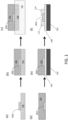
- FIG. 1 panels (a)-(f).
- the method begins with one or more nanostructures 102 disposed on a surface of a first substrate 100 ( FIG. 1 , panel (a)).
- a coating of a crosslinkable copolymer 104 is applied over the one or more nanostructures 102 and the exposed areas of the surface of the first substrate 100 ( FIG. 1 , panel (b)).
- Crosslinkable copolymer 104 is then heated to induce the crosslinking of the copolymer and bond formation between copolymer 104 and first substrate 100.
- First substrate 100 is then removed from nanostructures 102 and copolymer 104.
- the bonding of copolymer 104 to first substrate 100 via the heat treatment prior to substrate 100 removal is advantageous because the bonds can prevent the premature delamination of the one or more nanostructures 102 from copolymer 104 during the etching of first substrate 100.
- One or more released nanostructures 102 are then transferred onto a surface of a second substrate 108 ( FIG. 1 , panel (e)).
- the transferred nanostructures may then be annealed to bond the nanostructures to the second substrate.
- the second substrate may include more than one layer.
- the substrate may include a thin overlayer 108 supported by a thicker handle substrate 110.
- Copolymer 104 is then removed and additional device components can be fabricated on and/or around the one or more transferred nanostructures 102.
- a field-effect transistor can be fabricated using a SiO 2 /Si substrate (108/110) by depositing a source electrode 112 and a drain electrode 114 on a semiconducting nanostructure 102 ( FIG. 1 , panel (f)).
- the term nanostructure refers to a structure having at least one dimension (e.g., height, width, length, thickness, or diameter) that is no greater than 1 ⁇ m. This includes structures having at least one dimension that is no greater than 100 nm further includes structures having at least one dimension that is no greater than 10 nm, and still further includes structures having at least one dimension that is no greater than 1 nm.
- the nanostructures include structures having at least two dimensions (e.g., length and width) that fall within the above-recited size ranges and structures for which even the largest cross-section dimension falls within the above-recited size ranges.
- the one or more nanostructures may be composed of a variety of materials including inorganic semiconductors, metals (including metal alloys), and inorganic dielectric materials.
- Narrow, ultrathin, high-aspect ratio nanostructures are particularly good candidates for transfer using the methods described herein.
- existing methods for the transfer of narrow, ultrathin, high-aspect ratio nanostructures using PMMA homopolymer as a transfer medium typically have a poor transfer yield.
- the present methods are able to transfer even dense arrays of many nanostructures, including narrow, ultrathin, high-aspect ratio nanostructures, with transfer yields of, or approaching, 100%.
- Such arrays may include ten, hundreds, or thousands of nanostructures.
- Graphene nanostructures such as graphene nanoribbons, are examples of ultrathin, high-aspect ratio nanostructures.
- Monolayer graphene is a two-dimensional hexagonal network of sp 2 hybridized carbon atoms.
- Graphene nanoribbons are narrow, elongated strips (or "ribbons") of monolayer graphene having widths and crystallographic edge structures that provide the ribbons with electronic properties, such as electronic bandgaps, that are absent in continuous two-dimensional films of graphene.
- Nanoribbons can have aspect ratios of at least 5, at least 10, at least 100, or at least 1000.
- Graphene nanostructures may comprise monolayer graphene or multilayered graphene.
- the one or more nanostructures may have a variety of shapes, including hollow cylinders (e.g., nanotubes, including carbon nanotubes), solid cylinders (e.g., nanowires, including metal nanowires), and high aspect ratio thin strips (e.g., nanoribbons, including graphene nanoribbons and hexagonal boron nitride (h-BN) nanoribbons).
- a nanofilm is a type of nanostructure having the form of a layer of material having a thickness falling within the above-recited size ranges, but lateral dimensions (widths and lengths) that exceed 1 ⁇ m. Nanofilms include monolayer films of graphene and monolayer films of h-BN.
- First substrate 100 may be a substrate upon which the nanostructures are grown using, for example, chemical vapor deposition (CVD) growth.
- CVD chemical vapor deposition
- graphene can be grown on germanium (Ge) substrates via CVD.
- Other metal substrates upon which graphene can be grown include copper (Cu), ruthenium (Ru), nickel (Ni), palladium (Pd), iridium (Ir), and silicon carbide (SiC).
- the nanostructures may be grown in the form of nanostructures on the growth substrate (i.e., bottom-up growth) or may be lithographically patterned from a larger film of material that is grown on the growth substrate (i.e., top-down fabrication).
- first substrate 100 need not be a CVD growth substrate, or even a growth substrate.
- First substrate 100 may be any substrate on which the nanostructures are disposed that can be selectively removed from the nanostructures during the transfer process.
- first substrate 100 can be composed of a variety of materials, including inorganic materials, such as metals, semiconductors, and dielectric materials.
- Crosslinkable copolymer 104 is polymerized from a first monomer that lacks crosslinkable functional groups and a comonomer that introduces a crosslinkable functional group into the copolymer.
- the crosslinkable copolymer may be a random copolymer.
- a crosslinkable functional group is a functional group that is available to form crosslinks between copolymer backbone chains after the monomers have been polymerized.
- the first monomers that are incorporated into the copolymers do not participate in copolymer crosslinking in transfer methods described herein.
- the copolymers are polymerized from at least one monomer that is a non-crosslinking monomer, two or more non-crosslinking monomers can be incorporated into the copolymers.
- Suitable non-crosslinking monomers include methyl methacrylate monomers and/or methyl acrylate monomers (collectively referred to as methyl (meth)acrylate monomers), lactic acid monomers, phthalaldehyde monomers, bisphenol A carbonate monomers, and combinations of two or more thereof.
- the comomoners are monomers bearing crosslinkable functional groups.
- the crosslinkable functional groups form crosslinks between copolymer backbone chains and are also able to form bonds between copolymer 104 and first substrate 100.
- the bonds may be, for example, covalent bonds and/or ionic bonds.
- the copolymers are polymerized from at least one monomer bearing a crosslinkable group, two or more crosslinking monomers can be incorporated into the copolymers.
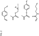
- Suitable crosslinkable groups include groups that undergo free-radical polymerization processes, such as epoxy groups, vinyl groups, and azide groups. Monomers bearing these groups include azido-substituted methacrylates, acrylates and styrenic monomers.
- These monomers which are described in Mansfeld, Ulrich, et al. Polymer Chemistry 1.10 (2010): 1560-1598 , include those having the structures shown in FIG. 2 . These structures can be expanded to o, p, and m substitution on the benzene ring and to include linkers from 1-12 methylene units in the acrylates and methacrylates.
- crosslinkable copolymers are polymerized from only one or more of the non-crosslinking monomers listed above and one more of the crosslinkable group-bearing monomers listed above.
- other non-crosslinking monomers and crosslinkable group-bearing monomers can be used.
- Copolymers of methyl (meth)acrylate and glycidyl methacrylate and/or glycidyl acrylate are one example of a crosslinkable copolymer that can be used.
- the copolymers may consist of only polymerized of methyl (meth)acrylate and glycidyl (meth)acrylate monomers.
- the layer of crosslinkable copolymer 104 is cured to induce crosslinking and substrate-copolymer bond formation.
- Thermal curing of the copolymer can be carried out by heating the copolymer to a temperature at which the crosslinkable groups undergo crosslinking reactions and copolymer-substrate bond formation.
- the optimal curing temperature will vary depending upon the particular comonomers and first substrates being used. Temperatures in the range from about 100 °C to about 250 °C are typically sufficient.
- the crosslinkable copolymers bond more strongly to the first substrate and, as a result, are able to transfer even very narrow nanostructures between substrates with high yields.
- the crosslinkable comonomers are a minor component in the copolymer; they are present at a concentration sufficient to provide enhanced substrate bonding and polymer rigidity, relative to a PMMA homopolymer.
- the concentration of polymerized crosslinkable monomers in the copolymers is desirably limited.
- the comonomers bearing the crosslinkable groups make up no more than 20 mol.% of the copolymer. This includes embodiments in which the comonomers bearing the crosslinkable groups make up no more than 10 mol.% of the copolymer, no more than 6 mol.% of the copolymer, and no more than 4 mol.% of the copolymer.
- the polymerized crosslinkable group-bearing comonomer may make up 1 mol.% to 20 mol.% of the copolymer, including embodiments in which the polymerized crosslinkable group-bearing comonomer make up from 2 mol.% to 8 mol.% of the copolymers.
- the balance of the copolymers is formed from polymerized non-crosslinking monomers.
- the copolymer layer should be sufficiently thick to facilitate handling during the nanostructure transfer process, but is not otherwise particularly limited. However, unnecessarily thick layers will extend the time needed to remove the copolymer. Generally, a thickness in the range from about 100 nm to 1 ⁇ m is sufficient. If cost or other concerns make it undesirable to use a thick layer of the copolymer, a thin layer of the copolymer can be applied to the nanostructures and a thicker layer of a second homopolymer or copolymer, such as a PMMA homopolymer, can be applied over the copolymer to provide a multilayered polymeric transfer medium.
- a second homopolymer or copolymer such as a PMMA homopolymer
- first substrate 100 can be selectively removed using, for example, a wet or dry etch. Suitable etchants will remove first substrate 100 without etching the one or more nanostructures 102 or the copolymer 104, and, therefore, etchant selection will depend on the particular substrates, nanostructures, and copolymers being used.
- a H 2 O:HF:H 2 O 2 etch can be used to selectively remove a Ge substrate, and an aqueous solution of iron nitrate or iron chloride can be used to remove a Cu substrate.
- Second substrate 108 may be composed of various materials, including metals, semiconductors, and dielectric materials. Inorganic and organic (e.g., polymer) substrates can be used. As shown in the embodiment of FIG. 1 , panel (e), second substrate 108 may be a multilayered substrate. For example, a substrate comprising a relatively thin layer 108, such as a dielectric layer, over a thicker support 110 can be used. Illustrative examples of substrates onto which the nanostructures can be transferred include SiO 2 /Si substrates, polyethylene terephthalate (PET) substrates, sapphire substrates, and mica substrates.
- PET polyethylene terephthalate
- the transfer to second substrate 108 can be a wet transfer or a dry transfer.
- the copolymer 104/nanostructure 102/first substrate 100 stack is submerged in wet etchant 106 to selectively remove first substrate 100.
- the resulting released copolymer 104/nanostructure 102 stack can then be transferred to and floated on the surface of a water bath.
- Second substrate 108/110 is then used to lift the copolymer 104/nanostructure 102 stack out of the water bath.
- the copolymer 104/nanostructure 102/second substrate 108/110 stack can then be dried.
- the copolymer 104/nanostructure 102/second substrate 108/110 stack can be heated to a temperature that promotes adhesion between one or more nanostructures 102 and the surface of the second substrate 108.
- temperatures in the range from about 100 °C to about 150 °C are sufficient.
- Copolymer 104 is then selectively removed from the one or more nanostructures 102.
- the removal of copolymer can be achieved with organic solvents, a thermal anneal, or a combination thereof.
- the copolymer is first solvated using a suitable solvent and any residual polymer is then removed during the thermal anneal.
- suitable solvents include acetone and N-methyl-2-pyrrolidone (NMP).
- NMP N-methyl-2-pyrrolidone
- Annealing temperatures in the range from 300 °C to 500 °C are typically suitable. However, temperatures outside of this range can be used.
- This example illustrates a method of transferring an array of graphene nanoribbons from a Ge CVD growth substrate to a SiO 2 /Si device substrate using a PMMA-GMA copolymer as a transfer medium.
- the transfer process is compared to an analogous transfer process in which a PMMA homopolymer is used as a transfer medium.
- a degenerately doped Si wafer with 15 nm of thermally grown SiO 2 was chosen as the transfer substrate because it can serve as a universal back-gate for the fabrication of a field-effect transistor (FET), as depicted in panel (f) of FIG.1 .
- FET field-effect transistor
- Graphene nanoribbons were grown via anisotropic CVD growth on a Ge(001) wafer. Methods for growing graphene nanoribbons via anisotropic CVD growth on Ge(001) are known and more details regarding these methods can be found in Way, Austin J., et al., The journal of physical chemistry letters 10.15 (2019): 4266-4272 and Way, Austin J., Robert M. Jacobberger, and Michael S. Arnold, Nano letters 18.2 (2018): 898-906 .
- the graphene nanoribbons were transferred to SiO 2 on Si using a PMMA-GMA copolymer.
- the copolymer was polymerized from 96 mol % methyl methacrylate (MMA) with 4 mol % of thermally crosslinkable glycidyl methacrylate (GMA), as described in Liu, C. et al., Macromolecules, 2011, 44 (7), 1876-1885 .
- MMA methyl methacrylate
- GMA thermally crosslinkable glycidyl methacrylate
- the PMMA-GMA (96% PMMA, 4% GMA) was spin-coated on the graphene nanoribbons and the exposed areas of the Ge(001) surface and then thermally annealed at 160 °C for 3 h in a vacuum to promote crosslinking and better bonding of the copolymer with the Ge substrate. Excess copolymer was removed by rinsing in toluene, resulting in a film that was 3 to 5 nm in thickness. For better handling, PMMA homopolymer was spin-coated on top of the PMMA-GMA film, and the substrate was annealed at 160 °C for 5 hours in an N 2 environment ( ⁇ 1 ppm O 2 and ⁇ 1 ppm H 2 O).
- the thickness of the PMMA layer was 1 ⁇ m.
- the backside of the sample that was uncoated with polymer underwent an O 2 plasma etch (50 W, 10 mTorr, 10 sccm of O 2 ) for 3 min (Unaxis 790 Reactive Ion Etcher) to remove graphene.
- the sample was then floated on 3:1:1 H 2 O:HF:H 2 O 2 to etch away the Ge substrate.
- the released nanoribbon/copolymer membrane was transferred from the Ge etchant to three successive H 2 O baths and finally to a piranha cleaned SiO 2 (15 nm) on Si substrate.
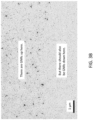
- FIG. 3A is an SEM image of the graphene nanoribbon array after the transfer to the SiO 2 showing that the graphene nanoribbons were uniformly transferred with a nearly 100% transfer yield over the 5 x 5 mm 2 surface area of the SiO 2 substrate.
- FIG. 3B is an SEM image of the graphene nanoribbon array after the transfer to the SiO 2 showing a poor graphene nanoribbon transfer yield of approximately 25%, with a large section (lower area) of the surface of the SiO 2 substrate having no transferred graphene nanoribbons.
Landscapes
- Chemical & Material Sciences (AREA)
- Organic Chemistry (AREA)
- Engineering & Computer Science (AREA)
- Materials Engineering (AREA)
- Nanotechnology (AREA)
- Inorganic Chemistry (AREA)
- Life Sciences & Earth Sciences (AREA)
- Wood Science & Technology (AREA)
- Carbon And Carbon Compounds (AREA)
- Addition Polymer Or Copolymer, Post-Treatments, Or Chemical Modifications (AREA)
Claims (16)
- Verfahren zum Übertragen einer oder mehrerer Nanostrukturen von einem ersten Substrat auf ein zweites Substrat, wobei das Verfahren Folgendes umfasst:Auftragen einer Beschichtung aus einem vernetzbaren Copolymer über einer oder mehreren Nanostrukturen auf einer Oberfläche des ersten Substrats, wobei das vernetzbare Copolymer aus einem oder mehreren nicht vernetzenden Monomeren und einem oder mehreren Comonomeren, die vernetzbare Gruppen tragen, polymerisiert ist;Erhitzen des vernetzbaren Copolymers, um eine Vernetzung des vernetzbaren Copolymers zu induzieren und um Bindungen zwischen dem vernetzbaren Copolymer und der Oberfläche des ersten Substrats zu bilden;Freigeben der einen oder mehreren Nanostrukturen und des vernetzten Copolymers aus dem ersten Substrat;Übertragen der einen oder mehreren Nanostrukturen und des vernetzten Copolymers auf eine Oberfläche des zweiten Substrats; undEntfernen des vernetzten Copolymers aus der einen oder den mehreren Nanostrukturen.
- Verfahren nach Anspruch 1, wobei die vernetzbaren Gruppen Epoxygruppen, Azidgruppen, Vinylgruppen oder eine Kombination davon umfassen.
- Verfahren nach Anspruch 1, wobei das eine oder die mehreren nicht vernetzenden Monomere Methyl(meth)acrylatmonomere umfassen.
- Verfahren nach Anspruch 1, wobei das eine oder die mehreren Comonomere Glycidyl(meth)acrylatmonomere umfassen.
- Verfahren nach Anspruch 3, wobei das eine oder die mehreren Comonomere Glycidyl(meth)acrylatmonomere umfassen.
- Verfahren nach Anspruch 1, wobei das eine oder die mehreren Comonomere Milchsäuremonomere, Phthalaldehydmonomere, Bisphenol-A-Carbonatmonomere oder eine Kombination davon umfassen.
- Verfahren nach Anspruch 3, wobei das eine oder die mehreren Comonomere Milchsäuremonomere, Phthalaldehydmonomere, Bisphenol-A-Carbonatmonomere oder eine Kombination davon umfassen.
- Verfahren nach Anspruch 1, wobei das vernetzbare Copolymer von 1 Mol.-% bis 20 Mol.-% der polymerisierten Comonomere und von 99 Mol.-% bis 80 Mol.-% der polymerisierten nicht vernetzenden Monomere umfasst.
- Verfahren nach Anspruch 1, wobei das vernetzbare Copolymer von 2 Mol.-% bis 8 Mol.-% der polymerisierten Comonomere und von 98 Mol.-% bis 92 Mol.-% der polymerisierten nicht vernetzenden Monomere umfasst.
- Verfahren nach Anspruch 1, wobei das vernetzbare Copolymer nur aus polymerisierten Methyl(meth)acrylatmonomeren und polymerisierten Glycidyl(meth)acrylatmonomeren besteht.
- Verfahren nach Anspruch 8, wobei das vernetzbare Copolymer nur aus polymerisierten Methyl(meth)acrylatmonomeren und polymerisierten Glycidyl(meth)acrylatmonomeren besteht.
- Verfahren nach Anspruch 11, wobei die eine oder mehreren Nanostrukturen Graphen-Nanobänder umfassen.
- Verfahren nach Anspruch 12, wobei das erste Substrat ein Germaniumsubstrat ist.
- Verfahren nach Anspruch 1, wobei die eine oder mehreren Nanostrukturen Graphen-Nanobänder umfassen.
- Verfahren nach Anspruch 14, wobei das erste Substrat ein Germaniumsubstrat ist.
- Verfahren nach Anspruch 1, ferner umfassend das Erhitzen der übertragenen einen oder mehreren Nanostrukturen und des zweiten Substrats, um Bindungen zwischen der einen oder den mehreren Nanostrukturen und dem zweiten Substrat zu bilden, bevor das vernetzte Copolymer aus der einen oder den mehreren Nanostrukturen entfernt wird.
Applications Claiming Priority (2)
| Application Number | Priority Date | Filing Date | Title |
|---|---|---|---|
| US17/209,944 US12077438B2 (en) | 2021-03-23 | 2021-03-23 | Transfer of nanostructures using crosslinkable copolymer films |
| PCT/US2022/070884 WO2022204645A1 (en) | 2021-03-23 | 2022-03-01 | Transfer of nanostructures using crosslinkable copolymer films |
Publications (3)
| Publication Number | Publication Date |
|---|---|
| EP4285392A1 EP4285392A1 (de) | 2023-12-06 |
| EP4285392A4 EP4285392A4 (de) | 2024-08-07 |
| EP4285392B1 true EP4285392B1 (de) | 2025-05-07 |
Family
ID=83363140
Family Applications (1)
| Application Number | Title | Priority Date | Filing Date |
|---|---|---|---|
| EP22776810.8A Active EP4285392B1 (de) | 2021-03-23 | 2022-03-01 | Übertragung von nanostrukturen unter verwendung von vernetzbaren copolymerfolien |
Country Status (5)
| Country | Link |
|---|---|
| US (1) | US12077438B2 (de) |
| EP (1) | EP4285392B1 (de) |
| KR (1) | KR102958289B1 (de) |
| TW (1) | TWI887527B (de) |
| WO (1) | WO2022204645A1 (de) |
Families Citing this family (2)
| Publication number | Priority date | Publication date | Assignee | Title |
|---|---|---|---|---|
| US12077438B2 (en) * | 2021-03-23 | 2024-09-03 | Wisconsin Alumni Research Foundation | Transfer of nanostructures using crosslinkable copolymer films |
| US20240047203A1 (en) * | 2022-08-04 | 2024-02-08 | Future Semiconductor Business, Inc | Monolithic remote epitaxy of compound semi conductors and 2d materials |
Family Cites Families (13)
| Publication number | Priority date | Publication date | Assignee | Title |
|---|---|---|---|---|
| BR0115030A (pt) | 2000-10-31 | 2004-06-15 | Kimberly Clark Co | Material de transferência de calor com filme descascável e revestimentos reticulados |
| EP1904670B1 (de) * | 2005-06-28 | 2011-09-28 | The Board of Regents of the University of Oklahoma | Verfahren zur züchtung und entnahme von kohlenstoffnanoröhren |
| CN103964422A (zh) | 2014-04-25 | 2014-08-06 | 无锡格菲电子薄膜科技有限公司 | 一种石墨烯转移方法 |
| WO2016071780A1 (en) | 2014-11-04 | 2016-05-12 | Sabic Global Technologies B.V. | Direct transfer of multiple graphene layers onto multiple target substrates |
| US10106643B2 (en) * | 2015-03-31 | 2018-10-23 | 3M Innovative Properties Company | Dual-cure nanostructure transfer film |
| WO2016201234A1 (en) * | 2015-06-12 | 2016-12-15 | Lintec Corporation | Carbon nanotube forest laminated body and method of producing caron nanotube forest laminated body |
| CN107364851B (zh) | 2016-11-28 | 2019-08-16 | 中国科学院金属研究所 | 一种松香树脂转移石墨烯的方法及石墨烯透明导电薄膜的制备与应用 |
| CN110092351B (zh) * | 2018-01-27 | 2022-08-16 | 清华大学 | 利用碳纳米管膜转移二维纳米材料的方法 |
| KR102117954B1 (ko) | 2018-02-22 | 2020-06-02 | 성균관대학교산학협력단 | 그래핀 전사용 고분자 및 이를 이용한 그래핀의 전사 방법 |
| US11106107B2 (en) * | 2018-09-09 | 2021-08-31 | Zhejiang Jingyi New Material Technology Co., Ltd | Ultra-flexible and robust silver nanowire films for controlling light transmission and method of making the same |
| CN111128637B (zh) | 2018-11-01 | 2021-02-26 | 清华大学 | 场发射体的制备方法 |
| CN110156001B (zh) | 2019-07-11 | 2023-01-03 | 电子科技大学 | 一种转移石墨烯薄膜的方法 |
| US12077438B2 (en) * | 2021-03-23 | 2024-09-03 | Wisconsin Alumni Research Foundation | Transfer of nanostructures using crosslinkable copolymer films |
-
2021
- 2021-03-23 US US17/209,944 patent/US12077438B2/en active Active
-
2022
- 2022-03-01 KR KR1020237033914A patent/KR102958289B1/ko active Active
- 2022-03-01 EP EP22776810.8A patent/EP4285392B1/de active Active
- 2022-03-01 WO PCT/US2022/070884 patent/WO2022204645A1/en not_active Ceased
- 2022-03-03 TW TW111107731A patent/TWI887527B/zh active
Also Published As
| Publication number | Publication date |
|---|---|
| US20220306475A1 (en) | 2022-09-29 |
| WO2022204645A1 (en) | 2022-09-29 |
| KR102958289B1 (ko) | 2026-04-27 |
| TWI887527B (zh) | 2025-06-21 |
| EP4285392A1 (de) | 2023-12-06 |
| KR20230159456A (ko) | 2023-11-21 |
| EP4285392A4 (de) | 2024-08-07 |
| US12077438B2 (en) | 2024-09-03 |
| TW202240708A (zh) | 2022-10-16 |
Similar Documents
| Publication | Publication Date | Title |
|---|---|---|
| EP2300214B1 (de) | Verfahren zur herstellung periodischer strukturen auf polymeren unter verwendung von plasmaprozessen | |
| KR102109380B1 (ko) | 절연기판상에 그래핀 단일층을 제조하는 방법 | |
| US9758381B2 (en) | Method to transfer two dimensional film grown on metal-coated wafer to the wafer itself in a face-to face manner | |
| US8748296B2 (en) | Edge-exclusion spalling method for improving substrate reusability | |
| US10814597B2 (en) | Method for preparing suspended two-dimensional nanomaterials | |
| Gowrishankar et al. | Fabrication of densely packed, well-ordered, high-aspect-ratio silicon nanopillars over large areas using block copolymer lithography | |
| US20080311347A1 (en) | Alternating Self-Assembling Morphologies of Diblock Copolymers Controlled by Variations in Surfaces | |
| US12077438B2 (en) | Transfer of nanostructures using crosslinkable copolymer films | |
| US10889914B2 (en) | Location-specific growth and transfer of single crystalline TMD monolayer arrays | |
| CN112194120A (zh) | 使用极化的铁电聚合物无缺陷地直接干法层离cvd石墨烯 | |
| Du et al. | Dual applications of free-standing holographic nanopatterns for lift-off and stencil lithography | |
| EP1559678A2 (de) | Nanostrukuren und Herstellungsverfahren für diese | |
| US10646831B2 (en) | Method for manufacturing of a carbon nanomembrane | |
| US11033862B2 (en) | Method of manufacturing partially freestanding two-dimensional crystal film and device comprising such a film | |
| CN113488373B (zh) | 一种干法制备单层二维半导体阵列的方法 | |
| US11226555B2 (en) | Preparing patterned neutral layers and structures prepared using the same | |
| Frommhold et al. | High aspect ratio silicon and polyimide nanopillars by combination of nanosphere lithography and intermediate mask pattern transfer | |
| US10814598B2 (en) | Method for transferring two-dimensional nanomaterials | |
| CN111320164A (zh) | 一种悬空石墨烯结构的制备方法及由其得到的悬空石墨烯结构和应用 | |
| Lee et al. | Graphene-enabled block copolymer lithography transfer to arbitrary substrates | |
| US20230324788A1 (en) | Graphene-enabled Block Copolymer Lithography Transfer to Arbitrary Surfaces | |
| Vendamani et al. | Fabrication of silver honey comb nano template | |
| Min et al. | Fabrication of Aperture-Tunable Silicon Nanostencil Membrane via Localized Laser Annealing | |
| US20100133716A1 (en) | Method of forming relief structures | |
| GB2587611A (en) | A method for producing polymeric surface modification layers |
Legal Events
| Date | Code | Title | Description |
|---|---|---|---|
| STAA | Information on the status of an ep patent application or granted ep patent |
Free format text: STATUS: THE INTERNATIONAL PUBLICATION HAS BEEN MADE |
|
| PUAI | Public reference made under article 153(3) epc to a published international application that has entered the european phase |
Free format text: ORIGINAL CODE: 0009012 |
|
| STAA | Information on the status of an ep patent application or granted ep patent |
Free format text: STATUS: REQUEST FOR EXAMINATION WAS MADE |
|
| 17P | Request for examination filed |
Effective date: 20230901 |
|
| AK | Designated contracting states |
Kind code of ref document: A1 Designated state(s): AL AT BE BG CH CY CZ DE DK EE ES FI FR GB GR HR HU IE IS IT LI LT LU LV MC MK MT NL NO PL PT RO RS SE SI SK SM TR |
|
| DAV | Request for validation of the european patent (deleted) | ||
| DAX | Request for extension of the european patent (deleted) | ||
| A4 | Supplementary search report drawn up and despatched |
Effective date: 20240709 |
|
| RIC1 | Information provided on ipc code assigned before grant |
Ipc: C09D 133/06 20060101ALI20240703BHEP Ipc: C08F 220/32 20060101ALI20240703BHEP Ipc: C08F 220/14 20060101ALI20240703BHEP Ipc: C01B 32/186 20170101ALI20240703BHEP Ipc: C01B 32/194 20170101ALI20240703BHEP Ipc: H01B 5/14 20060101ALI20240703BHEP Ipc: H01B 13/00 20060101AFI20240703BHEP |
|
| GRAP | Despatch of communication of intention to grant a patent |
Free format text: ORIGINAL CODE: EPIDOSNIGR1 |
|
| STAA | Information on the status of an ep patent application or granted ep patent |
Free format text: STATUS: GRANT OF PATENT IS INTENDED |
|
| INTG | Intention to grant announced |
Effective date: 20241213 |
|
| GRAS | Grant fee paid |
Free format text: ORIGINAL CODE: EPIDOSNIGR3 |
|
| P01 | Opt-out of the competence of the unified patent court (upc) registered |
Free format text: CASE NUMBER: APP_4059/2025 Effective date: 20250124 |
|
| GRAA | (expected) grant |
Free format text: ORIGINAL CODE: 0009210 |
|
| STAA | Information on the status of an ep patent application or granted ep patent |
Free format text: STATUS: THE PATENT HAS BEEN GRANTED |
|
| AK | Designated contracting states |
Kind code of ref document: B1 Designated state(s): AL AT BE BG CH CY CZ DE DK EE ES FI FR GB GR HR HU IE IS IT LI LT LU LV MC MK MT NL NO PL PT RO RS SE SI SK SM TR |
|
| REG | Reference to a national code |
Ref country code: GB Ref legal event code: FG4D |
|
| REG | Reference to a national code |
Ref country code: CH Ref legal event code: EP |
|
| REG | Reference to a national code |
Ref country code: DE Ref legal event code: R096 Ref document number: 602022014427 Country of ref document: DE |
|
| REG | Reference to a national code |
Ref country code: IE Ref legal event code: FG4D |
|
| REG | Reference to a national code |
Ref country code: NL Ref legal event code: MP Effective date: 20250507 |
|
| PG25 | Lapsed in a contracting state [announced via postgrant information from national office to epo] |
Ref country code: ES Free format text: LAPSE BECAUSE OF FAILURE TO SUBMIT A TRANSLATION OF THE DESCRIPTION OR TO PAY THE FEE WITHIN THE PRESCRIBED TIME-LIMIT Effective date: 20250507 Ref country code: FI Free format text: LAPSE BECAUSE OF FAILURE TO SUBMIT A TRANSLATION OF THE DESCRIPTION OR TO PAY THE FEE WITHIN THE PRESCRIBED TIME-LIMIT Effective date: 20250507 Ref country code: PT Free format text: LAPSE BECAUSE OF FAILURE TO SUBMIT A TRANSLATION OF THE DESCRIPTION OR TO PAY THE FEE WITHIN THE PRESCRIBED TIME-LIMIT Effective date: 20250908 |
|
| REG | Reference to a national code |
Ref country code: LT Ref legal event code: MG9D |
|
| PG25 | Lapsed in a contracting state [announced via postgrant information from national office to epo] |
Ref country code: NO Free format text: LAPSE BECAUSE OF FAILURE TO SUBMIT A TRANSLATION OF THE DESCRIPTION OR TO PAY THE FEE WITHIN THE PRESCRIBED TIME-LIMIT Effective date: 20250807 Ref country code: GR Free format text: LAPSE BECAUSE OF FAILURE TO SUBMIT A TRANSLATION OF THE DESCRIPTION OR TO PAY THE FEE WITHIN THE PRESCRIBED TIME-LIMIT Effective date: 20250808 |
|
| PG25 | Lapsed in a contracting state [announced via postgrant information from national office to epo] |
Ref country code: NL Free format text: LAPSE BECAUSE OF FAILURE TO SUBMIT A TRANSLATION OF THE DESCRIPTION OR TO PAY THE FEE WITHIN THE PRESCRIBED TIME-LIMIT Effective date: 20250507 Ref country code: PL Free format text: LAPSE BECAUSE OF FAILURE TO SUBMIT A TRANSLATION OF THE DESCRIPTION OR TO PAY THE FEE WITHIN THE PRESCRIBED TIME-LIMIT Effective date: 20250507 |
|
| REG | Reference to a national code |
Ref country code: AT Ref legal event code: MK05 Ref document number: 1793433 Country of ref document: AT Kind code of ref document: T Effective date: 20250507 |
|
| PG25 | Lapsed in a contracting state [announced via postgrant information from national office to epo] |
Ref country code: BG Free format text: LAPSE BECAUSE OF FAILURE TO SUBMIT A TRANSLATION OF THE DESCRIPTION OR TO PAY THE FEE WITHIN THE PRESCRIBED TIME-LIMIT Effective date: 20250507 |
|
| PG25 | Lapsed in a contracting state [announced via postgrant information from national office to epo] |
Ref country code: HR Free format text: LAPSE BECAUSE OF FAILURE TO SUBMIT A TRANSLATION OF THE DESCRIPTION OR TO PAY THE FEE WITHIN THE PRESCRIBED TIME-LIMIT Effective date: 20250507 |
|
| PG25 | Lapsed in a contracting state [announced via postgrant information from national office to epo] |
Ref country code: AT Free format text: LAPSE BECAUSE OF FAILURE TO SUBMIT A TRANSLATION OF THE DESCRIPTION OR TO PAY THE FEE WITHIN THE PRESCRIBED TIME-LIMIT Effective date: 20250507 |
|
| PG25 | Lapsed in a contracting state [announced via postgrant information from national office to epo] |
Ref country code: RS Free format text: LAPSE BECAUSE OF FAILURE TO SUBMIT A TRANSLATION OF THE DESCRIPTION OR TO PAY THE FEE WITHIN THE PRESCRIBED TIME-LIMIT Effective date: 20250807 |
|
| PG25 | Lapsed in a contracting state [announced via postgrant information from national office to epo] |
Ref country code: IS Free format text: LAPSE BECAUSE OF FAILURE TO SUBMIT A TRANSLATION OF THE DESCRIPTION OR TO PAY THE FEE WITHIN THE PRESCRIBED TIME-LIMIT Effective date: 20250907 |
|
| PG25 | Lapsed in a contracting state [announced via postgrant information from national office to epo] |
Ref country code: LV Free format text: LAPSE BECAUSE OF FAILURE TO SUBMIT A TRANSLATION OF THE DESCRIPTION OR TO PAY THE FEE WITHIN THE PRESCRIBED TIME-LIMIT Effective date: 20250507 |
|
| PG25 | Lapsed in a contracting state [announced via postgrant information from national office to epo] |
Ref country code: DK Free format text: LAPSE BECAUSE OF FAILURE TO SUBMIT A TRANSLATION OF THE DESCRIPTION OR TO PAY THE FEE WITHIN THE PRESCRIBED TIME-LIMIT Effective date: 20250507 Ref country code: SM Free format text: LAPSE BECAUSE OF FAILURE TO SUBMIT A TRANSLATION OF THE DESCRIPTION OR TO PAY THE FEE WITHIN THE PRESCRIBED TIME-LIMIT Effective date: 20250507 |
|
| PG25 | Lapsed in a contracting state [announced via postgrant information from national office to epo] |
Ref country code: CZ Free format text: LAPSE BECAUSE OF FAILURE TO SUBMIT A TRANSLATION OF THE DESCRIPTION OR TO PAY THE FEE WITHIN THE PRESCRIBED TIME-LIMIT Effective date: 20250507 |
|
| PG25 | Lapsed in a contracting state [announced via postgrant information from national office to epo] |
Ref country code: EE Free format text: LAPSE BECAUSE OF FAILURE TO SUBMIT A TRANSLATION OF THE DESCRIPTION OR TO PAY THE FEE WITHIN THE PRESCRIBED TIME-LIMIT Effective date: 20250507 |
|
| PG25 | Lapsed in a contracting state [announced via postgrant information from national office to epo] |
Ref country code: SK Free format text: LAPSE BECAUSE OF FAILURE TO SUBMIT A TRANSLATION OF THE DESCRIPTION OR TO PAY THE FEE WITHIN THE PRESCRIBED TIME-LIMIT Effective date: 20250507 |
|
| PG25 | Lapsed in a contracting state [announced via postgrant information from national office to epo] |
Ref country code: IT Free format text: LAPSE BECAUSE OF FAILURE TO SUBMIT A TRANSLATION OF THE DESCRIPTION OR TO PAY THE FEE WITHIN THE PRESCRIBED TIME-LIMIT Effective date: 20250507 |
|
| REG | Reference to a national code |
Ref country code: DE Ref legal event code: R097 Ref document number: 602022014427 Country of ref document: DE |
|
| PLBE | No opposition filed within time limit |
Free format text: ORIGINAL CODE: 0009261 |
|
| STAA | Information on the status of an ep patent application or granted ep patent |
Free format text: STATUS: NO OPPOSITION FILED WITHIN TIME LIMIT |
|
| REG | Reference to a national code |
Ref country code: CH Ref legal event code: L10 Free format text: ST27 STATUS EVENT CODE: U-0-0-L10-L00 (AS PROVIDED BY THE NATIONAL OFFICE) Effective date: 20260318 |
|
| 26N | No opposition filed |
Effective date: 20260210 |