EP4284625B1 - Nanostrukturierte oberflächenbeschichtung zur erzeugung neuartiger visueller erscheinungen - Google Patents
Nanostrukturierte oberflächenbeschichtung zur erzeugung neuartiger visueller erscheinungen Download PDFInfo
- Publication number
- EP4284625B1 EP4284625B1 EP22705434.3A EP22705434A EP4284625B1 EP 4284625 B1 EP4284625 B1 EP 4284625B1 EP 22705434 A EP22705434 A EP 22705434A EP 4284625 B1 EP4284625 B1 EP 4284625B1
- Authority
- EP
- European Patent Office
- Prior art keywords
- nanoparticles
- layer
- surface coating
- nanostructured surface
- particles
- Prior art date
- Legal status (The legal status is an assumption and is not a legal conclusion. Google has not performed a legal analysis and makes no representation as to the accuracy of the status listed.)
- Active
Links
Images

Classifications
-
- B—PERFORMING OPERATIONS; TRANSPORTING
- B29—WORKING OF PLASTICS; WORKING OF SUBSTANCES IN A PLASTIC STATE IN GENERAL
- B29C—SHAPING OR JOINING OF PLASTICS; SHAPING OF MATERIAL IN A PLASTIC STATE, NOT OTHERWISE PROVIDED FOR; AFTER-TREATMENT OF THE SHAPED PRODUCTS, e.g. REPAIRING
- B29C59/00—Surface shaping of articles, e.g. embossing; Apparatus therefor
- B29C59/02—Surface shaping of articles, e.g. embossing; Apparatus therefor by mechanical means, e.g. pressing
- B29C59/022—Surface shaping of articles, e.g. embossing; Apparatus therefor by mechanical means, e.g. pressing characterised by the disposition or the configuration, e.g. dimensions, of the embossments or the shaping tools therefor
-
- G—PHYSICS
- G02—OPTICS
- G02B—OPTICAL ELEMENTS, SYSTEMS OR APPARATUS
- G02B5/00—Optical elements other than lenses
- G02B5/02—Diffusing elements; Afocal elements
- G02B5/0205—Diffusing elements; Afocal elements characterised by the diffusing properties
- G02B5/021—Diffusing elements; Afocal elements characterised by the diffusing properties the diffusion taking place at the element's surface, e.g. by means of surface roughening or microprismatic structures
- G02B5/0226—Diffusing elements; Afocal elements characterised by the diffusing properties the diffusion taking place at the element's surface, e.g. by means of surface roughening or microprismatic structures having particles on the surface
-
- G—PHYSICS
- G02—OPTICS
- G02B—OPTICAL ELEMENTS, SYSTEMS OR APPARATUS
- G02B5/00—Optical elements other than lenses
- G02B5/02—Diffusing elements; Afocal elements
- G02B5/0273—Diffusing elements; Afocal elements characterized by the use
- G02B5/0294—Diffusing elements; Afocal elements characterized by the use adapted to provide an additional optical effect, e.g. anti-reflection or filter
-
- B—PERFORMING OPERATIONS; TRANSPORTING
- B29—WORKING OF PLASTICS; WORKING OF SUBSTANCES IN A PLASTIC STATE IN GENERAL
- B29C—SHAPING OR JOINING OF PLASTICS; SHAPING OF MATERIAL IN A PLASTIC STATE, NOT OTHERWISE PROVIDED FOR; AFTER-TREATMENT OF THE SHAPED PRODUCTS, e.g. REPAIRING
- B29C59/00—Surface shaping of articles, e.g. embossing; Apparatus therefor
- B29C59/02—Surface shaping of articles, e.g. embossing; Apparatus therefor by mechanical means, e.g. pressing
- B29C59/022—Surface shaping of articles, e.g. embossing; Apparatus therefor by mechanical means, e.g. pressing characterised by the disposition or the configuration, e.g. dimensions, of the embossments or the shaping tools therefor
- B29C2059/023—Microembossing
-
- B—PERFORMING OPERATIONS; TRANSPORTING
- B29—WORKING OF PLASTICS; WORKING OF SUBSTANCES IN A PLASTIC STATE IN GENERAL
- B29C—SHAPING OR JOINING OF PLASTICS; SHAPING OF MATERIAL IN A PLASTIC STATE, NOT OTHERWISE PROVIDED FOR; AFTER-TREATMENT OF THE SHAPED PRODUCTS, e.g. REPAIRING
- B29C59/00—Surface shaping of articles, e.g. embossing; Apparatus therefor
- B29C59/02—Surface shaping of articles, e.g. embossing; Apparatus therefor by mechanical means, e.g. pressing
- B29C2059/028—Incorporating particles by impact in the surface, e.g. using fluid jets or explosive forces to implant particles
-
- B—PERFORMING OPERATIONS; TRANSPORTING
- B29—WORKING OF PLASTICS; WORKING OF SUBSTANCES IN A PLASTIC STATE IN GENERAL
- B29C—SHAPING OR JOINING OF PLASTICS; SHAPING OF MATERIAL IN A PLASTIC STATE, NOT OTHERWISE PROVIDED FOR; AFTER-TREATMENT OF THE SHAPED PRODUCTS, e.g. REPAIRING
- B29C59/00—Surface shaping of articles, e.g. embossing; Apparatus therefor
- B29C59/02—Surface shaping of articles, e.g. embossing; Apparatus therefor by mechanical means, e.g. pressing
- B29C59/026—Surface shaping of articles, e.g. embossing; Apparatus therefor by mechanical means, e.g. pressing of layered or coated substantially flat surfaces
Definitions
- the present disclosure relates to the field of interaction between light and the surface of an object. More particularly, the present disclosure relates to a nanostructured surface coating capable of controlling the interaction between light and the nanostructured surface to generate novel visual appearances.
- the visual appearance of an object results from the interaction between light and the material constituting the surface of the object.
- the visual appearances of an object are classified mainly into five classes: shape, texture, gloss, translucency, color.
- the first classes of appearance are more geometric attributes and the last three are related to the nature of the object. For example, it is known that color arises from the selective absorption by matter and the diffusion of unabsorbed light.
- the brightness of the surface of an object comes from the reflection of light on the external surface of the object.
- Translucency results from the volume and surface diffusion properties of the object.
- the present disclosure provides a nanostructured surface composed of particles having a high refractive index, of nanometric dimension (of the order of tens or hundreds of nanometers) and a random but controlled spatial distribution to induce strong interferences between lights scattered by the particles in order to generate new appearances that feature colors resilient to lighting and viewing directions and appearances that vary with those directions.
- the scattering of light is governed by the size, shape, optical index, arrangement and density of the particles dispersed in a medium that is homogeneous. Interference between the light scattered by the scattering centers that are these particles can then play an important role in the generation of visual appearances.
- the nanostructured surface is considered as a two-dimensional system; that is, a layer of finite and constant thickness.
- the document FR 3 073 321 A1 describes a nanostructured surface coating according to the preamble of claim 1.
- This disclosure improves the situation.
- the second layer is made of a material whose refractive index is between 1.3 and 2 and chosen from the following materials: SiO 2 , sol gel, TiO2, Sl 3 N 4 , polymers and oxides.
- the substrate is made of a material with a refractive index between 1.3 and 4 and chosen from the following materials: Si, AsGa, quartz, silica, polymer.
- the material forming the first layer in which the nanoparticles are dispersed has a refractive index n p of between 1 and 2, n p being chosen so as to be lower than the refractive index of the nanoparticles.
- Nanoparticles are made of a material with a refractive index greater than or equal to 1.4.
- the nanoparticles are made of a dielectric or metallic material chosen from one of the following materials: silver, gold, aluminum, silicon, germanium, titanium dioxide, polymer, silicon nitride.
- Nanoparticles have a cylindrical shape, a spherical shape, a cubic shape or any other geometric shape.
- the nanoparticles have a surface filling rate f of between 5 and 30%.
- a nanostructured surface coating 1 according to a first embodiment is described below. This coating is intended in particular to generate new visual appearances resulting from interferences related to diffuse light and specular light by the nanostructured surface.
- the nanostructured surface coating comprises a first layer comprising a random distribution of nanoparticles 2 and a substrate 3 on which the layer of nanoparticles 2 is arranged.
- the substrate defines a surface in a plane (X, Y) which according to the disclosure is planar or slightly rough.
- the first layer of nanoparticles is formed by a set of nanoparticles randomly distributed on the surface of the substrate.
- the particles are incorporated into a protective layer.
- the protective layer is made of a material with a low refractive index of between 1 and 2.
- the protective layer is made of SiO 2 or plastic.
- the protective layer has a thickness of between a few hundred nanometers and several hundred micrometers.
- the nanoparticles are randomly distributed in the (X, Y) plane.
- the particles In the Z direction which is perpendicular to the (X, Y) plane, the particles have a substantially constant height and form a monolayer of particles.
- the particles In an exemplary embodiment illustrated in the figure 1 , the particles have an ellipsoidal shape and are oriented with the same height corresponding to the thickness of the monolayer.
- the radius of the sphere corresponds to the thickness of the monolayer.
- the height of the cylinder corresponds to the thickness of the monolayer.
- Nanoparticles have a complex optical refractive index n+ik, n being the real part corresponding to the refractive index and k the imaginary part called the extinction coefficient. Nanoparticles have an optical refractive index higher than that of the protective layer.
- the particles have a high optical index between 1.4 and 4 in order to strongly scatter the incident light.
- the particles can be made of a metallic material with high indices, for example gold, silver or aluminum. They can also be made of a dielectric material with high indices, for example silicon or titanium dioxide. They can also be made of polystyrene; they then have an index of approximately 1.5, capable of producing new effects.
- Particles have a geometric radius denoted R which is less than the wavelength of the visible spectrum. They can have different geometric shapes, spheres, cubes, rods. By geometric radius, we mean the radius of a smallest circle that encloses the particle. Particles can be spherical particles, cylindrical particles, particles. In the case where the particle is a sphere or a cylinder, the geometric radius corresponds to the radius of the particle. The geometric radius is generally between 30 nm and 300 nm, preferably between 70 nm and 150 nm. Due to its nanometric dimension, in the remainder of the description, the particles are designated by the term “nanoparticles” and the surface of the layer comprising the nanoparticles by the term “nanostructured surface”.
- the surface filling rate is between 0.01 and 0.7, preferably between 0.01 and 0.35.
- surface filling rate is meant the ratio between the sum of the cross-sections of the particles and the total surface area of the layer.
- n p is the index of the protective layer in which the nanoparticles are incorporated.
- the distance between the particles d must be less than or equal to the effective wavelength to observe the visual effects.
- the effective wavelength is the wavelength seen by the particles incorporated in the protective layer. The wavelength therefore corresponds to the longest wavelength of the visible spectrum in the material of the protective layer.
- the distance between the particles d must be greater than or equal to 2R. The lower bound is imposed by the fact that the particles are considered impenetrable.
- each particle Due to the high optical index of refraction, each particle can localize light at a scale smaller than the visible wavelength. Due to the high localization of the particles, they can be placed relative to each other at a distance smaller than the wavelength while forming individual scattering centers.
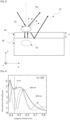
- the nanoparticles When the nanoparticles are illuminated by an incident visible light ray RI, the ray is reflected by the particles in the form of the scattered rays RD and a specular ray RS.
- the interference between the beams scattered by the particles can generate bright scattering colors that change on the object when the direction of the light illuminating the particles changes or when the observation direction of the particles moves, thus generating the iridescence effect.
- n p 1.5
- d must be between 120 nm and 493 nm.
- the surface filling rate f is equal to 10%. The light illuminates the structure with an angle of incidence of 30° and it is unpolarized.
- the two diffuse reflectance spectra in graph (a) show a shift of the resonance peaks towards longer wavelengths as the particle size increases.
- the resonance peaks are located around 440 and 520 nm.
- the resonance peaks are located around 600 and 750 nm.
- the colors related to diffuse reflectance depend mainly on the spectrum of each particle.
- the two specular reflectance spectra (b) show similar resonances.
- the nanostructured surface coating makes it possible to generate diffuse and specular colors different from each other depending on the illumination direction of the incident light and the observation direction.
- a nanostructured surface coating 10 according to a second embodiment is described below.
- the nanostructured surface coating comprises a first layer comprising a random distribution of nanoparticles 20, a substrate 40 and a second layer 30 arranged between the first layer 20 and the substrate 40.
- the substrate defines a surface in a plane (X, Y).
- the second layer 30 is deposited on the substrate.
- the set of nanoparticles 20 are randomly distributed on the surface of the second layer 30.
- the first layer of nanoparticles is formed only from a set of nanoparticles randomly distributed on the surface of the second layer 30.
- the particles are incorporated in a protective layer which extends in the plane (X, Y).
- the protective layer is made of a material with a low refractive index.
- the protective layer is made of SiO 2 or plastic.
- the protective layer has a thickness of between a few hundred nanometers and several hundred micrometers.
- the nanoparticles are first deposited on the substrate 40. Once the monolayer of nanoparticles has been produced, a protective layer is deposited on the substrate.
- the second layer 30, called the nanoparticle support layer is made of a material with a low refractive index n sup of between 1.3 and 2.
- the material can be chosen from the following materials: SiO2, TiO2, polymer, Si 3 N 4 , sol gels and oxides.
- This second layer has a thickness of between 0 and 1 ⁇ m.
- the structure of the second layer 30 is a multilayer structure.
- the second layer 30 comprises a semi-transparent or opaque thin metallic layer and a layer of SiO 2 , with the thin metallic layer deposited on the substrate and the layer of nanoparticles deposited on the layer of SiO 2 which acts as a support layer.
- the second layer 30 may be a stack of layers forming a Bragg mirror or a dielectric mirror arranged between the substrate 40 and the layer of nanoparticles 20.
- the substrate does not need to be reflective and therefore does not need to be made of a material with a high refractive index.
- the substrate is made of a material with a high refractive index between 2 and 4 to reflect and form the virtual image 50 of the nanoparticle.
- the material can be a semiconductor or a metal.
- the nanoparticles are randomly distributed in the (X, Y) plane.
- the particles In the Z direction which is perpendicular to the (X, Y) plane, the particles have a substantially constant thickness and form a monolayer of particles.
- the presence of the substrate is intended to stimulate the interaction of light with the particles by forming 50 images of the particles in the substrate as shown in the figure 3 .
- the nanostructure generates new visual appearances when the thickness h of the second layer 30 is less than or equal to the largest effective wavelength of the visible spectrum in the second layer 30, i.e.: 0 ⁇ h ⁇ 2max ( ⁇ /n sup ), n sup being the refractive index of the second layer 30.
- the substrate is made of silicon.
- the second layer is a layer of SiO 2 .
- the nanoparticles are randomly distributed on the surface of the substrate or on the second layer while verifying the criterion of the distance indicated above which must be greater than or equal to 2R.
- the filling rate f is 10%.
- the three curves show that the light scattering spectrum varies when the thickness h varies. More precisely, the increase in the thickness h induces more significant spectral maxima and minima, resulting from the interference between the light scattered by the nanoparticles and the light reflected several times by the substrate in the second layer, at the air/layer and second layer/substrate interfaces. Air represents the medium in which the nanoparticles are dispersed on the surface of the second layer. When the nanostructured surface is illuminated, there is an interference between the rays scattered by the nanoparticles and their images formed in the second layer. The thickness of the second layer h varies the distance between the images and therefore the interferences.
- the angular lobes appear as the thickness h of the second layer increases, ranging from 0 to 600 nm.
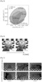
- Applicants simulated the visual appearances of coatings applied to a spherical object by varying the thickness h from a bidirectional reflectance distribution function (BRDF) model. They found that as the thickness h of the second layer increased, bright and diffuse colors appeared from a pale bluish gray due to changes in the scattering spectra and scattering patterns shown in the figures 4 And 5 .
- BRDF bidirectional reflectance distribution function
- the color due to the silver nanoparticles is pale bluish gray.
- areas of bright colors appear which are represented by dark areas.
- Applicants also note that the visual appearance of a non-spherical object coated with a second layer of non-zero thickness varies depending on the direction of incident light and the direction of observation, thereby giving a "diffuse iridescence" effect.
- the applicants note that two diffuse colours green and violet are generated. The first appears for small angles of incidence and the second for large angles of incidence.
- the presence of the nanoparticles randomly dispersed on the surface of the second layer combined with a finite thickness of the second layer makes it possible to obtain two different colours on the same object.
- Such a visual effect cannot be generated with the solutions of the state of the art which are mainly based on multilayer structures which produce only interferences related to the interfaces.
- the nanostructured surface coating comprises a first layer comprising a random distribution of nanoparticles and a substrate, the first layer being arranged on the substrate.
- the first layer is formed only of nanoparticles without the protective layer.
- the first layer is formed of nanoparticles incorporated in a protective layer.
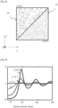
- the nanostructure generates new visual appearances when the degree of correlation p satisfies the following relationship: ⁇ R excl 2 ⁇ p ⁇ 0.69.
- the upper limit 0.69 is the limit beyond which the nanoparticles are no longer considered a disordered system since they form small periodic clusters.
- the system can be considered a periodic system.
- FIG. 9 shows the structural factor S calculated for different degrees of correlation as a function of the scattering wave vector in the q ⁇ plane.
- the curves show that the structural correlation S can suppress or enhance scattering.
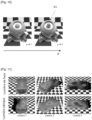
- FIG 10 shows the simulated visual appearances of two spheres coated with a nanostructured surface coating for different degrees of correlation.
- the generated colors always follow the specular direction. Dark regions always appear when the viewing angle and the specular direction are the same.
- the nanostructured surface coating of the present invention can generate new visual appearances by controlling the thickness h of the particle-supporting layer, the distance between two particles d and the degree of structural correlation p on the wavelength scale of the visible spectrum.
- Such a nanostructured surface coating can be used in various industrial fields in which the visual appearance is essential in order to make the object more aesthetic while freeing itself from technical constraints, such as the automobile industry, the cosmetics field, the packaging industry, printing.
Landscapes
- Physics & Mathematics (AREA)
- General Physics & Mathematics (AREA)
- Optics & Photonics (AREA)
- Engineering & Computer Science (AREA)
- Mechanical Engineering (AREA)
- Paints Or Removers (AREA)
- Laminated Bodies (AREA)
- Surface Treatment Of Glass (AREA)
- Silicon Compounds (AREA)
Claims (10)
- Nanostrukturierte Oberflächenbeschichtung (1), welche dazu ausgebildet ist, visuelle Erscheinungen in einem sichtbaren Spektralband zu erzeugen, wobei die Beschichtung umfasst:- eine erste Schicht mit einer Zufallsverteilung von Nanopartikeln (2),- ein Substrat (3), auf dem die erste Schicht angeordnet ist,- wobei die Nanopartikel einen optischen Brechungsindex npart mit einem Wert aufweisen, der dazu geeignet ist, das einfallende Licht jeweils einzeln zu streuen,
wobei die Beschichtung dadurch gekennzeichnet ist, dass- die Nanopartikel derart angeordnet sind, dass der mittlere Abstand zwischen zwei benachbarten Partikeln d gemäß der folgenden Beziehung definiert ist, um eine Interferenz zwischen dem von den Partikeln gestreuten Licht zu erzeugen: R: ist der kleinste geometrische Radius eines Kreises, der den Partikel einschließt,λ: ist die größte Wellenlänge im sichtbaren Spektrum,np: ist der optische Brechungsindex des Mediums der ersten Schicht, in der die Nanopartikel dispergiert sind.
 - Nanostrukturierte Oberflächenbeschichtung nach Anspruch 1, ferner umfassend eine zweite Schicht (30), die zwischen dem Substrat (40) und der ersten Schicht Nanopartikel angeordnet ist:- wobei die zweite Schicht (30) eine Dicke h aufweist, die kleiner oder gleich der größten Wellenlänge des Spektralbandes in der zweiten Schicht ist:
0 ≤ h ≤ max (λ/np), wobei nsup der Brechungsindex der zweiten Schicht ist. - Nanostrukturierte Oberflächenbeschichtung nach Anspruch 2, wobei die zweite Schicht aus einem Material gefertigt ist, dessen Brechungsindex zwischen 1,3 und 2 liegt und das aus den folgenden Materialien gewählt ist: SiOz, SoI-GeI, TiO2, Sl3N4, Polymere und Oxide.
- Nanostrukturierte Oberflächenbeschichtung nach einem der Ansprüche 1 bis 3, wobei das Substrat aus einem Material besteht, dessen Brechungsindex zwischen 1,3 und 4 liegt und das aus den folgenden Materialien gewählt ist: Si, AsGa, Quarz, Siliziumdioxid, Polymere.
- Nanostrukturierte Oberflächenbeschichtung nach einem der Ansprüche 1 bis 4, wobei das Material, das die erste Schicht bildet, in der die Nanopartikel dispergiert sind, einen Brechungsindex np zwischen 1 und 2 aufweist, wobei np derart gewählt ist, dass es kleiner ist als der Brechungsindex der Nanopartikel.
- Nanostrukturierte Oberflächenbeschichtung nach einem der Ansprüche 1 bis 5, wobei die Nanopartikel derart angeordnet sind, dass der Korrelationsgrad p zwischen den Partikeln gemäß der folgenden Beziehung gesteuert wird:
 wobei p durch folgende Beziehung definiert ist: ρπR2 excl, wobei Rexcl der Ausschlussradius ist, der einen Raum um den Nanopartikel definiert, der die Anwesenheit eines anderen Nanopartikels ausschließt,R: ist der kleinste geometrische Radius eines Kreises, der den Partikel einschließt,p: ist die Flächendichte einer Gruppe von Partikeln, die durch die Beziehung 1/d2 definiert ist, wobei d der mittlere Abstand zwischen zwei Massenzentren der Partikel ist, die die nächsten Nachbarn sind.
 - Nanostrukturierte Oberflächenbeschichtung nach einem der Ansprüche 1 bis 6, wobei die Nanopartikel aus einem Material mit einem Brechungsindex von 1,4 oder mehr hergestellt sind.
- Nanostrukturierte Oberflächenbeschichtung nach Anspruch 7, wobei die Nanopartikel aus einem dielektrischen oder metallischen Material hergestellt sind, das aus einem der folgenden Materialien gewählt ist: Silber, Gold, Aluminium, Silizium, Germanium, Titandioxid, Polymer, Siliziumnitrid.
- Nanostrukturierte Oberflächenbeschichtung nach einem der Ansprüche 1 bis 8, wobei die Nanopartikel eine zylindrische Form, eine Kugelform, eine kubische Form oder eine andere geometrische Form aufweisen.
- Nanostrukturierte Oberflächenbeschichtung nach einem der vorhergehenden Ansprüche, wobei die Nanopartikel einen Flächenfüllgrad f zwischen 5 und 30 % aufweisen.
Applications Claiming Priority (2)
| Application Number | Priority Date | Filing Date | Title |
|---|---|---|---|
| FR2100948A FR3119385B1 (fr) | 2021-02-01 | 2021-02-01 | Revêtement de surface nanostructurée pour générer des nouvelles apparences visuelles |
| PCT/FR2022/050123 WO2022162297A1 (fr) | 2021-02-01 | 2022-01-24 | Revetement de surface nanostructuree pour generer des nouvelles apparences visuelles |
Publications (3)
| Publication Number | Publication Date |
|---|---|
| EP4284625A1 EP4284625A1 (de) | 2023-12-06 |
| EP4284625B1 true EP4284625B1 (de) | 2024-11-13 |
| EP4284625C0 EP4284625C0 (de) | 2024-11-13 |
Family
ID=76034695
Family Applications (1)
| Application Number | Title | Priority Date | Filing Date |
|---|---|---|---|
| EP22705434.3A Active EP4284625B1 (de) | 2021-02-01 | 2022-01-24 | Nanostrukturierte oberflächenbeschichtung zur erzeugung neuartiger visueller erscheinungen |
Country Status (4)
| Country | Link |
|---|---|
| US (1) | US20240085598A1 (de) |
| EP (1) | EP4284625B1 (de) |
| FR (1) | FR3119385B1 (de) |
| WO (1) | WO2022162297A1 (de) |
Family Cites Families (3)
| Publication number | Priority date | Publication date | Assignee | Title |
|---|---|---|---|---|
| FR3062348B1 (fr) * | 2017-01-31 | 2019-03-22 | Peugeot Citroen Automobiles Sa | Planche de bord d’un vehicule, notamment automobile |
| FR3073321B1 (fr) * | 2017-11-07 | 2019-12-20 | Commissariat A L'energie Atomique Et Aux Energies Alternatives | Procede de cristallisation d'une couche utile |
| WO2020018906A1 (en) * | 2018-07-20 | 2020-01-23 | Nanoclear Technologies Inc. | Control of light scattering with nanoparticles and/or coatings |
-
2021
- 2021-02-01 FR FR2100948A patent/FR3119385B1/fr active Active
-
2022
- 2022-01-24 EP EP22705434.3A patent/EP4284625B1/de active Active
- 2022-01-24 WO PCT/FR2022/050123 patent/WO2022162297A1/fr not_active Ceased
- 2022-01-24 US US18/263,620 patent/US20240085598A1/en active Pending
Also Published As
| Publication number | Publication date |
|---|---|
| US20240085598A1 (en) | 2024-03-14 |
| FR3119385A1 (fr) | 2022-08-05 |
| EP4284625C0 (de) | 2024-11-13 |
| WO2022162297A1 (fr) | 2022-08-04 |
| EP4284625A1 (de) | 2023-12-06 |
| FR3119385B1 (fr) | 2023-01-13 |
Similar Documents
| Publication | Publication Date | Title |
|---|---|---|
| JP6729396B2 (ja) | 光学装置および光学部材 | |
| CN104136944B (zh) | 用于防伪纸、有价文件或类似物的防伪元件 | |
| EP0408445B1 (de) | Optische Vorrichtung zur Bildvergrösserung | |
| EP3203316B1 (de) | Anzeigesystem eines bildes auf einer windschutzscheibe | |
| WO2018138223A1 (fr) | Détecteur optique de particules | |
| EP3007903B1 (de) | Sicherheitsstruktur mit einem diffraktiven optischen element | |
| FR3019259A1 (fr) | Guide de lumiere comportant un bandeau en matiere diffusante | |
| EP4284625B1 (de) | Nanostrukturierte oberflächenbeschichtung zur erzeugung neuartiger visueller erscheinungen | |
| EP3052986B1 (de) | Anzeigevorrichtung mit rückprojektion | |
| EP3285118B1 (de) | Bildschirm, der mit rückstrahlenden mikrostrukturen ausgestattet ist | |
| EP3192645B1 (de) | Herstellungsverfahren eines bildschirms, der mit rückstrahlenden mikrostrukturen ausgestattet ist | |
| EP3203305A1 (de) | Optisches system zur einfachen bündelung für kohärente leuchtquelle | |
| EP4078020A1 (de) | System zum projizieren eines lichtstrahls | |
| EP2927570B1 (de) | Lichtwellenleiter, der eine austrittsoberfläche umfasst, die mit lichtstreuendem material bedeckt ist | |
| WO2020128105A1 (fr) | Détecteur optique de particules | |
| EP4075182B1 (de) | Optischer scanner | |
| FR3124980A1 (fr) | Composants optiques de sécurité, fabrication de tels composants et documents sécurisés équipés de tels composants | |
| EP3798695A1 (de) | Diffuse struktur für lichtquelle | |
| OA13016A (fr) | Dipositif de sécurité en guide d'onde. | |
| FR3049071A1 (fr) | Dispositif d’affichage a composant optique a reflexion selective et elements optiques de deflexion et de focalisation, pour un vehicule | |
| FR3102567A1 (fr) | Dispositif optique | |
| EP2981807B1 (de) | Optisches verfahren zur charakterisierung einer lichtbrechenden oberfläche und vorrichtung zur durchführung solch eines verfahrens | |
| FR3010000A1 (de) | ||
| WO2025252831A1 (fr) | Module réfléchissant rouge pour pièce automobile, et système associé | |
| WO2024223226A1 (fr) | Composants optiques de sécurité, fabrication de tels composants et objets sécurisés équipés de tels composants |
Legal Events
| Date | Code | Title | Description |
|---|---|---|---|
| STAA | Information on the status of an ep patent application or granted ep patent |
Free format text: STATUS: UNKNOWN |
|
| STAA | Information on the status of an ep patent application or granted ep patent |
Free format text: STATUS: THE INTERNATIONAL PUBLICATION HAS BEEN MADE |
|
| PUAI | Public reference made under article 153(3) epc to a published international application that has entered the european phase |
Free format text: ORIGINAL CODE: 0009012 |
|
| STAA | Information on the status of an ep patent application or granted ep patent |
Free format text: STATUS: REQUEST FOR EXAMINATION WAS MADE |
|
| 17P | Request for examination filed |
Effective date: 20230802 |
|
| AK | Designated contracting states |
Kind code of ref document: A1 Designated state(s): AL AT BE BG CH CY CZ DE DK EE ES FI FR GB GR HR HU IE IS IT LI LT LU LV MC MK MT NL NO PL PT RO RS SE SI SK SM TR |
|
| DAV | Request for validation of the european patent (deleted) | ||
| DAX | Request for extension of the european patent (deleted) | ||
| GRAP | Despatch of communication of intention to grant a patent |
Free format text: ORIGINAL CODE: EPIDOSNIGR1 |
|
| STAA | Information on the status of an ep patent application or granted ep patent |
Free format text: STATUS: GRANT OF PATENT IS INTENDED |
|
| INTG | Intention to grant announced |
Effective date: 20240605 |
|
| GRAS | Grant fee paid |
Free format text: ORIGINAL CODE: EPIDOSNIGR3 |
|
| GRAA | (expected) grant |
Free format text: ORIGINAL CODE: 0009210 |
|
| STAA | Information on the status of an ep patent application or granted ep patent |
Free format text: STATUS: THE PATENT HAS BEEN GRANTED |
|
| AK | Designated contracting states |
Kind code of ref document: B1 Designated state(s): AL AT BE BG CH CY CZ DE DK EE ES FI FR GB GR HR HU IE IS IT LI LT LU LV MC MK MT NL NO PL PT RO RS SE SI SK SM TR |
|
| REG | Reference to a national code |
Ref country code: GB Ref legal event code: FG4D Free format text: NOT ENGLISH |
|
| REG | Reference to a national code |
Ref country code: CH Ref legal event code: EP |
|
| REG | Reference to a national code |
Ref country code: IE Ref legal event code: FG4D Free format text: LANGUAGE OF EP DOCUMENT: FRENCH |
|
| REG | Reference to a national code |
Ref country code: DE Ref legal event code: R096 Ref document number: 602022007721 Country of ref document: DE |
|
| U01 | Request for unitary effect filed |
Effective date: 20241122 |
|
| U07 | Unitary effect registered |
Designated state(s): AT BE BG DE DK EE FI FR IT LT LU LV MT NL PT RO SE SI Effective date: 20241128 |
|
| U20 | Renewal fee for the european patent with unitary effect paid |
Year of fee payment: 4 Effective date: 20250217 |
|
| PG25 | Lapsed in a contracting state [announced via postgrant information from national office to epo] |
Ref country code: HR Free format text: LAPSE BECAUSE OF FAILURE TO SUBMIT A TRANSLATION OF THE DESCRIPTION OR TO PAY THE FEE WITHIN THE PRESCRIBED TIME-LIMIT Effective date: 20241113 Ref country code: IS Free format text: LAPSE BECAUSE OF FAILURE TO SUBMIT A TRANSLATION OF THE DESCRIPTION OR TO PAY THE FEE WITHIN THE PRESCRIBED TIME-LIMIT Effective date: 20250313 |
|
| PG25 | Lapsed in a contracting state [announced via postgrant information from national office to epo] |
Ref country code: ES Free format text: LAPSE BECAUSE OF FAILURE TO SUBMIT A TRANSLATION OF THE DESCRIPTION OR TO PAY THE FEE WITHIN THE PRESCRIBED TIME-LIMIT Effective date: 20241113 |
|
| PG25 | Lapsed in a contracting state [announced via postgrant information from national office to epo] |
Ref country code: NO Free format text: LAPSE BECAUSE OF FAILURE TO SUBMIT A TRANSLATION OF THE DESCRIPTION OR TO PAY THE FEE WITHIN THE PRESCRIBED TIME-LIMIT Effective date: 20250213 |
|
| PG25 | Lapsed in a contracting state [announced via postgrant information from national office to epo] |
Ref country code: GR Free format text: LAPSE BECAUSE OF FAILURE TO SUBMIT A TRANSLATION OF THE DESCRIPTION OR TO PAY THE FEE WITHIN THE PRESCRIBED TIME-LIMIT Effective date: 20250214 |
|
| PG25 | Lapsed in a contracting state [announced via postgrant information from national office to epo] |
Ref country code: PL Free format text: LAPSE BECAUSE OF FAILURE TO SUBMIT A TRANSLATION OF THE DESCRIPTION OR TO PAY THE FEE WITHIN THE PRESCRIBED TIME-LIMIT Effective date: 20241113 |
|
| PG25 | Lapsed in a contracting state [announced via postgrant information from national office to epo] |
Ref country code: RS Free format text: LAPSE BECAUSE OF FAILURE TO SUBMIT A TRANSLATION OF THE DESCRIPTION OR TO PAY THE FEE WITHIN THE PRESCRIBED TIME-LIMIT Effective date: 20250213 |
|
| PG25 | Lapsed in a contracting state [announced via postgrant information from national office to epo] |
Ref country code: SM Free format text: LAPSE BECAUSE OF FAILURE TO SUBMIT A TRANSLATION OF THE DESCRIPTION OR TO PAY THE FEE WITHIN THE PRESCRIBED TIME-LIMIT Effective date: 20241113 |
|
| PG25 | Lapsed in a contracting state [announced via postgrant information from national office to epo] |
Ref country code: SK Free format text: LAPSE BECAUSE OF FAILURE TO SUBMIT A TRANSLATION OF THE DESCRIPTION OR TO PAY THE FEE WITHIN THE PRESCRIBED TIME-LIMIT Effective date: 20241113 |
|
| PG25 | Lapsed in a contracting state [announced via postgrant information from national office to epo] |
Ref country code: CZ Free format text: LAPSE BECAUSE OF FAILURE TO SUBMIT A TRANSLATION OF THE DESCRIPTION OR TO PAY THE FEE WITHIN THE PRESCRIBED TIME-LIMIT Effective date: 20241113 |
|
| REG | Reference to a national code |
Ref country code: CH Ref legal event code: PL |
|
| PG25 | Lapsed in a contracting state [announced via postgrant information from national office to epo] |
Ref country code: MC Free format text: LAPSE BECAUSE OF FAILURE TO SUBMIT A TRANSLATION OF THE DESCRIPTION OR TO PAY THE FEE WITHIN THE PRESCRIBED TIME-LIMIT Effective date: 20241113 |
|
| PLBE | No opposition filed within time limit |
Free format text: ORIGINAL CODE: 0009261 |
|
| STAA | Information on the status of an ep patent application or granted ep patent |
Free format text: STATUS: NO OPPOSITION FILED WITHIN TIME LIMIT |
|
| PG25 | Lapsed in a contracting state [announced via postgrant information from national office to epo] |
Ref country code: CH Free format text: LAPSE BECAUSE OF NON-PAYMENT OF DUE FEES Effective date: 20250131 |
|
| 26N | No opposition filed |
Effective date: 20250814 |