EP4283642A1 - Circuit board - Google Patents
Circuit board Download PDFInfo
- Publication number
- EP4283642A1 EP4283642A1 EP22742462.9A EP22742462A EP4283642A1 EP 4283642 A1 EP4283642 A1 EP 4283642A1 EP 22742462 A EP22742462 A EP 22742462A EP 4283642 A1 EP4283642 A1 EP 4283642A1
- Authority
- EP
- European Patent Office
- Prior art keywords
- capacitor
- thin film
- circuit board
- dielectric layer
- film capacitor
- Prior art date
- Legal status (The legal status is an assumption and is not a legal conclusion. Google has not performed a legal analysis and makes no representation as to the accuracy of the status listed.)
- Pending
Links
Images








Classifications
-
- H—ELECTRICITY
- H01—ELECTRIC ELEMENTS
- H01G—CAPACITORS; CAPACITORS, RECTIFIERS, DETECTORS, SWITCHING DEVICES, LIGHT-SENSITIVE OR TEMPERATURE-SENSITIVE DEVICES OF THE ELECTROLYTIC TYPE
- H01G2/00—Details of capacitors not covered by a single one of groups H01G4/00-H01G11/00
- H01G2/02—Mountings
- H01G2/06—Mountings specially adapted for mounting on a printed-circuit support
-
- H—ELECTRICITY
- H05—ELECTRIC TECHNIQUES NOT OTHERWISE PROVIDED FOR
- H05K—PRINTED CIRCUITS; CASINGS OR CONSTRUCTIONAL DETAILS OF ELECTRIC APPARATUS; MANUFACTURE OF ASSEMBLAGES OF ELECTRICAL COMPONENTS
- H05K1/00—Printed circuits
- H05K1/18—Printed circuits structurally associated with non-printed electric components
- H05K1/181—Printed circuits structurally associated with non-printed electric components associated with surface mounted components
-
- H—ELECTRICITY
- H01—ELECTRIC ELEMENTS
- H01G—CAPACITORS; CAPACITORS, RECTIFIERS, DETECTORS, SWITCHING DEVICES, LIGHT-SENSITIVE OR TEMPERATURE-SENSITIVE DEVICES OF THE ELECTROLYTIC TYPE
- H01G4/00—Fixed capacitors; Processes of their manufacture
- H01G4/002—Details
- H01G4/228—Terminals
-
- H—ELECTRICITY
- H01—ELECTRIC ELEMENTS
- H01G—CAPACITORS; CAPACITORS, RECTIFIERS, DETECTORS, SWITCHING DEVICES, LIGHT-SENSITIVE OR TEMPERATURE-SENSITIVE DEVICES OF THE ELECTROLYTIC TYPE
- H01G4/00—Fixed capacitors; Processes of their manufacture
- H01G4/002—Details
- H01G4/228—Terminals
- H01G4/252—Terminals the terminals being coated on the capacitive element
-
- H—ELECTRICITY
- H01—ELECTRIC ELEMENTS
- H01G—CAPACITORS; CAPACITORS, RECTIFIERS, DETECTORS, SWITCHING DEVICES, LIGHT-SENSITIVE OR TEMPERATURE-SENSITIVE DEVICES OF THE ELECTROLYTIC TYPE
- H01G4/00—Fixed capacitors; Processes of their manufacture
- H01G4/33—Thin- or thick-film capacitors (thin- or thick-film circuits; capacitors without a potential-jump or surface barrier specially adapted for integrated circuits, details thereof, multistep manufacturing processes therefor)
-
- H—ELECTRICITY
- H01—ELECTRIC ELEMENTS
- H01G—CAPACITORS; CAPACITORS, RECTIFIERS, DETECTORS, SWITCHING DEVICES, LIGHT-SENSITIVE OR TEMPERATURE-SENSITIVE DEVICES OF THE ELECTROLYTIC TYPE
- H01G4/00—Fixed capacitors; Processes of their manufacture
- H01G4/40—Structural combinations of fixed capacitors with other electric elements, the structure mainly consisting of a capacitor, e.g. RC combinations
-
- H—ELECTRICITY
- H05—ELECTRIC TECHNIQUES NOT OTHERWISE PROVIDED FOR
- H05K—PRINTED CIRCUITS; CASINGS OR CONSTRUCTIONAL DETAILS OF ELECTRIC APPARATUS; MANUFACTURE OF ASSEMBLAGES OF ELECTRICAL COMPONENTS
- H05K1/00—Printed circuits
- H05K1/02—Details
- H05K1/0201—Thermal arrangements, e.g. for cooling, heating or preventing overheating
- H05K1/0203—Cooling of mounted components
- H05K1/0204—Cooling of mounted components using means for thermal conduction connection in the thickness direction of the substrate
-
- H—ELECTRICITY
- H05—ELECTRIC TECHNIQUES NOT OTHERWISE PROVIDED FOR
- H05K—PRINTED CIRCUITS; CASINGS OR CONSTRUCTIONAL DETAILS OF ELECTRIC APPARATUS; MANUFACTURE OF ASSEMBLAGES OF ELECTRICAL COMPONENTS
- H05K1/00—Printed circuits
- H05K1/02—Details
- H05K1/0201—Thermal arrangements, e.g. for cooling, heating or preventing overheating
- H05K1/0203—Cooling of mounted components
- H05K1/0209—External configuration of printed circuit board adapted for heat dissipation, e.g. lay-out of conductors, coatings
-
- H—ELECTRICITY
- H05—ELECTRIC TECHNIQUES NOT OTHERWISE PROVIDED FOR
- H05K—PRINTED CIRCUITS; CASINGS OR CONSTRUCTIONAL DETAILS OF ELECTRIC APPARATUS; MANUFACTURE OF ASSEMBLAGES OF ELECTRICAL COMPONENTS
- H05K1/00—Printed circuits
- H05K1/02—Details
- H05K1/03—Use of materials for the substrate
- H05K1/0306—Inorganic insulating substrates, e.g. ceramic, glass
-
- H—ELECTRICITY
- H05—ELECTRIC TECHNIQUES NOT OTHERWISE PROVIDED FOR
- H05K—PRINTED CIRCUITS; CASINGS OR CONSTRUCTIONAL DETAILS OF ELECTRIC APPARATUS; MANUFACTURE OF ASSEMBLAGES OF ELECTRICAL COMPONENTS
- H05K1/00—Printed circuits
- H05K1/02—Details
- H05K1/11—Printed elements for providing electric connections to or between printed circuits
- H05K1/111—Pads for surface mounting, e.g. lay-out
-
- H—ELECTRICITY
- H05—ELECTRIC TECHNIQUES NOT OTHERWISE PROVIDED FOR
- H05K—PRINTED CIRCUITS; CASINGS OR CONSTRUCTIONAL DETAILS OF ELECTRIC APPARATUS; MANUFACTURE OF ASSEMBLAGES OF ELECTRICAL COMPONENTS
- H05K1/00—Printed circuits
- H05K1/02—Details
- H05K1/11—Printed elements for providing electric connections to or between printed circuits
- H05K1/111—Pads for surface mounting, e.g. lay-out
- H05K1/112—Pads for surface mounting, e.g. lay-out directly combined with via connections
-
- H—ELECTRICITY
- H05—ELECTRIC TECHNIQUES NOT OTHERWISE PROVIDED FOR
- H05K—PRINTED CIRCUITS; CASINGS OR CONSTRUCTIONAL DETAILS OF ELECTRIC APPARATUS; MANUFACTURE OF ASSEMBLAGES OF ELECTRICAL COMPONENTS
- H05K1/00—Printed circuits
- H05K1/16—Printed circuits incorporating printed electric components, e.g. printed resistors, capacitors or inductors
- H05K1/162—Printed circuits incorporating printed electric components, e.g. printed resistors, capacitors or inductors incorporating printed capacitors
-
- H—ELECTRICITY
- H05—ELECTRIC TECHNIQUES NOT OTHERWISE PROVIDED FOR
- H05K—PRINTED CIRCUITS; CASINGS OR CONSTRUCTIONAL DETAILS OF ELECTRIC APPARATUS; MANUFACTURE OF ASSEMBLAGES OF ELECTRICAL COMPONENTS
- H05K2201/00—Indexing scheme relating to printed circuits covered by H05K1/00
- H05K2201/06—Thermal details
- H05K2201/066—Heatsink mounted on the surface of the printed circuit board [PCB]
-
- H—ELECTRICITY
- H05—ELECTRIC TECHNIQUES NOT OTHERWISE PROVIDED FOR
- H05K—PRINTED CIRCUITS; CASINGS OR CONSTRUCTIONAL DETAILS OF ELECTRIC APPARATUS; MANUFACTURE OF ASSEMBLAGES OF ELECTRICAL COMPONENTS
- H05K2201/00—Indexing scheme relating to printed circuits covered by H05K1/00
- H05K2201/10—Details of components or other objects attached to or integrated in a printed circuit board
- H05K2201/10007—Types of components
- H05K2201/10015—Non-printed capacitor
Definitions
- the present invention relates to a circuit board and, more particularly, to a circuit board having a configuration in which a thin film capacitor is mounted on a substrate having a ceramic board as a base material.
- Patent Document 1 discloses a circuit board having a structure in which a chip capacitor is mounted on a DBC (Direct Bonded Copper) substrate.
- the DBC substrate uses a ceramic board as a base material and thus has much higher heat dissipation characteristics than typical printed circuit boards using a resin material.
- circuit board described in Patent Document 1 uses a typical chip capacitor, and thus sufficient heat dissipation characteristics of heat generated by the chip capacitor cannot be achieved.
- a circuit board includes: a substrate including a ceramic board, a first conductor layer formed on one surface of the ceramic board, and a second conductor layer formed on the other surface of the ceramic board; and a thin film capacitor mounted on the substrate such that a mounting surface thereof faces the first conductor layer.
- the first conductor layer includes a first wiring pattern.
- the thin film capacitor includes a dielectric layer, a first capacitor electrode formed on one surface of the dielectric layer, and a second capacitor electrode formed on the other surface of the dielectric layer. The first capacitor electrode is connected to the first wiring pattern, and the second capacitor electrode or a terminal electrode connected thereto is exposed to the upper surface of the thin film capacitor that faces away from the mounting surface.
- the thin film capacitor is mounted on the substrate having the ceramic board as a base material, and the second capacitor electrode of the thin film capacitor or the terminal electrode connected thereto is exposed to the upper surface of the thin film capacitor, thus allowing high heat dissipation characteristics to be obtained.
- the exposed area of the second capacitor electrode or terminal electrode may be larger than the area of the first capacitor electrode. This further enhances heat dissipation characteristics through the second capacitor electrode or terminal electrode.
- the first conductor layer may further include a second wiring pattern, and the second capacitor electrode may be connected to the second wiring pattern. This allows the thin film capacitor to be surface-mounted on the substrate.
- the first conductor layer may further include a second wiring pattern
- the thin film capacitor may further include a third capacitor electrode formed on one surface of the dielectric layer
- the third capacitor electrode may be connected to the second wiring pattern.
- the circuit board according to the present invention may further include a semiconductor device mounted on one surface of the substrate, and the second capacitor electrode of the thin film capacitor or the terminal electrode and the semiconductor device may be connected to each other through a bonding wire. This allows the semiconductor device and the thin film capacitor to be directly connected. In this case, the semiconductor device and the thin film capacitor may be connected through a plurality of bonding wires. This increases connection reliability.
- circuit board capable of achieving improved heat dissipation characteristics.
- FIG. 1 is a schematic cross-sectional view for explaining the configuration of a circuit board 1 according to a first embodiment of the present invention.
- the circuit board 1 includes a substrate 10 and a thin film capacitor 20 mounted on the substrate 10.
- the substrate 10 includes a ceramic board 11 as a base material, a conductor layer 12 formed on one surface 11a of the ceramic board 11, and a conductor layer 13 formed on the other surface 11b of the ceramic board 11.
- a metal oxide or a metal nitride such as Al 2 O 3 , AlN, or Si 3 N 4 can be used.
- a good conductor such as Cu or Al can be used.
- the substrate 10 constitutes a DBC (Direct Bonded Copper) substrate
- DBA Direct Bonded Aluminum
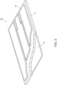
- FIG. 2 is a schematic perspective view for explaining the structure of the substrate 10.
- the conductor layer 12 has a plurality of wiring patterns, while the conductor layer 13 is a solid pattern.
- the conductor layer 13 is fixed to a not-shown metal heat sink or the like.
- the conductor layer 12 includes wiring patterns 12a and 12b.
- FIG. 3 is a schematic cross-sectional view for explaining the configuration of the thin film capacitor 20.
- the thin film capacitor 20 includes a dielectric layer 21, a capacitor electrode 22 formed on one surface 21a of the dielectric layer 21, a capacitor electrode 23 formed on the other surface 21b of the dielectric layer 21, and a passivation layer 24 provided so as to embed therein the dielectric layer 21 and capacitor electrode 22.
- the capacitor electrodes 22 and 23 overlap each other with the dielectric layer 21 interposed therebetween, whereby a predetermined capacitance can be obtained.
- the dielectric layer 21 is formed using, for example, a perovskite dielectric material.
- the perovskite dielectric material include: a ferroelectric or paraelectric material having a perovskite structure such as BaTiO 3 (barium titanate), (Ba 1-x Sr x )TiO 3 (barium strontium titanate), (Ba 1-X Ca X )TiO 3 , PbTiO 3 , Pb (Zr X Ti 1-X )O 3 , (Sr 1-x Ca x )(Ti 1-y Zr y )O 3 , or Ba(Mg 1/3 Ta 2/3 )O 3 ; a complex perovskite relaxer ferroelectric material such as Pb(Mg 1/3 Nb 2/3 )O 3 ; a bismuth layered compound such as Bi 4 Ti 3 O 12 or SrBi 2 Ta 2 O 9 ; and a tungsten bronze ferroelectric material such as (Sr 1-X Ba X )
- a ratio of A site and B site in the perovskite structure, perovskite relaxer ferroelectric material, bismuth layered compound, and tungsten bronze ferroelectric material is typically an integral ratio; however, it is allowable to intentionally depart the ratio from the integral ratio to improve characteristics.
- An additive can be appropriately added to the dielectric layer 21 as an accessory component to control the characteristics of the dielectric layer 21.
- the relative permittivity ( ⁇ r ) of the dielectric layer 21 is, for example, equal to or more than 10.
- the relative permittivity of the dielectric layer 21 is preferably as large as possible, and the upper limit value thereof is not particularly limited. Further, the withstand voltage of the dielectric layer 21 is also as large as possible, and the upper limit value thereof is not particularly limited.
- the thickness of the dielectric layer 21 is, e.g., about 10 nm to 6000 nm.
- the capacitor electrodes 22 and 23 are each a metal foil made of high melting point metal such as nickel (Ni).
- the capacitor electrode 23 functions also as a support for ensuring mechanical strength of the thin film capacitor 20.
- the surface of the capacitor electrode 23 facing away from the surface thereof in contact with the dielectric layer 21 constitutes an upper surface 20b of the thin film capacitor 20.
- the dielectric layer 21 and capacitor electrode 22 are stacked in this order on the surface of the capacitor electrode 23 serving as a support.
- the area of the dielectric layer 21 is smaller than the area of the capacitor electrode 23, and the area of the capacitor electrode 22 is smaller than the area of the dielectric layer 21.
- the surface of the passivation layer 24 constitutes a mounting surface 20a of the thin film capacitor 20.
- the passivation layer 24 is made of, for example, resin.
- terminal electrodes 25 and 26 on the mounting surface 20a of the thin film capacitor 20.
- the terminal electrode 25 is connected to the thin film capacitor 20 through a via conductor 25a penetrating the passivation layer 24.
- the dielectric layer 21 and capacitor electrode 22 have an opening 27.
- the terminal electrode 26 is connected to the capacitor electrode 23 through a via conductor 26a penetrating the passivation layer 24 so as to pass the opening 27.
- a configuration in which one capacitor is connected between the terminal electrodes 25 and 26 is obtained.
- a good conductor such as Cu can be used as a material of the terminal electrodes 25, 26 and via conductors 25a, 26a.
- the surfaces of each of the terminal electrodes 25 and 26 may be covered with a surface treated layer such as an ENEPIG film.
- the thus configured thin film capacitor 20 is mounted on the substrate 10 such that the mounting surface 20a faces the conductor layer 12, as illustrated in FIG. 1 .
- the terminal electrode 25 of the thin film capacitor 20 is connected to the wiring pattern 12a
- the terminal electrode 26 of the thin film capacitor 20 is connected to the wiring pattern 12b.
- the connection of the terminal electrodes 25 and 26 to the respective wiring patterns 12a and 12b is made through a solder 28.
- heat generated due to driving of the thin film capacitor 20 under high voltage is not only dissipated to the substrate 10 side through the terminal electrodes 25 and 26 but also dissipated from the upper surface 20b which is the exposed surface of the capacitor electrode 23.
- the back and side surfaces of the capacitor electrode 23 are entirely exposed, and the exposed area of the capacitor electrode 23 is larger than the area of the capacitor electrode 22, thus significantly enhancing heat dissipation characteristics through the capacitor electrode 23.
- MLCC Multilayered Ceramic Capacitors
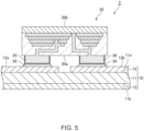
- FIG. 5 is a schematic cross-sectional view for explaining the configuration of a circuit board 2 according to a second embodiment of the present invention.
- the circuit board 2 according to the second embodiment differs from the circuit board 1 according to the first embodiment in that a thin film capacitor 30 is mounted on the substrate 10 in place of the thin film capacitor 20.
- Other basic configurations are the same as those of the circuit board 1 according to the first embodiment, so the same reference numerals are given to the same elements, and overlapping description will be omitted.
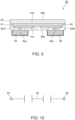
- FIG. 6 is a schematic cross-sectional view for explaining the configuration of the thin film capacitor 30.
- the thin film capacitor 30 includes dielectric layers 31A, 31B, a capacitor electrode 32 positioned between one surface 31Aa of the dielectric layer 31A and one surface 31Ba of the dielectric layer 31B, a capacitor electrode 33A formed on the other surface 31Ab of the dielectric layer 31A, a capacitor electrode 33B formed on the other surface 31Bb of the dielectric layer 31B, and a passivation layer 34 provided so as to embed therein the dielectric layers 31A, 31B and capacitor electrodes 32, 33B.
- the capacitor electrodes 32, 33A, and 33B overlap one another with the dielectric layers 31A and 31B interposed therebetween, whereby a predetermined capacitance can be obtained.
- the material of the dielectric layers 31A and 31B may be the same as that of the above-described dielectric layer 21.
- the material of the capacitor electrodes 32, 33A, and 33B may be the same as that of the above-described capacitor electrodes 22 and 23.
- the capacitor electrode 33A functions also as a support for ensuring mechanical strength of the thin film capacitor 20.
- the surface of the capacitor electrode 33A facing away from the surface thereof in contact with the dielectric layer 31A constitutes an upper surface 30b of the thin film capacitor 30.
- the dielectric layer 31A, capacitor electrode 32, dielectric layer 31B, and capacitor electrode 33B are stacked in this order on the surface of the capacitor electrode 33A serving as a support.
- the area of the dielectric layer 31A is smaller than the area of the capacitor electrode 33A
- the area of the capacitor electrode 32 is smaller than the area of the dielectric layer 31A
- the area of the dielectric layer 31B is smaller than the area of the capacitor electrode 32
- the area of the capacitor electrode 33B is smaller than the area of the dielectric layer 31B.
- the surface of the passivation layer 34 constitutes a mounting surface 30a of the thin film capacitor 30.
- the dielectric layer 31B and capacitor electrode 33B have an opening 37A. Further, the dielectric layer 31A, capacitor electrode 32, dielectric layer 31B, and capacitor electrode 33B have an opening 37B.
- the terminal electrode 35 is connected to the capacitor electrode 32 through a via conductor 35a penetrating the passivation layer 34 so as to pass the opening 37A.
- the terminal electrode 36 is connected to the capacitor electrodes 33A and 33B through a via conductor 36a penetrating the passivation layer 34 so as to pass the opening 37B.
- FIG. 7 a configuration in which two capacitors are connected between the terminal electrodes 35 and 36 is obtained.
- the surfaces of each of the terminal electrodes 35 and 36 may be covered with a surface treated layer such as an ENEPIG film.
- the thus configured thin film capacitor 30 is mounted on the substrate 10 such that the mounting surface 30a faces the conductor layer 12, as illustrated in FIG. 5 .
- the terminal electrode 35 of the thin film capacitor 30 is connected to the wiring pattern 12a
- the terminal electrode 36 of the thin film capacitor 30 is connected to the wiring pattern 12b.
- the connection of the terminal electrodes 35 and 36 to the respective wiring patterns 12a and 12b is made through a solder 38.
- the circuit board 2 according to the present embodiment uses the thin film capacitor 30 having a configuration in which two capacitors are connected in parallel, making it possible to obtain a capacitance larger than that obtained in the circuit board 1 according to the first embodiment.
- the number of capacitors to be connected in parallel is not particularly limited and may be three or more.
- FIG. 8 is a schematic cross-sectional view for explaining the configuration of a circuit board 3 according to a third embodiment of the present invention.
- the circuit board 3 according to the third embodiment differs from the circuit board 1 according to the first embodiment in that a thin film capacitor 40 is mounted, in place of the thin film capacitor 20, on the substrate 10.
- Other basic configurations are the same as those of the circuit board 1 according to the first embodiment, so the same reference numerals are given to the same elements, and overlapping description will be omitted.
- FIG. 9 is a schematic cross-sectional view for explaining the configuration of the thin film capacitor 40.
- the thin film capacitor 40 includes a dielectric layer 41, capacitor electrodes 42A and 42B formed on one surface 41a of the dielectric layer 41, a capacitor electrode 43 formed on the other surface 41b of the dielectric layer 41, and a passivation layer 44 provided so as to embed therein the dielectric layer 41 and capacitor electrodes 42A and 42B.
- the capacitor electrodes 42A and 42B are formed at mutually different plane positions on the one surface 41a of the dielectric layer 41 and each overlap the capacitor electrode 43 with the dielectric layer 41 interposed therebetween.
- the material of the dielectric layer 41 may be the same as that of the above-described dielectric layer 21.
- the material of the capacitor electrodes 42A, 42B, and 43 may be the same as that of the above-described capacitor electrodes 22 and 23.
- the capacitor electrode 43 functions also as a support for ensuring mechanical strength of the thin film capacitor 40.
- the surface of the capacitor electrode 43 facing away from the surface thereof in contact with the dielectric layer 41 constitutes an upper surface 40b of the thin film capacitor 40.
- the dielectric layer 41, capacitor electrodes 42A and 42B are stacked in this order on the surface of the capacitor electrode 43 serving as a support.
- the surface of the passivation layer 44 constitutes a mounting surface 40a of the thin film capacitor 40.
- terminal electrodes 45 and 46 on the mounting surface 40a of the thin film capacitor 40.
- the terminal electrode 45 is connected to the capacitor electrode 42A through a via conductor 45a penetrating the passivation layer 44.
- the terminal electrode 46 is connected to the capacitor electrode 42B through a via conductor 46a penetrating the passivation layer 44.
- FIG. 10 a configuration in which two capacitors are connected in series between the terminal electrodes 45 and 46 is obtained.
- the surfaces of each of the terminal electrodes 45 and 46 may be covered with a surface treated layer such as an ENEPIG film.
- the thus configured thin film capacitor 40 is mounted on the substrate 10 such that the mounting surface 40a faces the conductor layer 12, as illustrated in FIG. 8 .
- the terminal electrode 45 of the thin film capacitor 40 is connected to the wiring pattern 12a
- the terminal electrode 46 of the thin film capacitor 40 is connected to the wiring pattern 12b.
- the connection of the terminal electrodes 45 and 46 to the respective wiring patterns 12a and 12b is made through a solder 48.
- the circuit board 3 according to the present embodiment uses the thin film capacitor 40 having a configuration in which two capacitors are connected in series, so that voltage to be applied to the dielectric layer 41 is dispersed more than in the circuit board 1 according to the first embodiment. This achieves higher withstand voltage than in the circuit board 1 according to the first embodiment.
- the number of capacitors to be connected in series is not particularly limited and may be three or more.
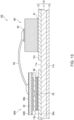
- FIG. 11 is a schematic cross-sectional view for explaining the configuration of a circuit board 4A according to a fourth embodiment of the present invention.
- the circuit board 4A according to the fourth embodiment differs from the circuit board 1 according to the first embodiment in that a thin film capacitor 50A is mounted, in place of the thin film capacitor 20, on the substrate 10 and that a semiconductor device 60 is mounted on the substrate 10.
- Other basic configurations are the same as those of the circuit board 1 according to the first embodiment, so the same reference numerals are given to the same elements, and overlapping description will be omitted.
- the conductor layer 12 of the substrate 10 includes a wiring pattern 12c, and the semiconductor device 60 is mounted on the wiring pattern 12c through a solder 61.
- the semiconductor device 60 is not particularly limited in type and may be a power device of a type in which current flows perpendicular to a semiconductor substrate, such as an IGBT.
- As a material of a semiconductor substrate used for the semiconductor device 60 SiC, GaN, or the like may be used in addition to Si.
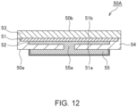
- FIG. 12 is a schematic cross-sectional view for explaining the configuration of the thin film capacitor 50A.
- the thin film capacitor 50A includes a dielectric layer 51, a capacitor electrode 52 formed on one surface 51a of the dielectric layer 51, a capacitor electrode 53 formed on the other surface 51b of the dielectric layer 51, and a passivation layer 54 provided so as to embed therein the dielectric layer 51 and capacitor electrode 52.
- the capacitor electrodes 52 and 53 overlap each other with the dielectric layer 51 interposed therebetween, whereby a predetermined capacitance can be obtained.
- the material of the capacitor electrodes 52 and 53 may be the same as that of the above-described capacitor electrodes 22 and 23. Alternatively, Cu and Ni may be used for the capacitor electrodes 52 and 53, respectively.
- the capacitor electrode 53 functions also as a support for ensuring mechanical strength of the thin film capacitor 50A.
- the surface of the capacitor electrode 53 facing away from the surface thereof in contact with the dielectric layer 51 constitutes an upper surface 50b of the thin film capacitor 50A.
- the dielectric layer 51 and capacitor electrode 52 are stacked in this order on the surface of the capacitor electrode 53 serving as a support.
- the area of the dielectric layer 51 is smaller than the area of the capacitor electrode 53
- the area of the capacitor electrode 52 is smaller than the area of the dielectric layer 51.
- the surface of the passivation layer 54 constitutes a mounting surface 50a of the thin film capacitor 50A.
- terminal electrode 55 on the mounting surface 50a of the thin film capacitor 50A.
- the terminal electrode 55 is connected to the capacitor electrode 52 through a via conductor 55a penetrating the passivation layer 54.
- the surfaces of the terminal electrode 55 may be covered with a surface treated layer such as an ENEPIG film.
- the thus configured thin film capacitor 50A is mounted on the substrate 10 such that the mounting surface 50a faces the conductor layer 12, as illustrated in FIG. 11 .
- the terminal electrode 55 of the thin film capacitor 50A is connected to the wiring pattern 12a through a solder 58.
- the capacitor electrode 53 constituting the upper surface 50b is connected to a bonding pad 62 provided on the upper surface of the semiconductor device 60 through a bonding wire 63 made of Al or the like.
- the thin film capacitor 50A is connected between the wiring pattern 12a and the semiconductor device 60.
- the capacitor electrode 53 constituting the upper surface 50b is used as a bonding pad, allowing the thin film capacitor 50A and semiconductor device 60 to be directly connected without intervention of the substrate 10.
- the capacitor electrode 53 has an area larger than that of the capacitor electrode 52, meaning that the upper surface 50b of the thin film capacitor 50A has a sufficient area, which facilitates bonding work.
- only one terminal electrode 55 is provided on the mounting surface 50a side, so that a sufficient area can be ensured for the terminal electrode 55, which improves heat dissipation characteristics from the thin film capacitor 50A to the substrate 10 through the terminal electrode 55.
- the film thickness of the capacitor electrode 53 may be made larger than those of the capacitor electrodes 23, 33A, and 43 described in the first to third embodiments. This allows the capacitor electrode 53 to function as a heat sink, which improves heat dissipation characteristics and can mitigate damage to be applied to the thin film capacitor 50A at the time of wire bonding.
- FIG. 13 is a schematic cross-sectional view for explaining the configuration of a circuit board 4B according to a modification of the fourth embodiment.
- the circuit board 4B according to the present modification differs from the circuit board 4A according to the fourth embodiment in that a thin film capacitor 50B is mounted, in place of the thin film capacitor 50A, on the substrate 10.
- Other basic configurations are the same as those of the circuit board 4A according to the fourth embodiment, so the same reference numerals are given to the same elements, and overlapping description will be omitted.
- FIG. 14 is a schematic cross-sectional view for explaining the configuration of the thin film capacitor 50B.
- the thin film capacitor 50B differs from the thin film capacitor 50A in that the surface of the capacitor electrode 53 is covered with a metal film 53B made of Sn or the like.
- the metal film 53B functions to reduce surface roughness of the upper surface 50b of the thin film capacitor 50B and enhance adhesion performance of the bonding wire 63.
- a surface roughness Ra of the metal film 53B may be less than 100 nm.
- the surface of the capacitor electrode 53 may not necessarily be exposed and may be covered with the metal film 53B. Instead of covering the surface of the capacitor electrode 53 with the metal film 53B, the surface of the capacitor electrode 53 may be subjected to polishing so as to reduce the surface roughness of the upper surface 50b.
- FIG. 15 is a schematic cross-sectional view for explaining the configuration of a circuit board 5 according to a fifth embodiment of the present invention.
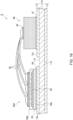
- the circuit board 5 according to the fifth embodiment differs from the circuit board 4A according to the fourth embodiment in that a plurality of the bonding wires 63 are provided juxtaposed.
- Other basic configurations are the same as those of the circuit board 4A according to the fourth embodiment, so the same reference numerals are given to the same elements, and overlapping description will be omitted.
- the thin film capacitor 50A and the semiconductor device 60 are connected by the plurality of bonding wires 63, thus increasing connection reliability and improving heat dissipation characteristics through the bonding wire 63.
- FIG. 16 is a schematic cross-sectional view for explaining the configuration of a circuit board 6 according to a sixth embodiment of the present invention.
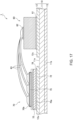
- the circuit board 6 according to the sixth embodiment differs from the circuit board 5 according to the fifth embodiment in that the thin film capacitor 50A is mounted upside down.
- Other basic configurations are the same as those of the circuit board 5 according to the fifth embodiment, so the same reference numerals are given to the same elements, and overlapping description will be omitted.
- the surface of the capacitor electrode 53 constitutes the mounting surface 50a, and the surface of the passivation layer 54 constitutes the upper surface 50b.
- the capacitor electrode 53 is connected to the wiring pattern 12a through the solder 58, and the terminal electrode 55 is connected to the semiconductor device 60 through the plurality of bonding wires 63.
- the thin film capacitor 50A may be mounted upside down on the substrate 10.
- FIG. 17 is a schematic cross-sectional view for explaining the configuration of a circuit board 7 according to a seventh embodiment of the present invention.
- the circuit board 7 according to the seventh embodiment differs from the circuit board 6 according to the sixth embodiment in that a thin film capacitor 70 is mounted, in place of the thin film capacitor 50A, on the substrate 10.
- Other basic configurations are the same as those of the circuit board 6 according to the sixth embodiment, so the same reference numerals are given to the same elements, and overlapping description will be omitted.
- FIG. 18 is a schematic cross-sectional view for explaining the configuration of the thin film capacitor 70.
- the thin film capacitor 70 includes a dielectric layer 71, a capacitor electrode 72 formed on one surface 71a of the dielectric layer 71, a capacitor electrode 73 formed on the other surface 71b of the dielectric layer 71, a passivation layer 74 provided so as to embed therein the dielectric layer 71, and a terminal electrode 75 provided on the surface of the capacitor electrode 73 facing away from the surface thereof in contact with the dielectric layer 71.
- the capacitor electrodes 72 and 73 overlap each other with the dielectric layer 71 interposed therebetween, whereby a predetermined capacitance can be obtained.
- the material of the capacitor electrodes 72 and 73 may be the same as that of the above-described capacitor electrodes 53 and 52.
- the capacitor electrode 72 functions also as a support for ensuring mechanical strength of the thin film capacitor 70.
- the surface of the capacitor electrode 72 facing away from the surface thereof in contact with the dielectric layer 71 constitutes a mounting surface 70a of the thin film capacitor 70.
- the surface of the terminal electrode 75 constitutes an upper surface 70b of the thin film capacitor 70.
- the surfaces of the terminal electrode 75 may be covered with a surface treated layer such as an ENEPIG film.
- the thus configured thin film capacitor 70 is mounted on the substrate 10 such that the mounting surface 70a faces the conductor layer 12, as illustrated in FIG. 17 .
- the capacitor electrode 72 of the thin film capacitor 70 is connected to the wiring pattern 12a through a solder 78.
- the terminal electrode 75 constituting the upper surface 70b is connected to the bonding pad 62 provided on the upper surface of the semiconductor device 60 through the plurality of bonding wires 63.
- the thin film capacitor 70 is connected between the wiring pattern 12a and the semiconductor device 60.
- substantially the entire surface of the capacitor electrode 73 contacts the terminal electrode 75, that is, the contact area therebetween is very large, thereby improving heat dissipation characteristics through the terminal electrode 75.
- substantially the entire surface of the capacitor electrode 73 contacts the terminal electrode 75, so that the terminal electrode 75 can be regarded as a part of the capacitor electrode.
Landscapes
- Engineering & Computer Science (AREA)
- Power Engineering (AREA)
- Microelectronics & Electronic Packaging (AREA)
- Manufacturing & Machinery (AREA)
- Chemical & Material Sciences (AREA)
- Ceramic Engineering (AREA)
- Inorganic Chemistry (AREA)
- Parts Printed On Printed Circuit Boards (AREA)
- Fixed Capacitors And Capacitor Manufacturing Machines (AREA)
Abstract
Description
- The present invention relates to a circuit board and, more particularly, to a circuit board having a configuration in which a thin film capacitor is mounted on a substrate having a ceramic board as a base material.
-
Patent Document 1 discloses a circuit board having a structure in which a chip capacitor is mounted on a DBC (Direct Bonded Copper) substrate. The DBC substrate uses a ceramic board as a base material and thus has much higher heat dissipation characteristics than typical printed circuit boards using a resin material. - [Patent Document 1]
JP-2001-507522 - However, the circuit board described in
Patent Document 1 uses a typical chip capacitor, and thus sufficient heat dissipation characteristics of heat generated by the chip capacitor cannot be achieved. - It is therefore an object of the present invention to provide a circuit board capable of achieving improved heat dissipation characteristics.
- A circuit board according to the present invention includes: a substrate including a ceramic board, a first conductor layer formed on one surface of the ceramic board, and a second conductor layer formed on the other surface of the ceramic board; and a thin film capacitor mounted on the substrate such that a mounting surface thereof faces the first conductor layer. The first conductor layer includes a first wiring pattern. The thin film capacitor includes a dielectric layer, a first capacitor electrode formed on one surface of the dielectric layer, and a second capacitor electrode formed on the other surface of the dielectric layer. The first capacitor electrode is connected to the first wiring pattern, and the second capacitor electrode or a terminal electrode connected thereto is exposed to the upper surface of the thin film capacitor that faces away from the mounting surface.
- According to the present invention, the thin film capacitor is mounted on the substrate having the ceramic board as a base material, and the second capacitor electrode of the thin film capacitor or the terminal electrode connected thereto is exposed to the upper surface of the thin film capacitor, thus allowing high heat dissipation characteristics to be obtained.
- In the present invention, the exposed area of the second capacitor electrode or terminal electrode may be larger than the area of the first capacitor electrode. This further enhances heat dissipation characteristics through the second capacitor electrode or terminal electrode.
- In the present invention, the first conductor layer may further include a second wiring pattern, and the second capacitor electrode may be connected to the second wiring pattern. This allows the thin film capacitor to be surface-mounted on the substrate.
- In the present invention, the first conductor layer may further include a second wiring pattern, the thin film capacitor may further include a third capacitor electrode formed on one surface of the dielectric layer, and the third capacitor electrode may be connected to the second wiring pattern. This achieves a configuration in which two capacitors are connected in series to each other, so that voltage applied to the dielectric layer is dispersed.
- The circuit board according to the present invention may further include a semiconductor device mounted on one surface of the substrate, and the second capacitor electrode of the thin film capacitor or the terminal electrode and the semiconductor device may be connected to each other through a bonding wire. This allows the semiconductor device and the thin film capacitor to be directly connected. In this case, the semiconductor device and the thin film capacitor may be connected through a plurality of bonding wires. This increases connection reliability.
- As described above, according to the present invention, there can be provided a circuit board capable of achieving improved heat dissipation characteristics.
-
-
FIG. 1 is a schematic cross-sectional view for explaining the configuration of acircuit board 1 according to a first embodiment of the present invention. -
FIG. 2 is a schematic perspective view for explaining the structure of thesubstrate 10. -
FIG. 3 is a schematic cross-sectional view for explaining the configuration of thethin film capacitor 20. -
FIG. 4 is an equivalent circuit diagram of thethin film capacitor 20. -
FIG. 5 is a schematic cross-sectional view for explaining the configuration of acircuit board 2 according to a second embodiment of the present invention. -
FIG. 6 is a schematic cross-sectional view for explaining the configuration of thethin film capacitor 30. -
FIG. 7 is an equivalent circuit diagram of thethin film capacitor 30. -
FIG. 8 is a schematic cross-sectional view for explaining the configuration of acircuit board 3 according to a third embodiment of the present invention. -
FIG. 9 is a schematic cross-sectional view for explaining the configuration of thethin film capacitor 40. -
FIG. 10 is an equivalent circuit diagram of thethin film capacitor 40. -
FIG. 11 is a schematic cross-sectional view for explaining the configuration of acircuit board 4A according to a fourth embodiment of the present invention. -
FIG. 12 is a schematic cross-sectional view for explaining the configuration of thethin film capacitor 50A. -
FIG. 13 is a schematic cross-sectional view for explaining the configuration of acircuit board 4B according to a modification of the fourth embodiment. -
FIG. 14 is a schematic cross-sectional view for explaining the configuration of thethin film capacitor 50B. -
FIG. 15 is a schematic cross-sectional view for explaining the configuration of acircuit board 5 according to a fifth embodiment of the present invention. -
FIG. 16 is a schematic cross-sectional view for explaining the configuration of acircuit board 6 according to a sixth embodiment of the present invention. -
FIG. 17 is a schematic cross-sectional view for explaining the configuration of acircuit board 7 according to a seventh embodiment of the present invention. -
FIG. 18 is a schematic cross-sectional view for explaining the configuration of thethin film capacitor 70. - Hereinafter, preferred embodiments of the present invention will be described in detail with reference to the accompanying drawings.
-
FIG. 1 is a schematic cross-sectional view for explaining the configuration of acircuit board 1 according to a first embodiment of the present invention. - As illustrated in
FIG. 1 , thecircuit board 1 according to the first embodiment includes asubstrate 10 and athin film capacitor 20 mounted on thesubstrate 10. Thesubstrate 10 includes aceramic board 11 as a base material, aconductor layer 12 formed on onesurface 11a of theceramic board 11, and aconductor layer 13 formed on theother surface 11b of theceramic board 11. As a material of theceramic board 11, a metal oxide or a metal nitride such as Al2O3, AlN, or Si3N4 can be used. As a material of theconductor layers conductor layers substrate 10 constitutes a DBC (Direct Bonded Copper) substrate, while when Al is used, thesubstrate 10 constitutes a DBA (Direct Bonded Aluminum) substrate. -
FIG. 2 is a schematic perspective view for explaining the structure of thesubstrate 10. As illustrated inFIG. 2 , theconductor layer 12 has a plurality of wiring patterns, while theconductor layer 13 is a solid pattern. Theconductor layer 13 is fixed to a not-shown metal heat sink or the like. As illustrated inFIG. 1 , theconductor layer 12 includeswiring patterns -
FIG. 3 is a schematic cross-sectional view for explaining the configuration of thethin film capacitor 20. - As illustrated in
FIG. 3 , thethin film capacitor 20 includes adielectric layer 21, acapacitor electrode 22 formed on onesurface 21a of thedielectric layer 21, acapacitor electrode 23 formed on theother surface 21b of thedielectric layer 21, and apassivation layer 24 provided so as to embed therein thedielectric layer 21 andcapacitor electrode 22. Thecapacitor electrodes dielectric layer 21 interposed therebetween, whereby a predetermined capacitance can be obtained. - The
dielectric layer 21 is formed using, for example, a perovskite dielectric material. Examples of the perovskite dielectric material include: a ferroelectric or paraelectric material having a perovskite structure such as BaTiO3 (barium titanate), (Ba1-xSrx)TiO3 (barium strontium titanate), (Ba1-XCaX)TiO3, PbTiO3, Pb (ZrXTi1-X)O3, (Sr1-xCax)(Ti1-yZry)O3, or Ba(Mg1/3Ta2/3)O3; a complex perovskite relaxer ferroelectric material such as Pb(Mg1/3Nb2/3)O3; a bismuth layered compound such as Bi4Ti3O12 or SrBi2Ta2O9; and a tungsten bronze ferroelectric material such as (Sr1-XBaX)Nb2O6 or PbNb2O6. Meanwhile, a ratio of A site and B site in the perovskite structure, perovskite relaxer ferroelectric material, bismuth layered compound, and tungsten bronze ferroelectric material is typically an integral ratio; however, it is allowable to intentionally depart the ratio from the integral ratio to improve characteristics. An additive can be appropriately added to thedielectric layer 21 as an accessory component to control the characteristics of thedielectric layer 21. The relative permittivity (εr) of thedielectric layer 21 is, for example, equal to or more than 10. The relative permittivity of thedielectric layer 21 is preferably as large as possible, and the upper limit value thereof is not particularly limited. Further, the withstand voltage of thedielectric layer 21 is also as large as possible, and the upper limit value thereof is not particularly limited. The thickness of thedielectric layer 21 is, e.g., about 10 nm to 6000 nm. - The
capacitor electrodes capacitor electrode 23 functions also as a support for ensuring mechanical strength of thethin film capacitor 20. The surface of thecapacitor electrode 23 facing away from the surface thereof in contact with thedielectric layer 21 constitutes anupper surface 20b of thethin film capacitor 20. In the manufacturing process of thethin film capacitor 20, thedielectric layer 21 andcapacitor electrode 22 are stacked in this order on the surface of thecapacitor electrode 23 serving as a support. Thus, the area of thedielectric layer 21 is smaller than the area of thecapacitor electrode 23, and the area of thecapacitor electrode 22 is smaller than the area of thedielectric layer 21. The surface of thepassivation layer 24 constitutes a mountingsurface 20a of thethin film capacitor 20. Thepassivation layer 24 is made of, for example, resin. - There are provided
terminal electrodes surface 20a of thethin film capacitor 20. Theterminal electrode 25 is connected to thethin film capacitor 20 through a viaconductor 25a penetrating thepassivation layer 24. Thedielectric layer 21 andcapacitor electrode 22 have anopening 27. Theterminal electrode 26 is connected to thecapacitor electrode 23 through a viaconductor 26a penetrating thepassivation layer 24 so as to pass theopening 27. Thus, as illustrated inFIG. 4 , a configuration in which one capacitor is connected between theterminal electrodes terminal electrodes conductors terminal electrodes - The thus configured
thin film capacitor 20 is mounted on thesubstrate 10 such that the mountingsurface 20a faces theconductor layer 12, as illustrated inFIG. 1 . Thus, theterminal electrode 25 of thethin film capacitor 20 is connected to thewiring pattern 12a, and theterminal electrode 26 of thethin film capacitor 20 is connected to thewiring pattern 12b. The connection of theterminal electrodes respective wiring patterns solder 28. - With the above configuration, heat generated due to driving of the
thin film capacitor 20 under high voltage is not only dissipated to thesubstrate 10 side through theterminal electrodes upper surface 20b which is the exposed surface of thecapacitor electrode 23. In addition, the back and side surfaces of thecapacitor electrode 23 are entirely exposed, and the exposed area of thecapacitor electrode 23 is larger than the area of thecapacitor electrode 22, thus significantly enhancing heat dissipation characteristics through thecapacitor electrode 23. Thus, it is possible to achieve higher heat dissipation characteristics than those when a chip capacitor such as MLCC (Multilayered Ceramic Capacitors) is used in place of thethin film capacitor 20. -
FIG. 5 is a schematic cross-sectional view for explaining the configuration of acircuit board 2 according to a second embodiment of the present invention. - As illustrated in
FIG. 5 , thecircuit board 2 according to the second embodiment differs from thecircuit board 1 according to the first embodiment in that athin film capacitor 30 is mounted on thesubstrate 10 in place of thethin film capacitor 20. Other basic configurations are the same as those of thecircuit board 1 according to the first embodiment, so the same reference numerals are given to the same elements, and overlapping description will be omitted. -
FIG. 6 is a schematic cross-sectional view for explaining the configuration of thethin film capacitor 30. - As illustrated in
FIG. 6 , thethin film capacitor 30 includesdielectric layers 31A, 31B, acapacitor electrode 32 positioned between one surface 31Aa of thedielectric layer 31A and one surface 31Ba of the dielectric layer 31B, acapacitor electrode 33A formed on the other surface 31Ab of thedielectric layer 31A, acapacitor electrode 33B formed on the other surface 31Bb of the dielectric layer 31B, and apassivation layer 34 provided so as to embed therein thedielectric layers 31A, 31B andcapacitor electrodes capacitor electrodes dielectric layers 31A and 31B interposed therebetween, whereby a predetermined capacitance can be obtained. The material of thedielectric layers 31A and 31B may be the same as that of the above-describeddielectric layer 21. The material of thecapacitor electrodes capacitor electrodes - The
capacitor electrode 33A functions also as a support for ensuring mechanical strength of thethin film capacitor 20. The surface of thecapacitor electrode 33A facing away from the surface thereof in contact with thedielectric layer 31A constitutes anupper surface 30b of thethin film capacitor 30. In the manufacturing process of thethin film capacitor 30, thedielectric layer 31A,capacitor electrode 32, dielectric layer 31B, andcapacitor electrode 33B are stacked in this order on the surface of thecapacitor electrode 33A serving as a support. Thus, the area of thedielectric layer 31A is smaller than the area of thecapacitor electrode 33A, the area of thecapacitor electrode 32 is smaller than the area of thedielectric layer 31A, the area of the dielectric layer 31B is smaller than the area of thecapacitor electrode 32, and the area of thecapacitor electrode 33B is smaller than the area of the dielectric layer 31B. The surface of thepassivation layer 34 constitutes a mountingsurface 30a of thethin film capacitor 30. - The dielectric layer 31B and
capacitor electrode 33B have anopening 37A. Further, thedielectric layer 31A,capacitor electrode 32, dielectric layer 31B, andcapacitor electrode 33B have anopening 37B. There are providedterminal electrodes surface 30a of thethin film capacitor 30. Theterminal electrode 35 is connected to thecapacitor electrode 32 through a viaconductor 35a penetrating thepassivation layer 34 so as to pass theopening 37A. Further, theterminal electrode 36 is connected to thecapacitor electrodes conductor 36a penetrating thepassivation layer 34 so as to pass theopening 37B. Thus, as illustrated inFIG. 7 , a configuration in which two capacitors are connected between theterminal electrodes terminal electrodes - The thus configured
thin film capacitor 30 is mounted on thesubstrate 10 such that the mountingsurface 30a faces theconductor layer 12, as illustrated inFIG. 5 . Thus, theterminal electrode 35 of thethin film capacitor 30 is connected to thewiring pattern 12a, and theterminal electrode 36 of thethin film capacitor 30 is connected to thewiring pattern 12b. The connection of theterminal electrodes respective wiring patterns solder 38. - As described above, the
circuit board 2 according to the present embodiment uses thethin film capacitor 30 having a configuration in which two capacitors are connected in parallel, making it possible to obtain a capacitance larger than that obtained in thecircuit board 1 according to the first embodiment. The number of capacitors to be connected in parallel is not particularly limited and may be three or more. -
FIG. 8 is a schematic cross-sectional view for explaining the configuration of acircuit board 3 according to a third embodiment of the present invention. - As illustrated in
FIG. 8 , thecircuit board 3 according to the third embodiment differs from thecircuit board 1 according to the first embodiment in that athin film capacitor 40 is mounted, in place of thethin film capacitor 20, on thesubstrate 10. Other basic configurations are the same as those of thecircuit board 1 according to the first embodiment, so the same reference numerals are given to the same elements, and overlapping description will be omitted. -
FIG. 9 is a schematic cross-sectional view for explaining the configuration of thethin film capacitor 40. - As illustrated in
FIG. 9 , thethin film capacitor 40 includes adielectric layer 41,capacitor electrodes surface 41a of thedielectric layer 41, acapacitor electrode 43 formed on theother surface 41b of thedielectric layer 41, and apassivation layer 44 provided so as to embed therein thedielectric layer 41 andcapacitor electrodes capacitor electrodes surface 41a of thedielectric layer 41 and each overlap thecapacitor electrode 43 with thedielectric layer 41 interposed therebetween. The material of thedielectric layer 41 may be the same as that of the above-describeddielectric layer 21. The material of thecapacitor electrodes capacitor electrodes - The
capacitor electrode 43 functions also as a support for ensuring mechanical strength of thethin film capacitor 40. The surface of thecapacitor electrode 43 facing away from the surface thereof in contact with thedielectric layer 41 constitutes anupper surface 40b of thethin film capacitor 40. In the manufacturing process of thethin film capacitor 40, thedielectric layer 41,capacitor electrodes capacitor electrode 43 serving as a support. The surface of thepassivation layer 44 constitutes a mountingsurface 40a of thethin film capacitor 40. - There are provided
terminal electrodes surface 40a of thethin film capacitor 40. Theterminal electrode 45 is connected to thecapacitor electrode 42A through a viaconductor 45a penetrating thepassivation layer 44. Further, theterminal electrode 46 is connected to thecapacitor electrode 42B through a viaconductor 46a penetrating thepassivation layer 44. Thus, as illustrated inFIG. 10 , a configuration in which two capacitors are connected in series between theterminal electrodes terminal electrodes - The thus configured
thin film capacitor 40 is mounted on thesubstrate 10 such that the mountingsurface 40a faces theconductor layer 12, as illustrated inFIG. 8 . Thus, theterminal electrode 45 of thethin film capacitor 40 is connected to thewiring pattern 12a, and theterminal electrode 46 of thethin film capacitor 40 is connected to thewiring pattern 12b. The connection of theterminal electrodes respective wiring patterns solder 48. - As described above, the
circuit board 3 according to the present embodiment uses thethin film capacitor 40 having a configuration in which two capacitors are connected in series, so that voltage to be applied to thedielectric layer 41 is dispersed more than in thecircuit board 1 according to the first embodiment. This achieves higher withstand voltage than in thecircuit board 1 according to the first embodiment. The number of capacitors to be connected in series is not particularly limited and may be three or more. -
FIG. 11 is a schematic cross-sectional view for explaining the configuration of acircuit board 4A according to a fourth embodiment of the present invention. - As illustrated in
FIG. 11 , thecircuit board 4A according to the fourth embodiment differs from thecircuit board 1 according to the first embodiment in that athin film capacitor 50A is mounted, in place of thethin film capacitor 20, on thesubstrate 10 and that asemiconductor device 60 is mounted on thesubstrate 10. Other basic configurations are the same as those of thecircuit board 1 according to the first embodiment, so the same reference numerals are given to the same elements, and overlapping description will be omitted. Theconductor layer 12 of thesubstrate 10 includes awiring pattern 12c, and thesemiconductor device 60 is mounted on thewiring pattern 12c through asolder 61. Thesemiconductor device 60 is not particularly limited in type and may be a power device of a type in which current flows perpendicular to a semiconductor substrate, such as an IGBT. As a material of a semiconductor substrate used for thesemiconductor device 60, SiC, GaN, or the like may be used in addition to Si. -
FIG. 12 is a schematic cross-sectional view for explaining the configuration of thethin film capacitor 50A. - As illustrated in
FIG. 12 , thethin film capacitor 50A includes adielectric layer 51, acapacitor electrode 52 formed on onesurface 51a of thedielectric layer 51, acapacitor electrode 53 formed on theother surface 51b of thedielectric layer 51, and apassivation layer 54 provided so as to embed therein thedielectric layer 51 andcapacitor electrode 52. Thecapacitor electrodes dielectric layer 51 interposed therebetween, whereby a predetermined capacitance can be obtained. The material of thecapacitor electrodes capacitor electrodes capacitor electrodes - The
capacitor electrode 53 functions also as a support for ensuring mechanical strength of thethin film capacitor 50A. The surface of thecapacitor electrode 53 facing away from the surface thereof in contact with thedielectric layer 51 constitutes anupper surface 50b of thethin film capacitor 50A. In the manufacturing process of thethin film capacitor 50A, thedielectric layer 51 andcapacitor electrode 52 are stacked in this order on the surface of thecapacitor electrode 53 serving as a support. Thus, the area of thedielectric layer 51 is smaller than the area of thecapacitor electrode 53, and the area of thecapacitor electrode 52 is smaller than the area of thedielectric layer 51. The surface of thepassivation layer 54 constitutes a mountingsurface 50a of thethin film capacitor 50A. - There is provided a
terminal electrode 55 on the mountingsurface 50a of thethin film capacitor 50A. Theterminal electrode 55 is connected to thecapacitor electrode 52 through a viaconductor 55a penetrating thepassivation layer 54. Thus, a configuration in which one capacitor is connected between theterminal electrode 55 and thecapacitor electrode 53 is obtained. The surfaces of theterminal electrode 55 may be covered with a surface treated layer such as an ENEPIG film. - The thus configured
thin film capacitor 50A is mounted on thesubstrate 10 such that the mountingsurface 50a faces theconductor layer 12, as illustrated inFIG. 11 . Thus, theterminal electrode 55 of thethin film capacitor 50A is connected to thewiring pattern 12a through asolder 58. On the other hand, thecapacitor electrode 53 constituting theupper surface 50b is connected to abonding pad 62 provided on the upper surface of thesemiconductor device 60 through abonding wire 63 made of Al or the like. As a result, thethin film capacitor 50A is connected between thewiring pattern 12a and thesemiconductor device 60. - According to the present invention, the
capacitor electrode 53 constituting theupper surface 50b is used as a bonding pad, allowing thethin film capacitor 50A andsemiconductor device 60 to be directly connected without intervention of thesubstrate 10. In addition, thecapacitor electrode 53 has an area larger than that of thecapacitor electrode 52, meaning that theupper surface 50b of thethin film capacitor 50A has a sufficient area, which facilitates bonding work. Further, there is no need to form an opening in thedielectric layer 51, making it possible to obtain a larger capacitance. Furthermore, only oneterminal electrode 55 is provided on the mountingsurface 50a side, so that a sufficient area can be ensured for theterminal electrode 55, which improves heat dissipation characteristics from thethin film capacitor 50A to thesubstrate 10 through theterminal electrode 55. In the present embodiment, the film thickness of thecapacitor electrode 53 may be made larger than those of thecapacitor electrodes capacitor electrode 53 to function as a heat sink, which improves heat dissipation characteristics and can mitigate damage to be applied to thethin film capacitor 50A at the time of wire bonding. -
FIG. 13 is a schematic cross-sectional view for explaining the configuration of acircuit board 4B according to a modification of the fourth embodiment. - As illustrated in
FIG. 13 , thecircuit board 4B according to the present modification differs from thecircuit board 4A according to the fourth embodiment in that athin film capacitor 50B is mounted, in place of thethin film capacitor 50A, on thesubstrate 10. Other basic configurations are the same as those of thecircuit board 4A according to the fourth embodiment, so the same reference numerals are given to the same elements, and overlapping description will be omitted. -
FIG. 14 is a schematic cross-sectional view for explaining the configuration of thethin film capacitor 50B. - As illustrated in
FIG. 14 , thethin film capacitor 50B differs from thethin film capacitor 50A in that the surface of thecapacitor electrode 53 is covered with ametal film 53B made of Sn or the like. Other basic configurations are the same as those of thethin film capacitor 50A, so the same reference numerals are given to the same elements, and overlapping description will be omitted. Themetal film 53B functions to reduce surface roughness of theupper surface 50b of thethin film capacitor 50B and enhance adhesion performance of thebonding wire 63. A surface roughness Ra of themetal film 53B may be less than 100 nm. As described above, the surface of thecapacitor electrode 53 may not necessarily be exposed and may be covered with themetal film 53B. Instead of covering the surface of thecapacitor electrode 53 with themetal film 53B, the surface of thecapacitor electrode 53 may be subjected to polishing so as to reduce the surface roughness of theupper surface 50b. -
FIG. 15 is a schematic cross-sectional view for explaining the configuration of acircuit board 5 according to a fifth embodiment of the present invention. - As illustrated in
FIG. 15 , thecircuit board 5 according to the fifth embodiment differs from thecircuit board 4A according to the fourth embodiment in that a plurality of thebonding wires 63 are provided juxtaposed. Other basic configurations are the same as those of thecircuit board 4A according to the fourth embodiment, so the same reference numerals are given to the same elements, and overlapping description will be omitted. - According to the present embodiment, the
thin film capacitor 50A and thesemiconductor device 60 are connected by the plurality ofbonding wires 63, thus increasing connection reliability and improving heat dissipation characteristics through thebonding wire 63. -
FIG. 16 is a schematic cross-sectional view for explaining the configuration of acircuit board 6 according to a sixth embodiment of the present invention. - As illustrated in
FIG. 16 , thecircuit board 6 according to the sixth embodiment differs from thecircuit board 5 according to the fifth embodiment in that thethin film capacitor 50A is mounted upside down. Other basic configurations are the same as those of thecircuit board 5 according to the fifth embodiment, so the same reference numerals are given to the same elements, and overlapping description will be omitted. - In the present embodiment, the surface of the
capacitor electrode 53 constitutes the mountingsurface 50a, and the surface of thepassivation layer 54 constitutes theupper surface 50b. Thecapacitor electrode 53 is connected to thewiring pattern 12a through thesolder 58, and theterminal electrode 55 is connected to thesemiconductor device 60 through the plurality ofbonding wires 63. Thus, thethin film capacitor 50A may be mounted upside down on thesubstrate 10. -
FIG. 17 is a schematic cross-sectional view for explaining the configuration of acircuit board 7 according to a seventh embodiment of the present invention. - As illustrated in
FIG. 17 , thecircuit board 7 according to the seventh embodiment differs from thecircuit board 6 according to the sixth embodiment in that athin film capacitor 70 is mounted, in place of thethin film capacitor 50A, on thesubstrate 10. Other basic configurations are the same as those of thecircuit board 6 according to the sixth embodiment, so the same reference numerals are given to the same elements, and overlapping description will be omitted. -
FIG. 18 is a schematic cross-sectional view for explaining the configuration of thethin film capacitor 70. - As illustrated in
FIG. 18 , thethin film capacitor 70 includes adielectric layer 71, acapacitor electrode 72 formed on onesurface 71a of thedielectric layer 71, acapacitor electrode 73 formed on theother surface 71b of thedielectric layer 71, apassivation layer 74 provided so as to embed therein thedielectric layer 71, and aterminal electrode 75 provided on the surface of thecapacitor electrode 73 facing away from the surface thereof in contact with thedielectric layer 71. Thecapacitor electrodes dielectric layer 71 interposed therebetween, whereby a predetermined capacitance can be obtained. The material of thecapacitor electrodes capacitor electrodes - The
capacitor electrode 72 functions also as a support for ensuring mechanical strength of thethin film capacitor 70. The surface of thecapacitor electrode 72 facing away from the surface thereof in contact with thedielectric layer 71 constitutes a mountingsurface 70a of thethin film capacitor 70. On the other hand, the surface of theterminal electrode 75 constitutes anupper surface 70b of thethin film capacitor 70. The surfaces of theterminal electrode 75 may be covered with a surface treated layer such as an ENEPIG film. - The thus configured
thin film capacitor 70 is mounted on thesubstrate 10 such that the mountingsurface 70a faces theconductor layer 12, as illustrated inFIG. 17 . Thus, thecapacitor electrode 72 of thethin film capacitor 70 is connected to thewiring pattern 12a through asolder 78. On the other hand, theterminal electrode 75 constituting theupper surface 70b is connected to thebonding pad 62 provided on the upper surface of thesemiconductor device 60 through the plurality ofbonding wires 63. As a result, thethin film capacitor 70 is connected between thewiring pattern 12a and thesemiconductor device 60. - According to the present embodiment, substantially the entire surface of the
capacitor electrode 73 contacts theterminal electrode 75, that is, the contact area therebetween is very large, thereby improving heat dissipation characteristics through theterminal electrode 75. In the present embodiment, substantially the entire surface of thecapacitor electrode 73 contacts theterminal electrode 75, so that theterminal electrode 75 can be regarded as a part of the capacitor electrode. - While the preferred embodiment of the present invention has been described, the present invention is not limited to the above embodiment, and various modifications may be made within the scope of the present invention, and all such modifications are included in the present invention.
-
- 1-3, 4A, 4B, 5-7 circuit board
- 10 substrate
- 11 ceramic board
- 11a, 11b surface of the ceramic board
- 12, 13 conductor layer
- 12a-12c wiring pattern
- 20, 30, 40, 50A, 50B, 70 thin film capacitor
- 20a, 30a, 40a, 50a, 70a mounting surface
- 20b, 30b, 40b, 50b, 70b upper surface
- 21, 31A, 31B, 41, 51, 71 dielectric layer
- 21a, 21b, 31Aa, 31Ab, 31Ba, 31Bb, 41a, 41b, 51a, 51b, 71a,
- 71b surface of dielectric layer
- 22, 23, 32, 33A, 33B, 42A, 42B, 43, 52, 53, 72, 73 capacitor electrode
- 24, 34, 44, 54, 74 passivation layer
- 25, 26, 35, 36, 45, 46, 55, 75 terminal electrode
- 25a, 26a, 35a, 36a, 45a, 46a, 55a via conductor
- 27, 37A, 37B opening
- 28, 38, 48, 58, 61, 78 solder
- 53B metal film
- 60 semiconductor device
- 62 bonding pad
- 63 bonding wire
Claims (6)
- A circuit board comprising:a substrate including a ceramic board, a first conductor layer formed on one surface of the ceramic board, and a second conductor layer formed on other surface of the ceramic board; anda thin film capacitor mounted on the substrate such that a mounting surface thereof faces the first conductor layer,wherein the first conductor layer includes a first wiring pattern,wherein the thin film capacitor includes a dielectric layer, a first capacitor electrode formed on one surface of the dielectric layer, and a second capacitor electrode formed on other surface of the dielectric layer,wherein the first capacitor electrode is connected to the first wiring pattern, andwherein the second capacitor electrode or a terminal electrode connected thereto is exposed to an upper surface of the thin film capacitor that faces away from the mounting surface.
- The circuit board as claimed in claim 1, wherein an exposed area of the second capacitor electrode or terminal electrode is larger than an area of the first capacitor electrode.
- The circuit board as claimed in claim 1 or 2,wherein the first conductor layer further includes a second wiring pattern, andwherein the second capacitor electrode is connected to the second wiring pattern.
- The circuit board as claimed in claim 1 or 2,wherein the first conductor layer further includes a second wiring pattern,wherein the thin film capacitor further includes a third capacitor electrode formed on the one surface of the dielectric layer, andwherein the third capacitor electrode is connected to the second wiring pattern.
- The circuit board as claimed in claim 1 or 2, further comprising a semiconductor device mounted on the one surface of the substrate,
wherein the second capacitor electrode of the thin film capacitor or the terminal electrode and the semiconductor device are connected to each other through a bonding wire. - The circuit board as claimed in claim 5, wherein a plurality of the bonding wires are provided.
Applications Claiming Priority (2)
| Application Number | Priority Date | Filing Date | Title |
|---|---|---|---|
| US202163139039P | 2021-01-19 | 2021-01-19 | |
| PCT/JP2022/000631 WO2022158340A1 (en) | 2021-01-19 | 2022-01-12 | Circuit board |
Publications (2)
| Publication Number | Publication Date |
|---|---|
| EP4283642A1 true EP4283642A1 (en) | 2023-11-29 |
| EP4283642A4 EP4283642A4 (en) | 2025-08-27 |
Family
ID=82549718
Family Applications (1)
| Application Number | Title | Priority Date | Filing Date |
|---|---|---|---|
| EP22742462.9A Pending EP4283642A4 (en) | 2021-01-19 | 2022-01-12 | PRINTED CIRCUIT BOARD |
Country Status (4)
| Country | Link |
|---|---|
| US (1) | US20240057258A1 (en) |
| EP (1) | EP4283642A4 (en) |
| JP (1) | JP7709469B2 (en) |
| WO (1) | WO2022158340A1 (en) |
Family Cites Families (11)
| Publication number | Priority date | Publication date | Assignee | Title |
|---|---|---|---|---|
| JPH10199755A (en) * | 1997-01-15 | 1998-07-31 | Omron Corp | Thin film capacitors |
| DE19727548A1 (en) | 1997-06-28 | 1999-01-07 | Bosch Gmbh Robert | Electronic control unit |
| TW502492B (en) * | 2000-05-30 | 2002-09-11 | Alps Electric Co Ltd | Electronic circuit unit |
| US8569142B2 (en) * | 2003-11-28 | 2013-10-29 | Blackberry Limited | Multi-level thin film capacitor on a ceramic substrate and method of manufacturing the same |
| JP2009010114A (en) * | 2007-06-27 | 2009-01-15 | Murata Mfg Co Ltd | Dielectric thin film capacitor |
| JP5672678B2 (en) * | 2009-08-21 | 2015-02-18 | Tdk株式会社 | Electronic component and manufacturing method thereof |
| JP6519112B2 (en) * | 2014-07-24 | 2019-05-29 | Tdk株式会社 | Thin film capacitor |
| JPWO2017057422A1 (en) * | 2015-10-02 | 2018-04-19 | 株式会社村田製作所 | Thin film type LC component and its mounting structure |
| CN208142032U (en) * | 2015-10-16 | 2018-11-23 | 株式会社村田制作所 | LC Composite Electronic Component and Mounting Structure of LC Composite Electronic Component |
| CN110326073B (en) | 2017-03-24 | 2021-09-21 | 株式会社村田制作所 | Capacitor with a capacitor element |
| WO2019026641A1 (en) * | 2017-07-31 | 2019-02-07 | 株式会社村田製作所 | Thin-film capacitor and production method for same |
-
2022
- 2022-01-12 US US18/259,163 patent/US20240057258A1/en active Pending
- 2022-01-12 JP JP2022576615A patent/JP7709469B2/en active Active
- 2022-01-12 WO PCT/JP2022/000631 patent/WO2022158340A1/en not_active Ceased
- 2022-01-12 EP EP22742462.9A patent/EP4283642A4/en active Pending
Also Published As
| Publication number | Publication date |
|---|---|
| JPWO2022158340A1 (en) | 2022-07-28 |
| WO2022158340A1 (en) | 2022-07-28 |
| JP7709469B2 (en) | 2025-07-16 |
| EP4283642A4 (en) | 2025-08-27 |
| US20240057258A1 (en) | 2024-02-15 |
Similar Documents
| Publication | Publication Date | Title |
|---|---|---|
| US8351185B2 (en) | Electronic component and manufacturing method thereof | |
| US9847299B2 (en) | Semiconductor package and mounting structure thereof | |
| US8324509B2 (en) | Electronic component and manufacturing method thereof | |
| US10085343B2 (en) | Thin-film capacitor and electronic component embedded substrate | |
| CN110622300B (en) | Electronic component mounting substrates, electronic devices, and electronic modules | |
| US7466020B2 (en) | Power module | |
| US11170938B2 (en) | Multilayer ceramic capacitor and substrate including the same | |
| KR102356125B1 (en) | Electronic component embedded board | |
| US20240057258A1 (en) | Circuit board | |
| US11581135B2 (en) | Electronic component and board having the same mounted thereon | |
| JP4012652B2 (en) | Semiconductor device | |
| US20190148278A1 (en) | Electronic component mounting substrate, electronic device, and electronic module | |
| JP4012655B2 (en) | Semiconductor device | |
| US20250329499A1 (en) | Thin film capacitor and electronic circuit having the same | |
| WO2024150493A1 (en) | Thin film capacitor and circuit board provided with same | |
| JP6698301B2 (en) | Wiring board, electronic device and electronic module | |
| KR100682004B1 (en) | Semiconductor devices | |
| JP2019519907A (en) | module | |
| US20250029791A1 (en) | Thin film capacitor | |
| US20250006428A1 (en) | Thin film capacitor | |
| US20250014825A1 (en) | Capacitor and electronic device with the capacitor mounted thereon | |
| JPH06120271A (en) | Semiconductor device | |
| KR102960884B1 (en) | Ceramic electronic component | |
| WO2023145454A1 (en) | Capacitor device and semiconductor device | |
| JP2007200971A (en) | Multilayer wiring board |
Legal Events
| Date | Code | Title | Description |
|---|---|---|---|
| STAA | Information on the status of an ep patent application or granted ep patent |
Free format text: STATUS: THE INTERNATIONAL PUBLICATION HAS BEEN MADE |
|
| PUAI | Public reference made under article 153(3) epc to a published international application that has entered the european phase |
Free format text: ORIGINAL CODE: 0009012 |
|
| STAA | Information on the status of an ep patent application or granted ep patent |
Free format text: STATUS: REQUEST FOR EXAMINATION WAS MADE |
|
| 17P | Request for examination filed |
Effective date: 20230717 |
|
| AK | Designated contracting states |
Kind code of ref document: A1 Designated state(s): AL AT BE BG CH CY CZ DE DK EE ES FI FR GB GR HR HU IE IS IT LI LT LU LV MC MK MT NL NO PL PT RO RS SE SI SK SM TR |
|
| DAV | Request for validation of the european patent (deleted) | ||
| DAX | Request for extension of the european patent (deleted) | ||
| A4 | Supplementary search report drawn up and despatched |
Effective date: 20250729 |
|
| RIC1 | Information provided on ipc code assigned before grant |
Ipc: H01G 4/30 20060101AFI20250723BHEP Ipc: H01G 4/33 20060101ALI20250723BHEP Ipc: H01G 2/06 20060101ALI20250723BHEP Ipc: H01G 4/252 20060101ALI20250723BHEP Ipc: H01G 4/40 20060101ALI20250723BHEP Ipc: H05K 1/02 20060101ALI20250723BHEP Ipc: H01G 4/228 20060101ALI20250723BHEP Ipc: H05K 1/03 20060101ALN20250723BHEP Ipc: H05K 1/18 20060101ALN20250723BHEP |