EP4276890A1 - System und verfahren zum bearbeiten von siliziumscheiben - Google Patents
System und verfahren zum bearbeiten von siliziumscheiben Download PDFInfo
- Publication number
- EP4276890A1 EP4276890A1 EP22172684.7A EP22172684A EP4276890A1 EP 4276890 A1 EP4276890 A1 EP 4276890A1 EP 22172684 A EP22172684 A EP 22172684A EP 4276890 A1 EP4276890 A1 EP 4276890A1
- Authority
- EP
- European Patent Office
- Prior art keywords
- wafer
- waviness
- parameter
- profile
- waviness parameter
- Prior art date
- Legal status (The legal status is an assumption and is not a legal conclusion. Google has not performed a legal analysis and makes no representation as to the accuracy of the status listed.)
- Pending
Links
- 238000000034 method Methods 0.000 title claims abstract description 47
- 238000012545 processing Methods 0.000 title claims abstract description 18
- XUIMIQQOPSSXEZ-UHFFFAOYSA-N Silicon Chemical compound [Si] XUIMIQQOPSSXEZ-UHFFFAOYSA-N 0.000 title claims abstract description 10
- 229910052710 silicon Inorganic materials 0.000 title claims abstract description 10
- 239000010703 silicon Substances 0.000 title claims abstract description 10
- 235000012431 wafers Nutrition 0.000 title claims description 167
- 238000005520 cutting process Methods 0.000 claims abstract description 26
- 238000005498 polishing Methods 0.000 claims description 6
- 238000012423 maintenance Methods 0.000 claims description 5
- 238000012935 Averaging Methods 0.000 claims description 3
- 238000005259 measurement Methods 0.000 description 13
- 238000004519 manufacturing process Methods 0.000 description 10
- 239000004065 semiconductor Substances 0.000 description 7
- 238000005516 engineering process Methods 0.000 description 4
- 238000003908 quality control method Methods 0.000 description 4
- 238000004458 analytical method Methods 0.000 description 3
- 238000004422 calculation algorithm Methods 0.000 description 3
- 150000004767 nitrides Chemical class 0.000 description 3
- 238000000206 photolithography Methods 0.000 description 3
- 238000004364 calculation method Methods 0.000 description 2
- 230000007547 defect Effects 0.000 description 2
- 238000001514 detection method Methods 0.000 description 2
- 230000007717 exclusion Effects 0.000 description 2
- 238000002955 isolation Methods 0.000 description 2
- 239000000463 material Substances 0.000 description 2
- 238000012805 post-processing Methods 0.000 description 2
- 238000012216 screening Methods 0.000 description 2
- 235000002595 Solanum tuberosum Nutrition 0.000 description 1
- 244000061456 Solanum tuberosum Species 0.000 description 1
- 238000012512 characterization method Methods 0.000 description 1
- 230000007812 deficiency Effects 0.000 description 1
- 238000000407 epitaxy Methods 0.000 description 1
- 238000011156 evaluation Methods 0.000 description 1
- 238000007689 inspection Methods 0.000 description 1
- 238000001459 lithography Methods 0.000 description 1
- 238000012067 mathematical method Methods 0.000 description 1
- 238000001393 microlithography Methods 0.000 description 1
- 238000012986 modification Methods 0.000 description 1
- 230000004048 modification Effects 0.000 description 1
- 238000005329 nanolithography Methods 0.000 description 1
- 230000003287 optical effect Effects 0.000 description 1
- 230000010355 oscillation Effects 0.000 description 1
- 238000007517 polishing process Methods 0.000 description 1
- 229910021420 polycrystalline silicon Inorganic materials 0.000 description 1
- 229920005591 polysilicon Polymers 0.000 description 1
- 239000000523 sample Substances 0.000 description 1
- 230000035945 sensitivity Effects 0.000 description 1
- 238000012800 visualization Methods 0.000 description 1
Images


Classifications
-
- H—ELECTRICITY
- H01—ELECTRIC ELEMENTS
- H01L—SEMICONDUCTOR DEVICES NOT COVERED BY CLASS H10
- H01L22/00—Testing or measuring during manufacture or treatment; Reliability measurements, i.e. testing of parts without further processing to modify the parts as such; Structural arrangements therefor
- H01L22/10—Measuring as part of the manufacturing process
- H01L22/12—Measuring as part of the manufacturing process for structural parameters, e.g. thickness, line width, refractive index, temperature, warp, bond strength, defects, optical inspection, electrical measurement of structural dimensions, metallurgic measurement of diffusions
-
- B—PERFORMING OPERATIONS; TRANSPORTING
- B23—MACHINE TOOLS; METAL-WORKING NOT OTHERWISE PROVIDED FOR
- B23D—PLANING; SLOTTING; SHEARING; BROACHING; SAWING; FILING; SCRAPING; LIKE OPERATIONS FOR WORKING METAL BY REMOVING MATERIAL, NOT OTHERWISE PROVIDED FOR
- B23D59/00—Accessories specially designed for sawing machines or sawing devices
- B23D59/001—Measuring or control devices, e.g. for automatic control of work feed pressure on band saw blade
-
- B—PERFORMING OPERATIONS; TRANSPORTING
- B28—WORKING CEMENT, CLAY, OR STONE
- B28D—WORKING STONE OR STONE-LIKE MATERIALS
- B28D5/00—Fine working of gems, jewels, crystals, e.g. of semiconductor material; apparatus or devices therefor
- B28D5/04—Fine working of gems, jewels, crystals, e.g. of semiconductor material; apparatus or devices therefor by tools other than rotary type, e.g. reciprocating tools
- B28D5/045—Fine working of gems, jewels, crystals, e.g. of semiconductor material; apparatus or devices therefor by tools other than rotary type, e.g. reciprocating tools by cutting with wires or closed-loop blades
-
- H—ELECTRICITY
- H01—ELECTRIC ELEMENTS
- H01L—SEMICONDUCTOR DEVICES NOT COVERED BY CLASS H10
- H01L22/00—Testing or measuring during manufacture or treatment; Reliability measurements, i.e. testing of parts without further processing to modify the parts as such; Structural arrangements therefor
- H01L22/20—Sequence of activities consisting of a plurality of measurements, corrections, marking or sorting steps
-
- H—ELECTRICITY
- H01—ELECTRIC ELEMENTS
- H01L—SEMICONDUCTOR DEVICES NOT COVERED BY CLASS H10
- H01L21/00—Processes or apparatus adapted for the manufacture or treatment of semiconductor or solid state devices or of parts thereof
- H01L21/02—Manufacture or treatment of semiconductor devices or of parts thereof
- H01L21/02002—Preparing wafers
- H01L21/02005—Preparing bulk and homogeneous wafers
- H01L21/02008—Multistep processes
- H01L21/0201—Specific process step
- H01L21/02013—Grinding, lapping
-
- H—ELECTRICITY
- H01—ELECTRIC ELEMENTS
- H01L—SEMICONDUCTOR DEVICES NOT COVERED BY CLASS H10
- H01L21/00—Processes or apparatus adapted for the manufacture or treatment of semiconductor or solid state devices or of parts thereof
- H01L21/02—Manufacture or treatment of semiconductor devices or of parts thereof
- H01L21/02002—Preparing wafers
- H01L21/02005—Preparing bulk and homogeneous wafers
- H01L21/02008—Multistep processes
- H01L21/0201—Specific process step
- H01L21/02024—Mirror polishing
Definitions
- the present invention relates to systems and methods for of processing semiconductor wafers.
- Semiconductor wafers are commonly used in a variety of applications, including in the fabrication of circuits and solar cells. Due to the ubiquitous use of integrated circuits in electrical and electromechanical devices, production of high quality semiconductor wafers is increasingly important for optimum product quality and performance. This is especially true when constraints in the semiconductor industry, such as supply chain constraints, material shortages, high demand, and other local or global economic forces, require semiconductors to be manufactured as efficiently with minimal margin for error.
- waves with a longer wavelength can be flattened on a chuck when their amplitude is relatively high, whereas waves with short wavelength can only be flattened when waves amplitude is very small.
- waves with spatial wavelength of 100 mm could be flattened with amplitude up to about 2 mm; for waves with wavelength of 10 mm, the threshold amplitude of the wafers was calculated as 0.2 microns; and with wavelength of 1 mm, the threshold was found to be just about 0.5 nm.
- shape features are not sinusoidal and can have any shape. Therefore, sharpness of the peaks, or curvature of their shape near the apex of the peak or valley, is more appropriate to characterize their impact on device yields.
- Wafers have irregularities in shape due to inherent imperfections in wafer manufacturing processes, and wafer shape is one of the key parameters of silicon wafers. Wafer shape is defined as geometry variation of the medial plane of the wafer in a free state [" SEMI M49-0312 Guide for specifying geometry measurement systems for silicon wafers for the 130 nm to 22 nm technology generations," (2012); Semiconductor Equipment and Materials International; http://www.semi.org ]. Wafer shape may have impact on yields in a device fabrication line.
- One type of wafer irregularity referred to as waviness, is a measure of variations in thickness of a wafer or variations in the wafer surface's height. Waviness represents irregularities in the wafer's shape with spatial frequencies which fall between local geometry and bowing/warping. Wavy shape features are formed during sawing of silicon ingots and survive through grinding and/or polishing.
- Wafer shape can be a critical parameter for process steps which require the wafer be flattened by a vacuum, electrostatic chuck, or a semi-flexible chuck.
- Process steps in device manufacturing which use wafer chucking, and thus may be affected by waviness, include photolithography and chemical-mechanical planarization/polishing (CMP). Wafer bonding, arguably, could also see impact from waviness of the wafer.
- a silicon wafer may, within a limited range, plastically deform and adhere to the shape of the chuck under the clamping pressure.
- shape deviations do not lend themselves to flattening under clamping pressure, some parts of the exposed area may be out of focus, or a lithography scanner may have difficulties exposing a die correctly.
- CMP is a touch-polishing process which can be utilized to remove the layer of oxide deposited on top of the nitride layer.
- a possible mechanism of failure at CMP caused by waviness was discussed by K.Turner ["Role of process-induced wafer geometry changes in advanced semiconductor manufacturing", presentation on July 9, 2014 at Semicon West 2014 conference, San Francisco, CA, 2014 ]. If a wafer has a significant waviness, either oxide will not be completely removed in wafer valleys, or nitride will be over-polished at the wafer's high spots. In addition, depth of shallow trench isolation wells can become variable.
- Wafer waviness can lead to a variable nitride thickness after CMP and a variable Shallow Trench Isolation (STI) depth.
- STI Shallow Trench Isolation
- Wafer surface height represents the thickness of a wafer at a particular location within the wafer.
- Bow is a parameter representing the height difference of the median surface at a center of a wafer compared to the height of a plane intersecting three median surface points about the edge of the wafer.
- Warp is similar to bow, but instead compares the median surface of the entire wafer rather than only at the center of the wafer.
- Present techniques also utilize thickness measurements to provide a curvature profile of the wafer by taking the second derivative of a data curve representing thickness measurements along a radius of the wafer.
- Embodiments of the present invention develop a metrology to characterize and quantify waviness in wafer shape.
- the metrology for characterization of waviness includes dimensionless parameters which take into account both amplitude of peaks and valleys, and sharpness of valley shapes.
- Waviness, and the parameters used to quantify waviness can be used for screening wafers for defects and/or quality control.
- Wafer waviness is often caused by multi-wire wafer sawing, a process in which ingot segments are cut into individual wafers by thin wires. Specifically, wafer height variations are typically introduced in an oscillating manner orthogonal to the extent of the cutting wires. The lateral movement or wandering of the wires as they proceed through an ingot causes these wave-like variations in cutting position. Because a cutting wire tends to wander sideways, wires cutting ingots tend to wander along the entire ingot that is being cut, thus producing wave-like variations that extend across the whole wafer.
- the amplitude of wavy features is measured in microns and is not visible to the human eye. Waves of such small amplitude create only very weak signal in bow and warp metrics. This signal is usually very small compared to typical bow and warp rejection limits and cannot be used to identify and screen out such wafers.
- Waviness can be characterized mathematically as the sum of absolute values of products of heights and curvatures of all peaks and valleys detected in a wafer.
- the waviness parameter is dimensionless. A larger number of waves in the wafer, a higher amplitude of waves, or sharper, and narrower peaks and valleys all lead to a higher value of the waviness parameter.
- the coefficient of 1000 was introduced to bring WavPar values into an easy-to-read range, typically over 1.
- the starting point of the assessment of waviness is to extract a linear scan along the cutting direction from the shape measurement.
- Some embodiments described in the present disclosure use data measured on 200 mm tools, although the same method can be equally applied to measurements done on tools using 300 mm technology.
- Both sizes of tools are designed to measure geometry of the wafer using either capacitive or optical methods. Both tools can calculate dimensions of a wafer's surface shape.
- the cutting direction during wire-cutting of the wafer can be determined relative to a notch in the wafer. The cutting direction is determined for each production lot from data recorded in a production database when a particular ingot segment was mounted for slicing.
- the spatial resolution of a wafer scan may be determined by a scanner's measurement mode.
- data is interpolated in a linear scan to a predefined step size which can be any number. In one embodiment, it is a 1 mm step.
- Silicon wafers especially in 200 mm technology, oftentimes have a bowl-like shape.
- This shape is created primarily by stress from backside polysilicon and low temperature oxide (LTO) layers, but can also be impacted by stress from the epitaxial layer.
- LTO backside polysilicon and low temperature oxide
- the bowl-like shape of wafer reduced or eliminated in order to improve detection of peaks and valleys related to waviness. This is accomplished by fitting the shape profile of the wafer with a second order polynomial, such as a parabola. The parabolic fit is then subtracted from the raw linear shape profile ("shape curve”), leaving behind what are referred to herein as "residuals".
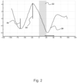
- Fig. 1 depicts a profile 10 of a wafer and a corresponding parabolic fit 12.
- the profile 10 is understood to be exemplary only, as all wafers will have individually determinable profiles that may vary and have differing profiles, and therefore different corresponding parabolic fits.
- the profile 10 represents a profile of a surface of a wafer measured in a cutting direction in which the wafer was cut from an ingot.
- the profile 10 has a very pronounced wavy feature caused by multi-wire sawing, as shown by the oscillating profile 10 in the vertical axis.
- the parabolic fit 12 is a second degree polynomial calculated based on the individual data points that make up the profile 10.
- Fig. 2 depicts a residual 20, which represents data points correlating to the difference between the profile 10 of the exemplary wafer of Fig. 1 and the parabolic fit 12. Specifically, the residual 20 is calculated by subtracting the parabolic fit 12 from the profile 10.
- Coefficient ⁇ of this parabolic equation is the measure of curvature of the peak. Both the amplitude of the peak and its position/height can also be easily determined from this formula:
- Fig. 2 provides an illustration of a sliding window 22 that is exemplary only and captures only a window that has already progressed from the leftmost part of residuals 20 to the center of residuals 20. A parabolic fit is done using data points within this sliding window 22.
- the window should be sufficiently narrow to enable the algorithm to separate individual peaks and valleys and achieve a good quality of fit.
- a variety of window widths may provide adequate results.
- the width of the sliding window 22 is set to 20mm. The criterion for selection of the width of sliding window 22 is based on the ability of an algorithm to separate wafers with a significant waviness from wafers with low waviness.
- the sliding window 22 moves or "slides" one data point at a time along residual 20. For example, if interpolation was done with a step size of 1 mm, the sliding window 22 moves 1 mm at a time.
- Peaks and valleys of the residual may be identified by a software algorithm based on detection of the peaks and valleys in multiple adjacent positions of the sliding window 22 as it moves.
- the software algorithm separates peaks and valleys with amplitude over a predetermined threshold to help eliminate noise.
- the curvatures and amplitudes for each peak are averaged by the software algorithm.
- the respective height 24 of each peak and valley relative to the horizontal axis is determined. Because the horizontal axis corresponds to a wafer having perfect flatness with no variation in height, the respective height 24 of each peak and valley corresponds to wafer shape defects which, if removed, would create a flat wafer.
- the Waviness Parameter formula is used to calculate a total contribution of all peaks and valleys to the Waviness Parameter. For example, the wafer represented by the residual 20 of Fig. 2 would have approximately two peaks and two valleys, resulting in a WavPar that is the sum of four components.
- wafers of varying shape will have variable numbers of peaks and valleys in varying patterns.
- the formulas and methods described above result in a WavPar value that is the sum of identified peaks and valleys representing height variations in the wafer, thus providing advantageous insight into the shape of the wafer over traditional wafer metrics.
- the waviness analysis calculates a linear shape profile from a two-dimensional shape map of the wafer.
- Such embodiments enable exclusion of data points within a certain radius from the center of the wafer (approximately 40 to 45 mm, but up to the radius of the wafer).
- This method may be particularly useful, for example, in 200 mm technology, where older generation metrology tools are equipped with a small diameter chuck to hold the wafer during measurement.
- the wafer is initially chucked in the center, scanned using capacitance probes from the wafer edge to the edge of the chuck. Then the wafer is re-chucked closer to the edge, and the center area is scanned.
- Wafer chucking even on a small chuck, leads to some degree of deformation of a wafer's shape, as the wafer is partly flattened in the chuck area.
- Older generation tool software attempts to stitch wafer maps collected with the two chucking locations. Since wafer shape was distorted by chucking in the two chucking locations, , there is no perfect overlap between these two maps. The process of stitching the maps may create artifacts in the wafer shape, for example because a circular area in the chuck area does not smoothly follow the area outside of the chuck, and can, in rare cases, even lead to false peaks in wafer waviness profiles. Removal of data points from the center of the wafer, from a circle in the middle with radius equal or greater than the chuck size, enables determination of a cleaner linear "shape profile" without such artifacts.
- post-cutting processes may only be implemented for wafers that do not comport within a predetermined threshold of acceptable waviness.
- the degree number of post-processing techniques and/or the degree of post-processing techniques may also be determined based on the determined waviness parameter. In each instance, the waviness parameter determination may thus enhance both quality control processes and the quality of an individual wafer itself.
- the waviness parameter of one wafer can be used to predict the waviness of other wafers, thereby enabling efficient quality control decisions regarding production lots. For example, a determined waviness parameter can be used to predict the waviness of other wafers that would be produced by the same ingot and/or set of multi-wires used in the cutting process. Then, depending on the predicted waviness parameter, the wafers may need to be sorted and or post-processed in different manners depending on the predicted waviness parameter. In this manner, predicted waviness parameters that are within quality control limits can allow for efficient production of wafers without time- and resource-consuming measurements processes for independently determining the waviness of each wafer.
- the waviness parameter enables feedback for performance for multi-wire saws and/or other equipment.
- a baseline waviness parameter may be established by statistical means (e.g. an average or median of historical waviness parameters). Then, the waviness parameter associated with a particular set of multi-wires may be compared to the baseline waviness parameter. Such a comparison would enable quick determination of whether the multi-wires (or other equipment) are operating within acceptable tolerances. Equipment maintenance decisions can then be made based on the comparison of a waviness parameter to the baseline waviness parameter.
- the recitation of "at least one of A, B and C” should be interpreted as one or more of a group of elements consisting of A, B and C, and should not be interpreted as requiring at least one of each of the listed elements A, B and C, regardless of whether A, B and C are related as categories or otherwise.
- the recitation of "A, B and/or C" or "at least one of A, B or C” should be interpreted as including any singular entity from the listed elements, e.g., A, any subset from the listed elements, e.g., A and B, or the entire list of elements A, B and C.
Landscapes
- Engineering & Computer Science (AREA)
- Manufacturing & Machinery (AREA)
- Computer Hardware Design (AREA)
- Microelectronics & Electronic Packaging (AREA)
- Power Engineering (AREA)
- Mechanical Engineering (AREA)
- Mechanical Treatment Of Semiconductor (AREA)
Priority Applications (1)
| Application Number | Priority Date | Filing Date | Title |
|---|---|---|---|
| EP22172684.7A EP4276890A1 (de) | 2022-05-11 | 2022-05-11 | System und verfahren zum bearbeiten von siliziumscheiben |
Applications Claiming Priority (1)
| Application Number | Priority Date | Filing Date | Title |
|---|---|---|---|
| EP22172684.7A EP4276890A1 (de) | 2022-05-11 | 2022-05-11 | System und verfahren zum bearbeiten von siliziumscheiben |
Publications (1)
| Publication Number | Publication Date |
|---|---|
| EP4276890A1 true EP4276890A1 (de) | 2023-11-15 |
Family
ID=82058443
Family Applications (1)
| Application Number | Title | Priority Date | Filing Date |
|---|---|---|---|
| EP22172684.7A Pending EP4276890A1 (de) | 2022-05-11 | 2022-05-11 | System und verfahren zum bearbeiten von siliziumscheiben |
Country Status (1)
| Country | Link |
|---|---|
| EP (1) | EP4276890A1 (de) |
Citations (3)
| Publication number | Priority date | Publication date | Assignee | Title |
|---|---|---|---|---|
| WO2003077309A2 (en) | 2002-03-07 | 2003-09-18 | Memc Electronic Materials, Inc. | Method of predicting post-polishing waviness characteristics of a semiconductor wafer |
| US20120178346A1 (en) * | 2011-01-12 | 2012-07-12 | Siltronic Ag | Method for cooling a workpiece made of semiconductor material during wire sawing |
| WO2021084939A1 (ja) | 2019-10-31 | 2021-05-06 | 信越半導体株式会社 | 半導体ウェーハの評価方法、半導体ウェーハの選別方法及びデバイスの製造方法 |
-
2022
- 2022-05-11 EP EP22172684.7A patent/EP4276890A1/de active Pending
Patent Citations (3)
| Publication number | Priority date | Publication date | Assignee | Title |
|---|---|---|---|---|
| WO2003077309A2 (en) | 2002-03-07 | 2003-09-18 | Memc Electronic Materials, Inc. | Method of predicting post-polishing waviness characteristics of a semiconductor wafer |
| US20120178346A1 (en) * | 2011-01-12 | 2012-07-12 | Siltronic Ag | Method for cooling a workpiece made of semiconductor material during wire sawing |
| WO2021084939A1 (ja) | 2019-10-31 | 2021-05-06 | 信越半導体株式会社 | 半導体ウェーハの評価方法、半導体ウェーハの選別方法及びデバイスの製造方法 |
Non-Patent Citations (4)
| Title |
|---|
| "SEMI M49-0312 Guide for specifying geometry measurement systems for silicon wafers for the 130 nm to 22 nm technology generations", SEMICONDUCTOR EQUIPMENT AND MATERIALS INTERNATIONAL, 2012, Retrieved from the Internet <URL:http://www.semi.org> |
| K.T.TURNERR.RAMKHALAWONJ.K.SINHA: "Role of wafer geometry in wafer chucking", JOURNAL OF MICRO/NANOLITHOGRAPHY, MEMS, AND MOEMS, vol. 12, no. 2, 2013, pages 023007, XP060026359, DOI: 10.1117/1.JMM.12.2.023007 |
| K.TURNER: "Role of process-induced wafer geometry changes in advanced semiconductor manufacturing", SEMICON WEST 2014 CONFERENCE, SAN FRANCISCO, CA, 9 July 2014 (2014-07-09) |
| NUTSCH A. ET AL.: "Determination of Flatness on Patterned Wafer Surfaces Using Wavefront Sensing Methods", PROCEEDINGS OF SPIE, THE INTERNATIONAL SOCIETY FOR OPTICAL ENGINEERING, vol. 7155, 1 October 2008 (2008-10-01), pages 71550Z-1 - 71550Z-1, XP040446124 * |
Similar Documents
| Publication | Publication Date | Title |
|---|---|---|
| JP6312370B2 (ja) | ウェーハジオメトリ計測ツールによるウェーハ表面フィーチャの検出、分類および定量化のためのシステムおよび方法 | |
| CN104428882B (zh) | 半导体晶片的评价方法及制造方法 | |
| JP6265608B2 (ja) | ウェーハ表面計測のための高度化されたサイトベースのナノトポグラフィシステム及び方法 | |
| EP2909857B1 (de) | System, verfahren und metriken zur formcharakterisierung höherer ordnung von wafern und zur wafer-klassifizierung mit geometriewerkzeugen in wafer-grösse | |
| JP4464033B2 (ja) | 半導体ウエーハの形状評価方法及び形状評価装置 | |
| JP4420023B2 (ja) | 半導体ウェーハの測定方法、その製造工程の管理方法、及び半導体ウェーハの製造方法 | |
| WO2021084939A1 (ja) | 半導体ウェーハの評価方法、半導体ウェーハの選別方法及びデバイスの製造方法 | |
| CN111912379A (zh) | 晶圆被加工面加工质量及切割表面切割质量的检验方法 | |
| JP2006294774A (ja) | 半導体ウエーハの評価方法及び評価装置並びに半導体ウエーハの製造方法 | |
| US6613591B1 (en) | Method of estimating post-polishing waviness characteristics of a semiconductor wafer | |
| JP6443520B1 (ja) | 半導体ウェーハの評価方法および該方法を用いた半導体ウェーハの製造方法 | |
| EP4276890A1 (de) | System und verfahren zum bearbeiten von siliziumscheiben | |
| JP3982336B2 (ja) | 半導体ウエーハの加工方法及びプラズマエッチング装置 | |
| US20230339069A1 (en) | System and method for processing silicon wafers | |
| US7810383B2 (en) | Method for evaluating semiconductor wafer, apparatus for evaluating semiconductor wafer, and method for manufacturing semiconductor wafer | |
| KR20220164489A (ko) | 실리콘 웨이퍼의 dic결함의 형상측정방법 및 연마방법 | |
| WO2024057773A1 (ja) | デブリ判定方法 | |
| WO2023106414A1 (ja) | 加工変質層の評価方法及び評価システム | |
| KR100774558B1 (ko) | 나노토포그래피 측정방법 | |
| EP4388579A1 (de) | Systeme und verfahren zur verarbeitung von halbleiterwafern unter verwendung von vorderseitig verarbeiteten wafergeometriemetriken | |
| CN111952208A (zh) | 侦测晶圆设定范围内平整度变化的方法 |
Legal Events
| Date | Code | Title | Description |
|---|---|---|---|
| PUAI | Public reference made under article 153(3) epc to a published international application that has entered the european phase |
Free format text: ORIGINAL CODE: 0009012 |
|
| STAA | Information on the status of an ep patent application or granted ep patent |
Free format text: STATUS: THE APPLICATION HAS BEEN PUBLISHED |
|
| AK | Designated contracting states |
Kind code of ref document: A1 Designated state(s): AL AT BE BG CH CY CZ DE DK EE ES FI FR GB GR HR HU IE IS IT LI LT LU LV MC MK MT NL NO PL PT RO RS SE SI SK SM TR |
|
| STAA | Information on the status of an ep patent application or granted ep patent |
Free format text: STATUS: REQUEST FOR EXAMINATION WAS MADE |
|
| 17P | Request for examination filed |
Effective date: 20240718 |
|
| RBV | Designated contracting states (corrected) |
Designated state(s): AL AT BE BG CH CY CZ DE DK EE ES FI FR GB GR HR HU IE IS IT LI LT LU LV MC MK MT NL NO PL PT RO RS SE SI SK SM TR |