EP4276831A1 - Control circuit and semiconductor memory - Google Patents
Control circuit and semiconductor memory Download PDFInfo
- Publication number
- EP4276831A1 EP4276831A1 EP22789451.6A EP22789451A EP4276831A1 EP 4276831 A1 EP4276831 A1 EP 4276831A1 EP 22789451 A EP22789451 A EP 22789451A EP 4276831 A1 EP4276831 A1 EP 4276831A1
- Authority
- EP
- European Patent Office
- Prior art keywords
- bias
- transistor
- module
- signal
- gate
- Prior art date
- Legal status (The legal status is an assumption and is not a legal conclusion. Google has not performed a legal analysis and makes no representation as to the accuracy of the status listed.)
- Pending
Links
Images



Classifications
-
- H—ELECTRICITY
- H03—ELECTRONIC CIRCUITRY
- H03K—PULSE TECHNIQUE
- H03K19/00—Logic circuits, i.e. having at least two inputs acting on one output; Inverting circuits
- H03K19/20—Logic circuits, i.e. having at least two inputs acting on one output; Inverting circuits characterised by logic function, e.g. AND, OR, NOR, NOT circuits
-
- H—ELECTRICITY
- H03—ELECTRONIC CIRCUITRY
- H03K—PULSE TECHNIQUE
- H03K17/00—Electronic switching or gating, i.e. not by contact-making and –breaking
- H03K17/51—Electronic switching or gating, i.e. not by contact-making and –breaking characterised by the components used
- H03K17/56—Electronic switching or gating, i.e. not by contact-making and –breaking characterised by the components used by the use, as active elements, of semiconductor devices
- H03K17/687—Electronic switching or gating, i.e. not by contact-making and –breaking characterised by the components used by the use, as active elements, of semiconductor devices the devices being field-effect transistors
- H03K17/6871—Electronic switching or gating, i.e. not by contact-making and –breaking characterised by the components used by the use, as active elements, of semiconductor devices the devices being field-effect transistors the output circuit comprising more than one controlled field-effect transistor
-
- G—PHYSICS
- G11—INFORMATION STORAGE
- G11C—STATIC STORES
- G11C11/00—Digital stores characterised by the use of particular electric or magnetic storage elements; Storage elements therefor
- G11C11/21—Digital stores characterised by the use of particular electric or magnetic storage elements; Storage elements therefor using electric elements
- G11C11/34—Digital stores characterised by the use of particular electric or magnetic storage elements; Storage elements therefor using electric elements using semiconductor devices
- G11C11/40—Digital stores characterised by the use of particular electric or magnetic storage elements; Storage elements therefor using electric elements using semiconductor devices using transistors
- G11C11/401—Digital stores characterised by the use of particular electric or magnetic storage elements; Storage elements therefor using electric elements using semiconductor devices using transistors forming cells needing refreshing or charge regeneration, i.e. dynamic cells
- G11C11/4063—Auxiliary circuits, e.g. for addressing, decoding, driving, writing, sensing or timing
- G11C11/407—Auxiliary circuits, e.g. for addressing, decoding, driving, writing, sensing or timing for memory cells of the field-effect type
- G11C11/4074—Power supply or voltage generation circuits, e.g. bias voltage generators, substrate voltage generators, back-up power, power control circuits
-
- G—PHYSICS
- G06—COMPUTING OR CALCULATING; COUNTING
- G06F—ELECTRIC DIGITAL DATA PROCESSING
- G06F1/00—Details not covered by groups G06F3/00 - G06F13/00 and G06F21/00
- G06F1/26—Power supply means, e.g. regulation thereof
- G06F1/32—Means for saving power
- G06F1/3203—Power management, i.e. event-based initiation of a power-saving mode
-
- G—PHYSICS
- G11—INFORMATION STORAGE
- G11C—STATIC STORES
- G11C11/00—Digital stores characterised by the use of particular electric or magnetic storage elements; Storage elements therefor
- G11C11/21—Digital stores characterised by the use of particular electric or magnetic storage elements; Storage elements therefor using electric elements
- G11C11/34—Digital stores characterised by the use of particular electric or magnetic storage elements; Storage elements therefor using electric elements using semiconductor devices
-
- G—PHYSICS
- G11—INFORMATION STORAGE
- G11C—STATIC STORES
- G11C11/00—Digital stores characterised by the use of particular electric or magnetic storage elements; Storage elements therefor
- G11C11/21—Digital stores characterised by the use of particular electric or magnetic storage elements; Storage elements therefor using electric elements
- G11C11/34—Digital stores characterised by the use of particular electric or magnetic storage elements; Storage elements therefor using electric elements using semiconductor devices
- G11C11/40—Digital stores characterised by the use of particular electric or magnetic storage elements; Storage elements therefor using electric elements using semiconductor devices using transistors
- G11C11/401—Digital stores characterised by the use of particular electric or magnetic storage elements; Storage elements therefor using electric elements using semiconductor devices using transistors forming cells needing refreshing or charge regeneration, i.e. dynamic cells
-
- G—PHYSICS
- G11—INFORMATION STORAGE
- G11C—STATIC STORES
- G11C11/00—Digital stores characterised by the use of particular electric or magnetic storage elements; Storage elements therefor
- G11C11/21—Digital stores characterised by the use of particular electric or magnetic storage elements; Storage elements therefor using electric elements
- G11C11/34—Digital stores characterised by the use of particular electric or magnetic storage elements; Storage elements therefor using electric elements using semiconductor devices
- G11C11/40—Digital stores characterised by the use of particular electric or magnetic storage elements; Storage elements therefor using electric elements using semiconductor devices using transistors
- G11C11/401—Digital stores characterised by the use of particular electric or magnetic storage elements; Storage elements therefor using electric elements using semiconductor devices using transistors forming cells needing refreshing or charge regeneration, i.e. dynamic cells
- G11C11/4063—Auxiliary circuits, e.g. for addressing, decoding, driving, writing, sensing or timing
- G11C11/407—Auxiliary circuits, e.g. for addressing, decoding, driving, writing, sensing or timing for memory cells of the field-effect type
- G11C11/4072—Circuits for initialization, powering up or down, clearing memory or presetting
-
- G—PHYSICS
- G11—INFORMATION STORAGE
- G11C—STATIC STORES
- G11C11/00—Digital stores characterised by the use of particular electric or magnetic storage elements; Storage elements therefor
- G11C11/21—Digital stores characterised by the use of particular electric or magnetic storage elements; Storage elements therefor using electric elements
- G11C11/34—Digital stores characterised by the use of particular electric or magnetic storage elements; Storage elements therefor using electric elements using semiconductor devices
- G11C11/40—Digital stores characterised by the use of particular electric or magnetic storage elements; Storage elements therefor using electric elements using semiconductor devices using transistors
- G11C11/401—Digital stores characterised by the use of particular electric or magnetic storage elements; Storage elements therefor using electric elements using semiconductor devices using transistors forming cells needing refreshing or charge regeneration, i.e. dynamic cells
- G11C11/4063—Auxiliary circuits, e.g. for addressing, decoding, driving, writing, sensing or timing
- G11C11/407—Auxiliary circuits, e.g. for addressing, decoding, driving, writing, sensing or timing for memory cells of the field-effect type
- G11C11/4076—Timing circuits
-
- G—PHYSICS
- G11—INFORMATION STORAGE
- G11C—STATIC STORES
- G11C11/00—Digital stores characterised by the use of particular electric or magnetic storage elements; Storage elements therefor
- G11C11/21—Digital stores characterised by the use of particular electric or magnetic storage elements; Storage elements therefor using electric elements
- G11C11/34—Digital stores characterised by the use of particular electric or magnetic storage elements; Storage elements therefor using electric elements using semiconductor devices
- G11C11/40—Digital stores characterised by the use of particular electric or magnetic storage elements; Storage elements therefor using electric elements using semiconductor devices using transistors
- G11C11/401—Digital stores characterised by the use of particular electric or magnetic storage elements; Storage elements therefor using electric elements using semiconductor devices using transistors forming cells needing refreshing or charge regeneration, i.e. dynamic cells
- G11C11/4063—Auxiliary circuits, e.g. for addressing, decoding, driving, writing, sensing or timing
- G11C11/407—Auxiliary circuits, e.g. for addressing, decoding, driving, writing, sensing or timing for memory cells of the field-effect type
- G11C11/408—Address circuits
- G11C11/4082—Address Buffers; level conversion circuits
-
- G—PHYSICS
- G11—INFORMATION STORAGE
- G11C—STATIC STORES
- G11C11/00—Digital stores characterised by the use of particular electric or magnetic storage elements; Storage elements therefor
- G11C11/21—Digital stores characterised by the use of particular electric or magnetic storage elements; Storage elements therefor using electric elements
- G11C11/34—Digital stores characterised by the use of particular electric or magnetic storage elements; Storage elements therefor using electric elements using semiconductor devices
- G11C11/40—Digital stores characterised by the use of particular electric or magnetic storage elements; Storage elements therefor using electric elements using semiconductor devices using transistors
- G11C11/401—Digital stores characterised by the use of particular electric or magnetic storage elements; Storage elements therefor using electric elements using semiconductor devices using transistors forming cells needing refreshing or charge regeneration, i.e. dynamic cells
- G11C11/4063—Auxiliary circuits, e.g. for addressing, decoding, driving, writing, sensing or timing
- G11C11/407—Auxiliary circuits, e.g. for addressing, decoding, driving, writing, sensing or timing for memory cells of the field-effect type
- G11C11/409—Read-write [R-W] circuits
- G11C11/4093—Input/output [I/O] data interface arrangements, e.g. data buffers
-
- G—PHYSICS
- G11—INFORMATION STORAGE
- G11C—STATIC STORES
- G11C5/00—Details of stores covered by group G11C11/00
- G11C5/14—Power supply arrangements, e.g. power down, chip selection or deselection, layout of wirings or power grids, or multiple supply levels
- G11C5/148—Details of power up or power down circuits, standby circuits or recovery circuits
-
- G—PHYSICS
- G11—INFORMATION STORAGE
- G11C—STATIC STORES
- G11C7/00—Arrangements for writing information into, or reading information out from, a digital store
- G11C7/10—Input/output [I/O] data interface arrangements, e.g. I/O data control circuits, I/O data buffers
- G11C7/1078—Data input circuits, e.g. write amplifiers, data input buffers, data input registers, data input level conversion circuits
- G11C7/109—Control signal input circuits
-
- G—PHYSICS
- G11—INFORMATION STORAGE
- G11C—STATIC STORES
- G11C7/00—Arrangements for writing information into, or reading information out from, a digital store
- G11C7/22—Read-write [R-W] timing or clocking circuits; Read-write [R-W] control signal generators or management
- G11C7/222—Clock generating, synchronizing or distributing circuits within memory device
-
- G—PHYSICS
- G11—INFORMATION STORAGE
- G11C—STATIC STORES
- G11C7/00—Arrangements for writing information into, or reading information out from, a digital store
- G11C7/22—Read-write [R-W] timing or clocking circuits; Read-write [R-W] control signal generators or management
- G11C7/225—Clock input buffers
-
- G—PHYSICS
- G11—INFORMATION STORAGE
- G11C—STATIC STORES
- G11C8/00—Arrangements for selecting an address in a digital store
- G11C8/06—Address interface arrangements, e.g. address buffers
-
- G—PHYSICS
- G11—INFORMATION STORAGE
- G11C—STATIC STORES
- G11C2207/00—Indexing scheme relating to arrangements for writing information into, or reading information out from, a digital store
- G11C2207/22—Control and timing of internal memory operations
- G11C2207/2227—Standby or low power modes
-
- Y—GENERAL TAGGING OF NEW TECHNOLOGICAL DEVELOPMENTS; GENERAL TAGGING OF CROSS-SECTIONAL TECHNOLOGIES SPANNING OVER SEVERAL SECTIONS OF THE IPC; TECHNICAL SUBJECTS COVERED BY FORMER USPC CROSS-REFERENCE ART COLLECTIONS [XRACs] AND DIGESTS
- Y02—TECHNOLOGIES OR APPLICATIONS FOR MITIGATION OR ADAPTATION AGAINST CLIMATE CHANGE
- Y02D—CLIMATE CHANGE MITIGATION TECHNOLOGIES IN INFORMATION AND COMMUNICATION TECHNOLOGIES [ICT], I.E. INFORMATION AND COMMUNICATION TECHNOLOGIES AIMING AT THE REDUCTION OF THEIR OWN ENERGY USE
- Y02D10/00—Energy efficient computing, e.g. low power processors, power management or thermal management
Definitions
- the disclosure relates to the technical field of semiconductors, in particular to a control circuit and a semiconductor memory.
- DDR Double Data Rate
- DRAM Dynamic Random Access Memory
- the disclosure provides a control circuit and a semiconductor memory, which can not only ensure the settle time of a bias module, but also achieve the purpose of saving power.
- the control circuit includes a bias module.
- the bias module is configured to provide a bias current for a functional module.
- the bias module includes a first bias module and a second bias module.
- the first bias module is configured to provide a first bias current
- the second bias module is configured to provide a second bias current.
- the first bias current is smaller than the second bias current
- the first bias module is configured to be in a normally open state after being powered on
- the second bias module is configured to receive a bias enabling signal and provide the second bias current based on the bias enabling signal.
- a functional module is configured to receive an excitation signal and to be started based on the excitation signal.
- a time point when the functional module receives the excitation signal is later than a time point when the bias module receives the bias enabling signal.
- control circuit further includes an enabling module.
- the enabling module is configured to receive a power switching signal and output a bias enabling signal and an excitation signal based on the power switching signal.
- the power switching signal characterizes starting the functional module.
- the power switching signal includes a preceding first changing edge and a subsequent second changing edge.
- the enabling module is further configured to output the bias enabling signal at the first changing edge, and configured to output the excitation signal at the second changing edge.
- a changing direction of the first changing edge is opposite to a changing direction of the second changing edge.
- the first changing edge is switched from a low level state to a high level state
- the second changing edge is switched from a high level state to a low level state
- the enabling module is further configured to receive a state signal, perform logical operation processing based on the power switching signal and the state signal, and output a bias enabling signal and an excitation signal.
- the state signal characterizes that the control circuit is in a Power Down State or a Power On State.
- the enabling module includes a first logic module and a second logic module.
- the first logic module is configured to receive a power switching signal and a state signal, and perform first logic operation on the power switching signal and the state signal to output a bias enabling signal.
- the second logic module is configured to receive the power switching signal and the state signal, and perform second logic operation on the power switching signal and the state signal to output an excitation signal.
- the first logic module includes a first NOR gate, a second NOR gate and a first NOT gate.
- one input end of the first NOR gate is configured to receive a power switching signal, and the other input end of the first NOR gate is connected with an output end of the second NOR gate.
- One input end of the second NOR gate is connected with an output end of the first NOR gate, and the other input end of the second NOR gate is configured to receive a state signal, and the output end of the second NOR gate is also connected with an input end of the first NOT gate.
- the second logic module includes a second NOT gate, a first NAND gate, a second NAND gate and a third NOT gate.
- an input end of the second NOT gate is configured to receive a state signal.
- An output end of the second NOT gate is connected with one input end of the first NAND gate, the other input end of the first NAND gate is connected with an output end of the second NAND gate, an output end of the first NAND gate is connected with one input end of the second NAND gate, the other input end of the second NAND gate is configured to receive a power switching signal, and the output end of the first NAND gate is also connected with an input end of the third NOT gate.
- the functional module includes an input buffer circuit.
- the first bias module is connected in parallel with the second bias module. Moreover, the first bias module includes a first bias resistor, and the second bias module includes a second bias resistor. Herein, a resistance value of the first bias resistor is greater than a resistance value of the second bias resistor.
- the first bias module further includes a first transistor, a second transistor, a third transistor and a fourth transistor.
- a drain electrode of the first transistor and a drain electrode of the second transistor are both connected with a power supply terminal
- a gate electrode of the first transistor and a gate electrode of the second transistor are both connected with a ground terminal
- a source electrode of the first transistor is connected with a drain electrode of the third transistor
- a source electrode of the second transistor is connected with a drain electrode of the fourth transistor
- a gate electrode of the third transistor and a gate electrode of the fourth transistor are both connected with a source electrode of the third transistor
- the source electrode of the third transistor is connected with a ground terminal through the first bias resistor.
- a source electrode of the fourth transistor is connected with a functional module, and configured to provide a first bias current for the functional module.
- the second bias module further includes a fifth transistor, a sixth transistor, a seventh transistor and an eighth transistor.
- a drain electrode of the fifth transistor and a drain electrode of the sixth transistor are both connected with a power supply terminal
- a gate electrode of the fifth transistor and a gate electrode of the sixth transistor are both connected with a bias enabling signal
- a source electrode of the fifth transistor is connected with a drain electrode of the seventh transistor
- a source electrode of the sixth transistor is connected with a drain electrode of the eighth transistor
- a gate electrode of the seventh transistor and a gate electrode of the eighth transistor are both connected with a source electrode of the seventh transistor
- the source electrode of the seventh transistor is connected with a ground terminal through the second bias resistor.
- a source electrode of the eighth transistor is connected with a functional module, and configured to provide a second bias current for the functional module.
- a semiconductor memory which may include a control circuit as in the first aspect.
- the embodiments of the present disclosure provide a control circuit and a semiconductor memory.
- the control circuit includes a bias module.
- the bias module is configured to provide a bias current for a functional module.
- the bias module includes a first bias module and a second bias module.
- the first bias module is configured to provide a first bias current
- the second bias module is configured to provide a second bias current.
- the first bias current is smaller than the second bias current
- the first bias module is configured to be in a normally open state after being powered on
- the second bias module is configured to receive a bias enabling signal and provide the second bias current based on the bias enabling signal.
- the first bias module and the second bias module are arranged, and the first bias module which provides a smaller bias current is in a normally open state, so that the control circuit can not only ensure the settle time of the bias module, avoid the problem that the tXP time is occupied due to long recovery time of the bias module, but also achieve the purpose of saving power.
- first/second/third involved in the embodiments of the disclosure are only for distinguishing similar objects and do not represent a specific sequence of the objects. It can be understood that “first/second/third” may be interchanged to specific sequences or orders if allowed to implement the embodiments of the disclosure described herein in sequences except the illustrated or described ones.
- the high level and low level used by a signal related to the embodiments of the present disclosure refer to logic level of the signal.
- a signal with a high level is different from same with a low level.
- the high level may correspond to a signal with a first voltage
- the low level may correspond to a signal with a second voltage.
- the first voltage is greater than the second voltage.
- the logic level of the signal may be different from or opposite to the described logic level.
- a signal described as having a logic "high” level may alternatively have a logic "low” level
- a signal described as having a logic "low” level may alternatively have a logic "high” level.
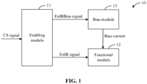
- FIG. 1 is a schematic diagram of a composition structure of a control circuit.
- the control circuit 10 may include an enabling module 11, a functional module 12 and a bias module 13.
- the enabling module 11 is configured to receive a power switching signal and output a bias enabling signal and an excitation signal according to the power switching signal.
- the functional module 12 is connected with the enabling module 11 and configured to receive the excitation signal to start the functional module 12.
- the bias module 13 is connected with the enabling module 11 and configured to receive a bias enabling signal to start the bias module 13.
- the bias module 13 is also connected with the functional module 12 and configured to provide a bias current for the functional module 12.
- the power switching signal may be represented by CS
- the bias enabling signal may be represented by EnIBBias
- the excitation signal may be represented by EnIB.
- the CS signal is configured to characterize that the control circuit 10 is switched from a Power Down State to a Power On State, so as to start the functional module 12 and the bias module 13.
- the EnIB signal is an enabling signal provided for the functional module 12 to start the functional module 12
- the EnIBBias signal is an enabling signal provided for the bias module 13 to start the bias module 13.
- FIG. 2 is a schematic diagram of a signal timing sequence of a control circuit 10.
- the control circuit 10 may include a Power Down State and a Power on State.
- the CS signal is a pulse signal with a valid high-level.
- the control circuit 10 At a first changing edge of the CS signal (that is, when switching from a low-level state to a high-level state), the control circuit 10 is in a Power Down State, but starts to switch the state.
- a second changing edge of the CS signal that is, when switching from a high-level state to a low-level state
- the control circuit 10 enters a Power On State.
- the EnIB signal and the EnIBBias signal are also in an enabling state (that is, switching from a low-level state to a high-level state), which means that the functional module 12 and the bias module 13 are started.
- the functional module 12 and the bias module 13 are powered down.
- the Recovery time of the bias module 13 is longer, which not only takes up the tXP time, but also may cause waste of power consumption due to longer Recovery time.
- the tXP time represents the time of Exit Power Down to Next One Command Delay.
- the embodiments of the disclosure provide a control circuit.
- the first bias module and the second bias module are arranged, and the first bias module which provides a smaller bias current is in a normally open state, so that the control circuit can not only ensure the settle time of the bias module, avoid the problem that the tXP time is occupied due to long recovery time of the bias module, but also achieve the purpose of saving power.
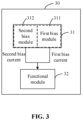
- FIG. 3 is a schematic diagram of a composition structure of a control circuit according to an embodiment of the present disclosure.
- the control circuit 30 may include a bias module 31, and the bias module 31 is configured to provide a bias current for the functional module 32.
- the bias module 31 includes a first bias module 311 and a second bias module 312.
- the first bias module 311 is configured to provide a first bias current
- the second bias module 312 is configured to provide a second bias current.
- the first bias current is smaller than the second bias current
- the first bias module 311 is configured to be in a normally open state after being powered on
- the second bias module 312 is configured to receive a bias enabling signal and provide the second bias current based on the bias enabling signal.
- control circuit 30 may be applied to multiple circuit scenarios, especially to a power-saving control circuit scenario of a DDR5 memory with Low Power (LP), but it does not constitute a relevant limitation.
- LP Low Power
- the first bias module 311 and the second bias module 312 are connected in parallel.
- the first bias module 311 may also be called a low power bias module.
- the bias module is in a normally open state. That is, the first bias module 311 will not be powered down in the case where the associated functional module does not work, or as long as a device (for example, a memory) contains the circuit, the device is in a Power On State.
- the second bias module 312 may also be called a Normal bias module, and the bias module will be powered down when the associated functional module is in a Power Down State and does not work.
- the Recovery time of the whole bias module may be reduced to save the settle time of the bias module.
- the settle time refers to the time required for the bias module to reach a target settle state.
- the functional module 32 is configured to receive an excitation signal and to be started based on the excitation signal.
- the time point when the functional module 32 receives the excitation signal is later than the time point when the bias module receives the corresponding bias enabling signal.
- the functional module 12 may be an input buffer circuit, such as a Command Address (CA) / Clock (Clk) input buffer circuit.
- CA Command Address
- Clk Clock
- the excitation signal may be represented by EnIB
- the bias enabling signal may be represented by EnIBBias.
- the bias enabling signal is configured to start the bias module 31 (specifically the second bias module 312)
- the excitation signal is configured to start the functional module 32.
- the bias module 31 can be enabled to start only after a certain recovery time, and only when the enable starting of the bias module is consistent with the enable starting of the functional module, the power loss will not be caused. That is, it is best that the time point when the bias module 31 is recovered is consistent with the time point when the functional module is enabled to start. Therefore, in order not to waste power, the time point when the functional module receives the excitation signal needs to be later than the time point when the bias module receives the corresponding bias enabling signal, so as to reserve a certain recovery time for the bias module.
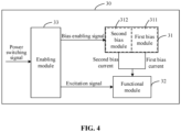
- control circuit 30 may also include an enabling module 33.
- the enabling module 33 is configured to receive a power switching signal and output a bias enabling signal and an excitation signal based on the power switching signal.
- the power switching signal characterizes starting the functional module.
- the power switching signal may be represented by CS, and the CS signal is a pulse signal.
- the pulse width is at least 3 nanoseconds.
- the CS signal is also configured to characterize that the control circuit 10 is switched from the Power Down State to the Power On State, so that the control circuit 10 can start the functional module 32 after being powered on.
- the power switching signal is a pulse signal
- the power switching signal may include a preceding first changing edge and a subsequent second changing edge.
- the enabling module 33 is further configured to output the bias enabling signal at the first changing edge, and configured to output the excitation signal at the second changing edge.
- the time point when the bias enabling signal enters an enabling state needs to be earlier than the time point when the excitation signal enters the enabling state, so that the recovery time may be reserved for the bias module before the excitation signal is enabled.
- the enabling module 33 may output the bias enabling signal at the first changing edge and output the excitation signal at the second changing edge, so that the settle time of the bias module is increased by the pulse time of the CS signal, and the tXP time may be avoided from being occupied.
- the changing direction of the first changing edge is opposite to the changing direction of the second changing edge.
- the first changing edge and the second changing edge may be a rising edge and a falling edge, which are of different pulse signals transmitted successively.
- the first changing edge may be switched from a low level state to a high level state
- the second changing edge may be switched from a high level state to a low level state
- the first changing edge may be switched from a high-level state to a low-level state, and the second changing edge may be switched from a low-level state to a high-level state.
- the CS signal is a valid high-level pulse signal
- the first changing edge may be switched from a low-level state to a high-level state
- the second changing edge may be switched from a high-level state to a low-level state, which is not limited in the embodiment of the present disclosure.
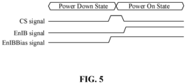
- FIG. 5 is a schematic diagram of a signal timing sequence according to an embodiment of the present disclosure.
- the control circuit 30 may also include a Power Down State and a Power On State. Then, the EnIBBias signal is output at the first changing edge of the CS signal, and the EnIB signal is output at the second changing edge of the CS signal, so that the time point when EnIBBias is in the enabling state is earlier than the time point when the EnIB signal is in the enabling state.
- the first changing edge of the CS signal is in the period with the Power Down State
- the second changing edge of the CS signal is in the period with the Power On State.
- the second bias module 312 may be started at a switching point between the Power Down State and the Power On State since there is a signal delay, so that the final starting of the second bias module 312 is in the period with the Power On State. Since the functional module receives the enabling signal and enters the enabling state when being in the Power On State, the time point when the EnIB signal is provided for the functional module 32 is later than the time point when the EnIBBias signal is provided for the second bias module 312. That is, the recovery time is reserved for the bias module (specifically, the second bias module), which facilitates preventing the functional module 32 from incapability of working normally in the case of ensuring the settle time of the bias module, thus saving power.
- the enabling module 33 is further configured to receive a state signal, perform logical operation processing based on the power switching signal and the state signal, and output a bias enabling signal and an excitation signal.
- the state signal characterizes that the control circuit is in a Power Down State or a Power On State.
- the state signal may be represented by PowerDn.
- PowerDn when the PowerDn signal is in a high level state, it characterizes that the control circuit 30 is in the Power Down State.
- PowerDn signal when the PowerDn signal is in a low level state, it characterizes that the control circuit 30 is in the Power On State.
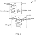
- the enabling module 33 may include a first logic module 331 and a second logic module 332.
- the first logic module 331 is configured to receive a power switching signal and a state signal, and perform first logic operation on the power switching signal and the state signal to output a bias enabling signal.
- the second logic module 332 is configured to receive a power switching signal and a state signal, and perform second logic operation on the power switching signal and the state signal to output an excitation signal.
- the input of the first logic module 331 is the CS signal and PowerDn signal, and the output is the EnIBBias signal.
- the input of the second logic module 332 is the CS signal and PowerDn signal, and the output is the EnIB signal.
- the first logic module 331 may include a first NOR gate a, a second NOR gate b and a first NOT gate c.
- One input end of the first NOR gate a is configured to receive a power switching signal, and the other input end of the first NOR gate a is connected with an output end of the second NOR gate b.
- One input end of the second NOR gate b is connected with an output end of the first NOR gate a, and the other input end of the second NOR gate b is configured to receive a state signal, and the output end of the second NOR gate b is also connected with the input end of the first NOT gate c.
- an output end of the first NOT gate c is configured to output a bias enabling signal.
- the bias enabling signal output by the first logic module 331 is in the second level state.
- the bias enabling signal output by the first logic module 331 is in the second level state.
- the first level state is a low level state
- the second level state is a high level state.
- the EnIBBias signal at the time is switched from the low level state to the high level state.
- the EnIBBias signal at the time remains in the high level state.
- the EnIBBias signal is in the high level state, which means that the EnIBBias signal is in an enabling state. That is, at the rising edge moment of the CS signal (that is, switched from the low level state to the high-level state), the EnIBBias signal is in the enabling state.
- the second logic module 332 may include a second NOT gate d, a first NAND gate e, a second NAND gate f and a third NOT gate g.
- An input end of the second NOT gate d is configured to receive a state signal.
- An output end of the second NOT gate d is connected with one input end of the first NAND gate e, the other input end of the first NAND gate e is connected with an output end of the second NAND gate f, an output end of the first NAND gate e is connected with one input end of the second NAND gate f, the other input end of the second NAND gate f is configured to receive a power switching signal, and the output end of the first NAND gate e is also connected with an input end of the third NOT gate g.
- an output end of the first NOT gate g is configured to output an excitation signal.
- the excitation signal output by the second logic module 332 is in the first level state.
- the excitation signal output by the second logic module 332 is in the second level state.
- the first level state is a low level state
- the second level state is a high level state.
- the EnIB signal at the time remains in the low level state.
- the EnIB signal at the time is switched from the low level state to the high level state.
- the EnIB signal is in the high level state, which means that the EnIB signal is in an enabling state.
- the EnIB signal is in the enabling state. That is, the EnIB signal is in the enabling state later than the EnIBBias signal is in the enabling state.
- FIG. 7 is a schematic diagram of a detailed structure of a control circuit 30 according to an embodiment of the present disclosure.
- the first bias module 311 is connected in parallel with the second bias module 312.
- the first bias module 311 may include a first bias resistor MR1
- the second bias module 312 may include a second bias resistor MR2.
- a resistance value of the first bias resistor MR1 is greater than a resistance value of the second bias resistor MR2.
- the first bias resistor MR1 may contain a plurality of sub-bias resistors
- the second bias resistor MR2 may also contain a plurality of sub-bias resistors. That is, the equivalent resistance value of the plurality of sub-bias resistors in the first bias resistor MR1 needs to be greater than the equivalent resistance value of the plurality of sub-bias resistors in the second bias resistor MR2.
- the number of the sub-bias resistors included in the first bias resistor MR1 is greater than the number of the sub-bias resistors included in the second bias resistor MR2.
- the first bias module 311 may include four transistors in addition to the first bias resistor. In some embodiments, as illustrated in FIG. 7 , the first bias module 311 may further include a first transistor MP1, a second transistor MP2, a third transistor MP3 and a fourth transistor MP4.
- a drain electrode of the first transistor MP1 and a drain electrode of the second transistor MP2 are both connected with a power supply terminal.
- a gate electrode of the first transistor MP1 and a gate electrode of the second transistor MP2 are both connected with a ground terminal.
- a source electrode of the first transistor MP1 is connected with a drain electrode of the third transistor MP3, and a source electrode of the second transistor MP2 is connected with a drain electrode of the fourth transistor MP4.
- a gate electrode of the third transistor MP3 and a gate electrode of the fourth transistor MP4 are both connected with a source electrode of the third transistor MP3, and the source electrode of the third transistor MP3 is connected with the ground terminal through the first bias resistor MR1.
- a source electrode of the fourth transistor MP4 is connected with a functional module 32, and is configured to provide a first bias current for the functional module 32.
- the second bias module 312 may also include four transistors in addition to the second bias resistor. In some embodiments, as illustrated in FIG. 7 , in some embodiments, the second bias module 312 may further include a fifth transistor MP5, a sixth transistor MP6, a seventh transistor MP7 and an eighth transistor MP8.
- a drain electrode of the fifth transistor MP5 and a drain electrode of the sixth transistor MP6 are both connected with a power supply terminal.
- a gate electrode of the fifth transistor MP5 and a gate electrode of the sixth transistor MP6 are both connected with a bias enabling signal.
- a source electrode of the fifth transistor MP5 is connected with a drain electrode of the seventh transistor MP7, and a source electrode of the sixth transistor MP6 is connected with a drain electrode of the eighth transistor MP8.
- a gate electrode of the seventh transistor MP7 and a gate electrode of the eighth transistor MP8 are both connected with a source electrode of the seventh transistor MP7, and the source electrode of the seventh transistor MP7 is connected with a ground terminal through the second bias resistor MR2.
- a source electrode of the eighth transistor MP8 is connected with a functional module 32, and is configured to provide a second bias current for the functional module 32.
- the first transistor MP1, the second transistor MP2, the third transistor MP3, the fourth transistor MP4, the fifth transistor MP5, the sixth transistor MP6, the seventh transistor MP7, and the eighth transistor MP8 are all PMOS transistors.
- the power supply terminal is represented by VCC
- the ground terminal is represented by VSS.
- the input signals of the gate electrode of the first transistor MP1 and the gate electrode of the second transistor MP2 are VSS signals, so that the two transistors are in a normally open state
- the input signals of the gate electrode of the third transistor MP3 and the gate electrode of the fourth transistor MP4 are represented by BiasN
- the BiasN signal is generated by connecting the first bias resistor MR1 to the ground terminal, and is configured to control the conduction states of the third transistor MP3 and the fourth transistor MP4, so as to provide the first bias current for the functional module 32.
- the input signals of the gate electrode of the fifth transistor MP5 and the gate electrode of the sixth transistor MP6 are EnIBBias signals, so as to control the conduction states of the fifth transistor MP5 and the sixth transistor MP6 according to the EnIBBias signals, while the input signals of the gate electrode of the seventh transistor MP7 and the gate electrode of the eighth transistor MP8 are generated by connecting the second bias resistor MR2 to the ground terminal, and are configured to control the conduction states of the seventh transistor MP7 and the eighth transistor MP8, so as to provide the second bias current for the functional module 32.
- the second bias module 311 may also include a ninth transistor MP9.
- the drain electrode of the ninth transistor MP9 is connected with the power supply terminal
- the gate electrode of the ninth transistor MP9 is connected with the bias enabling signal
- the source electrode of the ninth transistor MP9 is connected with the functional module 32 and configured to supply power supply voltage to the functional module 32.
- the functional module 32 may include an input buffer circuit.
- the input buffer circuit when the control circuit 30 is in the Power On State, the input buffer circuit may be provided with a first bias current through the first bias module 311, the input buffer circuit may be provided with a second bias current through the second bias module 312, and the first bias current is smaller than the second bias current.
- the embodiment provides a control circuit.
- the control circuit includes a bias module.
- the bias module is configured to provide a bias current for a functional module.
- the bias module includes a first bias module and a second bias module.
- the first bias module is configured to provide a first bias current
- the second bias module is configured to provide a second bias current.
- the first bias current is smaller than the second bias current
- the first bias module is configured to be in a normally open state after being powered on
- the second bias module is configured to receive a bias enabling signal and provide the second bias current based on the bias enabling signal.
- the first bias module and the second bias module are arranged, and the first bias module which provides a smaller bias current is in a normally open state, so that the control circuit can not only ensure the settle time of the bias module, avoid the problem that the tXP time is occupied due to long recovery time of the bias module, but also achieve the purpose of saving power.
- FIG. 8 is a schematic diagram of a detailed structure of another control circuit 30 according to an embodiment of the present disclosure.
- the control circuit 30 may include a first resistor R1, a second resistor R2, a third resistor R3, a fourth resistor R4, a fifth resistor R5, a sixth resistor R6, a first transistor MP1, a second transistor MP2, a third transistor MP3, a fourth transistor MP4, a fifth transistor MP5, a sixth transistor MP6, a seventh transistor MP7, an eighth transistor MP8, a ninth transistor MP9, a tenth transistor MP10, an eleventh transistor MN1, a twelfth transistor MN2, a thirteenth transistor MP11, a fourteenth transistor MP 12, a fifteenth transistor MN3 and a sixteenth transistor MN4.
- the first transistor MP1, the second transistor MP2, the third transistor MP3, the fourth transistor MP4, the fifth transistor MP5, the sixth transistor MP6, the seventh transistor MP7, the eighth transistor MP8, the ninth transistor MP9, the tenth transistor MP10, the thirteenth transistor MP11, and the fourteenth transistor MP12 are PMOS transistors
- the eleventh transistor MN1, the twelfth transistor MN2, the fifteenth transistor MN3 and the sixteenth transistor MN4 are NMOS transistors.
- the first resistor R1, the second resistor R2, the third resistor R3, the fourth resistor R4 and the fifth resistor R5 with the first transistor MP1, the second transistor MP2, the third transistor MP3, and the fourth transistor MP4 form a first bias module
- the sixth resistor R6 with the fifth transistor MP5, the sixth transistor MP6, the seventh transistor MP7, and the eighth transistor MP8 forms a second bias module.
- the first resistor R1, the second resistor R2, the third resistor R3, the fourth resistor R4 and the fifth resistor R5 are connected in series to form a first bias resistor.
- the sixth resistor R6 forms a second bias resistor.
- the functional module takes the input buffer circuit as an example.
- the tenth transistor MP10, the eleventh transistor MN1, the twelfth transistor MN2, the thirteenth transistor MP11, the fourteenth transistor MP12, the fifteenth transistor MN3, and the sixteenth transistor MN4 constitute the input buffer circuit.
- the drain electrode of the thirteenth transistor MP11 is connected with the source electrode of the fourth transistor MP4 for receiving the first bias current.
- the drain electrode of the fourteenth transistor MP12 is connected with the source electrode of the eighth transistor MP8 for receiving the second bias current.
- the gate electrode of the thirteenth transistor MP11 is configured to receive a Command Address signal (represented by CA).
- the gate electrode of the fourteenth transistor MP12 is configured to receive a reference signal (represented by Vref).
- the source electrode of the thirteenth transistor MP11 is connected with the drain electrode of the fifteenth transistor MN3, and also connected with the gate electrode of the fifteenth transistor MN3 and the gate electrode of the sixteenth transistor MN4.
- the source electrode of the fourteenth transistor MP12 is connected with the drain electrode of the sixteenth transistor MN4 for outputting a Stage Output signal (represented by StgOut).
- the source electrode of the fifteenth transistor MN3 and the source electrode of the sixteenth transistor MN4 are both connected with the ground terminal.
- the drain electrode of the tenth transistor MP10 is connected with the source electrode of the ninth transistor MP9 for receiving power supply voltage.
- the gate electrode of the tenth transistor MP10 and the gate electrode of the eleventh transistor MN1 are both connected with the source electrode of the fourteenth transistor MP12, for receiving the StgOut signal.
- the source electrode of the tenth transistor MP10 is connected with the drain electrode of the eleventh transistor MN1 for outputting a Command Address Output signal (represented by CAOUT).
- the source electrode of the eleventh transistor MN1 is connected with the drain electrode of the twelfth transistor MN2, the gate electrode of the twelfth transistor MN2 is configured to receive an excitation signal (represented by EnIB), and the source electrode of the twelfth transistor MN2 is connected with the ground terminal.
- the embodiment of the disclosure provides a control circuit.
- the specific implementation of the previous embodiment is described in detail. It is to be seen that the first bias module and the second bias module are arranged, and the first bias module that provides a smaller bias current is in a normally open state. Meanwhile, based on the timing sequence control of the enabling signals of the input buffer circuit and the bias module, the control circuit can not only ensure the settle time of the bias module, but also achieve the purpose of saving power.
- FIG. 9 is a schematic diagram of a composition structure of a semiconductor memory 90 according to an embodiment of the present disclosure.
- the semiconductor memory 90 may include the control circuit 30 of any of the previous embodiments.
- the semiconductor memory 90 is a DRAM chip.
- the DRAM chip conforms to the DDR5 memory specification.
- the embodiment of the present disclosure relates to semiconductor integrated circuit design, in particular to an analog circuit. Specifically, a power-saving control circuit design that can implement LP DDR5 is mainly provided here.
- the first bias module and the second bias module are arranged in the control circuit, and the first bias module that provides a smaller bias current is in a normally open state. Meanwhile, based on timing sequence control of enabling signals of the input buffer circuit and the bias module, the control circuit can not only ensure the settle time of the bias module, avoid the problem that the tXP time is occupied due to long recovery time of the bias module, but also achieve the purpose of saving power.
- sequence numbers of the embodiments of the disclosure are adopted not to represent superiority-inferiority of the embodiments but only for description.
- the embodiments of the present disclosure provide a control circuit and a semiconductor memory.
- the control circuit includes a bias module.
- the bias module is configured to provide a bias current for a functional module.
- the bias module includes a first bias module and a second bias module.
- the first bias module is configured to provide a first bias current
- the second bias module is configured to provide a second bias current.
- the first bias current is smaller than the second bias current
- the first bias module is configured to be in a normally open state after being powered on
- the second bias module is configured to receive a bias enabling signal and provide the second bias current based on the bias enabling signal.
- the first bias module and the second bias module are arranged, and the first bias module which provides a smaller bias current is in a normally open state, so that the control circuit can not only ensure the settle time of the bias module, avoid the problem that the tXP time is occupied due to long recovery time of the bias module, but also achieve the purpose of saving power.
Landscapes
- Engineering & Computer Science (AREA)
- Computer Hardware Design (AREA)
- Microelectronics & Electronic Packaging (AREA)
- Physics & Mathematics (AREA)
- General Engineering & Computer Science (AREA)
- Computing Systems (AREA)
- Mathematical Physics (AREA)
- Theoretical Computer Science (AREA)
- Power Engineering (AREA)
- General Physics & Mathematics (AREA)
- Logic Circuits (AREA)
- Dram (AREA)
- Power Sources (AREA)
Abstract
Description
- The application is filed based upon and claims priority to
Chinese patent application No. 202210306176.4, filed on March 25, 2022 - The disclosure relates to the technical field of semiconductors, in particular to a control circuit and a semiconductor memory.
- With the continuous development of semiconductor technology, the speed of data transmission is increasingly demanded when devices such as computers are manufactured and used. In order to achieve a faster data transmission speed, a series of devices such as memory in which data can be transmitted at Double Data Rate (DDR) have been developed.
- In Dynamic Random Access Memory (DRAM), in order to save power, both an input buffer module and a bias module need to be powered down when the memory enters a Power Down State.
- The disclosure provides a control circuit and a semiconductor memory, which can not only ensure the settle time of a bias module, but also achieve the purpose of saving power.
- According to a first aspect of the present disclosure, there is provided a control circuit. The control circuit includes a bias module. The bias module is configured to provide a bias current for a functional module. The bias module includes a first bias module and a second bias module. The first bias module is configured to provide a first bias current, and the second bias module is configured to provide a second bias current. Herein, the first bias current is smaller than the second bias current, the first bias module is configured to be in a normally open state after being powered on, and the second bias module is configured to receive a bias enabling signal and provide the second bias current based on the bias enabling signal.
- In some embodiments, a functional module is configured to receive an excitation signal and to be started based on the excitation signal. Herein, a time point when the functional module receives the excitation signal is later than a time point when the bias module receives the bias enabling signal.
- In some embodiments, the control circuit further includes an enabling module. The enabling module is configured to receive a power switching signal and output a bias enabling signal and an excitation signal based on the power switching signal. Herein, the power switching signal characterizes starting the functional module.
- In some embodiments, the power switching signal includes a preceding first changing edge and a subsequent second changing edge. The enabling module is further configured to output the bias enabling signal at the first changing edge, and configured to output the excitation signal at the second changing edge.
- In some embodiments, a changing direction of the first changing edge is opposite to a changing direction of the second changing edge.
- In some embodiments, the first changing edge is switched from a low level state to a high level state, and the second changing edge is switched from a high level state to a low level state.
- In some embodiments, the enabling module is further configured to receive a state signal, perform logical operation processing based on the power switching signal and the state signal, and output a bias enabling signal and an excitation signal. Herein, the state signal characterizes that the control circuit is in a Power Down State or a Power On State.
- In some embodiments, the enabling module includes a first logic module and a second logic module. Herein, the first logic module is configured to receive a power switching signal and a state signal, and perform first logic operation on the power switching signal and the state signal to output a bias enabling signal. The second logic module is configured to receive the power switching signal and the state signal, and perform second logic operation on the power switching signal and the state signal to output an excitation signal.
- In some embodiments, the first logic module includes a first NOR gate, a second NOR gate and a first NOT gate. Herein, one input end of the first NOR gate is configured to receive a power switching signal, and the other input end of the first NOR gate is connected with an output end of the second NOR gate. One input end of the second NOR gate is connected with an output end of the first NOR gate, and the other input end of the second NOR gate is configured to receive a state signal, and the output end of the second NOR gate is also connected with an input end of the first NOT gate.
- In some embodiments, the second logic module includes a second NOT gate, a first NAND gate, a second NAND gate and a third NOT gate. Herein, an input end of the second NOT gate is configured to receive a state signal. An output end of the second NOT gate is connected with one input end of the first NAND gate, the other input end of the first NAND gate is connected with an output end of the second NAND gate, an output end of the first NAND gate is connected with one input end of the second NAND gate, the other input end of the second NAND gate is configured to receive a power switching signal, and the output end of the first NAND gate is also connected with an input end of the third NOT gate.
- In some embodiments, the functional module includes an input buffer circuit.
- In some embodiments, the first bias module is connected in parallel with the second bias module. Moreover, the first bias module includes a first bias resistor, and the second bias module includes a second bias resistor. Herein, a resistance value of the first bias resistor is greater than a resistance value of the second bias resistor.
- In some embodiments, the first bias module further includes a first transistor, a second transistor, a third transistor and a fourth transistor. Herein, a drain electrode of the first transistor and a drain electrode of the second transistor are both connected with a power supply terminal, a gate electrode of the first transistor and a gate electrode of the second transistor are both connected with a ground terminal, a source electrode of the first transistor is connected with a drain electrode of the third transistor, a source electrode of the second transistor is connected with a drain electrode of the fourth transistor, a gate electrode of the third transistor and a gate electrode of the fourth transistor are both connected with a source electrode of the third transistor, and the source electrode of the third transistor is connected with a ground terminal through the first bias resistor. A source electrode of the fourth transistor is connected with a functional module, and configured to provide a first bias current for the functional module.
- In some embodiments, the second bias module further includes a fifth transistor, a sixth transistor, a seventh transistor and an eighth transistor. Herein, a drain electrode of the fifth transistor and a drain electrode of the sixth transistor are both connected with a power supply terminal, a gate electrode of the fifth transistor and a gate electrode of the sixth transistor are both connected with a bias enabling signal, a source electrode of the fifth transistor is connected with a drain electrode of the seventh transistor, a source electrode of the sixth transistor is connected with a drain electrode of the eighth transistor, a gate electrode of the seventh transistor and a gate electrode of the eighth transistor are both connected with a source electrode of the seventh transistor, and the source electrode of the seventh transistor is connected with a ground terminal through the second bias resistor. A source electrode of the eighth transistor is connected with a functional module, and configured to provide a second bias current for the functional module.
- According to a second aspect of the disclosure, there is provided a semiconductor memory, which may include a control circuit as in the first aspect.
- The embodiments of the present disclosure provide a control circuit and a semiconductor memory. The control circuit includes a bias module. The bias module is configured to provide a bias current for a functional module. The bias module includes a first bias module and a second bias module. The first bias module is configured to provide a first bias current, and the second bias module is configured to provide a second bias current. Herein, the first bias current is smaller than the second bias current, the first bias module is configured to be in a normally open state after being powered on, and the second bias module is configured to receive a bias enabling signal and provide the second bias current based on the bias enabling signal. Thus, the first bias module and the second bias module are arranged, and the first bias module which provides a smaller bias current is in a normally open state, so that the control circuit can not only ensure the settle time of the bias module, avoid the problem that the tXP time is occupied due to long recovery time of the bias module, but also achieve the purpose of saving power.
-
-
FIG. 1 is a schematic diagram of a composition structure of a control circuit. -
FIG. 2 is a schematic diagram of a signal timing sequence of a control circuit. -
FIG. 3 is a first schematic diagram of a composition structure of a control circuit according to an embodiment of the present disclosure. -
FIG. 4 is a second schematic diagram of a composition structure of a control circuit according to an embodiment of the present disclosure. -
FIG. 5 is a schematic diagram of a signal timing sequence of a control circuit according to an embodiment of the present disclosure. -
FIG. 6 is a third schematic diagram of a composition structure of a control circuit according to an embodiment of the present disclosure. -
FIG. 7 is a first schematic diagram of a detailed structure of a control circuit according to an embodiment of the present disclosure. -
FIG. 8 is a second schematic diagram of a detailed structure of a control circuit according to an embodiment of the present disclosure. -
FIG. 9 is a schematic diagram of a composition structure of a semiconductor memory according to an embodiment of the present disclosure. - Technical solutions in the embodiments of the disclosure are clearly and completely described below in combination with the drawings in the embodiments of the disclosure. It can be understood that the specific embodiments described herein are merely illustrative of the disclosure and are not intended to limit the disclosure. In addition, it is also to be noted that, for ease of description, only the parts related to the relevant disclosure are illustrated in the drawings.
- Unless otherwise defined, all technological and scientific terms used in the disclosure have meanings the same as those usually understood by those skilled in the art of the disclosure. The terms used in the disclosure are only adopted to describe the embodiments of the disclosure and not intended to limit the disclosure.
- "Some embodiments" involved in the following descriptions describes a subset of all possible embodiments. However, it can be understood that "some embodiments" may be the same subset or different subsets of all the possible embodiments, and may be combined without conflicts.
- It is to be pointed out that terms "first/second/third" involved in the embodiments of the disclosure are only for distinguishing similar objects and do not represent a specific sequence of the objects. It can be understood that "first/second/third" may be interchanged to specific sequences or orders if allowed to implement the embodiments of the disclosure described herein in sequences except the illustrated or described ones.
- It is also to be pointed out that the high level and low level used by a signal related to the embodiments of the present disclosure refer to logic level of the signal. A signal with a high level is different from same with a low level. For example, the high level may correspond to a signal with a first voltage, and the low level may correspond to a signal with a second voltage. In some embodiments, the first voltage is greater than the second voltage. In addition, the logic level of the signal may be different from or opposite to the described logic level. For example, a signal described as having a logic "high" level may alternatively have a logic "low" level, and a signal described as having a logic "low" level may alternatively have a logic "high" level.
- For a semiconductor memory, referring to
FIG. 1, FIG. 1 is a schematic diagram of a composition structure of a control circuit. As illustrated inFIG. 1 , thecontrol circuit 10 may include an enablingmodule 11, afunctional module 12 and abias module 13. Herein, the enablingmodule 11 is configured to receive a power switching signal and output a bias enabling signal and an excitation signal according to the power switching signal. Thefunctional module 12 is connected with the enablingmodule 11 and configured to receive the excitation signal to start thefunctional module 12. Thebias module 13 is connected with the enablingmodule 11 and configured to receive a bias enabling signal to start thebias module 13. In addition, thebias module 13 is also connected with thefunctional module 12 and configured to provide a bias current for thefunctional module 12. - In the embodiment of the present disclosure, the power switching signal may be represented by CS, the bias enabling signal may be represented by EnIBBias, and the excitation signal may be represented by EnIB. Herein, the CS signal is configured to characterize that the
control circuit 10 is switched from a Power Down State to a Power On State, so as to start thefunctional module 12 and thebias module 13. The EnIB signal is an enabling signal provided for thefunctional module 12 to start thefunctional module 12, and the EnIBBias signal is an enabling signal provided for thebias module 13 to start thebias module 13. - Based on the
control circuit 10 illustrated inFIG. 1 ,FIG. 2 is a schematic diagram of a signal timing sequence of acontrol circuit 10. As illustrated inFIG. 2 , thecontrol circuit 10 may include a Power Down State and a Power on State. Herein, the CS signal is a pulse signal with a valid high-level. At a first changing edge of the CS signal (that is, when switching from a low-level state to a high-level state), thecontrol circuit 10 is in a Power Down State, but starts to switch the state. At a second changing edge of the CS signal (that is, when switching from a high-level state to a low-level state), thecontrol circuit 10 enters a Power On State. Meanwhile, at the second changing edge of the CS signal, the EnIB signal and the EnIBBias signal are also in an enabling state (that is, switching from a low-level state to a high-level state), which means that thefunctional module 12 and thebias module 13 are started. - That is, in the Power Down State, in order to save power, the
functional module 12 and thebias module 13 are powered down. When exiting the Power Down State (that is, the second changing edge of the CS signal), it is necessary to start thefunctional module 12 and thebias module 13. However, compared with thefunctional module 12, the Recovery time of thebias module 13 is longer, which not only takes up the tXP time, but also may cause waste of power consumption due to longer Recovery time. Herein, the tXP time represents the time of Exit Power Down to Next One Command Delay. - Based thereon, the embodiments of the disclosure provide a control circuit. The first bias module and the second bias module are arranged, and the first bias module which provides a smaller bias current is in a normally open state, so that the control circuit can not only ensure the settle time of the bias module, avoid the problem that the tXP time is occupied due to long recovery time of the bias module, but also achieve the purpose of saving power.
- Various embodiments of the present disclosure will now be described in detail in combination with the accompanying drawings.
- In an embodiment of the disclosure, referring to
FIG. 3, FIG. 3 is a schematic diagram of a composition structure of a control circuit according to an embodiment of the present disclosure. As illustrated inFIG. 3 , thecontrol circuit 30 may include abias module 31, and thebias module 31 is configured to provide a bias current for thefunctional module 32. - The
bias module 31 includes afirst bias module 311 and asecond bias module 312. Thefirst bias module 311 is configured to provide a first bias current, and thesecond bias module 312 is configured to provide a second bias current. Herein, the first bias current is smaller than the second bias current, thefirst bias module 311 is configured to be in a normally open state after being powered on, and thesecond bias module 312 is configured to receive a bias enabling signal and provide the second bias current based on the bias enabling signal. - It is to be noted that, in the embodiment of the present disclosure, the
control circuit 30 may be applied to multiple circuit scenarios, especially to a power-saving control circuit scenario of a DDR5 memory with Low Power (LP), but it does not constitute a relevant limitation. - It is also to be noted that, in the embodiment of the present disclosure, the
first bias module 311 and thesecond bias module 312 are connected in parallel. Herein, thefirst bias module 311 may also be called a low power bias module. The bias module is in a normally open state. That is, thefirst bias module 311 will not be powered down in the case where the associated functional module does not work, or as long as a device (for example, a memory) contains the circuit, the device is in a Power On State. Thesecond bias module 312 may also be called a Normal bias module, and the bias module will be powered down when the associated functional module is in a Power Down State and does not work. Thus, when thesecond bias module 312 is started by receiving the bias enabling signal, the Recovery time of the whole bias module may be reduced to save the settle time of the bias module. The settle time refers to the time required for the bias module to reach a target settle state. In some embodiments, thefunctional module 32 is configured to receive an excitation signal and to be started based on the excitation signal. Herein, the time point when thefunctional module 32 receives the excitation signal is later than the time point when the bias module receives the corresponding bias enabling signal. In the embodiment of the present disclosure, thefunctional module 12 may be an input buffer circuit, such as a Command Address (CA) / Clock (Clk) input buffer circuit. - In the embodiment of the present disclosure, the excitation signal may be represented by EnIB, and the bias enabling signal may be represented by EnIBBias. Herein, the bias enabling signal is configured to start the bias module 31 (specifically the second bias module 312), and the excitation signal is configured to start the
functional module 32. - After exiting the Power Down State, the
bias module 31 can be enabled to start only after a certain recovery time, and only when the enable starting of the bias module is consistent with the enable starting of the functional module, the power loss will not be caused. That is, it is best that the time point when thebias module 31 is recovered is consistent with the time point when the functional module is enabled to start. Therefore, in order not to waste power, the time point when the functional module receives the excitation signal needs to be later than the time point when the bias module receives the corresponding bias enabling signal, so as to reserve a certain recovery time for the bias module. - In some embodiments, based on the
control circuit 30 illustrated inFIG. 3 , referring toFIG. 4 , thecontrol circuit 30 may also include an enablingmodule 33. - The enabling
module 33 is configured to receive a power switching signal and output a bias enabling signal and an excitation signal based on the power switching signal. Herein, the power switching signal characterizes starting the functional module. - In the embodiment of the present disclosure, the power switching signal may be represented by CS, and the CS signal is a pulse signal. In the definition of technical specifications, the pulse width is at least 3 nanoseconds. In addition, the CS signal is also configured to characterize that the
control circuit 10 is switched from the Power Down State to the Power On State, so that thecontrol circuit 10 can start thefunctional module 32 after being powered on. - Further, since the power switching signal is a pulse signal, in some embodiments, the power switching signal may include a preceding first changing edge and a subsequent second changing edge.
- The enabling
module 33 is further configured to output the bias enabling signal at the first changing edge, and configured to output the excitation signal at the second changing edge. - In the embodiment of the present disclosure, the time point when the bias enabling signal enters an enabling state needs to be earlier than the time point when the excitation signal enters the enabling state, so that the recovery time may be reserved for the bias module before the excitation signal is enabled. Exemplarily, the enabling
module 33 may output the bias enabling signal at the first changing edge and output the excitation signal at the second changing edge, so that the settle time of the bias module is increased by the pulse time of the CS signal, and the tXP time may be avoided from being occupied. - In some embodiments, the changing direction of the first changing edge is opposite to the changing direction of the second changing edge. In other embodiments, the first changing edge and the second changing edge may be a rising edge and a falling edge, which are of different pulse signals transmitted successively.
- In some embodiments, the first changing edge may be switched from a low level state to a high level state, and the second changing edge may be switched from a high level state to a low level state.
- It is to be noted that, if the CS signal is a valid low-level pulse signal, the first changing edge may be switched from a high-level state to a low-level state, and the second changing edge may be switched from a low-level state to a high-level state. Alternatively, if the CS signal is a valid high-level pulse signal, the first changing edge may be switched from a low-level state to a high-level state, and the second changing edge may be switched from a high-level state to a low-level state, which is not limited in the embodiment of the present disclosure.
- Exemplarily,
FIG. 5 is a schematic diagram of a signal timing sequence according to an embodiment of the present disclosure. As illustrated inFIG. 5 , thecontrol circuit 30 may also include a Power Down State and a Power On State. Then, the EnIBBias signal is output at the first changing edge of the CS signal, and the EnIB signal is output at the second changing edge of the CS signal, so that the time point when EnIBBias is in the enabling state is earlier than the time point when the EnIB signal is in the enabling state. - It is to be noted that the first changing edge of the CS signal is in the period with the Power Down State, and the second changing edge of the CS signal is in the period with the Power On State. Although the first changing edge of the CS signal is in the period with the Power Down State, the
second bias module 312 may be started at a switching point between the Power Down State and the Power On State since there is a signal delay, so that the final starting of thesecond bias module 312 is in the period with the Power On State. Since the functional module receives the enabling signal and enters the enabling state when being in the Power On State, the time point when the EnIB signal is provided for thefunctional module 32 is later than the time point when the EnIBBias signal is provided for thesecond bias module 312. That is, the recovery time is reserved for the bias module (specifically, the second bias module), which facilitates preventing thefunctional module 32 from incapability of working normally in the case of ensuring the settle time of the bias module, thus saving power. - In some embodiments, the enabling
module 33 is further configured to receive a state signal, perform logical operation processing based on the power switching signal and the state signal, and output a bias enabling signal and an excitation signal. Herein, the state signal characterizes that the control circuit is in a Power Down State or a Power On State. - It is to be noted that the state signal may be represented by PowerDn. Herein, when the PowerDn signal is in a high level state, it characterizes that the
control circuit 30 is in the Power Down State. When the PowerDn signal is in a low level state, it characterizes that thecontrol circuit 30 is in the Power On State. - In some embodiments, for the enabling
module 33, referring toFIG. 6 , the enablingmodule 33 may include afirst logic module 331 and asecond logic module 332. - The
first logic module 331 is configured to receive a power switching signal and a state signal, and perform first logic operation on the power switching signal and the state signal to output a bias enabling signal. - The
second logic module 332 is configured to receive a power switching signal and a state signal, and perform second logic operation on the power switching signal and the state signal to output an excitation signal. - Here, the input of the
first logic module 331 is the CS signal and PowerDn signal, and the output is the EnIBBias signal. The input of thesecond logic module 332 is the CS signal and PowerDn signal, and the output is the EnIB signal. - In some embodiments, for the
first logic module 331, inFIG. 6 , thefirst logic module 331 may include a first NOR gate a, a second NOR gate b and a first NOT gate c. - One input end of the first NOR gate a is configured to receive a power switching signal, and the other input end of the first NOR gate a is connected with an output end of the second NOR gate b. One input end of the second NOR gate b is connected with an output end of the first NOR gate a, and the other input end of the second NOR gate b is configured to receive a state signal, and the output end of the second NOR gate b is also connected with the input end of the first NOT gate c.
- In the embodiment of the disclosure, an output end of the first NOT gate c is configured to output a bias enabling signal. Here, when the power switching signal is switched from a first level state to a second level state and the state signal is in the second level state, the bias enabling signal output by the
first logic module 331 is in the second level state. Alternatively, when the power switching signal is switched from the second level state to the first level state and the state signal is in the first level state, the bias enabling signal output by thefirst logic module 331 is in the second level state. - In a specific embodiment, the first level state is a low level state, and the second level state is a high level state. Thus, when the CS signal is switched from the low level state to the high level state and the PowerDn signal is in the high level state, the EnIBBias signal at the time is switched from the low level state to the high level state. Alternatively, when the CS signal is switched from the high level state to the low level state, and the PowerDn signal is in the low level state, the EnIBBias signal at the time remains in the high level state. Herein, the EnIBBias signal is in the high level state, which means that the EnIBBias signal is in an enabling state. That is, at the rising edge moment of the CS signal (that is, switched from the low level state to the high-level state), the EnIBBias signal is in the enabling state.
- In some embodiments, for the
second logic module 332, inFIG. 6 , thesecond logic module 332 may include a second NOT gate d, a first NAND gate e, a second NAND gate f and a third NOT gate g. - An input end of the second NOT gate d is configured to receive a state signal. An output end of the second NOT gate d is connected with one input end of the first NAND gate e, the other input end of the first NAND gate e is connected with an output end of the second NAND gate f, an output end of the first NAND gate e is connected with one input end of the second NAND gate f, the other input end of the second NAND gate f is configured to receive a power switching signal, and the output end of the first NAND gate e is also connected with an input end of the third NOT gate g.
- In the embodiment of the disclosure, an output end of the first NOT gate g is configured to output an excitation signal. Here, when the power switching signal is switched from a first level state to a second level state and the state signal is in the second level state, the excitation signal output by the
second logic module 332 is in the first level state. Alternatively, when the power switching signal is switched from the second level state to the first level state and the state signal is in the first level state, the excitation signal output by thesecond logic module 332 is in the second level state. - In a specific embodiment, the first level state is a low level state, and the second level state is a high level state. Thus, when the CS signal is switched from the low level state to the high level state and the PowerDn signal is in the high level state, the EnIB signal at the time remains in the low level state. Alternatively, when the CS signal is switched from the high level state to the low level state, and the PowerDn signal is in the low level state, the EnIB signal at the time is switched from the low level state to the high level state. Herein, the EnIB signal is in the high level state, which means that the EnIB signal is in an enabling state. That is, at the falling edge moment of the CS signal (that is, switched from the high level state to the low level state), the EnIB signal is in the enabling state. That is, the EnIB signal is in the enabling state later than the EnIBBias signal is in the enabling state.
- It is to be understood that, for the
first bias module 311 and thesecond bias module 312,FIG. 7 is a schematic diagram of a detailed structure of acontrol circuit 30 according to an embodiment of the present disclosure. As illustrated inFIG. 7 , in thecontrol circuit 30, thefirst bias module 311 is connected in parallel with thesecond bias module 312. Moreover, thefirst bias module 311 may include a first bias resistor MR1, and thesecond bias module 312 may include a second bias resistor MR2. Herein, a resistance value of the first bias resistor MR1 is greater than a resistance value of the second bias resistor MR2. - It is to be noted that, in the embodiment of the present disclosure, the first bias resistor MR1 may contain a plurality of sub-bias resistors, and the second bias resistor MR2 may also contain a plurality of sub-bias resistors. That is, the equivalent resistance value of the plurality of sub-bias resistors in the first bias resistor MR1 needs to be greater than the equivalent resistance value of the plurality of sub-bias resistors in the second bias resistor MR2.
- It is also to be noted that, in the embodiment of the present disclosure, assuming that each sub-bias resistor has the same resistance value and different sub-bias resistors are connected in series, the number of the sub-bias resistors included in the first bias resistor MR1 is greater than the number of the sub-bias resistors included in the second bias resistor MR2.
- Further, the
first bias module 311 may include four transistors in addition to the first bias resistor. In some embodiments, as illustrated inFIG. 7 , thefirst bias module 311 may further include a first transistor MP1, a second transistor MP2, a third transistor MP3 and a fourth transistor MP4. - A drain electrode of the first transistor MP1 and a drain electrode of the second transistor MP2 are both connected with a power supply terminal.
- A gate electrode of the first transistor MP1 and a gate electrode of the second transistor MP2 are both connected with a ground terminal.
- A source electrode of the first transistor MP1 is connected with a drain electrode of the third transistor MP3, and a source electrode of the second transistor MP2 is connected with a drain electrode of the fourth transistor MP4.
- A gate electrode of the third transistor MP3 and a gate electrode of the fourth transistor MP4 are both connected with a source electrode of the third transistor MP3, and the source electrode of the third transistor MP3 is connected with the ground terminal through the first bias resistor MR1.
- A source electrode of the fourth transistor MP4 is connected with a
functional module 32, and is configured to provide a first bias current for thefunctional module 32. - Further, the
second bias module 312 may also include four transistors in addition to the second bias resistor. In some embodiments, as illustrated inFIG. 7 , in some embodiments, thesecond bias module 312 may further include a fifth transistor MP5, a sixth transistor MP6, a seventh transistor MP7 and an eighth transistor MP8. - A drain electrode of the fifth transistor MP5 and a drain electrode of the sixth transistor MP6 are both connected with a power supply terminal.
- A gate electrode of the fifth transistor MP5 and a gate electrode of the sixth transistor MP6 are both connected with a bias enabling signal.
- A source electrode of the fifth transistor MP5 is connected with a drain electrode of the seventh transistor MP7, and a source electrode of the sixth transistor MP6 is connected with a drain electrode of the eighth transistor MP8.
- A gate electrode of the seventh transistor MP7 and a gate electrode of the eighth transistor MP8 are both connected with a source electrode of the seventh transistor MP7, and the source electrode of the seventh transistor MP7 is connected with a ground terminal through the second bias resistor MR2.
- A source electrode of the eighth transistor MP8 is connected with a
functional module 32, and is configured to provide a second bias current for thefunctional module 32. - It is to be noted that in the embodiment of the present disclosure, the first transistor MP1, the second transistor MP2, the third transistor MP3, the fourth transistor MP4, the fifth transistor MP5, the sixth transistor MP6, the seventh transistor MP7, and the eighth transistor MP8 are all PMOS transistors.
- In addition, in
FIG. 7 , the power supply terminal is represented by VCC, and the ground terminal is represented by VSS. Here, the input signals of the gate electrode of the first transistor MP1 and the gate electrode of the second transistor MP2 are VSS signals, so that the two transistors are in a normally open state, while the input signals of the gate electrode of the third transistor MP3 and the gate electrode of the fourth transistor MP4 are represented by BiasN, and the BiasN signal is generated by connecting the first bias resistor MR1 to the ground terminal, and is configured to control the conduction states of the third transistor MP3 and the fourth transistor MP4, so as to provide the first bias current for thefunctional module 32. In addition, the input signals of the gate electrode of the fifth transistor MP5 and the gate electrode of the sixth transistor MP6 are EnIBBias signals, so as to control the conduction states of the fifth transistor MP5 and the sixth transistor MP6 according to the EnIBBias signals, while the input signals of the gate electrode of the seventh transistor MP7 and the gate electrode of the eighth transistor MP8 are generated by connecting the second bias resistor MR2 to the ground terminal, and are configured to control the conduction states of the seventh transistor MP7 and the eighth transistor MP8, so as to provide the second bias current for thefunctional module 32. - It is also to be noted that, in the embodiment of the present disclosure, as illustrated in
FIG. 7 , thesecond bias module 311 may also include a ninth transistor MP9. Herein, the drain electrode of the ninth transistor MP9 is connected with the power supply terminal, the gate electrode of the ninth transistor MP9 is connected with the bias enabling signal, and the source electrode of the ninth transistor MP9 is connected with thefunctional module 32 and configured to supply power supply voltage to thefunctional module 32. - It is also to be understood that in the embodiment of the present disclosure, for the
functional module 32, thefunctional module 32 may include an input buffer circuit. Thus, in a specific embodiment, when thecontrol circuit 30 is in the Power On State, the input buffer circuit may be provided with a first bias current through thefirst bias module 311, the input buffer circuit may be provided with a second bias current through thesecond bias module 312, and the first bias current is smaller than the second bias current. - The embodiment provides a control circuit. The control circuit includes a bias module. The bias module is configured to provide a bias current for a functional module. The bias module includes a first bias module and a second bias module. The first bias module is configured to provide a first bias current, and the second bias module is configured to provide a second bias current. Herein, the first bias current is smaller than the second bias current, the first bias module is configured to be in a normally open state after being powered on, and the second bias module is configured to receive a bias enabling signal and provide the second bias current based on the bias enabling signal. Thus, the first bias module and the second bias module are arranged, and the first bias module which provides a smaller bias current is in a normally open state, so that the control circuit can not only ensure the settle time of the bias module, avoid the problem that the tXP time is occupied due to long recovery time of the bias module, but also achieve the purpose of saving power.
- In another embodiment of the disclosure,
FIG. 8 is a schematic diagram of a detailed structure of anothercontrol circuit 30 according to an embodiment of the present disclosure. As illustrated inFIG. 8 , thecontrol circuit 30 may include a first resistor R1, a second resistor R2, a third resistor R3, a fourth resistor R4, a fifth resistor R5, a sixth resistor R6, a first transistor MP1, a second transistor MP2, a third transistor MP3, a fourth transistor MP4, a fifth transistor MP5, a sixth transistor MP6, a seventh transistor MP7, an eighth transistor MP8, a ninth transistor MP9, a tenth transistor MP10, an eleventh transistor MN1, a twelfth transistor MN2, a thirteenth transistor MP11, afourteenth transistor MP 12, a fifteenth transistor MN3 and a sixteenth transistor MN4. - Herein, the first transistor MP1, the second transistor MP2, the third transistor MP3, the fourth transistor MP4, the fifth transistor MP5, the sixth transistor MP6, the seventh transistor MP7, the eighth transistor MP8, the ninth transistor MP9, the tenth transistor MP10, the thirteenth transistor MP11, and the fourteenth transistor MP12 are PMOS transistors, and the eleventh transistor MN1, the twelfth transistor MN2, the fifteenth transistor MN3 and the sixteenth transistor MN4 are NMOS transistors.
- It is to be noted that in
FIG. 8 , the first resistor R1, the second resistor R2, the third resistor R3, the fourth resistor R4 and the fifth resistor R5 with the first transistor MP1, the second transistor MP2, the third transistor MP3, and the fourth transistor MP4 form a first bias module, and the sixth resistor R6 with the fifth transistor MP5, the sixth transistor MP6, the seventh transistor MP7, and the eighth transistor MP8 forms a second bias module. In the first bias module, the first resistor R1, the second resistor R2, the third resistor R3, the fourth resistor R4 and the fifth resistor R5 are connected in series to form a first bias resistor. In the second bias module, the sixth resistor R6 forms a second bias resistor. - It is also to be noted that, in
FIG. 8 , the functional module takes the input buffer circuit as an example. The tenth transistor MP10, the eleventh transistor MN1, the twelfth transistor MN2, the thirteenth transistor MP11, the fourteenth transistor MP12, the fifteenth transistor MN3, and the sixteenth transistor MN4 constitute the input buffer circuit. In the input buffer circuit, the drain electrode of the thirteenth transistor MP11 is connected with the source electrode of the fourth transistor MP4 for receiving the first bias current. The drain electrode of the fourteenth transistor MP12 is connected with the source electrode of the eighth transistor MP8 for receiving the second bias current. The gate electrode of the thirteenth transistor MP11 is configured to receive a Command Address signal (represented by CA). The gate electrode of the fourteenth transistor MP12 is configured to receive a reference signal (represented by Vref). The source electrode of the thirteenth transistor MP11 is connected with the drain electrode of the fifteenth transistor MN3, and also connected with the gate electrode of the fifteenth transistor MN3 and the gate electrode of the sixteenth transistor MN4. The source electrode of the fourteenth transistor MP12 is connected with the drain electrode of the sixteenth transistor MN4 for outputting a Stage Output signal (represented by StgOut). The source electrode of the fifteenth transistor MN3 and the source electrode of the sixteenth transistor MN4 are both connected with the ground terminal. In addition, the drain electrode of the tenth transistor MP10 is connected with the source electrode of the ninth transistor MP9 for receiving power supply voltage. The gate electrode of the tenth transistor MP10 and the gate electrode of the eleventh transistor MN1 are both connected with the source electrode of the fourteenth transistor MP12, for receiving the StgOut signal. The source electrode of the tenth transistor MP10 is connected with the drain electrode of the eleventh transistor MN1 for outputting a Command Address Output signal (represented by CAOUT). The source electrode of the eleventh transistor MN1 is connected with the drain electrode of the twelfth transistor MN2, the gate electrode of the twelfth transistor MN2 is configured to receive an excitation signal (represented by EnIB), and the source electrode of the twelfth transistor MN2 is connected with the ground terminal. - In a specific embodiment, when implementing a power-saving control circuit of LP DDR5, the following operations may be used.
- (1) The first bias module is connected in parallel with the second bias module. Moreover, one of the first bias module and the second bias module is a low-power bias module, which will never be powered down. The other one is a normal bias module, which will be powered down when being in the Power Down State. Thus, by arranging the first bias module and the second bias module, the settle time of the bias module may be saved.
- (2) The technical solution of the embodiment of the present disclosure is to enable the bias module at the rising edge of the CS signal and enable the functional module (for example, the input buffer circuit) at the falling edge of the CS signal, so that a pulse time of a CS signal (in the definition of technical specifications, the pulse time is at least 3 nanoseconds) may be added to the settle time of the bias module, thereby further saving power while ensuring the settle time of the bias module.
- Based thereon, the embodiment of the disclosure provides a control circuit. Through this embodiment, the specific implementation of the previous embodiment is described in detail. It is to be seen that the first bias module and the second bias module are arranged, and the first bias module that provides a smaller bias current is in a normally open state. Meanwhile, based on the timing sequence control of the enabling signals of the input buffer circuit and the bias module, the control circuit can not only ensure the settle time of the bias module, but also achieve the purpose of saving power.
- In yet another embodiment of the disclosure, referring to
FIG. 9, FIG. 9 is a schematic diagram of a composition structure of asemiconductor memory 90 according to an embodiment of the present disclosure. As illustrated inFIG. 9 , thesemiconductor memory 90 may include thecontrol circuit 30 of any of the previous embodiments. - In some embodiments of the disclosure, the
semiconductor memory 90 is a DRAM chip. - Further, in some embodiments, the DRAM chip conforms to the DDR5 memory specification.
- It is to be noted that the embodiment of the present disclosure relates to semiconductor integrated circuit design, in particular to an analog circuit. Specifically, a power-saving control circuit design that can implement LP DDR5 is mainly provided here.
- It is also to be noted that, in the embodiment of the present disclosure, for the
semiconductor memory 90, the first bias module and the second bias module are arranged in the control circuit, and the first bias module that provides a smaller bias current is in a normally open state. Meanwhile, based on timing sequence control of enabling signals of the input buffer circuit and the bias module, the control circuit can not only ensure the settle time of the bias module, avoid the problem that the tXP time is occupied due to long recovery time of the bias module, but also achieve the purpose of saving power. - The foregoing descriptions are only preferred embodiments of the disclosure and are not intended to limit the scope of protection of the disclosure.
- It is to be noted that terms "include" and "contain" or any other variant thereof is intended to cover nonexclusive inclusions herein, so that a process, method, object or device including a series of elements not only includes those elements but also includes other elements which are not clearly listed or further includes elements intrinsic to the process, the method, the object or the device. Without further restrictions, the element defined by the statement "including a... " does not exclude the existence of another same element in the process, method, article or device including the element.
- The sequence numbers of the embodiments of the disclosure are adopted not to represent superiority-inferiority of the embodiments but only for description.
- The methods disclosed in several method embodiments provided in the present disclosure may be arbitrarily combined without conflict to obtain a new method embodiment.
- The features disclosed in a plurality of product embodiments provided in the present disclosure may be arbitrarily combined without conflict to obtain a new product embodiment.
- The features disclosed in the several method or device embodiments provided in the present disclosure may be arbitrarily combined without conflict to obtain a new method embodiment or device embodiment.
- The above is only the specific implementation mode of the present disclosure and not intended to limit the scope of protection of the present disclosure. Any variations or replacements apparent to those skilled in the art within the technical scope disclosed by the present disclosure shall fall within the scope of protection of the present disclosure. Therefore, the scope of protection of the present disclosure shall be subject to the scope of protection of the claims.
- [00113] The embodiments of the present disclosure provide a control circuit and a semiconductor memory. The control circuit includes a bias module. The bias module is configured to provide a bias current for a functional module. The bias module includes a first bias module and a second bias module. The first bias module is configured to provide a first bias current, and the second bias module is configured to provide a second bias current. Herein, the first bias current is smaller than the second bias current, the first bias module is configured to be in a normally open state after being powered on, and the second bias module is configured to receive a bias enabling signal and provide the second bias current based on the bias enabling signal. Thus, the first bias module and the second bias module are arranged, and the first bias module which provides a smaller bias current is in a normally open state, so that the control circuit can not only ensure the settle time of the bias module, avoid the problem that the tXP time is occupied due to long recovery time of the bias module, but also achieve the purpose of saving power.
Claims (15)
- A control circuit, comprising a bias module, the bias module being configured to provide a bias current for a functional module,
the bias module comprising a first bias module and a second bias module, the first bias module being configured to provide a first bias current, and the second bias module being configured to provide a second bias current, wherein the first bias current is smaller than the second bias current, the first bias module is configured to be in a normally open state after being powered on, and the second bias module is configured to receive a bias enabling signal and provide the second bias current based on the bias enabling signal. - The control circuit of claim 1, wherein
the functional module is configured to receive an excitation signal and to be started based on the excitation signal, wherein a time point when the functional module receives the excitation signal is later than a time point when the bias module receives the bias enabling signal. - The control circuit of claim 2, further comprising an enabling module, wherein
the enabling module is configured to receive a power switching signal and output the bias enabling signal and the excitation signal based on the power switching signal, wherein the power switching signal characterizes starting the functional module. - The control circuit of claim 3, wherein the power switching signal comprises a preceding first changing edge and a subsequent second changing edge, and
the enabling module is further configured to output the bias enabling signal at the first changing edge, and configured to output the excitation signal at the second changing edge. - The control circuit of claim 4, wherein a changing direction of the first changing edge is opposite to a changing direction of the second changing edge.
- The control circuit of claim 4, wherein the first changing edge is switched from a low level state to a high level state, and the second changing edge is switched from a high level state to a low level state.
- The control circuit of claim 3, wherein
the enabling module is further configured to receive a state signal, perform logical operation processing based on the power switching signal and the state signal, and output the bias enabling signal and the excitation signal, wherein the state signal characterizes that the control circuit is in a Power Down State or a Power On State. - The control circuit of claim 7, wherein the enabling module comprises a first logic module and a second logic module, whereinthe first logic module is configured to receive the power switching signal and the state signal, and perform first logic operation on the power switching signal and the state signal to output the bias enabling signal, andthe second logic module being configured to receive the power switching signal and the state signal, and perform second logic operation on the power switching signal and the state signal to output the excitation signal.
- The control circuit of claim 8, wherein the first logic module comprises a first NOR gate, a second NOR gate and a first NOT gate, wherein
one input end of the first NOR gate is configured to receive the power switching signal, the other input end of the first NOR gate is connected with an output end of the second NOR gate, one input end of the second NOR gate is connected with an output end of the first NOR gate, the other input end of the second NOR gate is configured to receive the state signal, and the output end of the second NOR gate is also connected with an input end of the first NOT gate. - The control circuit of claim 8, wherein the second logic module comprises a second NOT gate, a first NAND gate, a second NAND gate and a third NOT gate, wherein
an input end of the second NOT gate is configured to receive the state signal, an output end of the second NOT gate is connected with one input end of the first NAND gate, the other input end of the first NAND gate is connected with an output end of the second NAND gate, an output end of the first NAND gate is connected with one input end of the second NAND gate, the other input end of the second NAND gate is configured to receive the power switching signal, and the output end of the first NAND gate is also connected with an input end of the third NOT gate. - The control circuit of any one of claims 1-10, wherein the functional module comprises an input buffer circuit.
- The control circuit of any one of claims 1-10, wherein the first bias module is connected in parallel with the second bias module, the first bias module comprises a first bias resistor, and the second bias module comprises a second bias resistor,
wherein a resistance value of the first bias resistor is greater than a resistance value of the second bias resistor. - The control circuit of claim 12, wherein the first bias module further comprises a first transistor, a second transistor, a third transistor and a fourth transistor, whereina drain electrode of the first transistor and a drain electrode of the second transistor are both connected with a power supply terminal,a gate electrode of the first transistor and a gate electrode of the second transistor are both connected with a ground terminal,a source electrode of the first transistor is connected with a drain electrode of the third transistor, a source electrode of the second transistor is connected with a drain electrode of the fourth transistor,a gate electrode of the third transistor and a gate electrode of the fourth transistor are both connected with a source electrode of the third transistor, the source electrode of the third transistor is connected with the ground terminal through the first bias resistor, anda source electrode of the fourth transistor is connected with the functional module, and configured to provide the first bias current for the functional module.
- The control circuit of claim 12, wherein the second bias module further comprises a fifth transistor, a sixth transistor, a seventh transistor and an eighth transistor, whereina drain electrode of the fifth transistor and a drain electrode of the sixth transistor are both connected with a power supply terminal,a gate electrode of the fifth transistor and a gate electrode of the sixth transistor are both connected with the bias enabling signal,a source electrode of the fifth transistor is connected with a drain electrode of the seventh transistor, a source electrode of the sixth transistor is connected with a drain electrode of the eighth transistor,a gate electrode of the seventh transistor and a gate electrode of the eighth transistor are both connected with a source electrode of the seventh transistor, the source electrode of the seventh transistor is connected with the ground terminal through the second bias resistor, anda source electrode of the eighth transistor is connected with the functional module, and configured to provide the second bias current for the functional module.
- A semiconductor memory, comprising the control circuit of any one of claims 1-14.
Applications Claiming Priority (2)
| Application Number | Priority Date | Filing Date | Title |
|---|---|---|---|
| CN202210306176.4A CN116844601A (en) | 2022-03-25 | 2022-03-25 | Control circuits and semiconductor memories |
| PCT/CN2022/087731 WO2023178781A1 (en) | 2022-03-25 | 2022-04-19 | Control circuit and semiconductor memory |
Publications (2)
| Publication Number | Publication Date |
|---|---|
| EP4276831A1 true EP4276831A1 (en) | 2023-11-15 |
| EP4276831A4 EP4276831A4 (en) | 2023-12-20 |
Family
ID=83804308
Family Applications (1)
| Application Number | Title | Priority Date | Filing Date |
|---|---|---|---|
| EP22789451.6A Pending EP4276831A4 (en) | 2022-03-25 | 2022-04-19 | SOLID-STATE CONTROL AND MEMORY CIRCUIT |
Country Status (4)
| Country | Link |
|---|---|
| US (1) | US12224741B2 (en) |
| EP (1) | EP4276831A4 (en) |
| JP (1) | JP7490786B2 (en) |
| KR (1) | KR102751929B1 (en) |
Family Cites Families (26)
| Publication number | Priority date | Publication date | Assignee | Title |
|---|---|---|---|---|
| JP3302030B2 (en) * | 1990-10-09 | 2002-07-15 | 株式会社東芝 | Buffer circuit |
| US6239649B1 (en) | 1999-04-20 | 2001-05-29 | International Business Machines Corporation | Switched body SOI (silicon on insulator) circuits and fabrication method therefor |
| JP2001155487A (en) | 1999-11-30 | 2001-06-08 | Mitsubishi Electric Corp | Semiconductor integrated circuit and semiconductor integrated circuit system |
| JP4321678B2 (en) | 2003-08-20 | 2009-08-26 | パナソニック株式会社 | Semiconductor integrated circuit |
| US7683433B2 (en) | 2004-07-07 | 2010-03-23 | Semi Solution, Llc | Apparatus and method for improving drive-strength and leakage of deep submicron MOS transistors |
| JP2006040495A (en) | 2004-07-30 | 2006-02-09 | Renesas Technology Corp | Semiconductor integrated circuit device |
| CN101443916B (en) | 2004-12-29 | 2013-08-14 | 半导体咨询有限责任公司 | Apparatus and method for improving drive strength, leakage and stability of deep submicron MOS transistors and memory cells |
| US7639097B2 (en) | 2007-10-11 | 2009-12-29 | Freescale Semiconductor, Inc. | Crystal oscillator circuit having fast start-up and method therefor |
| US7577043B2 (en) * | 2007-12-10 | 2009-08-18 | Elite Semiconductor Memory Technology Inc. | Voltage regulator for semiconductor memory |
| KR100930409B1 (en) * | 2008-03-11 | 2009-12-08 | 주식회사 하이닉스반도체 | Internal Voltage Generation Circuit of Semiconductor Memory Device |
| US8319559B2 (en) * | 2009-10-05 | 2012-11-27 | Hittite Microwave Corporation | Active bias control circuit for an amplifier and method of power up sequencing the same |
| US8675420B2 (en) * | 2011-05-26 | 2014-03-18 | Micron Technology, Inc. | Devices and systems including enabling circuits |
| US10156860B2 (en) * | 2015-03-31 | 2018-12-18 | Skyworks Solutions, Inc. | Pre-charged fast wake up low-dropout regulator |
| US9484893B1 (en) * | 2015-04-20 | 2016-11-01 | Telefonaktiebolaget Lm Ericsson (Publ) | Clock generation circuit with fast-startup standby mode |
| KR102390958B1 (en) | 2015-06-22 | 2022-04-27 | 삼성디스플레이 주식회사 | Display device and method for driving the same |
| US10249348B2 (en) | 2017-07-28 | 2019-04-02 | Micron Technology, Inc. | Apparatuses and methods for generating a voltage in a memory |
| US11099774B2 (en) | 2017-08-30 | 2021-08-24 | Micron Technology, Inc. | Command address input buffer bias current reduction |
| US10739807B2 (en) | 2018-09-11 | 2020-08-11 | Stmicroelectronics (Crolles 2) Sas | Body biasing for ultra-low voltage digital circuits |
| CN111416613B (en) | 2019-01-08 | 2025-04-04 | 长鑫存储技术有限公司 | Bias circuit, bias current adjustment method and input receiver |
| US10691150B1 (en) | 2019-04-26 | 2020-06-23 | Nxp B.V. | Fast response high-speed redriver channel power up in CIO mode |
| US11164616B2 (en) * | 2019-07-09 | 2021-11-02 | Arm Limited | Bias generation circuitry |
| CN112398466A (en) | 2019-08-15 | 2021-02-23 | 成都锐成芯微科技股份有限公司 | Low-voltage high-speed driving circuit |
| CN110868201B (en) | 2019-12-05 | 2023-04-28 | 深圳能芯半导体有限公司 | Low-power consumption quick response level conversion circuit |
| CN113364442B (en) | 2020-03-02 | 2022-10-14 | 圣邦微电子(北京)股份有限公司 | Starting circuit and chip |
| TWI719848B (en) | 2020-03-03 | 2021-02-21 | 華邦電子股份有限公司 | Reference voltage holding circuit and sense amplifier circuit having reference voltage holding circuit |
| JP6998981B2 (en) | 2020-03-03 | 2022-01-18 | ウィンボンド エレクトロニクス コーポレーション | Semiconductor storage device |
-
2022
- 2022-04-19 JP JP2022545392A patent/JP7490786B2/en active Active
- 2022-04-19 EP EP22789451.6A patent/EP4276831A4/en active Pending
- 2022-04-19 KR KR1020227035487A patent/KR102751929B1/en active Active
- 2022-09-27 US US17/935,811 patent/US12224741B2/en active Active
Also Published As
| Publication number | Publication date |
|---|---|
| US12224741B2 (en) | 2025-02-11 |
| JP2024514719A (en) | 2024-04-03 |
| EP4276831A4 (en) | 2023-12-20 |
| KR102751929B1 (en) | 2025-01-07 |
| JP7490786B2 (en) | 2024-05-27 |
| KR20220145914A (en) | 2022-10-31 |
| US20230025992A1 (en) | 2023-01-26 |
Similar Documents
| Publication | Publication Date | Title |
|---|---|---|
| US5880604A (en) | Semiconductor integrated circuit device having power reduction mechanism | |
| US6046604A (en) | Semiconductor integrated circuit device having power reduction mechanism | |
| EP3280051B1 (en) | Electronic circuit | |
| KR100305993B1 (en) | Semiconductor integrated circuit device having power reduction mechanism | |
| US10535394B2 (en) | Memory device including dynamic voltage and frequency scaling switch and method of operating the same | |
| KR20150062766A (en) | Method of preventing nbti effect using self refresh information | |
| US9876488B2 (en) | Flip-flop circuit with data-driven clock | |
| US12224741B2 (en) | Control circuit with bias circuitry for a semiconductor memory | |
| TWI844127B (en) | Control circuit and semiconductor memory | |
| EP0228958A2 (en) | Semiconductor memory device with reset signal generating circuit | |
| KR0172428B1 (en) | Delay cell for 3v and 5v | |
| KR100363769B1 (en) | Semiconductor integrated circuit device | |
| KR19990003650U (en) | Semiconductor Devices with Differential Input Buffers | |
| WO2014074782A1 (en) | Programmable decoupling capacitance circuit | |
| JP2004319044A (en) | Semiconductor integrated circuit device | |
| JPS61277330A (en) | Power source switching circuit |
Legal Events
| Date | Code | Title | Description |
|---|---|---|---|
| STAA | Information on the status of an ep patent application or granted ep patent |
Free format text: STATUS: UNKNOWN |
|
| STAA | Information on the status of an ep patent application or granted ep patent |
Free format text: STATUS: THE INTERNATIONAL PUBLICATION HAS BEEN MADE |
|
| PUAI | Public reference made under article 153(3) epc to a published international application that has entered the european phase |
Free format text: ORIGINAL CODE: 0009012 |
|
| STAA | Information on the status of an ep patent application or granted ep patent |
Free format text: STATUS: REQUEST FOR EXAMINATION WAS MADE |
|
| REG | Reference to a national code |
Ref country code: DE Ref legal event code: R079 Free format text: PREVIOUS MAIN CLASS: G11C0011340000 Ipc: G11C0005140000 |
|
| 17P | Request for examination filed |
Effective date: 20221025 |
|
| AK | Designated contracting states |
Kind code of ref document: A1 Designated state(s): AL AT BE BG CH CY CZ DE DK EE ES FI FR GB GR HR HU IE IS IT LI LT LU LV MC MK MT NL NO PL PT RO RS SE SI SK SM TR |
|
| A4 | Supplementary search report drawn up and despatched |
Effective date: 20231117 |
|
| RIC1 | Information provided on ipc code assigned before grant |
Ipc: H03K 19/20 20060101ALI20231113BHEP Ipc: G11C 11/4074 20060101ALI20231113BHEP Ipc: G11C 11/401 20060101ALI20231113BHEP Ipc: G06F 1/3203 20190101ALI20231113BHEP Ipc: G11C 11/4093 20060101ALI20231113BHEP Ipc: G11C 11/408 20060101ALI20231113BHEP Ipc: G11C 11/4076 20060101ALI20231113BHEP Ipc: G11C 7/22 20060101ALI20231113BHEP Ipc: G11C 7/10 20060101ALI20231113BHEP Ipc: G11C 11/34 20060101ALI20231113BHEP Ipc: G11C 11/4072 20060101ALI20231113BHEP Ipc: G11C 5/14 20060101AFI20231113BHEP Ipc: G11C 8/06 20060101ALI20231113BHEP |
|
| DAV | Request for validation of the european patent (deleted) | ||
| DAX | Request for extension of the european patent (deleted) |