EP4273940A2 - Power routing module for a solar cell array - Google Patents
Power routing module for a solar cell array Download PDFInfo
- Publication number
- EP4273940A2 EP4273940A2 EP23197851.1A EP23197851A EP4273940A2 EP 4273940 A2 EP4273940 A2 EP 4273940A2 EP 23197851 A EP23197851 A EP 23197851A EP 4273940 A2 EP4273940 A2 EP 4273940A2
- Authority
- EP
- European Patent Office
- Prior art keywords
- solar cells
- substrate
- routing module
- solar cell
- power routing
- Prior art date
- Legal status (The legal status is an assumption and is not a legal conclusion. Google has not performed a legal analysis and makes no representation as to the accuracy of the status listed.)
- Granted
Links
Images







Classifications
-
- H—ELECTRICITY
- H02—GENERATION; CONVERSION OR DISTRIBUTION OF ELECTRIC POWER
- H02S—GENERATION OF ELECTRIC POWER BY CONVERSION OF INFRARED RADIATION, VISIBLE LIGHT OR ULTRAVIOLET LIGHT, e.g. USING PHOTOVOLTAIC [PV] MODULES
- H02S40/00—Components or accessories in combination with PV modules, not provided for in groups H02S10/00 - H02S30/00
- H02S40/30—Electrical components
-
- H—ELECTRICITY
- H02—GENERATION; CONVERSION OR DISTRIBUTION OF ELECTRIC POWER
- H02S—GENERATION OF ELECTRIC POWER BY CONVERSION OF INFRARED RADIATION, VISIBLE LIGHT OR ULTRAVIOLET LIGHT, e.g. USING PHOTOVOLTAIC [PV] MODULES
- H02S40/00—Components or accessories in combination with PV modules, not provided for in groups H02S10/00 - H02S30/00
- H02S40/30—Electrical components
- H02S40/34—Electrical components comprising specially adapted electrical connection means to be structurally associated with the PV module, e.g. junction boxes
-
- H—ELECTRICITY
- H10—SEMICONDUCTOR DEVICES; ELECTRIC SOLID-STATE DEVICES NOT OTHERWISE PROVIDED FOR
- H10F—INORGANIC SEMICONDUCTOR DEVICES SENSITIVE TO INFRARED RADIATION, LIGHT, ELECTROMAGNETIC RADIATION OF SHORTER WAVELENGTH OR CORPUSCULAR RADIATION
- H10F10/00—Individual photovoltaic cells, e.g. solar cells
- H10F10/10—Individual photovoltaic cells, e.g. solar cells having potential barriers
- H10F10/14—Photovoltaic cells having only PN homojunction potential barriers
- H10F10/142—Photovoltaic cells having only PN homojunction potential barriers comprising multiple PN homojunctions, e.g. tandem cells
-
- H—ELECTRICITY
- H10—SEMICONDUCTOR DEVICES; ELECTRIC SOLID-STATE DEVICES NOT OTHERWISE PROVIDED FOR
- H10F—INORGANIC SEMICONDUCTOR DEVICES SENSITIVE TO INFRARED RADIATION, LIGHT, ELECTROMAGNETIC RADIATION OF SHORTER WAVELENGTH OR CORPUSCULAR RADIATION
- H10F19/00—Integrated devices, or assemblies of multiple devices, comprising at least one photovoltaic cell covered by group H10F10/00, e.g. photovoltaic modules
-
- H—ELECTRICITY
- H10—SEMICONDUCTOR DEVICES; ELECTRIC SOLID-STATE DEVICES NOT OTHERWISE PROVIDED FOR
- H10F—INORGANIC SEMICONDUCTOR DEVICES SENSITIVE TO INFRARED RADIATION, LIGHT, ELECTROMAGNETIC RADIATION OF SHORTER WAVELENGTH OR CORPUSCULAR RADIATION
- H10F19/00—Integrated devices, or assemblies of multiple devices, comprising at least one photovoltaic cell covered by group H10F10/00, e.g. photovoltaic modules
- H10F19/50—Integrated devices comprising at least one photovoltaic cell and other types of semiconductor or solid-state components
-
- H—ELECTRICITY
- H10—SEMICONDUCTOR DEVICES; ELECTRIC SOLID-STATE DEVICES NOT OTHERWISE PROVIDED FOR
- H10F—INORGANIC SEMICONDUCTOR DEVICES SENSITIVE TO INFRARED RADIATION, LIGHT, ELECTROMAGNETIC RADIATION OF SHORTER WAVELENGTH OR CORPUSCULAR RADIATION
- H10F19/00—Integrated devices, or assemblies of multiple devices, comprising at least one photovoltaic cell covered by group H10F10/00, e.g. photovoltaic modules
- H10F19/70—Integrated devices, or assemblies of multiple devices, comprising at least one photovoltaic cell covered by group H10F10/00, e.g. photovoltaic modules comprising bypass diodes
-
- H—ELECTRICITY
- H10—SEMICONDUCTOR DEVICES; ELECTRIC SOLID-STATE DEVICES NOT OTHERWISE PROVIDED FOR
- H10F—INORGANIC SEMICONDUCTOR DEVICES SENSITIVE TO INFRARED RADIATION, LIGHT, ELECTROMAGNETIC RADIATION OF SHORTER WAVELENGTH OR CORPUSCULAR RADIATION
- H10F19/00—Integrated devices, or assemblies of multiple devices, comprising at least one photovoltaic cell covered by group H10F10/00, e.g. photovoltaic modules
- H10F19/70—Integrated devices, or assemblies of multiple devices, comprising at least one photovoltaic cell covered by group H10F10/00, e.g. photovoltaic modules comprising bypass diodes
- H10F19/75—Integrated devices, or assemblies of multiple devices, comprising at least one photovoltaic cell covered by group H10F10/00, e.g. photovoltaic modules comprising bypass diodes the bypass diodes being integrated or directly associated with the photovoltaic cells, e.g. formed in or on the same substrate
-
- H—ELECTRICITY
- H10—SEMICONDUCTOR DEVICES; ELECTRIC SOLID-STATE DEVICES NOT OTHERWISE PROVIDED FOR
- H10F—INORGANIC SEMICONDUCTOR DEVICES SENSITIVE TO INFRARED RADIATION, LIGHT, ELECTROMAGNETIC RADIATION OF SHORTER WAVELENGTH OR CORPUSCULAR RADIATION
- H10F19/00—Integrated devices, or assemblies of multiple devices, comprising at least one photovoltaic cell covered by group H10F10/00, e.g. photovoltaic modules
- H10F19/80—Encapsulations or containers for integrated devices, or assemblies of multiple devices, having photovoltaic cells
-
- H—ELECTRICITY
- H10—SEMICONDUCTOR DEVICES; ELECTRIC SOLID-STATE DEVICES NOT OTHERWISE PROVIDED FOR
- H10F—INORGANIC SEMICONDUCTOR DEVICES SENSITIVE TO INFRARED RADIATION, LIGHT, ELECTROMAGNETIC RADIATION OF SHORTER WAVELENGTH OR CORPUSCULAR RADIATION
- H10F19/00—Integrated devices, or assemblies of multiple devices, comprising at least one photovoltaic cell covered by group H10F10/00, e.g. photovoltaic modules
- H10F19/90—Structures for connecting between photovoltaic cells, e.g. interconnections or insulating spacers
-
- H—ELECTRICITY
- H10—SEMICONDUCTOR DEVICES; ELECTRIC SOLID-STATE DEVICES NOT OTHERWISE PROVIDED FOR
- H10F—INORGANIC SEMICONDUCTOR DEVICES SENSITIVE TO INFRARED RADIATION, LIGHT, ELECTROMAGNETIC RADIATION OF SHORTER WAVELENGTH OR CORPUSCULAR RADIATION
- H10F19/00—Integrated devices, or assemblies of multiple devices, comprising at least one photovoltaic cell covered by group H10F10/00, e.g. photovoltaic modules
- H10F19/90—Structures for connecting between photovoltaic cells, e.g. interconnections or insulating spacers
- H10F19/902—Structures for connecting between photovoltaic cells, e.g. interconnections or insulating spacers for series or parallel connection of photovoltaic cells
-
- H—ELECTRICITY
- H10—SEMICONDUCTOR DEVICES; ELECTRIC SOLID-STATE DEVICES NOT OTHERWISE PROVIDED FOR
- H10F—INORGANIC SEMICONDUCTOR DEVICES SENSITIVE TO INFRARED RADIATION, LIGHT, ELECTROMAGNETIC RADIATION OF SHORTER WAVELENGTH OR CORPUSCULAR RADIATION
- H10F19/00—Integrated devices, or assemblies of multiple devices, comprising at least one photovoltaic cell covered by group H10F10/00, e.g. photovoltaic modules
- H10F19/90—Structures for connecting between photovoltaic cells, e.g. interconnections or insulating spacers
- H10F19/902—Structures for connecting between photovoltaic cells, e.g. interconnections or insulating spacers for series or parallel connection of photovoltaic cells
- H10F19/904—Structures for connecting between photovoltaic cells, e.g. interconnections or insulating spacers for series or parallel connection of photovoltaic cells characterised by the shapes of the structures
-
- H—ELECTRICITY
- H10—SEMICONDUCTOR DEVICES; ELECTRIC SOLID-STATE DEVICES NOT OTHERWISE PROVIDED FOR
- H10F—INORGANIC SEMICONDUCTOR DEVICES SENSITIVE TO INFRARED RADIATION, LIGHT, ELECTROMAGNETIC RADIATION OF SHORTER WAVELENGTH OR CORPUSCULAR RADIATION
- H10F19/00—Integrated devices, or assemblies of multiple devices, comprising at least one photovoltaic cell covered by group H10F10/00, e.g. photovoltaic modules
- H10F19/90—Structures for connecting between photovoltaic cells, e.g. interconnections or insulating spacers
- H10F19/902—Structures for connecting between photovoltaic cells, e.g. interconnections or insulating spacers for series or parallel connection of photovoltaic cells
- H10F19/906—Structures for connecting between photovoltaic cells, e.g. interconnections or insulating spacers for series or parallel connection of photovoltaic cells characterised by the materials of the structures
-
- H—ELECTRICITY
- H10—SEMICONDUCTOR DEVICES; ELECTRIC SOLID-STATE DEVICES NOT OTHERWISE PROVIDED FOR
- H10F—INORGANIC SEMICONDUCTOR DEVICES SENSITIVE TO INFRARED RADIATION, LIGHT, ELECTROMAGNETIC RADIATION OF SHORTER WAVELENGTH OR CORPUSCULAR RADIATION
- H10F19/00—Integrated devices, or assemblies of multiple devices, comprising at least one photovoltaic cell covered by group H10F10/00, e.g. photovoltaic modules
- H10F19/90—Structures for connecting between photovoltaic cells, e.g. interconnections or insulating spacers
- H10F19/902—Structures for connecting between photovoltaic cells, e.g. interconnections or insulating spacers for series or parallel connection of photovoltaic cells
- H10F19/908—Structures for connecting between photovoltaic cells, e.g. interconnections or insulating spacers for series or parallel connection of photovoltaic cells for back-contact photovoltaic cells
-
- H—ELECTRICITY
- H10—SEMICONDUCTOR DEVICES; ELECTRIC SOLID-STATE DEVICES NOT OTHERWISE PROVIDED FOR
- H10F—INORGANIC SEMICONDUCTOR DEVICES SENSITIVE TO INFRARED RADIATION, LIGHT, ELECTROMAGNETIC RADIATION OF SHORTER WAVELENGTH OR CORPUSCULAR RADIATION
- H10F77/00—Constructional details of devices covered by this subclass
-
- H—ELECTRICITY
- H10—SEMICONDUCTOR DEVICES; ELECTRIC SOLID-STATE DEVICES NOT OTHERWISE PROVIDED FOR
- H10F—INORGANIC SEMICONDUCTOR DEVICES SENSITIVE TO INFRARED RADIATION, LIGHT, ELECTROMAGNETIC RADIATION OF SHORTER WAVELENGTH OR CORPUSCULAR RADIATION
- H10F77/00—Constructional details of devices covered by this subclass
- H10F77/10—Semiconductor bodies
- H10F77/14—Shape of semiconductor bodies; Shapes, relative sizes or dispositions of semiconductor regions within semiconductor bodies
- H10F77/143—Shape of semiconductor bodies; Shapes, relative sizes or dispositions of semiconductor regions within semiconductor bodies comprising quantum structures
- H10F77/1437—Quantum wires or nanorods
-
- H—ELECTRICITY
- H10—SEMICONDUCTOR DEVICES; ELECTRIC SOLID-STATE DEVICES NOT OTHERWISE PROVIDED FOR
- H10F—INORGANIC SEMICONDUCTOR DEVICES SENSITIVE TO INFRARED RADIATION, LIGHT, ELECTROMAGNETIC RADIATION OF SHORTER WAVELENGTH OR CORPUSCULAR RADIATION
- H10F77/00—Constructional details of devices covered by this subclass
- H10F77/10—Semiconductor bodies
- H10F77/14—Shape of semiconductor bodies; Shapes, relative sizes or dispositions of semiconductor regions within semiconductor bodies
- H10F77/147—Shapes of bodies
-
- H—ELECTRICITY
- H10—SEMICONDUCTOR DEVICES; ELECTRIC SOLID-STATE DEVICES NOT OTHERWISE PROVIDED FOR
- H10F—INORGANIC SEMICONDUCTOR DEVICES SENSITIVE TO INFRARED RADIATION, LIGHT, ELECTROMAGNETIC RADIATION OF SHORTER WAVELENGTH OR CORPUSCULAR RADIATION
- H10F77/00—Constructional details of devices covered by this subclass
- H10F77/10—Semiconductor bodies
- H10F77/14—Shape of semiconductor bodies; Shapes, relative sizes or dispositions of semiconductor regions within semiconductor bodies
- H10F77/148—Shapes of potential barriers
-
- H—ELECTRICITY
- H10—SEMICONDUCTOR DEVICES; ELECTRIC SOLID-STATE DEVICES NOT OTHERWISE PROVIDED FOR
- H10F—INORGANIC SEMICONDUCTOR DEVICES SENSITIVE TO INFRARED RADIATION, LIGHT, ELECTROMAGNETIC RADIATION OF SHORTER WAVELENGTH OR CORPUSCULAR RADIATION
- H10F77/00—Constructional details of devices covered by this subclass
- H10F77/10—Semiconductor bodies
- H10F77/16—Material structures, e.g. crystalline structures, film structures or crystal plane orientations
- H10F77/169—Thin semiconductor films on metallic or insulating substrates
-
- H—ELECTRICITY
- H10—SEMICONDUCTOR DEVICES; ELECTRIC SOLID-STATE DEVICES NOT OTHERWISE PROVIDED FOR
- H10F—INORGANIC SEMICONDUCTOR DEVICES SENSITIVE TO INFRARED RADIATION, LIGHT, ELECTROMAGNETIC RADIATION OF SHORTER WAVELENGTH OR CORPUSCULAR RADIATION
- H10F77/00—Constructional details of devices covered by this subclass
- H10F77/20—Electrodes
- H10F77/206—Electrodes for devices having potential barriers
- H10F77/211—Electrodes for devices having potential barriers for photovoltaic cells
-
- H—ELECTRICITY
- H10—SEMICONDUCTOR DEVICES; ELECTRIC SOLID-STATE DEVICES NOT OTHERWISE PROVIDED FOR
- H10F—INORGANIC SEMICONDUCTOR DEVICES SENSITIVE TO INFRARED RADIATION, LIGHT, ELECTROMAGNETIC RADIATION OF SHORTER WAVELENGTH OR CORPUSCULAR RADIATION
- H10F77/00—Constructional details of devices covered by this subclass
- H10F77/80—Arrangements for preventing damage to photovoltaic cells caused by corpuscular radiation, e.g. for space applications
-
- H—ELECTRICITY
- H10—SEMICONDUCTOR DEVICES; ELECTRIC SOLID-STATE DEVICES NOT OTHERWISE PROVIDED FOR
- H10F—INORGANIC SEMICONDUCTOR DEVICES SENSITIVE TO INFRARED RADIATION, LIGHT, ELECTROMAGNETIC RADIATION OF SHORTER WAVELENGTH OR CORPUSCULAR RADIATION
- H10F77/00—Constructional details of devices covered by this subclass
- H10F77/93—Interconnections
- H10F77/933—Interconnections for devices having potential barriers
- H10F77/935—Interconnections for devices having potential barriers for photovoltaic devices or modules
-
- H—ELECTRICITY
- H10—SEMICONDUCTOR DEVICES; ELECTRIC SOLID-STATE DEVICES NOT OTHERWISE PROVIDED FOR
- H10F—INORGANIC SEMICONDUCTOR DEVICES SENSITIVE TO INFRARED RADIATION, LIGHT, ELECTROMAGNETIC RADIATION OF SHORTER WAVELENGTH OR CORPUSCULAR RADIATION
- H10F77/00—Constructional details of devices covered by this subclass
- H10F77/95—Circuit arrangements
- H10F77/953—Circuit arrangements for devices having potential barriers
- H10F77/955—Circuit arrangements for devices having potential barriers for photovoltaic devices
-
- H—ELECTRICITY
- H10—SEMICONDUCTOR DEVICES; ELECTRIC SOLID-STATE DEVICES NOT OTHERWISE PROVIDED FOR
- H10P—GENERIC PROCESSES OR APPARATUS FOR THE MANUFACTURE OR TREATMENT OF DEVICES COVERED BY CLASS H10
- H10P14/00—Formation of materials, e.g. in the shape of layers or pillars
- H10P14/20—Formation of materials, e.g. in the shape of layers or pillars of semiconductor materials
- H10P14/32—Formation of materials, e.g. in the shape of layers or pillars of semiconductor materials characterised by intermediate layers between substrates and deposited layers
- H10P14/3202—Materials thereof
-
- H—ELECTRICITY
- H10—SEMICONDUCTOR DEVICES; ELECTRIC SOLID-STATE DEVICES NOT OTHERWISE PROVIDED FOR
- H10F—INORGANIC SEMICONDUCTOR DEVICES SENSITIVE TO INFRARED RADIATION, LIGHT, ELECTROMAGNETIC RADIATION OF SHORTER WAVELENGTH OR CORPUSCULAR RADIATION
- H10F10/00—Individual photovoltaic cells, e.g. solar cells
-
- Y—GENERAL TAGGING OF NEW TECHNOLOGICAL DEVELOPMENTS; GENERAL TAGGING OF CROSS-SECTIONAL TECHNOLOGIES SPANNING OVER SEVERAL SECTIONS OF THE IPC; TECHNICAL SUBJECTS COVERED BY FORMER USPC CROSS-REFERENCE ART COLLECTIONS [XRACs] AND DIGESTS
- Y02—TECHNOLOGIES OR APPLICATIONS FOR MITIGATION OR ADAPTATION AGAINST CLIMATE CHANGE
- Y02E—REDUCTION OF GREENHOUSE GAS [GHG] EMISSIONS, RELATED TO ENERGY GENERATION, TRANSMISSION OR DISTRIBUTION
- Y02E10/00—Energy generation through renewable energy sources
- Y02E10/50—Photovoltaic [PV] energy
-
- Y—GENERAL TAGGING OF NEW TECHNOLOGICAL DEVELOPMENTS; GENERAL TAGGING OF CROSS-SECTIONAL TECHNOLOGIES SPANNING OVER SEVERAL SECTIONS OF THE IPC; TECHNICAL SUBJECTS COVERED BY FORMER USPC CROSS-REFERENCE ART COLLECTIONS [XRACs] AND DIGESTS
- Y02—TECHNOLOGIES OR APPLICATIONS FOR MITIGATION OR ADAPTATION AGAINST CLIMATE CHANGE
- Y02E—REDUCTION OF GREENHOUSE GAS [GHG] EMISSIONS, RELATED TO ENERGY GENERATION, TRANSMISSION OR DISTRIBUTION
- Y02E10/00—Energy generation through renewable energy sources
- Y02E10/50—Photovoltaic [PV] energy
- Y02E10/52—PV systems with concentrators
-
- Y—GENERAL TAGGING OF NEW TECHNOLOGICAL DEVELOPMENTS; GENERAL TAGGING OF CROSS-SECTIONAL TECHNOLOGIES SPANNING OVER SEVERAL SECTIONS OF THE IPC; TECHNICAL SUBJECTS COVERED BY FORMER USPC CROSS-REFERENCE ART COLLECTIONS [XRACs] AND DIGESTS
- Y02—TECHNOLOGIES OR APPLICATIONS FOR MITIGATION OR ADAPTATION AGAINST CLIMATE CHANGE
- Y02E—REDUCTION OF GREENHOUSE GAS [GHG] EMISSIONS, RELATED TO ENERGY GENERATION, TRANSMISSION OR DISTRIBUTION
- Y02E10/00—Energy generation through renewable energy sources
- Y02E10/50—Photovoltaic [PV] energy
- Y02E10/544—Solar cells from Group III-V materials
-
- Y—GENERAL TAGGING OF NEW TECHNOLOGICAL DEVELOPMENTS; GENERAL TAGGING OF CROSS-SECTIONAL TECHNOLOGIES SPANNING OVER SEVERAL SECTIONS OF THE IPC; TECHNICAL SUBJECTS COVERED BY FORMER USPC CROSS-REFERENCE ART COLLECTIONS [XRACs] AND DIGESTS
- Y02—TECHNOLOGIES OR APPLICATIONS FOR MITIGATION OR ADAPTATION AGAINST CLIMATE CHANGE
- Y02P—CLIMATE CHANGE MITIGATION TECHNOLOGIES IN THE PRODUCTION OR PROCESSING OF GOODS
- Y02P70/00—Climate change mitigation technologies in the production process for final industrial or consumer products
- Y02P70/50—Manufacturing or production processes characterised by the final manufactured product
Definitions
- the disclosure is related generally to solar cell panels and, more specifically, to a power routing module for a solar cell array.
- Typical spaceflight-capable solar cell panel assembly involves building long strings of solar cells. These strings are variable in length and can be very long, for example, up to and greater than 20 cells. Assembling such long, variable, and fragile materials is difficult, which has prevented automation of the assembly.
- CIC cell, interconnect and coverglass
- the CIC has metal foil interconnects connected to the front of the cell that extend in parallel from one side of the CIC.
- the CICs are located close to each other and the interconnects make connection to the bottom of an adjacent cell.
- the CICs are assembled into linear strings. These linear strings are built-up manually and then laid out to form a large solar cell array comprised of many strings of variable length.
- bypass diode is used to protect the cells from reverse bias, when the cells become partially shadowed.
- the bypass diode generally connects the back contacts of two adjacent cells within the solar cell array.
- the solar cell array When used in a satellite, the solar cell array is typically packaged as a panel.
- the dimensions of the panel are dictated by the needs of the satellite, including such constraints as needed power, as well as the size and shape necessary to pack and store the satellite in a launch vehicle. Furthermore, the deployment of the panel often requires that some portions of the panel are used for the mechanical fixtures and the solar cell array must avoid these locations. In practice, the panel is generally rectangular, but its dimensions and aspect ratio vary greatly. The layout of the CICs and strings to fill this space must be highly customized for maximum power generation, which results in a fabrication process that is highly manual.
- a new approach to the design of solar cell arrays is based on electrical connections among the solar cells in the array.
- This new approach rearranges the components of a solar cell and the arrangements of the solar cells in the array. Instead of having solar cells connected into long linear strings and then assembled onto a substrate, the solar cells are attached individually to a substrate, such that corner regions of adjacent cells are aligned on the substrate, thereby exposing an area of the substrate. Electrical connections between cells are made by corner conductors formed on or in the substrate in these corner regions. Consequently, this approach presents a solar cell array design based on individual cells.
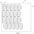
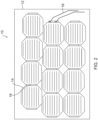
- FIGS. 1 and 2 illustrate conventional structures for solar cell panels 10, which include a substrate 12, a plurality of solar cells 14 arranged in an array, and electrical connectors 16 between the solar cells 14.
- Half size solar cells 14 are shown in FIG. 1 and full size solar cells 14 are shown in FIG. 2 .
- Space solar cells 14 are derived from a round Germanium (Ge) substrate starting material, which is later fabricated into semi-rectangular shapes to improve dense packing onto the solar cell panel 10. This wafer is often diced into one or two solar cells 14 herein described as half size or full size solar cells 14.
- the electrical connectors 16 providing electrical connections between solar cells 14 are made along the long parallel edge between solar cells 14. These series connections (cell-to-cell) are completed off-substrate, as strings of connected solar cells 14 are built having lengths of any number of solar cells 14. The completed strings of solar cells 14 are then applied and attached to the substrate 12.
- wiring 18 is attached at the end of a string of solar cells 14 to electrically connect the string to other strings, or to terminate the resulting circuit and bring the current off of the array of solar cells 14.
- String-to-string and circuit termination connections are typically done on the substrate 12, and typically using wiring 18.
- some solar cell panels 10 use a printed circuit board (PCB)-type material with embedded conductors.
- PCB printed circuit board
- Adjacent strings of connected solar cells 14 can run parallel or anti-parallel.
- strings of connected solar cells 14 can be aligned or misaligned. There are many competing influences to the solar cell 14 layout resulting in regions where solar cells 14 are parallel or anti-parallel, aligned or misaligned.
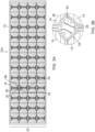
- FIGS. 3A-3B illustrate improved devices and structures for a solar cell panel 10a, according to one example, wherein FIG. 3B is an enlarged view of the details in the dashed circle in FIG. 3A .
- the various components of the solar cell panel 10a are shown and described in greater detail in FIGS. 5-13 .
- the solar cell panel 10a includes a substrate 12 for solar cells 14 having one or more corner conductors 20 thereon.
- the substrate 12 is a multi-layer substrate 12 comprised of one or more Kapton ® (polyimide) layers separating one or more patterned metal layers.
- Kapton ® polyimide
- the substrate 12 may be mounted on a large rigid panel 10a similar to conventional assembles. Alternatively, substrate 12 can be mounted to a lighter more sparse frame or panel 10a for mounting or deployment.
- a plurality of solar cells 14 are attached to the substrate 12 in a two-dimensional (2D) grid of an array 22.
- the array 22 is comprised of ninety-six (96) solar cells 14 arranged in four (4) rows by twenty-four (24) columns, but it is recognized that any number of solar cells 14 may be used in different implementations.
- At least one of the solar cells 14 has at least one cropped corner 24 that defines a corner region 26, as indicated by the dashed circle.
- the solar cells 14 are attached to the substrate 12, such that corner regions 26 of adjacent ones of the solar cells 14 are aligned, thereby exposing an area 28 of the substrate 12.
- the area 28 of the substrate 12 that is exposed includes one or more of the corner conductors 20, and one or more electrical connections between the solar cells 14 and the corner conductors 20 are made in the corner regions 26 resulting from the cropped corners 24 of the solar cells 14.
- the corner conductors 20 are conductive paths attached to, printed on, buried in, or deposited on the substrate 12, before and/or after the solar cells 14 are attached to the substrate 12, which facilitate connections between adjacent solar cells 14.
- the connections between the solar cells 14 and the corner conductors 20 are made after the solar cells 14 have been attached to the substrate 12.
- solar cells 14 are aligned on the substrate 12, such that four cropped corners 24, one from each solar cell 14, are brought together at the corner regions 26.
- the solar cells 14 are then individually attached to the substrate 12, wherein the solar cells 14 are placed on top of the corner conductors 20 to make the electrical connection between the solar cells 14 and the corner conductors 20.
- the solar cells 14 can be applied to the substrate 12 as CIC (cell, interconnect and coverglass) units.
- CIC cell, interconnect and coverglass
- bare solar cells 14 can be assembled on the substrate 12, and then interconnects applied to the solar cells 14, followed by the application of a single solar cell 14 coverglass, multiple solar cell 14 coverglass, multiple solar cell 14 polymer coversheet, or spray encapsulation. This assembly protects the solar cells 14 from damage that would limit performance.
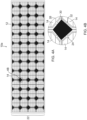
- FIGS. 4A and 4B illustrate an alternative structure for the solar cell panel 10a, according to one example, wherein FIG. 4B is an enlarged view of the details in the dashed circle in FIG. 4A .
- FIG. 4B is an enlarged view of the details in the dashed circle in FIG. 4A .
- PRM power routing module
- FIG. 5 illustrates the front side of an exemplary solar cell 14 that can be used in the improved solar cell panel 10a of FIGS. 3A-3B and 4A-4B .
- the solar cell 14, which is a CIC unit, is a half-size solar cell 14. (Full-size solar cells 14 could also be used.)
- the solar cell 14 is fabricated having at least one cropped corner 24 that defines a corner region 26, as indicated by the dashed circle, such that the corner region 26 resulting from the cropped corner 24 includes at least one contact 32, 34 for making an electrical connection to the solar cell 14.
- the solar cell 14 has two cropped corners 24, each of which has both a front contact 32 on the front side of the solar cell 14 and a back contact 34 on a back side of the solar cell 14, where the contacts 32 and 34 extend into the corner region 26.
- Full-size solar cells 14 would have four cropped corners 24, each of which would have a front contact 32 and a back contact 34.
- the cropped corners 24 increase utilization of the round wafer starting materials for the solar cells 14. In conventional panels 10, these cropped corners 24 would result in unused space on the panel 10 after the solar cells 14 are attached to the substrate 12.
- the new approach described in this disclosure utilizes this unused space. Specifically, metal foil interconnects, comprising the corner conductors 20, front contacts 32 and back contacts 34, are moved to the corner regions 26.
- existing CICs have interconnects attached to the solar cell 14 front side, and connect to the back side (where connections occur) during stringing.
- the current generated by the solar cell 14 is collected on the front side of the solar cell 14 by a grid 36 of thin metal fingers 38 and wider metal bus bars 40 that are connected to both of the front contacts 32.
- the bus bar 40 is a low resistance conductor that carries high currents and also provides redundancy should a front contact 32 become disconnected. Optimization generally desires a short bus bar 40 running directly between the front contacts 32. Having the front contact 32 in the cropped corner 24 results in moving the bus bar 40 away from the perimeter of the solar cell 14. This is achieved while simultaneously minimizing the bus bar 40 length and light obscuration.
- the fingers 38 are now shorter. This reduces parasitic resistances in the grid 36, because the length of the fingers 38 is shorter and the total current carried is less. This produces a design preference where the front contacts 32 and connecting bus bar 40 is moved to provide shorter narrow fingers 38.
- FIG. 6 illustrates the back side of the exemplary solar cell 14 of FIG. 5 .
- the back side of the solar cell 14 has a back layer 42 that is connected to both of the back contacts 34.
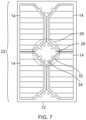
- FIG. 7 illustrates solar cells 14 arranged into the 2D grid of the array 22, according to one example.
- the array 22 comprises a plurality of solar cells 14 attached to a substrate 12, such that corner regions 26 of adjacent ones of the solar cells 14 are aligned, thereby exposing an area 28 of the substrate 12. Electrical connections (not shown) between the solar cells 14 are made in the exposed area 28 of the substrate 12 using the front contacts 32 and back contacts 34 of the solar cells 14 and corner conductors 20 (not shown) formed on or in the exposed area 28 of the substrate 12.
- the solar cells 14 are individually attached to the substrate 12. This assembly can be done directly on a support surface, i.e., the substrate 12, which can be either rigid or flexible. Alternatively, the solar cells 14 could be assembled into the 2D grid of the array 22 on a temporary support surface and then transferred to a final support surface, i.e., the substrate 12.
- FIG. 8 illustrates an example of the array 22 where one or more bypass diodes 44 are added to the exposed area 28 of the substrate 12 in the corner regions 26, for use in one or more of the electrical connections.
- the bypass diodes 44 protect the solar cells 14 when the solar cells 14 become unable to generate current, which could be due to being partially shadowed, which drives the solar cells 14 into reverse bias.
- the bypass diodes 44 are attached to the substrate 12 in the corner regions 26 independent of the solar cells 14.
- FIG. 9 illustrates an example where the bypass diode 44 is applied to the back side of the solar cell 14, with interconnects or contacts 46 for the bypass diode 44, one of which extends into the corner region 26 between the front and back contacts 32, 34.
- FIG. 10 illustrates a front side view of the example of FIG. 9 , with the interconnect or contact 46 for the bypass diode 44 (not shown) extending into the corner region 26 between the front and back contacts 32, 34.
- FIG. 11 illustrates the solar cells 14 of FIGS. 9 and 10 arranged into the 2D grid of the array 22 and applied to the substrate 12, where the bypass diodes 44 (not shown) are applied to the back side of the solar cells 14, with the contacts 46 for the bypass diodes 44 extending into the corner regions 26 of the solar cells 14.
- FIGS. 7 , 8 and 11 are generalized layouts. Specifically, these layouts can be repeated across any panel 10a dimensions desired by a customer. This greatly simplifies assembly, rework, test, and inspection processes.
- Front and back contacts 32, 34 of the solar cells 14 are present in each corner region 26 for attachment to the corner conductors 20.
- Interconnects for the front and back contacts 32, 34 of each of the solar cells 14 are welded, soldered, or otherwise bonded onto the corner conductors 20 to provide a conductive path 20, 32, 34 for routing current out of the solar cells 14.
- Adjacent solar cells 14 can be electrically connected to flow current in up/down or left/right directions as desired by the specific design. Current flow can also be routed around stayout zones as needed.
- the length or width of the solar cell array 22 can be set as desired. Also, the width can vary over the length of the array 22.
- the electrical connections are series connections that determine a flow of current through the plurality of solar cells 14. This may be accomplished by the connection schemes shown in FIGS. 12 and 13 , wherein FIG. 12 shows up/down series connections 48 between the solar cells 14 of the array 22, and FIG. 13 shows left/right series connections 50 between the solar cells 14 of the array 22.
- these series connections 48, 50 are electrical connections between the front contacts 32 and back contacts 34 of the solar cells 14, and the bypass diodes 44, are made using the corner conductors 20 formed on or in the exposed areas 28 of the substrate 12.
- These series connections 48, 50 determine the current (power) flow, as indicated by the arrows 52, through the solar cells 14, in contrast to the assembly of large strings off-substrate.
- the corner conductors 20 between solar cells 14 can be in many forms. They could be accomplished using wires that have electrical connections made on both ends, which could be from soldering, welding, conducting adhesive, or other process. In addition to wires, metal foil connectors, similar to the interconnects, could be applied. Metal conductive paths or traces (not shown) can also be integrated with the substrate 12.
- this new approach attaches the solar cells 14 individually to a substrate 12 such that the corner regions 26 of two, three or four adjacent solar cells 14 are aligned on the substrate 12.
- the solar cells 14 are laid out so that the cropped corners 24 are aligned and the corner regions 26 are adjacent, thereby exposing an area 28 of the substrate 12.
- Electrical connections between solar cells 14 are made in these corner regions 26 between front contacts 32 and back contacts 34 on the solar cells 14, bypass diodes 44, and corner conductors 20 on or in the exposed area 28 of the substrate 12, wherein these conductive paths are used to create a string of solar cells 14 in a series connection 48, 50 comprising a circuit.
- This disclosure describes the PRM 30 for customizing the corner conductors 20 used in the corner regions 26, wherein the PRM 30 is attached to the substrate 12 in the corner regions 26. Rather than form all of the corner conductors 20 on the substrate 12, most of the corner conductors 20 are contained within the PRM 30. Different versions of the PRM 30 having different conductor 20 layouts (e.g., 2D or 3D) can be selected to produce the desired connection layout for the array 22.
- FIG. 14 is a schematic side view of an example with a substrate 12 below and a PRM 30 above, wherein the substrate 12 is a flex sheet assembly, according to one example.
- the substrate 12 includes a polyimide base layer 54 with Copper (Cu) layer 56a above and Cu layer 56b below, wherein Cu layers 56a and 56b form a multilayer conductor.
- the Cu layer 56a is patterned as the corner conductors 20, and the Cu layer 56b is patterned to form buried conductors within the substrate 12, including, for example, V+, V-, and bridging lines.
- a conducting back sheet of polyimide 58 can be applied to the substrate 12, which is useful in a space environment in that it will reduce the accumulation of charge.
- the solar cell 14 Shown on the right side is the solar cell 14 that is attached to the substrate 12 with adhesive 60. Also visible is the metal foil interconnect 62 attached to the solar cell 14 and the corner conductors 20.
- the substrate 12 also includes insulating layers that separate at least one of the multilayer conductors 56a, 56b from at least another one of the multilayer conductors 56a, 56b.
- insulating layers that separate at least one of the multilayer conductors 56a, 56b from at least another one of the multilayer conductors 56a, 56b.
- Polyimide has a high breakdown strength, greater than air or vacuum, and the polyimide overlay layers 64a, 64b are useful for preventing ESD, which is an important concern in a space environment.
- the PRM 30 is positioned above the substrate 12 for electrically interconnecting the solar cells 14 in the array 22.
- the PRM 30 is comprised of an insulation layer comprising a polyimide base layer 64 and an electrically conductive layer comprising a single Cu layer 66 deposited thereon.
- the Cu layer 66 which comprises one or more corner conductors 20, is used for electrically interconnecting the solar cells 14, and the polyimide base layer 64 is used for electrically insulating the corner conductors 20 of the Cu layer 66.
- the base layer 64 of the PRM 30 is shown as being polyimide, it could be chosen from a wide variety of insulators that are suitable in the use environment, including other suitable polymers, as well as ceramics, such as glass or alumina.
- An advantage of glass or other transparent insulators is that these could be used with a laser welding process, where the laser beam is transmitted through the insulator and the laser beam's energy is absorbed by the conductive layer 66 on the PRM 30.
- the top (sun facing side) of the PRM 30 could have a highly reflective coating, such as an Al foil bonded to the polyimide. This will reflect the solar energy away reducing heating of the solar array 22 and reducing the solar cells 14 operating temperature, which will increase power generation.
- the PRM 30 may include a bypass diode 44 for protecting the solar cells 14 from a reverse bias, wherein the bypass diode 44 is connected to one or more of the corner conductors 20 of the PRM 30 by an interconnect 62.
- the PRM 30 may also include an adhesive 68 for attaching the PRM 30 to the substrate 12 and an electrical joint 70 for connecting one or more of the corner conductors 20 of the PRM 30 to one or more of corner conductors 20 of the substrate 12.
- FIG. 15 is a schematic side view of the example from FIG. 14 , with the PRM 30 attached to the substrate 12 using the adhesive 68.
- the PRM 30 is attached to the substrate 12 in the area 28 of the substrate 12 in the corner region 26 that remains exposed.
- an electrical connection is formed by the electrical joint 70 sandwiched between one or more of the corner conductors 20 of the PRM 30 and one or more of corner conductors 20 of the substrate 12, e.g., between the Cu layers 56a and 66.
- the electrical joint 70 could be accomplished with solder, via a laser welding process as described above, or via an ultrasonic welding process.
- FIG. 16 shows a top view of the corner regions 26 of the solar cells 14 in the array 22, including the front and back contacts 32, 34, without the PRM 30 attached. There are fewer corner conductors 20 shown in this view. Also, the area 28 of the substrate 12 in the corner region 26 that remains exposed includes conducting pads 72 that provide connection points between the PRM 30 and conductive paths in the substrate 12, e.g., power lines, bridging lines or other conductive paths buried or embedded within the substrate 12 (i.e., Cu layer 56b). This is a common design for all corner regions 26 independent of application and PRM 30.
- FIG. 17 shows one example where the PRM 30 electrically interconnects the solar cells 14 by providing a series connection 48 between the solar cells 14. Note that FIG. 17 shows the structure from the sun's perspective, looking through the polyimide base layer 64 (not shown) (the same is true for FIGS. 18 , 20 , 21 , 23 and 24 ). Corner conductor 20a connects to the back contact 34 of the top left solar cell 14 (not shown), corner conductor 20b connects to the front contact 32 of the bottom left solar cell 14 (not shown), and corner conductor 20c connects to the back contact 34 of the bottom left solar cell 14 (not shown) through bypass diode 44a.
- Corner conductor 20d connects to the back contact 34 of the bottom right solar cell 14 (not shown), corner conductor 20e connects to the front contact 32 of the top right solar cell 14 (not shown), and corner conductor 20f connects to the back contact 34 of the top right solar cell 14 (not shown) through bypass diode 44b.
- the PRMs 30 can be rotated to change the functionality of the connections between solar cells 14.
- the PRM 30 of FIG. 17 could be rotated to provide a left/right series connection 50.
- FIG. 18 shows another example where the PRM 30 electrically interconnects the solar cells 14 with one or more power lines in the substrate 12.
- corner conductor 20a terminates the back contact 34 of the top left solar cell 14 (not shown) to pads 72 for a buried power+ line (not shown)
- corner conductor 20b terminates the front contact 32 of the bottom left solar cell 14 (not shown) to pads 72 for a buried power-(common) line (not shown)
- corner conductor 20c connects to the back contact 34 of the bottom left solar cell 14 (not shown) through bypass diode 44a.
- Both corner conductors 20a, 20b have dual redundant connections to the pads 72 for the power+ and power- lines, although the number of connections could be increased or decreased if desired. Similar to FIG.
- corner conductor 20d connects to the back contact 34 of the bottom right solar cell 14 (not shown)
- corner conductor 20e connects to the front contact 32 of the top right solar cell 14 (not shown)
- corner conductor 20f connects to the back contact 34 of the top right solar cell 14 (not shown) through bypass diode 44b.
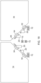
- FIG. 19 shows the layout for adjacent solar cells 14 at the bottom of a column in the array 22 before the PRM 30 is attached, including corner conductors 20, corner regions 26, front and back contacts 32, 34, and conducting pads 72 associated with power lines, bridging lines or other conductive paths buried or embedded within the substrate 12.
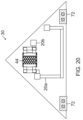
- FIG. 20 shows an example where the PRM 30 electrically interconnects the solar cells 14 between columns of the solar cells 14 in FIG. 19 .
- corner conductor 20a connects the back contact 34 of the left solar cell 14 (not shown) to the front contact 32 of the right solar cell 14 (not shown), and corner conductor 20b connects to the back contact 34 of the right solar cell 14 (not shown) through bypass diode 44.
- FIG. 21 shows another example where the PRM 30 electrically interconnects the solar cells 14 between columns of the solar cells 14 in FIG. 19 .
- corner conductor 20a terminates the back contact 34 of the left solar cell 14 (not shown) to a pad 72 for a buried power+ line (not shown)
- corner conductor 20b terminates the front contact 32 of the right solar cell 14 (not shown) to a pad 72 for buried power- (common) line (not shown)
- corner conductor 20c connects to the back contact 34 of the right solar cell 14 (not shown) through bypass diode 44.
- Only the corner conductor 20a has dual redundant connections to the pad 72 for the power+ line, although the number of connections could be increased or decreased if desired.
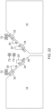
- FIG. 22 shows the layout for adjacent solar cells 14 at the top of a column in the array 22 before the PRM 30 is attached, including corner conductors 20, corner regions 26, front and back contacts 32, 34, and conducting pads 72 associated with power lines, bridging lines or other conductive paths buried or embedded within the substrate 12.
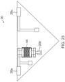
- FIG. 23 shows an example where the PRM 30 electrically interconnects the solar cells 14 between columns of the solar cells 14 in FIG. 22 .
- corner conductor 20a terminates the front contact 34 of the left solar cell 14 (not shown) to a pad 72 for a buried power- (common) line (not shown)
- corner conductor 20b connects to the back contact 34 of the left solar cell 14 (not shown) through bypass diode 44
- corner conductor 20c terminates the back contact 34 of the right solar cell 14 (not shown) to a pad 72 for a buried power- (common) line (not shown).
- This layout for the PRM 30 bridges the current from column-to-column in the array 22.
- FIG. 24 shows another example where the PRM 30 electrically interconnects the solar cells 14 between columns of the solar cells 14 in FIG. 22 .
- corner conductor 20a terminates the front contact 34 of the left solar cell 14 (not shown) to a pad 72 for a buried power+ line (not shown)
- corner conductor 20b connects to the back contact 34 of the left solar cell 14 (not shown) through bypass diode 44
- corner conductor 20c terminates the back contact 34 of the right solar cell 14 (not shown) to a pad 72 for a buried power- (common) line (not shown).
- FIG. 25 shows the layout for an array 22 comprised of four (4) rows by eight (8) columns of solar cells 14, labeled as Cell 1 14 through Cell 32 14, with the numbering of the solar cell 14 labels corresponding to the direction of the current as determined by the PRMs 30 electrically interconnecting the solar cells 14 within columns of the solar cells 14.
- the PRMs 30 for the third/fourth, fifth/sixth, and seventh/eighth columns of the first row work in conjunction with the PRMs 30 in the first/second and fifth/sixth columns of the second row to terminate circuits between solar cells 14.
- the PRMs 30 in the bottom row bridge the current between the columns.
- FIG. 26 shows the layout of FIG. 25 with Cell 12 14, Cell 13 14, Cell 19 14, Cell 20 14, Cell 21 14, Cell 22 14, Cell 26 14, Cell 27 14, Cell 28 14, Cell 29 14, Cell 30 14 and Cell 31 14 removed, and the bottom PRMs 30 moved up to terminate the third/fourth, fifth/sixth, and seventh/eighth columns, in order to form a non-rectangular array 22 of solar cells 14 using the PRMs 30 to electrically interconnect the solar cells 14 in the non-rectangular array 22.
- FIG. 27 shows the layout of FIG. 25 with Cell 10 14, Cell 1 14, Cell 12 14, Cell 13 14, Cell 14 14, Cell 15 14, Cell 18 14, Cell 19 14, Cell 20 14, Cell 21 14, Cell 22 14, Cell 23 14 removed, and the bottom PRMs 30 moved up to terminate the third/fourth and fifth/sixth columns and electrically interconnect the solar cells 14 by bridging connections around the removed solar cells 14, in order to define a stayout zone 74
- the PRM 30 includes one or more corner conductors 20 for enabling the stayout zone 74, wherein current flows through bridge lines embedded within the substrate 12 (i.e., Cu layer 56b).
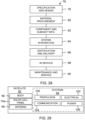
- Examples of the disclosure may be described in the context of a method 76 of fabricating a solar cell 14, solar cell panel 10a and/or satellite, comprising steps 78-90, as shown in FIG. 28 , wherein the resulting satellite 92 having a solar cell panel 10a comprised of solar cells 14 are shown in FIG. 29 .
- exemplary method 76 may include specification and design 78 of the solar cell 14, solar cell panel 10a and/or satellite 92, and material procurement 80 for same.
- component and subassembly manufacturing 82 and system integration 84 of the solar cell 14, solar cell panel 10a and/or satellite 92 takes place, which include fabricating the solar cell 14, solar cell panel 10a and/or satellite 92.
- the solar cell 14, solar cell panel 10a and/or satellite 92 may go through certification and delivery 86 in order to be placed in service 88.
- the solar cell 14, solar cell panel 10a and/or satellite 92 may also be scheduled for maintenance and service 90 (which includes modification, reconfiguration, refurbishment, and so on), before being launched.
- a system integrator may include without limitation any number of solar cell, solar cell panel, satellite or spacecraft manufacturers and major-system subcontractors;
- a third party may include without limitation any number of venders, subcontractors, and suppliers; and
- an operator may be a satellite company, military entity, service organization, and so on.
- a satellite 92 fabricated by exemplary method 76 may include systems 94, a body 96, solar cell panels 10a comprised of solar cells 14, and one or more antennae 98.
- the systems 94 included with the satellite 92 include, but are not limited to, one or more of a propulsion system 100, an electrical system 102, a communications system 104, and a power system 106. Any number of other systems 94 also may be included.
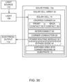
- FIG. 30 is an illustration of the solar cell panel 10a in the form of a functional block diagram, according to one example.
- the solar cell panel 10a is comprised of the solar cell array 22, which is comprised of one or more of the solar cells 14 individually attached to the substrate 12.
- Each of the solar cells 14 absorbs light 108 from a light source 110 and generates an electrical output 112 in response thereto.
- At least one of the solar cells 14 has at least one cropped corner 24 that defines a corner region 26, such that an area 28 of the substrate 12 remains exposed when the solar cell 14 is attached to the substrate 12.
- the corner regions 26 of adjacent ones of the solar cells 14 are aligned, thereby exposing the area 28 of the substrate 12.
- the area 28 of the substrate 12 that remains exposed includes one or more corner conductors 20 attached to, printed on, or integrated with the substrate 12, and one or more electrical connections between the solar cells 14 and the corner conductors 20 are made in a corner region 26.
- the corner region 26 may also include one or more bypass diodes 44.
- the corner region 26 includes at least one contact, for example, a front contact 32 on a front side of the solar cell 14 and/or a back contact 34 on a back side of the solar cell 14.
- An interconnect 62 is used for making the electrical connections between the solar cell 14 and the corner conductors 20.
- a power routing module 30 is attached to the exposed area 28 of the substrate 12 for electrically interconnecting solar cells 14 in the array 22, wherein the power routing module 30 includes a base layer 64, serving as an insulation layer, and an electrically conductive layer 66, the electrically conductive layer 66 is a conductor 20 for electrically interconnecting the solar cells 14, and the insulation layer 64 is used for electrically insulating the electrically conductive layer 66.
- the power routing module 30 may also include one or more bypass diodes 44, as well as an interconnect 62 connecting the bypass diode 44 to the electrically conductive layer 66.
Landscapes
- Photovoltaic Devices (AREA)
- Life Sciences & Earth Sciences (AREA)
- Engineering & Computer Science (AREA)
- Sustainable Energy (AREA)
- Sustainable Development (AREA)
- Chemical & Material Sciences (AREA)
- Materials Engineering (AREA)
- Nanotechnology (AREA)
Abstract
Description
- The disclosure is related generally to solar cell panels and, more specifically, to a power routing module for a solar cell array.
- Typical spaceflight-capable solar cell panel assembly involves building long strings of solar cells. These strings are variable in length and can be very long, for example, up to and greater than 20 cells. Assembling such long, variable, and fragile materials is difficult, which has prevented automation of the assembly.
- Existing solutions use solar cells assembled into CIC (cell, interconnect and coverglass) units. The CIC has metal foil interconnects connected to the front of the cell that extend in parallel from one side of the CIC. The CICs are located close to each other and the interconnects make connection to the bottom of an adjacent cell. Using these interconnects, the CICs are assembled into linear strings. These linear strings are built-up manually and then laid out to form a large solar cell array comprised of many strings of variable length.
- Additionally, a bypass diode is used to protect the cells from reverse bias, when the cells become partially shadowed. The bypass diode generally connects the back contacts of two adjacent cells within the solar cell array.
- When used in a satellite, the solar cell array is typically packaged as a panel. The dimensions of the panel are dictated by the needs of the satellite, including such constraints as needed power, as well as the size and shape necessary to pack and store the satellite in a launch vehicle. Furthermore, the deployment of the panel often requires that some portions of the panel are used for the mechanical fixtures and the solar cell array must avoid these locations. In practice, the panel is generally rectangular, but its dimensions and aspect ratio vary greatly. The layout of the CICs and strings to fill this space must be highly customized for maximum power generation, which results in a fabrication process that is highly manual.
- What is needed, then, is a means for promoting automated manufacturing of solar arrays, while preserving the ability for customization of solar cell arrays.
- The devices and methods of the present disclosure are exemplified in many ways, including, but not limited to, the following examples listed below.
- 1. Electrically interconnecting solar cells in an array using a power routing module, wherein the power routing module includes: an electrically conductive layer for electrically interconnecting the solar cells; and an insulation layer for electrically insulating the electrically conductive layer. At least one of the solar cells has at least one cropped corner that defines a corner region. An area of a substrate in the corner region remains exposed when the solar cells are attached to the substrate, and the power routing module is attached to the substrate in the area of the substrate in the corner region that remains exposed.
- 2. The electrically conductive layer of the power routing module is comprised of one or more conductors.
- 3. The power routing module includes a bypass diode for protecting the solar cells from a reverse bias, wherein the bypass diode is connected to one or more of the conductors of the power routing module.
- 4. The area of the substrate in the corner region that remains exposed includes conducting pads that provide connection points between the power routing module and conductive paths in the substrate.
- 5. An electrical connection is formed by an electrical joint sandwiched between one or more of the conductors of the power routing module and one or more of conductors of the substrate.
- 6. The power routing module electrically interconnects the solar cells with one or more power lines in the substrate.
- 7. The power routing module electrically interconnects the solar cells by providing a series connection between the solar cells.
- 8. The power routing module electrically interconnects the solar cells by bridging connections around the solar cells.
- 9. The power routing module electrically interconnects the solar cells within columns of the solar cells.
- 10. The power routing module electrically interconnects the solar cells between columns of the solar cells.
- 11. The array is a non-rectangular array and the power routing module electrically interconnects the solar cells in the non-rectangular array.
- 12. The power routing module includes one or more conductors for enabling a stayout zone.
- 13. The power routing module includes an adhesive for attaching to the substrate.
- Referring now to the drawings in which like reference numbers represent corresponding parts throughout:
-
FIGS. 1 and2 illustrate conventional structures for solar cell panels. -
FIGS. 3A and 3B illustrate an improved structure for a solar cell panel, according to one example. -
FIGS. 4A and 4B illustrate an alternative structure for the solar cell panel, according to one example. -
FIG. 5 illustrates the front side of an exemplary solar cell that may be used in the improved solar cell panel ofFIGS. 3A-3B and4A-4B . -
FIG. 6 illustrates the back side of the exemplary solar cell ofFIG. 5 . -
FIG. 7 illustrates cells arranged into a two-dimensional (2D) grid of an array, according to one example. -
FIG. 8 illustrates an example of the array where one or more bypass diodes are added to the exposed area of the substrate in the corner regions. -
FIG. 9 illustrates an example where the bypass diode is applied to the back side of the cell, with an interconnect or contact for the bypass diode extending into the corner region between front and back contacts. -
FIG. 10 illustrates a front side view of the example ofFIG. 9 , with the interconnect or contact for the bypass diode extending into the corner region between the front and back contacts. -
FIG. 11 illustrates the cells ofFIGS. 9 and10 arranged into the 2D grid of the array and applied to the substrate, where the bypass diodes are applied to the back side of the cells, with the contacts for the bypass diodes extending into the corner regions of the cells. -
FIG. 12 shows up/down series connections between the cells of the array, according to one example. -
FIG. 13 shows left/right series connections between the cells of the array, according to one example. -
FIG. 14 is a schematic side view of an example with a substrate below and a power routing module above, wherein the substrate is a flex sheet assembly. -
FIG. 15 is a schematic side view of an example with a substrate below and a power routing module above, with the power routing module attached to the flex sheet with an adhesive. -
FIG. 16 is a top view of a corner region of solar cells in an array. -
FIG. 17 shows the power routing module's structure for a series connection of the solar cells. -
FIG. 18 shows a variation of the power routing module attached to the solar cells in the array. -
FIG. 19 shows the layout for adjacent solar cells at the bottom of a column in the array before the power routing module is attached -
FIG. 20 shows an example of the power routing module that connects between the solar cells inFIG. 19 . -
FIG. 21 shows another example of the power routing module that connects between the solar cells inFIG. 19 . -
FIG. 22 shows the layout for adjacent solar cells at the top of a column in the array before the power routing module is attached. -
FIG. 23 shows an example of the power routing module that connects between the solar cells inFIG. 22 . -
FIG. 24 shows another example of the power routing module that connects between the solar cells inFIG. 22 . -
FIG. 25 shows the of an array of cells with the layout corresponding to the direction of the current as determined by the power routing modules. -
FIG. 26 shows the layout ofFIG. 25 with cells removed, and the bottom power routing modules moved, in order to form a non-rectangular array of solar cells using the power routing modules. -
FIG. 27 shows the layout ofFIG. 25 with cells removed, and the bottom power routing modules moved, in order to define a stayout zone. -
FIG. 28 describes a method of fabricating a solar cell, solar cell panel and/or satellite, according to one example. -
FIG. 29 illustrates a resulting satellite having a solar cell panel comprised of solar cells, according to one example. -
FIG. 30 is an illustration of the solar cell panel in the form of a functional block diagram, according to one example. - In the following description, reference is made to the accompanying drawings which form a part hereof, and in which is shown by way of illustration a specific example in which the disclosure may be practiced. It is to be understood that other examples may be utilized and structural changes may be made without departing from the scope of the present disclosure.
- A new approach to the design of solar cell arrays, such as those used for spaceflight power applications, is based on electrical connections among the solar cells in the array.
- This new approach rearranges the components of a solar cell and the arrangements of the solar cells in the array. Instead of having solar cells connected into long linear strings and then assembled onto a substrate, the solar cells are attached individually to a substrate, such that corner regions of adjacent cells are aligned on the substrate, thereby exposing an area of the substrate. Electrical connections between cells are made by corner conductors formed on or in the substrate in these corner regions. Consequently, this approach presents a solar cell array design based on individual cells.
- Thus, a single laydown process and layout can be used in the fabrication of solar cell arrays. Current flow between solar cells will be assisted with conductors embedded in the substrate. These electrical connections define the specific characteristics of the solar cell array, such as its dimensions, stayout zones, and circuit terminations. This approach simplifies manufacturing, enables automation, and reduces costs and delivery times.
-
FIGS. 1 and2 illustrate conventional structures forsolar cell panels 10, which include asubstrate 12, a plurality ofsolar cells 14 arranged in an array, andelectrical connectors 16 between thesolar cells 14. Half sizesolar cells 14 are shown inFIG. 1 and full sizesolar cells 14 are shown inFIG. 2 . Spacesolar cells 14 are derived from a round Germanium (Ge) substrate starting material, which is later fabricated into semi-rectangular shapes to improve dense packing onto thesolar cell panel 10. This wafer is often diced into one or twosolar cells 14 herein described as half size or full sizesolar cells 14. Theelectrical connectors 16 providing electrical connections betweensolar cells 14 are made along the long parallel edge betweensolar cells 14. These series connections (cell-to-cell) are completed off-substrate, as strings of connectedsolar cells 14 are built having lengths of any number ofsolar cells 14. The completed strings ofsolar cells 14 are then applied and attached to thesubstrate 12. - In
FIG. 2 , wiring 18 is attached at the end of a string ofsolar cells 14 to electrically connect the string to other strings, or to terminate the resulting circuit and bring the current off of the array ofsolar cells 14. String-to-string and circuit termination connections are typically done on thesubstrate 12, and typically usingwiring 18. However, somesolar cell panels 10 use a printed circuit board (PCB)-type material with embedded conductors. - Adjacent strings of connected
solar cells 14 can run parallel or anti-parallel. In addition, strings of connectedsolar cells 14 can be aligned or misaligned. There are many competing influences to thesolar cell 14 layout resulting in regions wheresolar cells 14 are parallel or anti-parallel, aligned or misaligned. -
FIGS. 3A-3B illustrate improved devices and structures for asolar cell panel 10a, according to one example, whereinFIG. 3B is an enlarged view of the details in the dashed circle inFIG. 3A . The various components of thesolar cell panel 10a are shown and described in greater detail inFIGS. 5-13 . - The
solar cell panel 10a includes asubstrate 12 forsolar cells 14 having one ormore corner conductors 20 thereon. In one example, thesubstrate 12 is amulti-layer substrate 12 comprised of one or more Kapton® (polyimide) layers separating one or more patterned metal layers. Thesubstrate 12 may be mounted on a largerigid panel 10a similar to conventional assembles. Alternatively,substrate 12 can be mounted to a lighter more sparse frame orpanel 10a for mounting or deployment. - A plurality of
solar cells 14 are attached to thesubstrate 12 in a two-dimensional (2D) grid of anarray 22. In this example, thearray 22 is comprised of ninety-six (96)solar cells 14 arranged in four (4) rows by twenty-four (24) columns, but it is recognized that any number ofsolar cells 14 may be used in different implementations. - At least one of the
solar cells 14 has at least one croppedcorner 24 that defines acorner region 26, as indicated by the dashed circle. Thesolar cells 14 are attached to thesubstrate 12, such thatcorner regions 26 of adjacent ones of thesolar cells 14 are aligned, thereby exposing anarea 28 of thesubstrate 12. Thearea 28 of thesubstrate 12 that is exposed includes one or more of thecorner conductors 20, and one or more electrical connections between thesolar cells 14 and thecorner conductors 20 are made in thecorner regions 26 resulting from the croppedcorners 24 of thesolar cells 14. - In this example, the
corner conductors 20 are conductive paths attached to, printed on, buried in, or deposited on thesubstrate 12, before and/or after thesolar cells 14 are attached to thesubstrate 12, which facilitate connections between adjacentsolar cells 14. The connections between thesolar cells 14 and thecorner conductors 20 are made after thesolar cells 14 have been attached to thesubstrate 12. - Four adjacent
solar cells 14 are aligned on thesubstrate 12, such that four croppedcorners 24, one from eachsolar cell 14, are brought together at thecorner regions 26. Thesolar cells 14 are then individually attached to thesubstrate 12, wherein thesolar cells 14 are placed on top of thecorner conductors 20 to make the electrical connection between thesolar cells 14 and thecorner conductors 20. - The
solar cells 14 can be applied to thesubstrate 12 as CIC (cell, interconnect and coverglass) units. Alternatively, baresolar cells 14 can be assembled on thesubstrate 12, and then interconnects applied to thesolar cells 14, followed by the application of a singlesolar cell 14 coverglass, multiplesolar cell 14 coverglass, multiplesolar cell 14 polymer coversheet, or spray encapsulation. This assembly protects thesolar cells 14 from damage that would limit performance. -
FIGS. 4A and 4B illustrate an alternative structure for thesolar cell panel 10a, according to one example, whereinFIG. 4B is an enlarged view of the details in the dashed circle inFIG. 4A . In this example, only afew corner conductors 20 are printed on or integrated with thesubstrate 12. Instead, most of thecorner conductors 20 are contained within a power routing module (PRM) 30 that is attached to thesubstrate 12, as described in more detail below in conjunction withFIGS. 14-27 . -
FIG. 5 illustrates the front side of an exemplarysolar cell 14 that can be used in the improvedsolar cell panel 10a ofFIGS. 3A-3B and4A-4B . Thesolar cell 14, which is a CIC unit, is a half-sizesolar cell 14. (Full-sizesolar cells 14 could also be used.) - The
solar cell 14 is fabricated having at least one croppedcorner 24 that defines acorner region 26, as indicated by the dashed circle, such that thecorner region 26 resulting from the croppedcorner 24 includes at least onecontact solar cell 14. In the example ofFIG. 5 , thesolar cell 14 has two croppedcorners 24, each of which has both afront contact 32 on the front side of thesolar cell 14 and aback contact 34 on a back side of thesolar cell 14, where thecontacts corner region 26. (Full-sizesolar cells 14 would have four croppedcorners 24, each of which would have afront contact 32 and aback contact 34.) - The cropped
corners 24 increase utilization of the round wafer starting materials for thesolar cells 14. Inconventional panels 10, these croppedcorners 24 would result in unused space on thepanel 10 after thesolar cells 14 are attached to thesubstrate 12. The new approach described in this disclosure, however, utilizes this unused space. Specifically, metal foil interconnects, comprising thecorner conductors 20,front contacts 32 andback contacts 34, are moved to thecorner regions 26. In contrast, existing CICs have interconnects attached to thesolar cell 14 front side, and connect to the back side (where connections occur) during stringing. - The current generated by the
solar cell 14 is collected on the front side of thesolar cell 14 by agrid 36 ofthin metal fingers 38 and wider metal bus bars 40 that are connected to both of thefront contacts 32. There is a balance between the addition of metal ingrid 36, which reduces the light entering thesolar cell 14 and its output power, and the reduced resistance of having more metal. Thebus bar 40 is a low resistance conductor that carries high currents and also provides redundancy should afront contact 32 become disconnected. Optimization generally desires ashort bus bar 40 running directly between thefront contacts 32. Having thefront contact 32 in the croppedcorner 24 results in moving thebus bar 40 away from the perimeter of thesolar cell 14. This is achieved while simultaneously minimizing thebus bar 40 length and light obscuration. Additionally, thefingers 38 are now shorter. This reduces parasitic resistances in thegrid 36, because the length of thefingers 38 is shorter and the total current carried is less. This produces a design preference where thefront contacts 32 and connectingbus bar 40 is moved to provide shorternarrow fingers 38. -
FIG. 6 illustrates the back side of the exemplarysolar cell 14 ofFIG. 5 . The back side of thesolar cell 14 has aback layer 42 that is connected to both of theback contacts 34. -
FIG. 7 illustratessolar cells 14 arranged into the 2D grid of thearray 22, according to one example. Thearray 22 comprises a plurality ofsolar cells 14 attached to asubstrate 12, such thatcorner regions 26 of adjacent ones of thesolar cells 14 are aligned, thereby exposing anarea 28 of thesubstrate 12. Electrical connections (not shown) between thesolar cells 14 are made in the exposedarea 28 of thesubstrate 12 using thefront contacts 32 andback contacts 34 of thesolar cells 14 and corner conductors 20 (not shown) formed on or in the exposedarea 28 of thesubstrate 12. - During assembly, the
solar cells 14 are individually attached to thesubstrate 12. This assembly can be done directly on a support surface, i.e., thesubstrate 12, which can be either rigid or flexible. Alternatively, thesolar cells 14 could be assembled into the 2D grid of thearray 22 on a temporary support surface and then transferred to a final support surface, i.e., thesubstrate 12. -
FIG. 8 illustrates an example of thearray 22 where one ormore bypass diodes 44 are added to the exposedarea 28 of thesubstrate 12 in thecorner regions 26, for use in one or more of the electrical connections. Thebypass diodes 44 protect thesolar cells 14 when thesolar cells 14 become unable to generate current, which could be due to being partially shadowed, which drives thesolar cells 14 into reverse bias. In one example, thebypass diodes 44 are attached to thesubstrate 12 in thecorner regions 26 independent of thesolar cells 14. -
FIG. 9 illustrates an example where thebypass diode 44 is applied to the back side of thesolar cell 14, with interconnects orcontacts 46 for thebypass diode 44, one of which extends into thecorner region 26 between the front andback contacts -
FIG. 10 illustrates a front side view of the example ofFIG. 9 , with the interconnect or contact 46 for the bypass diode 44 (not shown) extending into thecorner region 26 between the front andback contacts -
FIG. 11 illustrates thesolar cells 14 ofFIGS. 9 and10 arranged into the 2D grid of thearray 22 and applied to thesubstrate 12, where the bypass diodes 44 (not shown) are applied to the back side of thesolar cells 14, with thecontacts 46 for thebypass diodes 44 extending into thecorner regions 26 of thesolar cells 14. - One advantage of this approach is that the layouts illustrated in
FIGS. 7 ,8 and11 are generalized layouts. Specifically, these layouts can be repeated across anypanel 10a dimensions desired by a customer. This greatly simplifies assembly, rework, test, and inspection processes. - Following
solar cell 14 andbypass diode 44 placement, there is another step where customization is accomplished. Thefront contacts 32 andback contacts 34 in thecorner regions 26 of thesolar cells 14 must be connected. This can be done in many combinations in order to route current through a desired path. - After attaching
solar cells 14 to thesubstrate 12, connections are made between thesolar cells 14 and thecorner conductors 20. Front andback contacts solar cells 14 are present in eachcorner region 26 for attachment to thecorner conductors 20. Interconnects for the front andback contacts solar cells 14 are welded, soldered, or otherwise bonded onto thecorner conductors 20 to provide aconductive path solar cells 14. - Using the
corner conductors 20, any customization can be made in the electrical connections. Adjacentsolar cells 14 can be electrically connected to flow current in up/down or left/right directions as desired by the specific design. Current flow can also be routed around stayout zones as needed. The length or width of thesolar cell array 22 can be set as desired. Also, the width can vary over the length of thearray 22. - In one example, the electrical connections are series connections that determine a flow of current through the plurality of
solar cells 14. This may be accomplished by the connection schemes shown inFIGS. 12 and13 , whereinFIG. 12 shows up/downseries connections 48 between thesolar cells 14 of thearray 22, andFIG. 13 shows left/right series connections 50 between thesolar cells 14 of thearray 22. In bothFIGS. 12 and13 , theseseries connections front contacts 32 andback contacts 34 of thesolar cells 14, and thebypass diodes 44, are made using thecorner conductors 20 formed on or in the exposedareas 28 of thesubstrate 12. Theseseries connections arrows 52, through thesolar cells 14, in contrast to the assembly of large strings off-substrate. - The
corner conductors 20 betweensolar cells 14 can be in many forms. They could be accomplished using wires that have electrical connections made on both ends, which could be from soldering, welding, conducting adhesive, or other process. In addition to wires, metal foil connectors, similar to the interconnects, could be applied. Metal conductive paths or traces (not shown) can also be integrated with thesubstrate 12. - In summary, this new approach attaches the
solar cells 14 individually to asubstrate 12 such that thecorner regions 26 of two, three or four adjacentsolar cells 14 are aligned on thesubstrate 12. Thesolar cells 14 are laid out so that the croppedcorners 24 are aligned and thecorner regions 26 are adjacent, thereby exposing anarea 28 of thesubstrate 12. Electrical connections betweensolar cells 14 are made in thesecorner regions 26 betweenfront contacts 32 andback contacts 34 on thesolar cells 14,bypass diodes 44, andcorner conductors 20 on or in the exposedarea 28 of thesubstrate 12, wherein these conductive paths are used to create a string ofsolar cells 14 in aseries connection - While the use of electrical connections between
solar cells 14 in thecorner regions 26 facilitates automation, there is still a need for a variety ofcorner conductors 20 that can achieve various configurations to enable the customization needed by customers. However, this may requiremany corner conductors 20 in thecorner regions 26, which would result incorner conductors 20 being closely spaced, raising electrostatic discharge (ESD) concerns. - On the other hand, to maximize power generation from the array of
solar cells 14, it is desirable to havecorner regions 26 as small as possible. Largesolar cells 14 are also desirable for reducing labor and parts cost during assembly. - However, the design described herein changes this assessment, with the result that smaller
solar cells 14 have little cost penalty. Smallersolar cells 14 have advantages in filling the wafer area, as well as filling thepanels 10a. Smallersolar cells 14 mean better utilization of material and effort. However, smallersolar cells 14 also mean smaller croppedcorners 24 andsmaller corner regions 26, which causes problems for the connection strategy. - This disclosure describes the
PRM 30 for customizing thecorner conductors 20 used in thecorner regions 26, wherein thePRM 30 is attached to thesubstrate 12 in thecorner regions 26. Rather than form all of thecorner conductors 20 on thesubstrate 12, most of thecorner conductors 20 are contained within thePRM 30. Different versions of thePRM 30 havingdifferent conductor 20 layouts (e.g., 2D or 3D) can be selected to produce the desired connection layout for thearray 22. -
FIG. 14 is a schematic side view of an example with asubstrate 12 below and aPRM 30 above, wherein thesubstrate 12 is a flex sheet assembly, according to one example. Thesubstrate 12 includes apolyimide base layer 54 with Copper (Cu)layer 56a above andCu layer 56b below, wherein Cu layers 56a and 56b form a multilayer conductor. TheCu layer 56a is patterned as thecorner conductors 20, and theCu layer 56b is patterned to form buried conductors within thesubstrate 12, including, for example, V+, V-, and bridging lines. A conducting back sheet ofpolyimide 58 can be applied to thesubstrate 12, which is useful in a space environment in that it will reduce the accumulation of charge. - Shown on the right side is the
solar cell 14 that is attached to thesubstrate 12 withadhesive 60. Also visible is themetal foil interconnect 62 attached to thesolar cell 14 and thecorner conductors 20. - The
substrate 12 also includes insulating layers that separate at least one of themultilayer conductors multilayer conductors polyimide overlay layer 64a and bottompolyimide overlay layer 64b. Polyimide has a high breakdown strength, greater than air or vacuum, and thepolyimide overlay layers - The
PRM 30 is positioned above thesubstrate 12 for electrically interconnecting thesolar cells 14 in thearray 22. ThePRM 30 is comprised of an insulation layer comprising apolyimide base layer 64 and an electrically conductive layer comprising asingle Cu layer 66 deposited thereon. TheCu layer 66, which comprises one ormore corner conductors 20, is used for electrically interconnecting thesolar cells 14, and thepolyimide base layer 64 is used for electrically insulating thecorner conductors 20 of theCu layer 66. - While the
base layer 64 of thePRM 30 is shown as being polyimide, it could be chosen from a wide variety of insulators that are suitable in the use environment, including other suitable polymers, as well as ceramics, such as glass or alumina. An advantage of glass or other transparent insulators is that these could be used with a laser welding process, where the laser beam is transmitted through the insulator and the laser beam's energy is absorbed by theconductive layer 66 on thePRM 30. - The top (sun facing side) of the
PRM 30 could have a highly reflective coating, such as an Al foil bonded to the polyimide. This will reflect the solar energy away reducing heating of thesolar array 22 and reducing thesolar cells 14 operating temperature, which will increase power generation. - The
PRM 30 may include abypass diode 44 for protecting thesolar cells 14 from a reverse bias, wherein thebypass diode 44 is connected to one or more of thecorner conductors 20 of thePRM 30 by aninterconnect 62. ThePRM 30 may also include an adhesive 68 for attaching thePRM 30 to thesubstrate 12 and an electrical joint 70 for connecting one or more of thecorner conductors 20 of thePRM 30 to one or more ofcorner conductors 20 of thesubstrate 12. -
FIG. 15 is a schematic side view of the example fromFIG. 14 , with thePRM 30 attached to thesubstrate 12 using the adhesive 68. ThePRM 30 is attached to thesubstrate 12 in thearea 28 of thesubstrate 12 in thecorner region 26 that remains exposed. In this example, an electrical connection is formed by the electrical joint 70 sandwiched between one or more of thecorner conductors 20 of thePRM 30 and one or more ofcorner conductors 20 of thesubstrate 12, e.g., between the Cu layers 56a and 66. The electrical joint 70 could be accomplished with solder, via a laser welding process as described above, or via an ultrasonic welding process. -
FIG. 16 shows a top view of thecorner regions 26 of thesolar cells 14 in thearray 22, including the front andback contacts PRM 30 attached. There arefewer corner conductors 20 shown in this view. Also, thearea 28 of thesubstrate 12 in thecorner region 26 that remains exposed includes conductingpads 72 that provide connection points between thePRM 30 and conductive paths in thesubstrate 12, e.g., power lines, bridging lines or other conductive paths buried or embedded within the substrate 12 (i.e.,Cu layer 56b). This is a common design for allcorner regions 26 independent of application andPRM 30. -
FIG. 17 shows one example where thePRM 30 electrically interconnects thesolar cells 14 by providing aseries connection 48 between thesolar cells 14. Note thatFIG. 17 shows the structure from the sun's perspective, looking through the polyimide base layer 64 (not shown) (the same is true forFIGS. 18 ,20 ,21 ,23 and24 ).Corner conductor 20a connects to theback contact 34 of the top left solar cell 14 (not shown),corner conductor 20b connects to thefront contact 32 of the bottom left solar cell 14 (not shown), andcorner conductor 20c connects to theback contact 34 of the bottom left solar cell 14 (not shown) throughbypass diode 44a.Corner conductor 20d connects to theback contact 34 of the bottom right solar cell 14 (not shown),corner conductor 20e connects to thefront contact 32 of the top right solar cell 14 (not shown), andcorner conductor 20f connects to theback contact 34 of the top right solar cell 14 (not shown) throughbypass diode 44b. - Note that, with minor modifications, the
PRMs 30 can be rotated to change the functionality of the connections betweensolar cells 14. For example, thePRM 30 ofFIG. 17 could be rotated to provide a left/right series connection 50. -
FIG. 18 shows another example where thePRM 30 electrically interconnects thesolar cells 14 with one or more power lines in thesubstrate 12. In this example,corner conductor 20a terminates theback contact 34 of the top left solar cell 14 (not shown) topads 72 for a buried power+ line (not shown),corner conductor 20b terminates thefront contact 32 of the bottom left solar cell 14 (not shown) topads 72 for a buried power-(common) line (not shown), andcorner conductor 20c connects to theback contact 34 of the bottom left solar cell 14 (not shown) throughbypass diode 44a. Bothcorner conductors pads 72 for the power+ and power- lines, although the number of connections could be increased or decreased if desired. Similar toFIG. 17 ,corner conductor 20d connects to theback contact 34 of the bottom right solar cell 14 (not shown),corner conductor 20e connects to thefront contact 32 of the top right solar cell 14 (not shown), andcorner conductor 20f connects to theback contact 34 of the top right solar cell 14 (not shown) throughbypass diode 44b. -
FIG. 19 shows the layout for adjacentsolar cells 14 at the bottom of a column in thearray 22 before thePRM 30 is attached, includingcorner conductors 20,corner regions 26, front andback contacts pads 72 associated with power lines, bridging lines or other conductive paths buried or embedded within thesubstrate 12. -
FIG. 20 shows an example where thePRM 30 electrically interconnects thesolar cells 14 between columns of thesolar cells 14 inFIG. 19 . In this example,corner conductor 20a connects theback contact 34 of the left solar cell 14 (not shown) to thefront contact 32 of the right solar cell 14 (not shown), andcorner conductor 20b connects to theback contact 34 of the right solar cell 14 (not shown) throughbypass diode 44. -
FIG. 21 shows another example where thePRM 30 electrically interconnects thesolar cells 14 between columns of thesolar cells 14 inFIG. 19 . In this example,corner conductor 20a terminates theback contact 34 of the left solar cell 14 (not shown) to apad 72 for a buried power+ line (not shown),corner conductor 20b terminates thefront contact 32 of the right solar cell 14 (not shown) to apad 72 for buried power- (common) line (not shown), andcorner conductor 20c connects to theback contact 34 of the right solar cell 14 (not shown) throughbypass diode 44. Only thecorner conductor 20a has dual redundant connections to thepad 72 for the power+ line, although the number of connections could be increased or decreased if desired. -
FIG. 22 shows the layout for adjacentsolar cells 14 at the top of a column in thearray 22 before thePRM 30 is attached, includingcorner conductors 20,corner regions 26, front andback contacts pads 72 associated with power lines, bridging lines or other conductive paths buried or embedded within thesubstrate 12. -
FIG. 23 shows an example where thePRM 30 electrically interconnects thesolar cells 14 between columns of thesolar cells 14 inFIG. 22 . In this example,corner conductor 20a terminates thefront contact 34 of the left solar cell 14 (not shown) to apad 72 for a buried power- (common) line (not shown),corner conductor 20b connects to theback contact 34 of the left solar cell 14 (not shown) throughbypass diode 44, andcorner conductor 20c terminates theback contact 34 of the right solar cell 14 (not shown) to apad 72 for a buried power- (common) line (not shown). This layout for thePRM 30 bridges the current from column-to-column in thearray 22. -
FIG. 24 shows another example where thePRM 30 electrically interconnects thesolar cells 14 between columns of thesolar cells 14 inFIG. 22 . In this example,corner conductor 20a terminates thefront contact 34 of the left solar cell 14 (not shown) to apad 72 for a buried power+ line (not shown),corner conductor 20b connects to theback contact 34 of the left solar cell 14 (not shown) throughbypass diode 44, andcorner conductor 20c terminates theback contact 34 of the right solar cell 14 (not shown) to apad 72 for a buried power- (common) line (not shown). -
FIG. 25 shows the layout for anarray 22 comprised of four (4) rows by eight (8) columns ofsolar cells 14, labeled as Cell 1 14 throughCell 32 14, with the numbering of thesolar cell 14 labels corresponding to the direction of the current as determined by thePRMs 30 electrically interconnecting thesolar cells 14 within columns of thesolar cells 14. ThePRMs 30 for the third/fourth, fifth/sixth, and seventh/eighth columns of the first row work in conjunction with thePRMs 30 in the first/second and fifth/sixth columns of the second row to terminate circuits betweensolar cells 14. ThePRMs 30 in the bottom row bridge the current between the columns. -
FIG. 26 shows the layout ofFIG. 25 withCell 12 14,Cell 13 14, Cell 19 14,Cell 20 14, Cell 21 14,Cell 22 14,Cell 26 14, Cell 27 14,Cell 28 14, Cell 29 14,Cell 30 14 and Cell 31 14 removed, and thebottom PRMs 30 moved up to terminate the third/fourth, fifth/sixth, and seventh/eighth columns, in order to form anon-rectangular array 22 ofsolar cells 14 using thePRMs 30 to electrically interconnect thesolar cells 14 in thenon-rectangular array 22. -
FIG. 27 shows the layout ofFIG. 25 withCell 10 14, Cell 1 14,Cell 12 14,Cell 13 14,Cell 14 14, Cell 15 14,Cell 18 14, Cell 19 14,Cell 20 14, Cell 21 14,Cell 22 14, Cell 23 14 removed, and thebottom PRMs 30 moved up to terminate the third/fourth and fifth/sixth columns and electrically interconnect thesolar cells 14 by bridging connections around the removedsolar cells 14, in order to define astayout zone 74 ThePRM 30 includes one ormore corner conductors 20 for enabling the stayoutzone 74, wherein current flows through bridge lines embedded within the substrate 12 (i.e.,Cu layer 56b). - Examples of the disclosure may be described in the context of a
method 76 of fabricating asolar cell 14,solar cell panel 10a and/or satellite, comprising steps 78-90, as shown inFIG. 28 , wherein the resultingsatellite 92 having asolar cell panel 10a comprised ofsolar cells 14 are shown inFIG. 29 . - As illustrated in
FIG. 28 , during pre-production,exemplary method 76 may include specification anddesign 78 of thesolar cell 14,solar cell panel 10a and/orsatellite 92, andmaterial procurement 80 for same. During production, component andsubassembly manufacturing 82 andsystem integration 84 of thesolar cell 14,solar cell panel 10a and/orsatellite 92 takes place, which include fabricating thesolar cell 14,solar cell panel 10a and/orsatellite 92. Thereafter, thesolar cell 14,solar cell panel 10a and/orsatellite 92 may go through certification anddelivery 86 in order to be placed inservice 88. Thesolar cell 14,solar cell panel 10a and/orsatellite 92 may also be scheduled for maintenance and service 90 (which includes modification, reconfiguration, refurbishment, and so on), before being launched. - Each of the processes of
method 76 may be performed or carried out by a system integrator, a third party, and/or an operator (e.g., a customer). For the purposes of this description, a system integrator may include without limitation any number of solar cell, solar cell panel, satellite or spacecraft manufacturers and major-system subcontractors; a third party may include without limitation any number of venders, subcontractors, and suppliers; and an operator may be a satellite company, military entity, service organization, and so on. - As shown in
FIG. 29 , asatellite 92 fabricated byexemplary method 76 may includesystems 94, abody 96,solar cell panels 10a comprised ofsolar cells 14, and one ormore antennae 98. Examples of thesystems 94 included with thesatellite 92 include, but are not limited to, one or more of apropulsion system 100, anelectrical system 102, a communications system 104, and apower system 106. Any number ofother systems 94 also may be included. -
FIG. 30 is an illustration of thesolar cell panel 10a in the form of a functional block diagram, according to one example. Thesolar cell panel 10a is comprised of thesolar cell array 22, which is comprised of one or more of thesolar cells 14 individually attached to thesubstrate 12. Each of thesolar cells 14 absorbs light 108 from alight source 110 and generates anelectrical output 112 in response thereto. - At least one of the
solar cells 14 has at least one croppedcorner 24 that defines acorner region 26, such that anarea 28 of thesubstrate 12 remains exposed when thesolar cell 14 is attached to thesubstrate 12. When a plurality ofsolar cells 14 are attached to thesubstrate 12, thecorner regions 26 of adjacent ones of thesolar cells 14 are aligned, thereby exposing thearea 28 of thesubstrate 12. - The
area 28 of thesubstrate 12 that remains exposed includes one ormore corner conductors 20 attached to, printed on, or integrated with thesubstrate 12, and one or more electrical connections between thesolar cells 14 and thecorner conductors 20 are made in acorner region 26. Thecorner region 26 may also include one ormore bypass diodes 44. - The
corner region 26 includes at least one contact, for example, afront contact 32 on a front side of thesolar cell 14 and/or aback contact 34 on a back side of thesolar cell 14. - An
interconnect 62 is used for making the electrical connections between thesolar cell 14 and thecorner conductors 20. - A
power routing module 30 is attached to the exposedarea 28 of thesubstrate 12 for electrically interconnectingsolar cells 14 in thearray 22, wherein thepower routing module 30 includes abase layer 64, serving as an insulation layer, and an electricallyconductive layer 66, the electricallyconductive layer 66 is aconductor 20 for electrically interconnecting thesolar cells 14, and theinsulation layer 64 is used for electrically insulating the electricallyconductive layer 66. Thepower routing module 30 may also include one ormore bypass diodes 44, as well as aninterconnect 62 connecting thebypass diode 44 to the electricallyconductive layer 66. - Further, the disclosure comprises embodiments according to the following clauses:
- Clause 1. A device, comprising: a power routing module for electrically interconnecting solar cells in an array, wherein the power routing module includes: an electrically conductive layer for electrically interconnecting the solar cells; and an insulation layer for electrically insulating the electrically conductive layer; wherein at least one of the solar cells has at least one cropped corner that defines a corner region; wherein an area of a substrate in the corner region remains exposed when the solar cells are attached to the substrate; and wherein the power routing module is attached to the substrate in the area of the substrate in the corner region that remains exposed.
- Clause 2. The device of Clause 1, wherein the electrically conductive layer of the power routing module is comprised of one or more conductors.
- Clause 3. The device of Clause 2, wherein the power routing module includes a bypass diode for protecting the solar cells from a reverse bias and the bypass diode is connected to one or more of the conductors of the power routing module.
- Clause 4. The device of Clause 2 or 3, wherein an electrical connection is formed by an electrical joint sandwiched between one or more of the conductors of the power routing module and one or more of conductors of the substrate.
- Clause 5. The device of any one of Clauses 1-4, wherein the area of the substrate in the corner region that remains exposed includes conducting pads that provide connection points between the power routing module and conductive paths in the substrate.
- Clause 6. The device of any one of Clauses 1-5, wherein the power routing module electrically interconnects the solar cells with one or more power lines in the substrate.
- Clause 7. The device of any one of Clauses 1-6, wherein the power routing module electrically interconnects the solar cells by providing a series connection between the solar cells.
- Clause 8. The device of any one of Clauses 1-7, wherein the power routing module electrically interconnects the solar cells by bridging connections around the solar cells.
- Clause 9. The device of any one of Clauses 1-8, wherein the power routing module electrically interconnects the solar cells within columns of the solar cells.
-
Clause 10. The device of any one of Clauses 1-9, wherein the power routing module electrically interconnects the solar cells between columns of the solar cells. - Clause 11. The device of any one of Clauses 1-10, wherein the array is a non-rectangular array and the power routing module electrically interconnects the solar cells in the non-rectangular array.
-
Clause 12. The device of any one of Clauses 1-11, wherein the power routing module includes one or more conductors for enabling a stayout zone. -
Clause 13. The device of any one of Clauses 1-12, wherein the power routing module includes an adhesive for attaching to the substrate. -
Clause 14. A method, comprising: electrically interconnecting solar cells in an array using a power routing module, wherein the power routing module includes: an electrically conductive layer for electrically interconnecting the solar cells; and an insulation layer for electrically insulating the electrically conductive layer; wherein at least one of the solar cells has at least one cropped corner that defines a corner region; wherein an area of a substrate in the corner region remains exposed when the solar cells are attached to the substrate; and wherein the power routing module is attached to the substrate in the area of the substrate in the corner region that remains exposed. - Clause 15. The method of
Clause 14, wherein the electrically conductive layer of the power routing module is comprised of one or more conductors. -
Clause 16. The method of Clause 15, wherein the power routing module includes a bypass diode for protecting the solar cells from a reverse bias and the bypass diode is connected to one or more of the conductors of the power routing module. - Clause 17. The method of
Clause 15 or 16, wherein an electrical connection is formed by an electrical joint sandwiched between one or more of the conductors of the power routing module and one or more of conductors of the substrate. -
Clause 18. The method of any one of Clauses 14-17, wherein the area of the substrate in the corner region that remains exposed includes conducting pads that provide connection points between the power routing module and conductive paths in the substrate. - Clause 19. The method of any one of Clauses 14-18, wherein the power routing module electrically interconnects the solar cells with one or more power lines in the substrate.
-
Clause 20. The method of any one of Clauses 14-19, wherein the power routing module electrically interconnects the solar cells by providing a series connection between the solar cells. - Clause 21. The method of any one of Clauses 14-20, wherein the power routing module electrically interconnects the solar cells by bridging connections around the solar cells.
-
Clause 22. The method of any one of Clauses 14-21, wherein the power routing module electrically interconnects the solar cells within columns of the solar cells. - Clause 23. The method of any one of Clauses 14-22, wherein the power routing module electrically interconnects the solar cells between columns of the solar cells.
-
Clause 24. The method of any one of Clauses 14-23, wherein the array is a non-rectangular array and the power routing module electrically interconnects the solar cells in the non-rectangular array. - Clause 25. The method of any one of Clauses 14-24, wherein the power routing module includes one or more conductors for enabling a stayout zone.
-
Clause 26. The method of any one of Clauses 14-25, wherein the power routing module includes an adhesive for attaching to the substrate. - Clause 27. A solar cell panel, comprising: a solar cell array comprised of at least one power routing module for electrically interconnecting solar cells in the array, wherein the power routing module includes: an electrically conductive layer for electrically interconnecting the solar cells; and an insulation layer for electrically insulating the electrically conductive layer; wherein at least one of the solar cells has at least one cropped corner that defines a corner region; wherein an area of a substrate in the corner region remains exposed when the solar cells are attached to the substrate; and wherein the power routing module is attached to the substrate in the area of the substrate in the corner region that remains exposed.
-
Clause 28. The solar cell panel of Clause 27, wherein the electrically conductive layer of the power routing module is comprised of one or more conductors. - Clause 29. The solar cell panel of
Clause 28, wherein the power routing module includes a bypass diode for protecting the solar cells from a reverse bias and the bypass diode is connected to one or more of the conductors of the power routing module. -
Clause 30. The solar cell panel ofClause 28 or 29, wherein an electrical connection is formed by an electrical joint sandwiched between one or more of the conductors of the power routing module and one or more of conductors of the substrate. - Clause 31. The solar cell panel of any one of Clauses 27-30, wherein the area of the substrate in the corner region that remains exposed includes conducting pads that provide connection points between the power routing module and conductive paths in the substrate.
-
Clause 32. The solar cell panel of any one of Clauses 27-31, wherein the power routing module electrically interconnects the solar cells with one or more power lines in the substrate. - Clause 33. The solar cell panel of any one of Clauses 27-32, wherein the power routing module electrically interconnects the solar cells by providing a series connection between the solar cells.
-
Clause 34. The solar cell panel of any one of Clauses 27-33, wherein the power routing module electrically interconnects the solar cells by bridging connections around the solar cells. - Clause 35. The solar cell panel of any one of Clauses 27-34, wherein the power routing module electrically interconnects the solar cells within columns of the solar cells.
-
Clause 36. The solar cell panel of any one of Clauses 27-35, wherein the power routing module electrically interconnects the solar cells between columns of the solar cells. - Clause 37. The solar cell panel of any one of Clauses 27-36, wherein the array is a non-rectangular array and the power routing module electrically interconnects the solar cells in the non-rectangular array.
-
Clause 38. The solar cell panel of any one of Clauses 27-37, wherein the power routing module includes one or more conductors for enabling a stayout zone. - Clause 39. The solar cell panel of any one of Clauses 27-38, wherein the power routing module includes an adhesive for attaching to the substrate.
- The description of the examples set forth above has been presented for purposes of illustration and description, and is not intended to be exhaustive or limited to the examples described. Many alternatives, modifications and variations may be used in place of the specific elements described above.
Claims (13)
- A solar cell panel, comprising: a solar cell array comprised of at least one power routing module for electrically interconnecting solar cells in the array, wherein the power routing module includes: an electrically conductive layer for electrically interconnecting the solar cells; and an insulation layer for electrically insulating the electrically conductive layer; wherein at least one of the solar cells has at least one cropped corner that defines a corner region; wherein an area of a substrate in the corner region remains exposed when the solar cells are attached to the substrate; and wherein the power routing module is attached to the substrate in the area of the substrate in the corner region that remains exposed.
- The solar cell panel of claim 1, wherein the electrically conductive layer of the power routing module is comprised of one or more conductors.
- The solar cell panel of claim 2, wherein the power routing module includes a bypass diode for protecting the solar cells from a reverse bias and the bypass diode is connected to one or more of the conductors of the power routing module.
- The solar cell panel of claim 2 or 3, wherein an electrical connection is formed by an electrical joint sandwiched between one or more of the conductors of the power routing module and one or more of conductors of the substrate.
- The solar cell panel of any one of claims 1 to 4, wherein the area of the substrate in the corner region that remains exposed includes conducting pads that provide connection points between the power routing module and conductive paths in the substrate.
- The solar cell panel of any one of claims 1 to 5, wherein the power routing module electrically interconnects the solar cells with one or more power lines in the substrate.
- The solar cell panel of any one of claims 1 to 6, wherein the power routing module electrically interconnects the solar cells by providing a series connection between the solar cells.
- The solar cell panel of any one of claims 1 to 7, wherein the power routing module electrically interconnects the solar cells by bridging connections around the solar cells.
- The solar cell panel of any one of claims 1 to 8, wherein the power routing module electrically interconnects the solar cells within columns of the solar cells.
- The solar cell panel of any one of claims 1 to 9, wherein the power routing module electrically interconnects the solar cells between columns of the solar cells.
- The solar cell panel of any one of claims 1 to 10, wherein the array is a non-rectangular array and the power routing module electrically interconnects the solar cells in the non-rectangular array.
- The solar cell panel of any one of claims 1 to 11, wherein the power routing module includes one or more conductors for enabling a stayout zone.
- The solar cell panel of any one of claims 1 to 12, wherein the power routing module includes an adhesive for attaching to the substrate.
Applications Claiming Priority (20)
| Application Number | Priority Date | Filing Date | Title |
|---|---|---|---|
| US201662394666P | 2016-09-14 | 2016-09-14 | |
| US201662394616P | 2016-09-14 | 2016-09-14 | |
| US201662394671P | 2016-09-14 | 2016-09-14 | |
| US201662394623P | 2016-09-14 | 2016-09-14 | |
| US201662394627P | 2016-09-14 | 2016-09-14 | |
| US201662394629P | 2016-09-14 | 2016-09-14 | |
| US201662394641P | 2016-09-14 | 2016-09-14 | |
| US201662394649P | 2016-09-14 | 2016-09-14 | |
| US201662394636P | 2016-09-14 | 2016-09-14 | |
| US201662394672P | 2016-09-14 | 2016-09-14 | |
| US201662394632P | 2016-09-14 | 2016-09-14 | |
| US201662394667P | 2016-09-14 | 2016-09-14 | |
| US15/643,289 US11437533B2 (en) | 2016-09-14 | 2017-07-06 | Solar cells for a solar cell array |
| US15/643,274 US20180076346A1 (en) | 2016-09-14 | 2017-07-06 | Solar cell array connections using corner conductors |
| US15/643,285 US12696550B2 (en) | 2016-09-14 | 2017-07-06 | Power routing module with a switching matrix for a solar cell array |
| US15/643,279 US20180076348A1 (en) | 2016-09-14 | 2017-07-06 | Rework and repair of components in a solar cell array |
| US15/643,282 US20180076349A1 (en) | 2016-09-14 | 2017-07-06 | Power routing module for a solar cell array |
| US15/643,277 US12615851B2 (en) | 2016-09-14 | 2017-07-06 | Prefabricated conductors on a substrate to facilitate corner connections for a solar cell array |
| US15/643,287 US10763383B2 (en) | 2016-09-14 | 2017-07-06 | Nano-metal connections for a solar cell array |
| EP17191159.7A EP3297041B1 (en) | 2016-09-14 | 2017-09-14 | Power routing module for a solar cell array |
Related Parent Applications (2)
| Application Number | Title | Priority Date | Filing Date |
|---|---|---|---|
| EP17191159.7A Division EP3297041B1 (en) | 2016-09-14 | 2017-09-14 | Power routing module for a solar cell array |
| EP17191159.7A Division-Into EP3297041B1 (en) | 2016-09-14 | 2017-09-14 | Power routing module for a solar cell array |
Publications (3)
| Publication Number | Publication Date |
|---|---|
| EP4273940A2 true EP4273940A2 (en) | 2023-11-08 |
| EP4273940A3 EP4273940A3 (en) | 2023-12-13 |
| EP4273940B1 EP4273940B1 (en) | 2026-03-04 |
Family
ID=62149305
Family Applications (3)
| Application Number | Title | Priority Date | Filing Date |
|---|---|---|---|
| EP23169034.8A Pending EP4235815A3 (en) | 2016-09-14 | 2017-09-14 | Prefabricated conductors on a substrate to facilitate corner connections for a solar cell array |
| EP23178386.1A Pending EP4235810A3 (en) | 2016-09-14 | 2017-09-14 | Rework and repair of components in a solar cell array |
| EP23197851.1A Active EP4273940B1 (en) | 2016-09-14 | 2017-09-14 | Power routing module for a solar cell array |
Family Applications Before (2)
| Application Number | Title | Priority Date | Filing Date |
|---|---|---|---|
| EP23169034.8A Pending EP4235815A3 (en) | 2016-09-14 | 2017-09-14 | Prefabricated conductors on a substrate to facilitate corner connections for a solar cell array |
| EP23178386.1A Pending EP4235810A3 (en) | 2016-09-14 | 2017-09-14 | Rework and repair of components in a solar cell array |
Country Status (4)
| Country | Link |
|---|---|
| US (6) | US10763383B2 (en) |
| EP (3) | EP4235815A3 (en) |
| JP (12) | JP7411320B2 (en) |
| ES (3) | ES2970867T3 (en) |
Families Citing this family (17)
| Publication number | Priority date | Publication date | Assignee | Title |
|---|---|---|---|---|
| US10749051B1 (en) * | 2014-09-12 | 2020-08-18 | Solaero Technologies Corp. | Back contact solar cell assemblies |
| USD999723S1 (en) | 2014-10-15 | 2023-09-26 | Sunpower Corporation | Solar panel |
| USD913210S1 (en) * | 2014-10-15 | 2021-03-16 | Sunpower Corporation | Solar panel |
| US10763383B2 (en) * | 2016-09-14 | 2020-09-01 | The Boeing Company | Nano-metal connections for a solar cell array |
| DE112017007700B4 (en) * | 2017-06-30 | 2023-06-07 | Mitsubishi Electric Corporation | SOLAR POWER GENERATOR, SOLAR FIELD WINGS, SPATIAL STRUCTURE AND METHOD OF MANUFACTURING A SOLAR POWER GENERATOR |
| US10601367B2 (en) | 2018-05-11 | 2020-03-24 | The Boeing Company | System for redirecting sunlight to a mobile platform |
| CN111276549B (en) | 2018-11-20 | 2021-03-09 | 成都晔凡科技有限公司 | Cell for shingled assembly, shingled assembly, and method for making cell |
| KR102721329B1 (en) * | 2019-03-27 | 2024-10-23 | 주식회사 엘지화학 | Transparent light emitting device display |
| US11495701B2 (en) * | 2020-05-26 | 2022-11-08 | The Boeing Company | Conductive interconnect for connecting adjacent solar cells in a solar cell assembly |
| US11575056B1 (en) * | 2020-07-15 | 2023-02-07 | The Boeing Company | Repairing a solar cell bonded on a flexible circuit |
| US12040414B2 (en) * | 2020-08-11 | 2024-07-16 | The Boeing Company | Feed-through wiring solution for solar cell modules |
| US11722094B2 (en) * | 2020-08-21 | 2023-08-08 | The Boeing Company | Flexible circuit for solar cell assemblies |
| US11967661B1 (en) | 2021-01-27 | 2024-04-23 | Bae Systems Space & Mission Systems Inc. | Solar panel design and methods for magnetic cleanliness |
| US12107177B2 (en) | 2021-09-24 | 2024-10-01 | The Boeing Company | Lightweight flexible solar array |
| US20240039470A1 (en) * | 2022-07-29 | 2024-02-01 | Jonathan Jacques | Modular multi-panel solar cell |
| CN116632118B (en) * | 2023-07-18 | 2023-09-26 | 英利能源发展有限公司 | Preparation method of photovoltaic module |
| CN122248843A (en) * | 2026-05-13 | 2026-06-19 | 晶科能源(海宁)有限公司 | A back-contact solar cell, its preparation method, preparation equipment, and photovoltaic module. |
Family Cites Families (132)
| Publication number | Priority date | Publication date | Assignee | Title |
|---|---|---|---|---|
| DE1013644B (en) | 1955-01-14 | 1957-08-14 | Stamicarbon | Process for the production of coarse-grained urea |
| US3376164A (en) | 1963-08-01 | 1968-04-02 | Globe Union Inc | Photovoltaic power assembly |
| US3833426A (en) | 1973-11-08 | 1974-09-03 | Trw Inc | Solar array |
| US4057439A (en) | 1976-08-25 | 1977-11-08 | Solarex Corporation | Solar panel |
| US4257821A (en) | 1978-11-13 | 1981-03-24 | Trw Inc. | Universal solar cell/conductor junction element and solar panel embodying same |
| US4481378A (en) * | 1982-07-30 | 1984-11-06 | Motorola, Inc. | Protected photovoltaic module |
| JPS6167966A (en) * | 1984-09-11 | 1986-04-08 | Sharp Corp | Solar cell array |
| JPS61202474A (en) * | 1985-03-05 | 1986-09-08 | Mitsubishi Electric Corp | Solar battery array for space |
| US4755231A (en) * | 1986-06-13 | 1988-07-05 | Trw Inc. | Flexible solar array cell and substrate therefor |
| JPH0711475Y2 (en) * | 1988-09-30 | 1995-03-15 | 日本電気株式会社 | Solar cell |
| US5011544A (en) * | 1989-09-08 | 1991-04-30 | Solarex Corporation | Solar panel with interconnects and masking structure, and method |
| JPH04223378A (en) * | 1990-12-25 | 1992-08-13 | Sharp Corp | Solar cell |
| JP2912496B2 (en) | 1991-09-30 | 1999-06-28 | シャープ株式会社 | Solar cell module |
| US5391235A (en) | 1992-03-31 | 1995-02-21 | Canon Kabushiki Kaisha | Solar cell module and method of manufacturing the same |
| TW280962B (en) | 1995-02-24 | 1996-07-11 | Sanyo Electric Co | Battery charger and a solar battery used for charging a battery |
| US5567248A (en) | 1995-09-05 | 1996-10-22 | Chung; Darius | Modular solar cell contact arrangement |
| WO1999048136A2 (en) | 1998-03-13 | 1999-09-23 | Steffen Keller | Solar cell arrangement |
| US6156967A (en) * | 1998-06-04 | 2000-12-05 | Tecstar Power Systems, Inc. | Modular glass covered solar cell array |
| JP3602721B2 (en) * | 1998-06-12 | 2004-12-15 | 株式会社豊田自動織機 | Solar cell module |
| JP2000012885A (en) * | 1998-06-23 | 2000-01-14 | Honda Motor Co Ltd | Solar cell |
| DE19836272C2 (en) | 1998-08-11 | 2003-08-07 | Astrium Gmbh | Flexible, foldable solar generator for spacecraft |
| GB2341273A (en) | 1998-09-04 | 2000-03-08 | Eev Ltd | Solar cell arrangements |
| US6008448A (en) | 1998-10-15 | 1999-12-28 | Space Systems/Loral, Inc. | Solar panel array with stepped taper |
| US6034322A (en) | 1999-07-01 | 2000-03-07 | Space Systems/Loral, Inc. | Solar cell assembly |
| JP3748344B2 (en) * | 1999-10-12 | 2006-02-22 | ミサワホーム株式会社 | Solar panel |
| US6794725B2 (en) | 1999-12-21 | 2004-09-21 | Xerox Corporation | Amorphous silicon sensor with micro-spring interconnects for achieving high uniformity in integrated light-emitting sources |
| US6313396B1 (en) | 2000-05-22 | 2001-11-06 | The Boeing Company | Lightweight solar module and method of fabrication |
| US6350944B1 (en) | 2000-05-30 | 2002-02-26 | Hughes Electronics Corporation | Solar module array with reconfigurable tile |
| JP2002190612A (en) | 2000-12-22 | 2002-07-05 | Mitsubishi Electric Corp | Solar array panel and method of manufacturing the same |
| DE10136442A1 (en) | 2001-07-26 | 2003-02-13 | Ralf Adelhelm | Solar cell contact grid, collector and connector contact surfaces manufacture positions connector contact surfaces to allow maximum packing density of solar cells |
| ITMI20011653A1 (en) | 2001-07-30 | 2003-01-30 | Lorenzo Cerofolini | SOLAR CELL ELECTRIC POWER SUPPLY |
| US6555739B2 (en) | 2001-09-10 | 2003-04-29 | Ekla-Tek, Llc | Photovoltaic array and method of manufacturing same |
| US6637702B1 (en) | 2002-04-24 | 2003-10-28 | Lockheed Martin Corporation | Nested beam deployable solar array |
| JP2004241753A (en) * | 2002-12-13 | 2004-08-26 | Canon Inc | Solar cell module |
| JP3873889B2 (en) | 2003-01-16 | 2007-01-31 | 株式会社デンソー | Wire bonding method |
| FR2864347B1 (en) | 2003-12-23 | 2006-03-03 | Cit Alcatel | SOLAR GENERATOR PANEL AND ASSOCIATED SATELLITE |
| DE102004044061A1 (en) * | 2004-09-11 | 2006-04-20 | Rwe Space Solar Power Gmbh | Solar cell arrangement and method for interconnecting a solar cell string |
| US7245134B2 (en) | 2005-01-31 | 2007-07-17 | Formfactor, Inc. | Probe card assembly including a programmable device to selectively route signals from channels of a test system controller to probes |
| AU2006223474A1 (en) | 2005-03-11 | 2006-09-21 | Bp Corporation North America Inc. | Integrated solar cell roofing system and method of manufacture |
| KR100735395B1 (en) | 2005-05-10 | 2007-07-04 | 삼성전자주식회사 | Routing Method of Printed Circuit Board Using Integrated Circuit |
| US7514116B2 (en) | 2005-12-30 | 2009-04-07 | Intel Corporation | Horizontal Carbon Nanotubes by Vertical Growth and Rolling |
| US20140166067A1 (en) * | 2006-08-07 | 2014-06-19 | Emcore Solar Power, Inc. | Solar power system for aircraft, watercraft, or land vehicles using inverted metamorphic multijunction solar cells |
| US20080142071A1 (en) | 2006-12-15 | 2008-06-19 | Miasole | Protovoltaic module utilizing a flex circuit for reconfiguration |
| DE102007011403A1 (en) | 2007-03-08 | 2008-09-11 | Fraunhofer-Gesellschaft zur Förderung der angewandten Forschung e.V. | Front side series connected solar module |
| DE102007021843A1 (en) * | 2007-05-07 | 2008-11-13 | Leonhard Kurz Gmbh & Co. Kg | Photovoltaic module |
| JP2008282926A (en) | 2007-05-09 | 2008-11-20 | Sanyo Electric Co Ltd | Solar cell module |
| FR2917899B1 (en) | 2007-06-21 | 2010-05-28 | Apollon Solar | PHOTOVOLTAIC MODULE COMPRISING A POLYMERIC FILM AND METHOD OF MANUFACTURING SUCH MODULE |
| US20090025778A1 (en) | 2007-07-23 | 2009-01-29 | Day4 Energy Inc. | Shading protection for solar cells and solar cell modules |
| JP4819004B2 (en) * | 2007-08-10 | 2011-11-16 | シャープ株式会社 | Solar cell array and solar cell module |
| US20110041890A1 (en) * | 2007-11-19 | 2011-02-24 | Sheats James R | High-efficiency, high current solar cell and solar module |
| EP2068369A1 (en) * | 2007-12-03 | 2009-06-10 | Interuniversitair Microelektronica Centrum (IMEC) | Photovoltaic cells having metal wrap through and improved passivation |
| US8933320B2 (en) | 2008-01-18 | 2015-01-13 | Tenksolar, Inc. | Redundant electrical architecture for photovoltaic modules |
| US20090255571A1 (en) | 2008-04-14 | 2009-10-15 | Bp Corporation North America Inc. | Thermal Conducting Materials for Solar Panel Components |
| KR20110008284A (en) | 2008-04-29 | 2011-01-26 | 어플라이드 머티어리얼스, 인코포레이티드 | Photovoltaic Modules Manufactured Using Monolithic Module Assembly Technologies |
| US20090272436A1 (en) | 2008-05-05 | 2009-11-05 | Osbert Hay Cheung | Non-glass photovoltaic module and methods for manufacture |
| KR20090121629A (en) | 2008-05-22 | 2009-11-26 | 삼성전자주식회사 | Solar cell and solar cell module using same |
| CN201369335Y (en) * | 2008-10-15 | 2009-12-23 | 太聚能源股份有限公司 | Photovoltaic cell module |
| JP5064353B2 (en) | 2008-10-27 | 2012-10-31 | シャープ株式会社 | Solar cell device, portable electronic device, and global positioning system device |
| US20110168238A1 (en) | 2010-01-11 | 2011-07-14 | Solopower, Inc. | Flexible solar modules and manufacturing the same |
| US20100186795A1 (en) | 2009-01-28 | 2010-07-29 | Stephen Joseph Gaul | Connection systems and methods for solar cells |
| TW201032339A (en) | 2009-02-20 | 2010-09-01 | Aussmak Optoelectronic Corp | Solar cell |
| JP4915821B2 (en) | 2009-03-17 | 2012-04-11 | 独立行政法人産業技術総合研究所 | Solar power system |
| BRPI1012165A2 (en) | 2009-05-19 | 2019-04-02 | Maxout Renewables, Inc. | apparatus for balancing power output and power harvesting. |
| US20100313954A1 (en) | 2009-06-16 | 2010-12-16 | Emcore Solar Power, Inc. | Concentrated Photovoltaic System Receiver for III-V Semiconductor Solar Cells |
| EP2457259A2 (en) | 2009-07-22 | 2012-05-30 | Applied Materials, Inc. | Monolithic module assembly using back contact solar cells and metal ribbon |
| JP2011071214A (en) | 2009-09-24 | 2011-04-07 | Kaneka Corp | Solar cell module |
| US20110073163A1 (en) | 2009-09-25 | 2011-03-31 | Osbert Hay Cheung | Photovoltaic lamination and roof mounting systems |
| JP5459766B2 (en) * | 2009-10-01 | 2014-04-02 | Nec東芝スペースシステム株式会社 | Solar cell panel, method for suppressing electrification of solar cell panel, and solar power generator for artificial satellite |
| US9324885B2 (en) | 2009-10-02 | 2016-04-26 | Tigo Energy, Inc. | Systems and methods to provide enhanced diode bypass paths |
| JP2011108969A (en) | 2009-11-20 | 2011-06-02 | Hitachi Cable Ltd | Method of manufacturing solar cell module and wiring board for solar cell |
| WO2011084545A2 (en) | 2009-12-16 | 2011-07-14 | Nagendra Cherukupalli | Systems, circuits, and methods for reconfiguring solar cells of an adaptive solar power system |
| JP2011155041A (en) | 2010-01-26 | 2011-08-11 | Kyocera Corp | Solar cell element and solar cell module |
| US8469313B2 (en) | 2010-02-16 | 2013-06-25 | The Boeing Company | Aerodynamic structure having a ridged solar panel and an associated method |
| KR100965541B1 (en) | 2010-02-17 | 2010-06-23 | 아익시스코리아(주) | Solar cell module and manufacturing method thereof |
| JP2011210747A (en) | 2010-03-26 | 2011-10-20 | Mitsubishi Chemicals Corp | Solar cell module and method of manufacturing the same |
| WO2011142666A1 (en) | 2010-05-11 | 2011-11-17 | Stichting Energieonderzoek Centrum Nederland | Solar cell and method of manufacturing such a solar cell |
| JP2012043981A (en) * | 2010-08-19 | 2012-03-01 | National Institute Of Advanced Industrial & Technology | Solar cell module |
| NL2005261C2 (en) | 2010-08-24 | 2012-02-27 | Solland Solar Cells B V | Back contacted photovoltaic cell with an improved shunt resistance. |
| US8814099B1 (en) | 2010-08-31 | 2014-08-26 | MMA Design, LLC | Deployable morphing modular solar array |
| KR101091264B1 (en) * | 2010-09-10 | 2011-12-07 | 주식회사 디엠에스 | Dye-Sensitized Solar Cell Module |
| WO2012058053A2 (en) | 2010-10-29 | 2012-05-03 | Applied Materials, Inc. | Monolithic module assembly using back contact solar cells and metal ribbon |
| US20120125391A1 (en) | 2010-11-19 | 2012-05-24 | Solopower, Inc. | Methods for interconnecting photovoltaic cells |
| US8604330B1 (en) | 2010-12-06 | 2013-12-10 | 4Power, Llc | High-efficiency solar-cell arrays with integrated devices and methods for forming them |
| JP2012138518A (en) | 2010-12-27 | 2012-07-19 | Sony Corp | Photovoltaic power generation module and inspection method |
| KR20120091670A (en) | 2011-02-09 | 2012-08-20 | 엘지전자 주식회사 | Solar cell module and method of manufacturing the same |
| JP2012204651A (en) | 2011-03-25 | 2012-10-22 | Sharp Corp | Solar cell module, photovoltaic power generation system, connection switching control method for solar cell in solar cell module, connection switching control program, and recording medium |
| AT12996U1 (en) | 2011-06-07 | 2013-03-15 | Austria Tech & System Tech | PHOTOVOLTAIC MODULE AND USE THEREOF |
| US9252294B2 (en) | 2011-06-08 | 2016-02-02 | Andrew V. Latham | Instantaneous solar array recombining technology |
| NL1038916C2 (en) | 2011-07-01 | 2013-01-07 | Stichting Energie | Photovoltaic cell with wrap through connections. |
| EP2546889B1 (en) | 2011-07-12 | 2020-06-17 | Airbus Defence and Space GmbH | Solar cell assembly and method of fabrication of solar cell assembly |
| EP2752889B1 (en) * | 2011-08-31 | 2018-11-28 | Panasonic Intellectual Property Management Co., Ltd. | Method for producing solar cell module |
| US20130056047A1 (en) | 2011-09-02 | 2013-03-07 | Markus E. Beck | Photovoltaic module with sealed perimeter and method of formation |
| JP2013080788A (en) * | 2011-10-03 | 2013-05-02 | Sharp Corp | Solar cell module |
| US9768338B2 (en) | 2012-01-23 | 2017-09-19 | Stc.Unm | Multi-source optimal reconfigurable energy harvester |
| JP2013175624A (en) | 2012-02-27 | 2013-09-05 | Hitachi High-Technologies Corp | Production method of solar cell module and solar cell module assembly device |
| US9120583B1 (en) | 2012-03-01 | 2015-09-01 | Deployable Space Systems, Inc. | Space solar array architecture for ultra-high power applications |
| US9136412B2 (en) | 2012-03-11 | 2015-09-15 | Scuint Corporation | Reconfigurable solar panel |
| WO2013146414A1 (en) | 2012-03-30 | 2013-10-03 | 凸版印刷株式会社 | Back contact solar cell module |
| GB2501899A (en) | 2012-05-09 | 2013-11-13 | Itouchenergy Ltd | Solar cell module and systems |
| US8898970B2 (en) | 2012-06-12 | 2014-12-02 | Certainteed Corporation | Photovoltaic roofing systems with inner corner flashings |
| US20140000682A1 (en) * | 2012-06-27 | 2014-01-02 | E I Du Pont De Nemours And Company | Integrated back-sheet for back contact photovoltaic module |
| US9356173B2 (en) * | 2012-08-31 | 2016-05-31 | Sandia Corporation | Dynamically reconfigurable photovoltaic system |
| JP2014049724A (en) * | 2012-09-04 | 2014-03-17 | Sharp Corp | Solar cell module |
| DE102012217105A1 (en) | 2012-09-24 | 2014-04-17 | Robert Bosch Gmbh | Electric circuit and method for producing an electrical circuit |
| EP2907168B1 (en) | 2012-10-15 | 2017-06-07 | Pardell Vilella, Ricard | Cpvlis - concentration photovoltaics laminated interconnection system comprising a cpv receiver panel, a method for preparing the cpv receiver panel and an installation comprising the same |
| US9780253B2 (en) | 2014-05-27 | 2017-10-03 | Sunpower Corporation | Shingled solar cell module |
| KR20150125693A (en) | 2013-03-05 | 2015-11-09 | 시온 파워 코퍼레이션 | Electrochemical cells comprising fibril materials, such as fibril cellulose materials |
| CN203277428U (en) | 2013-04-12 | 2013-11-06 | 北京桑纳斯太阳能电池有限公司 | Solar cell module with PCB back board |
| TWM512217U (en) | 2013-06-20 | 2015-11-11 | Plant PV | Solar battery |
| US9627565B2 (en) | 2013-11-27 | 2017-04-18 | Space Systems/Loral, Llc | Integral corner bypass diode interconnecting configuration for multiple solar cells |
| US11302987B2 (en) | 2014-10-16 | 2022-04-12 | Lat Enterprises | Material for dissipating heat from and/or reducing heat signature of electronic devices and clothing |
| US20160112004A1 (en) | 2014-10-16 | 2016-04-21 | LAT Enterprises, Inc., d/b/a MediPak Energy Systems | Material for Dissipating Heat From and/or Reducing Heat Signature of Electronic Devices and Clothing |
| NL2012556B1 (en) | 2014-04-02 | 2016-02-15 | Stichting Energieonderzoek Centrum Nederland | Photovoltaic module with bypass diodes. |
| JP2015207598A (en) * | 2014-04-17 | 2015-11-19 | 三菱電機株式会社 | Solar cell module, solar cell, and inter-element connection body |
| US9818903B2 (en) * | 2014-04-30 | 2017-11-14 | Sunpower Corporation | Bonds for solar cell metallization |
| FR3024591B1 (en) | 2014-07-29 | 2016-08-05 | Bubendorff | METHOD FOR MANUFACTURING A PHOTOVOLTAIC PANEL |
| JP2016058455A (en) | 2014-09-05 | 2016-04-21 | 株式会社東芝 | Photoelectric conversion element, wiring board for photoelectric conversion element, manufacturing method of photoelectric conversion element, and photoelectric conversion structure |
| US20160126380A1 (en) | 2014-10-30 | 2016-05-05 | Sung Un CHANG | Flexible solar panel and method of fabricating the same |
| CN104443439A (en) | 2014-11-18 | 2015-03-25 | 上海空间电源研究所 | Folding cell-built-in flexible solar cell array |
| JP6422426B2 (en) * | 2014-12-09 | 2018-11-14 | 三菱電機株式会社 | Solar cell |
| US9758261B1 (en) | 2015-01-15 | 2017-09-12 | Solaero Technologies Corp. | Inverted metamorphic multijunction solar cell with lightweight laminate substrate |
| US20160218665A1 (en) | 2015-01-22 | 2016-07-28 | Solaero Technologies Corp. | Space solar cell panel with blocking diodes |
| CN204558477U (en) * | 2015-05-05 | 2015-08-12 | 中国人民解放军军械工程学院 | Surface has solar cell and the assembly thereof of the Internet trellis antistatic film |
| KR20170012123A (en) | 2015-07-24 | 2017-02-02 | 주식회사 엘지화학 | A process for manufacturing a flexible substrate |
| US20170040933A1 (en) | 2015-08-03 | 2017-02-09 | Grid+ Advisors, LLC | Photovoltiac nanogrid systems |
| US10097005B2 (en) | 2015-08-17 | 2018-10-09 | Solarcity Corporation | Self-configuring photo-voltaic panels |
| KR102391513B1 (en) | 2015-10-05 | 2022-04-27 | 삼성전자주식회사 | Material layer stack, light emitting device, light emitting package, and method of fabricating the light emitting device |
| US10418933B2 (en) | 2015-12-08 | 2019-09-17 | Alta Devices, Inc. | Versatile flexible circuit interconnection for flexible solar cells |
| JPWO2017195289A1 (en) | 2016-05-11 | 2018-09-20 | 三菱電機株式会社 | Photovoltaic generator, solar cell paddle and space structure |
| US10978991B2 (en) | 2016-05-17 | 2021-04-13 | Zeon Corporation | Panel connected body, power generation module connected body, photoelectric conversion module connected body, and power generation device |
| EP3297042B1 (en) | 2016-09-14 | 2023-05-10 | The Boeing Company | Power routing module with a switching matrix for a solar cell array |
| US10763383B2 (en) * | 2016-09-14 | 2020-09-01 | The Boeing Company | Nano-metal connections for a solar cell array |
-
2017
- 2017-07-06 US US15/643,287 patent/US10763383B2/en active Active
- 2017-07-06 US US15/643,289 patent/US11437533B2/en active Active
- 2017-07-06 US US15/643,285 patent/US12696550B2/en active Active
- 2017-07-06 US US15/643,277 patent/US12615851B2/en active Active
- 2017-09-14 JP JP2017176672A patent/JP7411320B2/en active Active
- 2017-09-14 JP JP2017176669A patent/JP7561479B2/en active Active
- 2017-09-14 ES ES17191159T patent/ES2970867T3/en active Active
- 2017-09-14 JP JP2017176670A patent/JP7475804B2/en active Active
- 2017-09-14 EP EP23169034.8A patent/EP4235815A3/en active Pending
- 2017-09-14 JP JP2017176668A patent/JP7455496B2/en active Active
- 2017-09-14 JP JP2017176673A patent/JP7171175B2/en active Active
- 2017-09-14 ES ES17191154T patent/ES3015670T3/en active Active
- 2017-09-14 EP EP23178386.1A patent/EP4235810A3/en active Pending
- 2017-09-14 JP JP2017176667A patent/JP7295612B2/en active Active
- 2017-09-14 ES ES17191166T patent/ES2970380T3/en active Active
- 2017-09-14 JP JP2017176671A patent/JP7475805B2/en active Active
- 2017-09-14 EP EP23197851.1A patent/EP4273940B1/en active Active
-
2020
- 2020-08-12 US US16/991,589 patent/US12369409B2/en active Active
-
2022
- 2022-09-22 JP JP2022152000A patent/JP7784977B2/en active Active
- 2022-09-22 JP JP2022151999A patent/JP7784976B2/en active Active
- 2022-09-29 JP JP2022157012A patent/JP2023002572A/en active Pending
- 2022-10-07 JP JP2022162406A patent/JP7624423B2/en active Active
- 2022-11-02 JP JP2022176602A patent/JP7607014B2/en active Active
-
2026
- 2026-03-25 US US19/577,707 patent/US20260223464A1/en active Pending
Also Published As
Similar Documents
| Publication | Publication Date | Title |
|---|---|---|
| JP7784977B2 (en) | Power Routing Module for Solar Cell Arrays | |
| EP3297041B1 (en) | Power routing module for a solar cell array | |
| EP3547372A1 (en) | Wiring for a rigid panel solar array | |
| US12100774B2 (en) | Solar cells for a solar cell array | |
| EP3416198B1 (en) | Solar cell array with changeable string length | |
| EP3297040B1 (en) | Solar cells for a solar cell array | |
| EP4521885A2 (en) | Solar cells for a solar cell array |
Legal Events
| Date | Code | Title | Description |
|---|---|---|---|
| PUAI | Public reference made under article 153(3) epc to a published international application that has entered the european phase |
Free format text: ORIGINAL CODE: 0009012 |
|
| STAA | Information on the status of an ep patent application or granted ep patent |
Free format text: STATUS: THE APPLICATION HAS BEEN PUBLISHED |
|
| REG | Reference to a national code |
Ipc: H01L0031050000 Ref country code: DE Ref legal event code: R079 Ref document number: 602017094224 Country of ref document: DE Free format text: PREVIOUS MAIN CLASS: H01L0031044000 |
|
| AC | Divisional application: reference to earlier application |
Ref document number: 3297041 Country of ref document: EP Kind code of ref document: P |
|
| AK | Designated contracting states |
Kind code of ref document: A2 Designated state(s): AL AT BE BG CH CY CZ DE DK EE ES FI FR GB GR HR HU IE IS IT LI LT LU LV MC MK MT NL NO PL PT RO RS SE SI SK SM TR |
|
| PUAL | Search report despatched |
Free format text: ORIGINAL CODE: 0009013 |
|
| AK | Designated contracting states |
Kind code of ref document: A3 Designated state(s): AL AT BE BG CH CY CZ DE DK EE ES FI FR GB GR HR HU IE IS IT LI LT LU LV MC MK MT NL NO PL PT RO RS SE SI SK SM TR |
|
| RIC1 | Information provided on ipc code assigned before grant |
Ipc: H01L 31/0687 20120101ALI20231103BHEP Ipc: H01L 31/048 20140101ALI20231103BHEP Ipc: H01L 31/044 20140101ALI20231103BHEP Ipc: H01L 31/042 20140101ALI20231103BHEP Ipc: H01L 31/041 20140101ALI20231103BHEP Ipc: H01L 31/0352 20060101ALI20231103BHEP Ipc: H01L 31/02 20060101ALI20231103BHEP Ipc: H01L 31/05 20140101AFI20231103BHEP |
|
| STAA | Information on the status of an ep patent application or granted ep patent |
Free format text: STATUS: REQUEST FOR EXAMINATION WAS MADE |
|
| 17P | Request for examination filed |
Effective date: 20240425 |
|
| RBV | Designated contracting states (corrected) |
Designated state(s): AL AT BE BG CH CY CZ DE DK EE ES FI FR GB GR HR HU IE IS IT LI LT LU LV MC MK MT NL NO PL PT RO RS SE SI SK SM TR |
|
| REG | Reference to a national code |
Ref country code: DE Ref legal event code: R079 Ref document number: 602017094224 Country of ref document: DE Free format text: PREVIOUS MAIN CLASS: H01L0031050000 Ipc: H10F0010142000 |
|
| GRAP | Despatch of communication of intention to grant a patent |
Free format text: ORIGINAL CODE: EPIDOSNIGR1 |
|
| STAA | Information on the status of an ep patent application or granted ep patent |
Free format text: STATUS: GRANT OF PATENT IS INTENDED |
|
| RIC1 | Information provided on ipc code assigned before grant |
Ipc: H10F 10/142 20250101AFI20251217BHEP Ipc: H10F 19/00 20250101ALI20251217BHEP Ipc: H10F 19/70 20250101ALI20251217BHEP Ipc: H10F 19/90 20250101ALI20251217BHEP Ipc: H10F 77/00 20250101ALI20251217BHEP Ipc: H10F 77/80 20250101ALI20251217BHEP |
|
| GRAS | Grant fee paid |
Free format text: ORIGINAL CODE: EPIDOSNIGR3 |
|
| GRAA | (expected) grant |
Free format text: ORIGINAL CODE: 0009210 |
|
| STAA | Information on the status of an ep patent application or granted ep patent |
Free format text: STATUS: THE PATENT HAS BEEN GRANTED |
|
| INTG | Intention to grant announced |
Effective date: 20260107 |
|
| P01 | Opt-out of the competence of the unified patent court (upc) registered |
Free format text: CASE NUMBER: UPC_APP_0001750_4273940/2026 Effective date: 20260119 |
|
| AC | Divisional application: reference to earlier application |
Ref document number: 3297041 Country of ref document: EP Kind code of ref document: P |
|
| AK | Designated contracting states |
Kind code of ref document: B1 Designated state(s): AL AT BE BG CH CY CZ DE DK EE ES FI FR GB GR HR HU IE IS IT LI LT LU LV MC MK MT NL NO PL PT RO RS SE SI SK SM TR |
|
| REG | Reference to a national code |
Ref country code: CH Ref legal event code: F10 Free format text: ST27 STATUS EVENT CODE: U-0-0-F10-F00 (AS PROVIDED BY THE NATIONAL OFFICE) Effective date: 20260304 Ref country code: GB Ref legal event code: FG4D |
|
| REG | Reference to a national code |
Ref country code: DE Ref legal event code: R096 Ref document number: 602017094224 Country of ref document: DE |
|
| REG | Reference to a national code |
Ref country code: IE Ref legal event code: FG4D |
|
| PG25 | Lapsed in a contracting state [announced via postgrant information from national office to epo] |
Ref country code: RS Free format text: LAPSE BECAUSE OF FAILURE TO SUBMIT A TRANSLATION OF THE DESCRIPTION OR TO PAY THE FEE WITHIN THE PRESCRIBED TIME-LIMIT Effective date: 20260604 |
|
| PG25 | Lapsed in a contracting state [announced via postgrant information from national office to epo] |
Ref country code: ES Free format text: LAPSE BECAUSE OF FAILURE TO SUBMIT A TRANSLATION OF THE DESCRIPTION OR TO PAY THE FEE WITHIN THE PRESCRIBED TIME-LIMIT Effective date: 20260304 |
|
| REG | Reference to a national code |
Ref country code: NL Ref legal event code: MP Effective date: 20260304 |
|
| PG25 | Lapsed in a contracting state [announced via postgrant information from national office to epo] |
Ref country code: PL Free format text: LAPSE BECAUSE OF FAILURE TO SUBMIT A TRANSLATION OF THE DESCRIPTION OR TO PAY THE FEE WITHIN THE PRESCRIBED TIME-LIMIT Effective date: 20260304 |
|
| PG25 | Lapsed in a contracting state [announced via postgrant information from national office to epo] |
Ref country code: GR Free format text: LAPSE BECAUSE OF FAILURE TO SUBMIT A TRANSLATION OF THE DESCRIPTION OR TO PAY THE FEE WITHIN THE PRESCRIBED TIME-LIMIT Effective date: 20260605 |
|
| REG | Reference to a national code |
Ref country code: LT Ref legal event code: MG9D |
|
| PG25 | Lapsed in a contracting state [announced via postgrant information from national office to epo] |
Ref country code: LT Free format text: LAPSE BECAUSE OF FAILURE TO SUBMIT A TRANSLATION OF THE DESCRIPTION OR TO PAY THE FEE WITHIN THE PRESCRIBED TIME-LIMIT Effective date: 20260304 |
|
| PG25 | Lapsed in a contracting state [announced via postgrant information from national office to epo] |
Ref country code: NO Free format text: LAPSE BECAUSE OF FAILURE TO SUBMIT A TRANSLATION OF THE DESCRIPTION OR TO PAY THE FEE WITHIN THE PRESCRIBED TIME-LIMIT Effective date: 20260604 |
|
| PG25 | Lapsed in a contracting state [announced via postgrant information from national office to epo] |
Ref country code: SE Free format text: LAPSE BECAUSE OF FAILURE TO SUBMIT A TRANSLATION OF THE DESCRIPTION OR TO PAY THE FEE WITHIN THE PRESCRIBED TIME-LIMIT Effective date: 20260304 Ref country code: FI Free format text: LAPSE BECAUSE OF FAILURE TO SUBMIT A TRANSLATION OF THE DESCRIPTION OR TO PAY THE FEE WITHIN THE PRESCRIBED TIME-LIMIT Effective date: 20260304 |
|
| PG25 | Lapsed in a contracting state [announced via postgrant information from national office to epo] |
Ref country code: HR Free format text: LAPSE BECAUSE OF FAILURE TO SUBMIT A TRANSLATION OF THE DESCRIPTION OR TO PAY THE FEE WITHIN THE PRESCRIBED TIME-LIMIT Effective date: 20260304 |
|
| PG25 | Lapsed in a contracting state [announced via postgrant information from national office to epo] |
Ref country code: LV Free format text: LAPSE BECAUSE OF FAILURE TO SUBMIT A TRANSLATION OF THE DESCRIPTION OR TO PAY THE FEE WITHIN THE PRESCRIBED TIME-LIMIT Effective date: 20260304 |
|
| PG25 | Lapsed in a contracting state [announced via postgrant information from national office to epo] |
Ref country code: BG Free format text: LAPSE BECAUSE OF FAILURE TO SUBMIT A TRANSLATION OF THE DESCRIPTION OR TO PAY THE FEE WITHIN THE PRESCRIBED TIME-LIMIT Effective date: 20260304 |