EP4273926A1 - Method of manufacturing high-frequency device - Google Patents
Method of manufacturing high-frequency device Download PDFInfo
- Publication number
- EP4273926A1 EP4273926A1 EP23150937.3A EP23150937A EP4273926A1 EP 4273926 A1 EP4273926 A1 EP 4273926A1 EP 23150937 A EP23150937 A EP 23150937A EP 4273926 A1 EP4273926 A1 EP 4273926A1
- Authority
- EP
- European Patent Office
- Prior art keywords
- chip
- insulator layer
- forming
- electrode
- manufacturing
- Prior art date
- Legal status (The legal status is an assumption and is not a legal conclusion. Google has not performed a legal analysis and makes no representation as to the accuracy of the status listed.)
- Pending
Links
Images











Classifications
-
- H—ELECTRICITY
- H10—SEMICONDUCTOR DEVICES; ELECTRIC SOLID-STATE DEVICES NOT OTHERWISE PROVIDED FOR
- H10W—GENERIC PACKAGES, INTERCONNECTIONS, CONNECTORS OR OTHER CONSTRUCTIONAL DETAILS OF DEVICES COVERED BY CLASS H10
- H10W44/00—Electrical arrangements for controlling or matching impedance
- H10W44/20—Electrical arrangements for controlling or matching impedance at high-frequency [HF] or radio frequency [RF]
-
- H—ELECTRICITY
- H03—ELECTRONIC CIRCUITRY
- H03F—AMPLIFIERS
- H03F1/00—Details of amplifiers with only discharge tubes, only semiconductor devices or only unspecified devices as amplifying elements
- H03F1/56—Modifications of input or output impedances, not otherwise provided for
-
- H—ELECTRICITY
- H03—ELECTRONIC CIRCUITRY
- H03F—AMPLIFIERS
- H03F3/00—Amplifiers with only discharge tubes or only semiconductor devices as amplifying elements
- H03F3/189—High-frequency amplifiers, e.g. radio frequency amplifiers
- H03F3/19—High-frequency amplifiers, e.g. radio frequency amplifiers with semiconductor devices only
- H03F3/195—High-frequency amplifiers, e.g. radio frequency amplifiers with semiconductor devices only in integrated circuits
-
- H—ELECTRICITY
- H03—ELECTRONIC CIRCUITRY
- H03F—AMPLIFIERS
- H03F3/00—Amplifiers with only discharge tubes or only semiconductor devices as amplifying elements
- H03F3/20—Power amplifiers, e.g. Class B amplifiers, Class C amplifiers
- H03F3/21—Power amplifiers, e.g. Class B amplifiers, Class C amplifiers with semiconductor devices only
- H03F3/211—Power amplifiers, e.g. Class B amplifiers, Class C amplifiers with semiconductor devices only using a combination of several amplifiers
-
- H—ELECTRICITY
- H10—SEMICONDUCTOR DEVICES; ELECTRIC SOLID-STATE DEVICES NOT OTHERWISE PROVIDED FOR
- H10W—GENERIC PACKAGES, INTERCONNECTIONS, CONNECTORS OR OTHER CONSTRUCTIONAL DETAILS OF DEVICES COVERED BY CLASS H10
- H10W70/00—Package substrates; Interposers; Redistribution layers [RDL]
- H10W70/40—Leadframes
- H10W70/464—Additional interconnections in combination with leadframes
-
- H—ELECTRICITY
- H10—SEMICONDUCTOR DEVICES; ELECTRIC SOLID-STATE DEVICES NOT OTHERWISE PROVIDED FOR
- H10W—GENERIC PACKAGES, INTERCONNECTIONS, CONNECTORS OR OTHER CONSTRUCTIONAL DETAILS OF DEVICES COVERED BY CLASS H10
- H10W70/00—Package substrates; Interposers; Redistribution layers [RDL]
- H10W70/60—Insulating or insulated package substrates; Interposers; Redistribution layers
- H10W70/611—Insulating or insulated package substrates; Interposers; Redistribution layers for connecting multiple chips together
- H10W70/614—Insulating or insulated package substrates; Interposers; Redistribution layers for connecting multiple chips together the multiple chips being integrally enclosed
-
- H—ELECTRICITY
- H10—SEMICONDUCTOR DEVICES; ELECTRIC SOLID-STATE DEVICES NOT OTHERWISE PROVIDED FOR
- H10W—GENERIC PACKAGES, INTERCONNECTIONS, CONNECTORS OR OTHER CONSTRUCTIONAL DETAILS OF DEVICES COVERED BY CLASS H10
- H10W72/00—Interconnections or connectors in packages
- H10W72/01—Manufacture or treatment
- H10W72/0198—Manufacture or treatment batch processes
-
- H—ELECTRICITY
- H10—SEMICONDUCTOR DEVICES; ELECTRIC SOLID-STATE DEVICES NOT OTHERWISE PROVIDED FOR
- H10W—GENERIC PACKAGES, INTERCONNECTIONS, CONNECTORS OR OTHER CONSTRUCTIONAL DETAILS OF DEVICES COVERED BY CLASS H10
- H10W72/00—Interconnections or connectors in packages
- H10W72/071—Connecting or disconnecting
-
- H—ELECTRICITY
- H10—SEMICONDUCTOR DEVICES; ELECTRIC SOLID-STATE DEVICES NOT OTHERWISE PROVIDED FOR
- H10W—GENERIC PACKAGES, INTERCONNECTIONS, CONNECTORS OR OTHER CONSTRUCTIONAL DETAILS OF DEVICES COVERED BY CLASS H10
- H10W90/00—Package configurations
-
- H—ELECTRICITY
- H10—SEMICONDUCTOR DEVICES; ELECTRIC SOLID-STATE DEVICES NOT OTHERWISE PROVIDED FOR
- H10W—GENERIC PACKAGES, INTERCONNECTIONS, CONNECTORS OR OTHER CONSTRUCTIONAL DETAILS OF DEVICES COVERED BY CLASS H10
- H10W90/00—Package configurations
- H10W90/811—Multiple chips on leadframes
-
- H—ELECTRICITY
- H03—ELECTRONIC CIRCUITRY
- H03F—AMPLIFIERS
- H03F2200/00—Indexing scheme relating to amplifiers
- H03F2200/451—Indexing scheme relating to amplifiers the amplifier being a radio frequency amplifier
-
- H—ELECTRICITY
- H10—SEMICONDUCTOR DEVICES; ELECTRIC SOLID-STATE DEVICES NOT OTHERWISE PROVIDED FOR
- H10W—GENERIC PACKAGES, INTERCONNECTIONS, CONNECTORS OR OTHER CONSTRUCTIONAL DETAILS OF DEVICES COVERED BY CLASS H10
- H10W42/00—Arrangements for protection of devices
- H10W42/20—Arrangements for protection of devices protecting against electromagnetic or particle radiation, e.g. light, X-rays, gamma-rays or electrons
-
- H—ELECTRICITY
- H10—SEMICONDUCTOR DEVICES; ELECTRIC SOLID-STATE DEVICES NOT OTHERWISE PROVIDED FOR
- H10W—GENERIC PACKAGES, INTERCONNECTIONS, CONNECTORS OR OTHER CONSTRUCTIONAL DETAILS OF DEVICES COVERED BY CLASS H10
- H10W44/00—Electrical arrangements for controlling or matching impedance
- H10W44/20—Electrical arrangements for controlling or matching impedance at high-frequency [HF] or radio frequency [RF]
- H10W44/203—Electrical connections
- H10W44/209—Vertical interconnections, e.g. vias
-
- H—ELECTRICITY
- H10—SEMICONDUCTOR DEVICES; ELECTRIC SOLID-STATE DEVICES NOT OTHERWISE PROVIDED FOR
- H10W—GENERIC PACKAGES, INTERCONNECTIONS, CONNECTORS OR OTHER CONSTRUCTIONAL DETAILS OF DEVICES COVERED BY CLASS H10
- H10W44/00—Electrical arrangements for controlling or matching impedance
- H10W44/20—Electrical arrangements for controlling or matching impedance at high-frequency [HF] or radio frequency [RF]
- H10W44/203—Electrical connections
- H10W44/216—Waveguides, e.g. strip lines
-
- H—ELECTRICITY
- H10—SEMICONDUCTOR DEVICES; ELECTRIC SOLID-STATE DEVICES NOT OTHERWISE PROVIDED FOR
- H10W—GENERIC PACKAGES, INTERCONNECTIONS, CONNECTORS OR OTHER CONSTRUCTIONAL DETAILS OF DEVICES COVERED BY CLASS H10
- H10W44/00—Electrical arrangements for controlling or matching impedance
- H10W44/20—Electrical arrangements for controlling or matching impedance at high-frequency [HF] or radio frequency [RF]
- H10W44/226—Electrical arrangements for controlling or matching impedance at high-frequency [HF] or radio frequency [RF] for HF amplifiers
-
- H—ELECTRICITY
- H10—SEMICONDUCTOR DEVICES; ELECTRIC SOLID-STATE DEVICES NOT OTHERWISE PROVIDED FOR
- H10W—GENERIC PACKAGES, INTERCONNECTIONS, CONNECTORS OR OTHER CONSTRUCTIONAL DETAILS OF DEVICES COVERED BY CLASS H10
- H10W44/00—Electrical arrangements for controlling or matching impedance
- H10W44/20—Electrical arrangements for controlling or matching impedance at high-frequency [HF] or radio frequency [RF]
- H10W44/226—Electrical arrangements for controlling or matching impedance at high-frequency [HF] or radio frequency [RF] for HF amplifiers
- H10W44/234—Arrangements for impedance matching
-
- H—ELECTRICITY
- H10—SEMICONDUCTOR DEVICES; ELECTRIC SOLID-STATE DEVICES NOT OTHERWISE PROVIDED FOR
- H10W—GENERIC PACKAGES, INTERCONNECTIONS, CONNECTORS OR OTHER CONSTRUCTIONAL DETAILS OF DEVICES COVERED BY CLASS H10
- H10W44/00—Electrical arrangements for controlling or matching impedance
- H10W44/20—Electrical arrangements for controlling or matching impedance at high-frequency [HF] or radio frequency [RF]
- H10W44/241—Electrical arrangements for controlling or matching impedance at high-frequency [HF] or radio frequency [RF] for passive devices or passive elements
-
- H—ELECTRICITY
- H10—SEMICONDUCTOR DEVICES; ELECTRIC SOLID-STATE DEVICES NOT OTHERWISE PROVIDED FOR
- H10W—GENERIC PACKAGES, INTERCONNECTIONS, CONNECTORS OR OTHER CONSTRUCTIONAL DETAILS OF DEVICES COVERED BY CLASS H10
- H10W70/00—Package substrates; Interposers; Redistribution layers [RDL]
- H10W70/01—Manufacture or treatment
- H10W70/05—Manufacture or treatment of insulating or insulated package substrates, or of interposers, or of redistribution layers
- H10W70/093—Connecting or disconnecting other interconnections thereto or therefrom, e.g. connecting bond wires or bumps
-
- H—ELECTRICITY
- H10—SEMICONDUCTOR DEVICES; ELECTRIC SOLID-STATE DEVICES NOT OTHERWISE PROVIDED FOR
- H10W—GENERIC PACKAGES, INTERCONNECTIONS, CONNECTORS OR OTHER CONSTRUCTIONAL DETAILS OF DEVICES COVERED BY CLASS H10
- H10W70/00—Package substrates; Interposers; Redistribution layers [RDL]
- H10W70/099—Connecting interconnections to insulating or insulated package substrates, interposers or redistribution layers
-
- H—ELECTRICITY
- H10—SEMICONDUCTOR DEVICES; ELECTRIC SOLID-STATE DEVICES NOT OTHERWISE PROVIDED FOR
- H10W—GENERIC PACKAGES, INTERCONNECTIONS, CONNECTORS OR OTHER CONSTRUCTIONAL DETAILS OF DEVICES COVERED BY CLASS H10
- H10W70/00—Package substrates; Interposers; Redistribution layers [RDL]
- H10W70/40—Leadframes
- H10W70/411—Chip-supporting parts, e.g. die pads
- H10W70/417—Bonding materials between chips and die pads
-
- H—ELECTRICITY
- H10—SEMICONDUCTOR DEVICES; ELECTRIC SOLID-STATE DEVICES NOT OTHERWISE PROVIDED FOR
- H10W—GENERIC PACKAGES, INTERCONNECTIONS, CONNECTORS OR OTHER CONSTRUCTIONAL DETAILS OF DEVICES COVERED BY CLASS H10
- H10W70/00—Package substrates; Interposers; Redistribution layers [RDL]
- H10W70/40—Leadframes
- H10W70/456—Materials
- H10W70/457—Materials of metallic layers on leadframes
-
- H—ELECTRICITY
- H10—SEMICONDUCTOR DEVICES; ELECTRIC SOLID-STATE DEVICES NOT OTHERWISE PROVIDED FOR
- H10W—GENERIC PACKAGES, INTERCONNECTIONS, CONNECTORS OR OTHER CONSTRUCTIONAL DETAILS OF DEVICES COVERED BY CLASS H10
- H10W70/00—Package substrates; Interposers; Redistribution layers [RDL]
- H10W70/60—Insulating or insulated package substrates; Interposers; Redistribution layers
-
- H—ELECTRICITY
- H10—SEMICONDUCTOR DEVICES; ELECTRIC SOLID-STATE DEVICES NOT OTHERWISE PROVIDED FOR
- H10W—GENERIC PACKAGES, INTERCONNECTIONS, CONNECTORS OR OTHER CONSTRUCTIONAL DETAILS OF DEVICES COVERED BY CLASS H10
- H10W70/00—Package substrates; Interposers; Redistribution layers [RDL]
- H10W70/60—Insulating or insulated package substrates; Interposers; Redistribution layers
- H10W70/62—Insulating or insulated package substrates; Interposers; Redistribution layers characterised by their interconnections
- H10W70/65—Shapes or dispositions of interconnections
- H10W70/652—Cross-sectional shapes
- H10W70/6528—Cross-sectional shapes of the portions that connect to chips, wafers or package parts
-
- H—ELECTRICITY
- H10—SEMICONDUCTOR DEVICES; ELECTRIC SOLID-STATE DEVICES NOT OTHERWISE PROVIDED FOR
- H10W—GENERIC PACKAGES, INTERCONNECTIONS, CONNECTORS OR OTHER CONSTRUCTIONAL DETAILS OF DEVICES COVERED BY CLASS H10
- H10W72/00—Interconnections or connectors in packages
- H10W72/071—Connecting or disconnecting
- H10W72/073—Connecting or disconnecting of die-attach connectors
-
- H—ELECTRICITY
- H10—SEMICONDUCTOR DEVICES; ELECTRIC SOLID-STATE DEVICES NOT OTHERWISE PROVIDED FOR
- H10W—GENERIC PACKAGES, INTERCONNECTIONS, CONNECTORS OR OTHER CONSTRUCTIONAL DETAILS OF DEVICES COVERED BY CLASS H10
- H10W72/00—Interconnections or connectors in packages
- H10W72/071—Connecting or disconnecting
- H10W72/073—Connecting or disconnecting of die-attach connectors
- H10W72/07331—Connecting techniques
-
- H—ELECTRICITY
- H10—SEMICONDUCTOR DEVICES; ELECTRIC SOLID-STATE DEVICES NOT OTHERWISE PROVIDED FOR
- H10W—GENERIC PACKAGES, INTERCONNECTIONS, CONNECTORS OR OTHER CONSTRUCTIONAL DETAILS OF DEVICES COVERED BY CLASS H10
- H10W72/00—Interconnections or connectors in packages
- H10W72/30—Die-attach connectors
- H10W72/321—Structures or relative sizes of die-attach connectors
- H10W72/325—Die-attach connectors having a filler embedded in a matrix
-
- H—ELECTRICITY
- H10—SEMICONDUCTOR DEVICES; ELECTRIC SOLID-STATE DEVICES NOT OTHERWISE PROVIDED FOR
- H10W—GENERIC PACKAGES, INTERCONNECTIONS, CONNECTORS OR OTHER CONSTRUCTIONAL DETAILS OF DEVICES COVERED BY CLASS H10
- H10W72/00—Interconnections or connectors in packages
- H10W72/30—Die-attach connectors
- H10W72/351—Materials of die-attach connectors
- H10W72/352—Materials of die-attach connectors comprising metals or metalloids, e.g. solders
-
- H—ELECTRICITY
- H10—SEMICONDUCTOR DEVICES; ELECTRIC SOLID-STATE DEVICES NOT OTHERWISE PROVIDED FOR
- H10W—GENERIC PACKAGES, INTERCONNECTIONS, CONNECTORS OR OTHER CONSTRUCTIONAL DETAILS OF DEVICES COVERED BY CLASS H10
- H10W72/00—Interconnections or connectors in packages
- H10W72/851—Dispositions of multiple connectors or interconnections
- H10W72/874—On different surfaces
-
- H—ELECTRICITY
- H10—SEMICONDUCTOR DEVICES; ELECTRIC SOLID-STATE DEVICES NOT OTHERWISE PROVIDED FOR
- H10W—GENERIC PACKAGES, INTERCONNECTIONS, CONNECTORS OR OTHER CONSTRUCTIONAL DETAILS OF DEVICES COVERED BY CLASS H10
- H10W90/00—Package configurations
- H10W90/10—Configurations of laterally-adjacent chips
-
- H—ELECTRICITY
- H10—SEMICONDUCTOR DEVICES; ELECTRIC SOLID-STATE DEVICES NOT OTHERWISE PROVIDED FOR
- H10W—GENERIC PACKAGES, INTERCONNECTIONS, CONNECTORS OR OTHER CONSTRUCTIONAL DETAILS OF DEVICES COVERED BY CLASS H10
- H10W90/00—Package configurations
- H10W90/701—Package configurations characterised by the relative positions of pads or connectors relative to package parts
- H10W90/731—Package configurations characterised by the relative positions of pads or connectors relative to package parts of die-attach connectors
- H10W90/736—Package configurations characterised by the relative positions of pads or connectors relative to package parts of die-attach connectors between a chip and a stacked lead frame, conducting package substrate or heat sink
Definitions
- the present disclosure relates to a method of manufacturing a high-frequency device.
- Patent Document 1 Japanese Patent Application Laid-Open No. 2019-176149
- Patent Document 2 Japanese Patent Application Laid-Open No. 2001-196865
- a method of manufacturing a high-frequency device includes: mounting a first chip having a first pillar on an upper surface thereof on a metal base; forming an insulator layer covering the first chip on the metal base; exposing an upper surface of the first pillar from the insulator layer; and forming a first wiring connected to the first pillar on the insulator layer and transmitting a high-frequency signal.
- Patent Document 1 high-frequency characteristics are deteriorated because a high-frequency signal is transmitted through the bonding wire. It is considered that a microstrip line is used as a transmission line. However, when the alignment accuracy between the chip and the line is poor, the sizes of electrodes on the chip are increased and the cost of the chip is increased.
- the present disclosure has been made in view of the above problems, and an object of the present disclosure is to provide a method of manufacturing a high-frequency device capable of reducing costs.
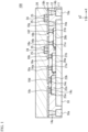
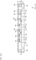
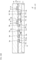
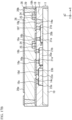
- FIG. 1 is a cross-sectional view of a high-frequency device according to a first embodiment.
- a lead frame 11 includes a metal base 10 and a terminal 10a separated from each other.
- the lead frame 11 is composed of copper as a main component, for example, and is provided with a silver film.
- Chips 20a, 20b and 22a are mounted on the metal base 10.
- the chips 20a and 20b are semiconductor chips, for example, and transistors are formed thereon.
- the chip 22a is, for example, a passive element, in which a capacitor, a line and the like are formed.
- a thickness Ta of the chip 20a is larger than a thickness Tb of the chip 20b.
- Electrodes 21a and 21b are provided on an upper surface of each of the chips 20a and 20b. Electrodes 23a and 23b are provided on an upper surface of the chip 22a.
- the electrodes 21a, 21b, 23a and 23b are metal layers such as a gold layer, for example.
- An insulator layer 12 is provided on the lead frame 11 so as to cover the chips 20a, 20b and 22a.
- the insulator layer 12 is a resin layer such as an epoxy resin.
- a metal layer 18 is provided on the insulator layer 12.
- the metal layer 18 forms wirings 18a to 18h as a rewiring layer.
- the metal layer 18 is, for example, a gold layer or a copper layer.
- a wiring for transmitting a high-frequency signal among the wirings 18a to 18h forms a microstrip line along with the metal base 10.
- the through electrode 14a to 14c and 14e and pillars 16a and 16b are provided through the insulator layer 12.
- the through electrode 14a electrically connects and short-circuits a wiring 18g and the metal base 10.
- the through electrode 14b electrically connects and short-circuits the wiring 18h and the terminal 10a.
- the through electrodes 14c electrically connect and short-circuit wirings 18c and 18d and the electrodes 23a and 23b of the chip 22a, respectively.
- the through electrode 14e electrically connects and short-circuits the wiring 18c and the terminal 10a.
- the through electrodes 14a to 14c and 14e are, for example, a gold layer or a copper layer.
- the pillars 16a electrically connect and short-circuit the wirings 18a and 18b and the electrodes 21a and 21b of the chip 20a, respectively.
- the pillars 16b electrically connect and short-circuit wirings 18e and 18f and the electrodes 21a and 21b of the chip 20b, respectively.
- the pillars 16a and 16b are, for example, a gold layer or a copper layer.
- the width of each of the pillars 16a and 16b is less than the width of each of the through electrodes 14a to 14c and 14e.
- Electronic components 24 are mounted on the insulator layer 12. Each electrode 25 of the electronic components 24 is bonded to the metal layer 18. A solder such as SnAgCu is used for bonding the electrode 25 and the metal layer 18.
- the electronic component 24 is, for example, a discrete component, and includes a chip resistor, a chip capacitor, and a chip inductor.
- An insulator layer 26 is provided on the insulator layer 12 so as to cover the electronic component 24.
- the insulator layer 26 is a resin layer such as an epoxy resin.
- the lead frame 11 has a thickness of, for example, 200 ⁇ m
- the insulator layer 12 has a thickness of, for example, 200 ⁇ m
- the insulator layer 26 has a thickness of, for example, 400 ⁇ m.
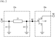
- FIG. 2 is a circuit diagram of the vicinity of the chips 22a and 20a according to the first embodiment.
- a transmission line Z1 is connected between nodes N1 and N2.
- a capacitor C1 is shunt-connected to a node provided on the node N1 side of the transmission line Z 1
- a capacitor C2 is shunt-connected to a node provided on the node N2 side of the transmission line Z1.
- the chip 22a functions as a CLC ⁇ -type circuit.
- a transistor Q1 is provided in the chip 20a.
- the transistor Q1 is, for example, an FET (Field Effect Transistor).
- a source S is grounded, a gate G is connected to the node N2, and a drain D is connected to the node N3.
- the chip 22a functions as a matching circuit for matching an impedance seen from the node N1 to the chip 22a and an impedance seen from the node N2 to the gate G.
- the transistor Q1 amplifies a high-frequency signal input to the node N1 and outputs the amplified high-frequency signal to the drain D.
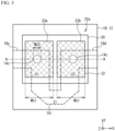
- FIG. 3 is a plan view of the vicinity of the chip 22a according to the first embodiment viewed from an upper side to a lower side along a Z direction.
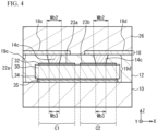
- FIG. 4 is a cross-sectional view taken along line A-A of FIG. 3 .
- the metal layer 32 is illustrated by cross hatching, and each through electrode 14c on a surface where the through electrode 14c is bonded to the metal layer 32 is illustrated by a circle of a dot line.
- the chip 22a is mounted on the metal base 10.
- the chip 22a includes a dielectric substrate 30 and metal layers 32 and 34.
- the metal layer 32 forms the electrodes 23a and 23b.
- the electrodes 23a and 23b are separated from each other on an upper surface of the dielectric substrate 30.
- a metal layer 34 is provided on a lower surface of the dielectric substrate 30.
- the metal layer 34 is provided almost entirely on the lower surface of the dielectric substrate 30.
- the dielectric substrate 30 is, for example, a ceramic substrate.
- the dielectric substrate 30 has a relative dielectric constant of, for example, 5 to 200, which is higher than the relative dielectric constant of the insulator layers 12 and 26.
- a region overlapping the electrode 23a when viewed from the upper side to the lower side along the Z direction constitutes a capacitor C1.
- a region overlapping the electrode 23b as viewed from the upper side to the lower side along the Z direction constitutes a capacitor C2.
- the areas of the electrodes 23a and 23b can be reduced, and the capacitors C1 and C2 can be reduced in size, so that the chip 22a can be reduced in size.
- at least a part of the line 18i forming the transmission line Z1 overlaps the dielectric substrate 30 when viewed from the Z direction, so that the line 18i can be made smaller and the chip 22a can be made smaller.
- the metal layer 34 and the metal base 10 are bonded by a bonding material 35.
- the bonding material 35 is a material obtained by sintering a metal paste such as a silver paste.
- the insulator layer 12 is provided on the metal base 10 so as to cover the chip 22a.
- the through electrodes 14c are provided so as to penetrate through the insulator layer 12.
- the through electrodes 14c are provided on the electrodes 23a and 23b.
- the metal layer 18 is provided on the insulator layer 12.
- the metal layer 18 forms the wirings 18c and 18d and the line 18i.
- the wiring 18c and the line 18i are electrically connected to the electrode 23a via the through electrode 14c.
- the wiring 18d and the line 18i are electrically connected to the electrode 23b via the through electrode 14c.
- the insulator layer 26 is provided on the insulator layer 12 so as to cover the metal layer 18.
- the electrode 23a and the metal layer 34 sandwiching the dielectric substrate 30 form the capacitor C1, and the electrode 23b and the metal layer 34 sandwiching the dielectric substrate 30 form the capacitor C2.
- a reference potential such as a ground potential is supplied to the metal base 10.
- the metal layer 34 has the ground potential.
- the line 18i, the metal layer 34 and the metal base 10 form the transmission line Z1 as the microstrip line.
- the wirings 18c and 18d and the metal base 10 form microstrip lines 19c and 19d, respectively.
- a width Wb1 of each of the electrodes 23a and 23b is, for example, 150 ⁇ m or more.
- the cross-sectional shape of the through electrode 14c is trapezoidal, and widths Wb3 of the through electrodes 14c in contact with the electrodes 23a and 23b are smaller than widths Wb2 of the through electrodes 14c in contact with the wirings 18c and 18d.
- the widths Wb3 are, for example, 100 to 120 ⁇ m, and the widths Wb2 are, for example, 130 to 150 ⁇ m.
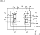
- FIG. 5 is a plan view of the vicinity of the chip 20a according to the first embodiment viewed from the upper side to the lower side along the Z direction.
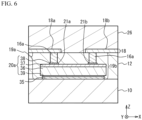
- FIG. 6 is a cross-sectional view taken along line A-A of FIG. 5 .
- a metal layer 38 is illustrated by cross hatching, and each pillar 16a on a surface where the pillar 16a is bonded to the metal layer 38 are illustrated by a circle of a dot line.
- the chip 20a is mounted on the metal base 10.
- a semiconductor layer 37 is provided on a substrate 36.
- the substrate 36 is, for example, a SiC substrate, a sapphire substrate or the like.
- the semiconductor layer 37 includes a GaN channel layer and an AlGaN barrier layer.
- the metal layer 38 is provided on an upper surface of the semiconductor layer 37, and a metal layer 39 is provided on a lower surface of the substrate 36.
- the metal layer 38 forms the electrodes 21a and 21b.
- the electrodes 21a and 21b are, for example, a source electrode and a drain electrode.
- the metal layer 39 is electrically connected to, for example, the source electrode.
- the metal layer 39 is bonded to the metal base 10 via the bonding material 35.
- the bonding material 35 is, for example, a sintered metal paste.
- the insulator layer 12 is provided so as to cover the chip 20a.
- the metal layer 18 is provided on an upper surface of the insulator layer 12.
- the metal layer 18 forms the wirings 18a and 18b.
- the wirings 18a and 18b and the metal base 10 form microstrip lines 19a and 19b, respectively.
- the insulator layer 26 is provided on the insulator layer 12 so as to cover the metal layer 18.
- the wirings 18a and 18b are electrically connected to the electrodes 21a and 21b via the pillars 16a, respectively.
- the pillars 16a may be formed on the electrodes 21a and 21b by a plating method.
- the pillars 16a may be formed on the electrodes 21a and 21b by using a stud bump method.
- Widths Wa1 of the electrodes 21a and 21b are, for example, 100 ⁇ m
- widths Wa2 of the pillars 16a are, for example, 70 ⁇ m.
- the microstrip lines 19a to 19d can be formed by the wirings 18a to 18d connected to the chips 20a and 22a, the high-frequency characteristics can be improved compared with the use of the bonding wires as described in Patent Document 1.
- FIGs. 7A to 10B are cross-sectional views illustrating a method of manufacturing the high-frequency device according to the first embodiment.
- the lead frame 11 is prepared.
- the size of the lead frame 11 is, for example, 500 mm x 500 mm.
- the chips 20a, 20b and 22a are mounted on the metal base 10.
- the pillars 16a and 16b are provided on the electrodes 21a and 21b of the chips 20a and 20b.
- No pillar is provided on the electrodes 23a and 23b of the chip 22a.
- a bonding material which is a metal paste such as, for example, nano-silver paste is partially coated on the metal base 10.
- the chips 20a, 20b and 22a are mounted on the bonding material and subjected to heat treatment.
- the bonding material is sintered by heat treatment.
- the chips 20a, 20b and 22a are mounted on the metal base 10. Since the chip 20a is thicker than 20b, the upper surfaces of the pillars 16a are positioned on the +Z side along the Z direction from the upper surface of the pillar 16b.
- the insulator layer 12 is formed on the lead frame 11 so as to cover the chips 20a, 20b and 22a.
- a resin film is adhered to the lead frame 11 by using a vacuum laminator, and the insulation layer 12 is cured by heat treatment.
- the insulator layer 12 is formed.
- the insulator layer 12 may be formed by applying a softened resin on the lead frame 11 and curing the resin by heat treatment, as in the case of molding.
- the insulator layer 12 is formed so as to cover the pillars 16a and 16b.
- the upper surface of the insulator layer 12 is polished or ground.
- the upper surfaces of the pillars 16a and 16b are exposed from the upper surface of the insulator layer 12.
- the upper surfaces of the insulator layer 12 and the pillars 16a and 16b are substantially flush with each other.
- through holes 15a to 15c and 15e penetrating through the insulator layer 12 are formed.
- the through holes 15a to 15c and 15e are formed by irradiating the insulating layer 12 with laser beams 13a to 13c and 13e, respectively.
- the laser beams 13a to 13c and 13e for example, ultraviolet light, visible light or infrared light.
- an ultraviolet laser device or a carbon dioxide laser device using a harmonic of a YAG (Yittrium Aluminum Garnet) laser is used as the laser device.
- the through holes 15a, 15b and 15e reaching the upper surface of the lead frame 11 are formed, the power of the laser beams 13a, 13b and 13e is increased.
- the through hole 15c reaching the upper surface of the chip 22a is formed, the power of the laser beam 13c is reduced.
- the through electrodes 14a to 14c and 14e are formed in the through holes 15a to 15c and 15e, respectively.
- the through electrodes 14a to 14c and 14e are formed by, for example, a plating method.
- a plating method for example, a seed layer is formed by using an electroless plating method, and a plating layer is formed on the seed layer by using an electrolytic plating method.
- the metal layer 18 is formed on the insulator layer 12.
- the metal layer 18 is formed by, for example, the plating method. Desired region of the metal layer 18 are removed by, for example, an etching method.
- the wirings 18a to 18h are formed by the metal layer 18.
- a metal film (for example, a gold film) for improving solder wettability may be formed on the surface of the metal layer 18.
- the electronic components 24 are mounted on the metal layer 18 using the bonding material.
- the bonding material bonds the electrodes 25 of the electronic components 24 and the metal layer 18.
- the insulator layer 26 is formed on the insulator layer 12 so as to cover the metal layer 18 and the electronic components 24.
- the insulator layer 26 is formed by, for example, a molding method or a lamination method.
- the lead frame 11 and the insulator layers 12 and 26 are cut into individual pieces. For the cutting, for example, a dicing method using a dicing blade is used.
- the high-frequency device according to the first embodiment is completed.
- FIG. 11 is a block diagram illustrating an example of the amplifying apparatus according to the first embodiment.
- an amplifier 102 includes transistors Q1 to Q3.
- the transistors Q1 to Q3 are FETs, for example.
- the transistor Q1 is a driver amplifier, and the transistors Q2 and Q3 are a main amplifier and a peak amplifier of a Dockerty amplifier, respectively.
- An input terminal Tin is connected to a gate G1 of the transistor Q1 via a matching circuit 60.
- the matching circuit 60 matches an impedance seen from the input terminal Tin to the matching circuit 60 with an impedance seen from the matching circuit 60 to the gate G1.
- a gate bias voltage is applied to the gate G1 from a bias terminal Tg1.
- a source S1 of the transistor Q1 is grounded.
- a drain D1 of the transistor Q1 is connected to a distributor 66 via a matching circuit 61.
- the matching circuit 61 matches an impedance seen from the drain D1 to the matching circuit 61 with an impedance seen from the matching circuit 61 to the distributor 66.
- a drain bias voltage is applied to the drain D1 from a bias terminal Td1.
- the distributor 66 distributes the high-frequency signal output from the matching circuit 61 into two paths.
- the distributor 66 is connected to a gate G2 of the transistor Q2 via a phase shifter 68 and a matching circuit 62.
- the phase shifter 68 shifts the phase of the high-frequency signal output from the distributor 66.
- the matching circuit 62 matches an impedance seen from the distributor 66 to the matching circuit 62 with an impedance seen from the matching circuit 62 to the gate G2.
- a gate bias voltage is applied to the gate G2 from a bias terminal Tg2.
- a source S2 of the transistor Q2 is grounded.
- a drain D2 of the transistor Q2 is connected to a combiner 67 via a matching circuit 64.
- the matching circuit 64 matches an impedance seen from the drain D2 to the matching circuit 64 with an impedance seen from the matching circuit 64 to the combiner 67.
- a drain bias voltage is applied to the drain D2 from a bias terminal Td2.
- the distributor 66 is connected to a gate G3 of the transistor Q3 via a phase shifter 69 and a matching circuit 63.
- the phase shifter 69 shifts the phase of the high-frequency signal output from the distributor 66.
- the matching circuit 63 matches an impedance seen from the distributor 66 to the matching circuit 63 with an impedance seen from the matching circuit 63 to the gate G3.
- a gate bias voltage is applied to the gate G3 from a bias terminal Tg3.
- a source S3 of the transistor Q3 is grounded.
- a drain D3 of the transistor Q3 is connected to the combiner 67 via a matching circuit 65.
- the matching circuit 65 matches an impedance seen from the drain D3 to the matching circuit 65 with an impedance seen from the matching circuit 65 to the combiner 67.
- a drain bias voltage is applied to the drain D3 from a bias terminal Td3.
- the combiner 67 combines the high-frequency signal output from the drain D2 and the high-frequency signal output from the drain D3 and outputs the combined high-frequency signal to the output terminal Tout.
- Bias circuits are provided between the bias terminals Tg1 to Tg3 and Td1 to Td3 and the transistors Q1 to Q3, but their illustration is omitted.
- the high-frequency signal input from the input terminal Tin is amplified by the transistor Q1.
- the transistors Q2 and Q3, the distributor 66 and the combiner 67 form a Jardinerty amplifier.
- the distributor 66 distributes the amplified high-frequency signal to a plurality of high-frequency signals and outputs them to the transistors Q2 and Q3.
- the transistor Q2 is a main amplifier and amplifies one of the high-frequency signals distributed by the distributor 66.
- the transistor Q3 is a peak amplifier and amplifies the other of the high-frequency signals distributed by the distributor 66.
- the combiner 67 combines the high-frequency signal amplified by the transistor Q2 and the high-frequency signal amplified by the transistor Q3, and outputs the combined high-frequency signal to the output terminal Tout.
- the high-frequency signal input to the input terminal Tin and output from the output terminal Tout is, for example, a signal of 0.5 GHz to 100 GHz, and typically a signal of 0.5 GHz to 10 GHz.
- the transistor Q2 performs class A or class B operation, and transistor Q3 performs class C operation.
- the transistor Q2 mainly amplifies the input signal.
- the peak of the input signal is amplified by the transistor Q3 in addition to the transistor Q2.
- the transistors Q2 and Q3 amplify the input signal.
- the impedance seen from the transistor Q2 to the combiner 67 is twice a load R of the output terminal Tout (for example, 2 ⁇ 50 ⁇ ).
- each of the impedance seen from the transistor Q2 to the combiner 67 and the impedance seen from the transistor Q3 to the combiner 67 is the load R (for example, 50 ⁇ ).
- the matching circuits 62 and 64 are adjusted so that the transistor Q2 operates optimally at the saturated output in the load 2R when the transistor Q3 does not operate, while the matching circuits 62 and 64 are adjusted so that the transistor Q2 operates optimally at the saturated output in the load R when the transistor Q3 operates.
- the matching circuits 63 and 65 are adjusted so that the impedance viewed from the combiner 67 to the transistor Q3 opens when the transistor Q3 does not operate, while the matching circuits 63 and 65 are adjusted so that the transistor Q3 operates optimally at the saturated output in the load R when the transistor Q3 operates.
- At least one of transistors Q1 to Q3 may be provided on the chip 20a or 20b with the pillars 16a or 16b, and at least one of the matching circuits 60 to 65 may be provided on chip 22a with no pillars.
- the input terminal Tin, the output terminal Tout, and the bias terminals Tg1 to Tg3 and Td1 to Td3 can be the terminal 10a.
- the chips 20a and 20b are connected to the metal layer 18 by using the through electrodes 14c instead of using the pillars 16a and 16b.
- the through holes 15c are formed using the laser beam 13c as illustrated in FIG. 9A
- the widths Wb3 (see FIG. 4 ) of the through electrode 14c are made smaller than the widths Wa1 (see FIG. 5 ) of the electrodes 21a and 21b of the chips 20a and 20b.
- the widths Wa1 are 100 ⁇ m
- the widths Wb3 are set to 80 ⁇ m in consideration of the margin. It is difficult to make the widths Wb3 100 ⁇ m or less using a laser beam.
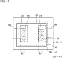
- FIG. 12 is a plan view of the vicinity of the chip 20a according to the first comparative example.
- a target mounting position 40 which is a target position for mounting the chip 20a on the metal base 10
- the alignment accuracy for mounting the chip 20a on the metal base 10 is 15 to 25 ⁇ m. Therefore, the mounting position of the chip 20a may be shifted from the target mounting position 40.
- the through electrode 14c protrudes from the electrodes 21a and 21b. It is conceivable to widen the widths Wa1 of the electrodes 21a and 21b.
- the cost per unit area of the chips 20a and 20b is high (for example, the cost per unit area of the GaN HEMT is high), the cost is increased by increasing the widths Wa1.
- FIG. 13 is a plan view of the vicinity of the chip 20a according to the first embodiment.
- the chip 20a is provided with the pillars 16a. Since the pillars 16a are formed by using a semiconductor manufacturing process, the alignment accuracy between the pillars 16a and the electrodes 21a and 21b is 10 ⁇ m or less, and the pillars 16a hardly deviate from the electrodes 21a and 21b. Therefore, even when the mounting position of the chip 20a deviates from the target mounting position 40, the pillars 16a do not detach from the electrodes 21a and 21b. If the wirings 18a and 18b are formed large, the pillars 16a do not detach from the wirings 18a and 18b. Therefore, the electrodes 21a and 21b of the semiconductor chip 20a need not be increased in size, and the cost of the semiconductor chip 20a can be suppressed.
- the chip 20a (first chip) having the pillars 16a (first pillar) provided on its upper surface is mounted on the metal base 10.
- the insulator layer 12 covering the semiconductor chip 20a is formed on the metal base 10.
- the upper surfaces of the pillars 16a are exposed from the insulator layer 12.
- Wirings 18a and 18b (first wiring) which are connected to the pillars 16a and transmit the high-frequency signals are formed on the insulator layer 12.
- the pillars 16a can be prevented from being detached from the electrodes 21a and 21b. Therefore, it is not necessary to increase the size of the chip 20a, and the manufacturing cost of the high-frequency device can be suppressed.
- the chip 20a has been described as the semiconductor chip, the chip 20a may be other than the semiconductor chip if the cost of providing the pillars 16a is less than the cost of increasing the size of the chip 20a.
- the chip 22a (second chip) is mounted on the metal base 10.
- the insulator layer 12 covering the chips 20a and 22a is formed.
- the through holes 15c (first through hole) reaching the upper surface of the chip 22a are formed in the insulator layer 12.
- the through electrodes 14c (first through electrode) connected to the upper surface of the chip 22a are formed in the through holes 15c.
- the wirings 18c and 18d (second wiring) connected to the through electrodes 14c are formed on the insulator layer 12.
- the manufacturing cost can be reduced by increasing the size of the electrodes 23a and 23b rather than providing the pillars.
- the areas of the electrodes 23a and 23b are large, forming the pillars on the chip 22a increases the manufacturing cost of the chip 22a. In these cases, it is preferable to provide the through electrodes 14c without providing the pillars on the chip 22a.
- the chip 22a is a passive element having the dielectric substrate 30 and the electrodes 23a and 23b provided on the upper surface of the dielectric substrate 30.
- the areas of the electrodes 23a and 23b are large.
- the manufacturing cost per unit area of the passive element is lower than that of the semiconductor chip. Therefore, it is preferable that the through electrodes 14c are provided on the chip 22a without providing the pillars.
- the chip 20a includes the transistor Q1. Since the chip 20a in which the transistor Q1 is formed has a high manufacturing cost per unit area, the areas of the electrodes 21a and 21b are small. Therefore, it is preferable to provide the pillars 16a on the chip 20a.
- the passive element provided on the chip 22a is at least a part of the matching circuit connected to the transistor Q1 provided on the chip 20a.
- the cost of the high-frequency device including the transistor Q1 and the matching circuit can be reduced.
- the chip 20a includes the electrodes 21a and 21b (first electrodes) to which the pillars 16a are bonded.
- the chip 22a includes the electrodes 23a and 23b (second electrode) to which the through electrodes 14c are bonded.
- the widths Wb 1 of the electrodes 23a and 23b are larger than the widths Wa1 of the electrodes 21a and 21b. Since the minimum widths Wa1 of the electrodes 21a and 21b can be reduced, the manufacturing cost of the chip 20a can be suppressed. Since no pillar is provided for the chip 22a having large minimum widths Wb1 of the electrodes 23a and 23b, the manufacturing cost of the chip 22a can be suppressed.
- the through holes 15c are formed by irradiating the insulating layer 12 with the laser beam 13c.
- the through holes 15c become large. Therefore, it is preferable to provide the through electrodes 14c on the chip 22a provided with the electrodes 23a and 23b having large widths.
- the chip 20b (third chip) having the pillars 16b (second pillar) provided on its upper surface is mounted on the metal base 10.
- the insulator layer 12 covering the chips 20a and 20b is formed.
- the upper surfaces of the pillars 16a and 16b are exposed from the upper surface of the insulator layer 12 by polishing or grinding the insulator layer 12 covering the pillars 16a and 16b.
- the wirings 18e and 18f (third wiring) connected to the pillars 16b are formed on the insulator layer 12.
- the metal layer 18 can be brought into contact with the pillars 16a and 16b even when the heights (positions in the Z direction) of the upper surfaces of the pillars 16a and 16b are different from each other as illustrated in FIG. 7B .
- the heights of the upper surfaces of the pillars 16a and 16b are different, an example in which the thicknesses Ta and Tb of the chips 20a and 20b are different has been described.
- the pillars 16a and 16b may have different heights due to differences in manufacturing processes or manufacturing errors.
- the through hole 15a (second through hole) reaching the upper surface of the metal base 10 is formed in the insulator layer 12.
- the through electrode 14a (second through electrode) connected to the upper surface of the metal base 10 is formed in the through hole 15a.
- the wiring 18g (fourth wiring) connected to the through electrode 14a is formed on the insulator layer 12.
- the wiring 18g connected to the metal base 10 and supplied with the ground potential can be provided on the insulator layer 12.
- the electronic components 24 are mounted on the metal layer 18 provided on the insulator layer 12.
- the electronic components 24 can be mounted without increasing the size of the high-frequency device.
- FIGs. 14A to 15B are cross-sectional views illustrating a method of manufacturing a high-frequency device according to a first modification of the first embodiment.
- the through holes 15a to 15c and 15e are formed without polishing the upper surface of the insulator layer 12 as illustrated in FIG. 8B of the first embodiment, the through holes 15d that expose the upper surfaces of the pillars 16a and 16b are formed using a laser beam 13d. The through holes 15d do not reach the upper surfaces of the chips 20a and 20b.
- the metal layer 18 when the metal layer 18 is formed, a part of the metal layer 18 is formed so as to be connected to the through electrodes 14d.
- the wirings 18a, 18b, 18e and 18f connected to the chips 20a and 20b via the through electrodes 14d and the pillars 16a and 16b can be formed.
- the high-frequency device according to the first modification of the first embodiment can be manufactured.
- Other steps are the same as those in the first embodiment, and description thereof is omitted.
- the upper surfaces of the pillars 16a and 16b may be exposed from the insulator layer 12 through the through holes 15d as illustrated in FIG. 14A .
- the pillars 16a and 16b may be connected to the metal layer 18 via the through electrodes 14d.
- the pillars 16a and 16b can be electrically connected to the metal layer 18 even if the mounting position of the chips 20a and 20b deviates from the target mounting position 40.
- FIGs. 16A to 16B are cross-sectional views illustrating a method of manufacturing a high-frequency device according to a second modification of the first embodiment.
- the terminals 10a and the through electrodes 14b and 14e as illustrated in FIG. 9B of the first embodiment are not provided.
- the metal layer 18 is formed, the electronic components 24 are mounted thereon, and the insulator layer 26 is formed.
- through electrodes 29 are formed through the insulator layer 26 and connected to the metal layer 18.
- the through electrodes 29 are formed by forming through holes penetrating through the insulator layer 26 and reaching the upper surface of the metal layer 18, and forming the through electrodes 29 in the through holes, similarly to the through electrodes 14b and 14e of the first embodiment.
- a metal layer 28 is formed on the insulator layer 26.
- the metal layer 28 forms a shield layer 28a and terminals 28b.
- the terminals 28b may be provided on the upper surface of the insulator layer 26.
- the shield layer 28a may be provided on the upper surface of the insulator layer 26.
- an amplifying apparatus has been described as an example of the high-frequency apparatus, but the high-frequency apparatus may be other than the amplifying apparatus.
- the High-frequency device may be provided with one or a plurality of passive elements, or with one or a plurality of semiconductor chips.
Landscapes
- Engineering & Computer Science (AREA)
- Power Engineering (AREA)
- Microelectronics & Electronic Packaging (AREA)
- Semiconductor Integrated Circuits (AREA)
- Amplifiers (AREA)
Abstract
Description
- The present disclosure relates to a method of manufacturing a high-frequency device.
- There is known a semiconductor device in which a semiconductor chip is mounted face-up on a metal base in a package including the metal base and an insulating frame provided on the metal base, and the semiconductor chip is electrically connected to a pattern on the insulating frame using a bonding wire (for example, Patent Document 1:
Japanese Patent Application Laid-Open No. 2019-176149 Japanese Patent Application Laid-Open No. 2001-196865 - A method of manufacturing a high-frequency device according to the present disclosure includes: mounting a first chip having a first pillar on an upper surface thereof on a metal base; forming an insulator layer covering the first chip on the metal base; exposing an upper surface of the first pillar from the insulator layer; and forming a first wiring connected to the first pillar on the insulator layer and transmitting a high-frequency signal.
-
-
FIG. 1 is a cross-sectional view of a high-frequency device according to a first embodiment. -
FIG. 2 is a circuit diagram of the vicinity ofchips -
FIG. 3 is a plan view of the vicinity of thechip 22a according to the first embodiment. -
FIG. 4 is a cross-sectional view taken along line A-A ofFIG. 3 . -
FIG. 5 is a plan view of the vicinity of thechip 20a according to the first embodiment. -
FIG. 6 is a cross-sectional view taken along line A-A ofFIG. 5 . -
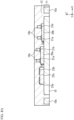
FIG. 7A is a cross-sectional view illustrating a method of manufacturing the high-frequency device according to the first embodiment. -
FIG. 7B is a cross-sectional view illustrating a method of manufacturing the high-frequency device according to the first embodiment. -
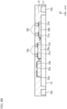
FIG. 8A is a cross-sectional view illustrating a method of manufacturing the high-frequency device according to the first embodiment. -
FIG. 8B is a cross-sectional view illustrating a method of manufacturing the high-frequency device according to the first embodiment. -
FIG. 9A is a cross-sectional view illustrating a method of manufacturing the high-frequency device according to the first embodiment. -
FIG. 9B is a cross-sectional view illustrating a method of manufacturing the high-frequency device according to the first embodiment. -
FIG. 10A is a cross-sectional view illustrating a method of manufacturing the high-frequency device according to the first embodiment. -
FIG. 10B is a cross-sectional view illustrating a method of manufacturing the high-frequency device according to the first embodiment. -
FIG. 11 is a block diagram illustrating an example of an amplifying apparatus according to the first embodiment. -
FIG. 12 is a plan view of the vicinity of thechip 20a according to a first comparative example. -
FIG. 13 is a plan view of the vicinity of thechip 20a according to the first embodiment. -
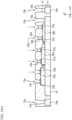
FIG. 14A is a cross-sectional view illustrating a method of manufacturing a high-frequency device according to a first modification of the first embodiment. -
FIG. 14B is a cross-sectional view illustrating a method of manufacturing the high-frequency device according to the first modification of the first embodiment. -
FIG. 15A is a cross-sectional view illustrating a method of manufacturing the high-frequency device according to a first modification of the first embodiment. -
FIG. 15B is a cross-sectional view illustrating a method of manufacturing the high-frequency device according to the first modification of the first embodiment. -
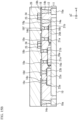
FIG. 16A is a cross-sectional view illustrating a method of manufacturing a high-frequency device according to a second modification of the first embodiment. -
FIG. 16B is a cross-sectional view illustrating a method of manufacturing the high-frequency device according to the second modification of the first embodiment. -
FIG. 17A is a cross-sectional view illustrating a method of manufacturing the high-frequency device according to the second modification of the first embodiment. -
FIG. 17B is a cross-sectional view illustrating a method of manufacturing the high-frequency device according to the second modification of the first embodiment. - In
Patent Document 1, high-frequency characteristics are deteriorated because a high-frequency signal is transmitted through the bonding wire. It is considered that a microstrip line is used as a transmission line. However, when the alignment accuracy between the chip and the line is poor, the sizes of electrodes on the chip are increased and the cost of the chip is increased. - The present disclosure has been made in view of the above problems, and an object of the present disclosure is to provide a method of manufacturing a high-frequency device capable of reducing costs.
- First, the contents of the embodiments of this disclosure are listed and explained.
- (1) A method of manufacturing a high-frequency device according to the present disclosure includes: mounting a first chip having a first pillar on an upper surface thereof on a metal base; forming an insulator layer covering the first chip on the metal base; exposing an upper surface of the first pillar from the insulator layer; and forming a first wiring connected to the first pillar on the insulator layer and transmitting a high-frequency signal. Thus, it is possible to provide the method for manufacturing the high-frequency device capable of reducing the cost.
- (2) The method of manufacturing the high-frequency device may further include: mounting a second chip on the metal base; forming a first through hole reaching an upper surface of the second chip in the insulator layer; forming a first through electrode connected to an upper surface of the second chip in the first through hole; and forming a second wiring connected to the first through electrode on the insulator layer. The forming the insulator layer may include forming the insulator layer covering the first chip and the second chip. Thereby, it is possible to suppress the cost.
- (3) The second chip may be a passive element including a dielectric substrate and an electrode provided on an upper surface of the dielectric substrate. Thereby, it is possible to suppress the cost.
- (4) The first chip may include a transistor. Thereby, it is possible to suppress the cost.
- (5) The passive element may be at least a part of a matching circuit connected to the transistor. Thereby, it is possible to suppress the cost of the high-frequency device having the matching circuit.
- (6) The first chip may include a first electrode to which the first pillar is bonded, the second chip may include a second electrode to which the first through electrode is bonded, and a width of the second electrode may be larger than that of the first electrode. Thereby, it is possible to suppress the cost.
- (7) The forming the first through hole may include forming the first through hole by irradiating the insulating layer with a laser beam. Thereby, the first through electrode can be provided on the second chip having a wider second electrode.
- (8) The method of manufacturing the high-frequency device may further include: mounting a third chip having a second pillar on an upper surface thereof on the metal base; and forming a third wiring connected to the second pillar on the insulator layer. The forming the insulator layer may include forming the insulator layer covering the first chip and the third chip, and the exposing the upper surface of the first pillar from the insulator layer may include exposing the upper surfaces of the first pillar and the second pillar from the upper surface of the insulator layer by polishing or grinding the insulator layer covering the first pillar and the second pillar. Thereby, the first pillar can be connected to the first wiring and the second pillar can be in contact with the third wiring even if the heights of the first and second pillars are different from each other.
- (9) The method of manufacturing the high-frequency device may further include: forming a second through hole reaching an upper surface of the metal base in the insulator layer; forming a second through electrode connected to the upper surface of the metal base in the second through hole; and forming a fourth wiring connected to the second through electrode on the insulator layer. Thereby, the fourth wiring connected to the metal base can be formed on the metal base.
- (10) The method of manufacturing the high-frequency device may further include mounting an electronic component on a metal layer provided on the insulator layer. Therefore, the high-frequency device can be reduced in size.
- Specific examples of a high frequency circuit in accordance with embodiments of the present disclosure are described below with reference to the drawings. The present disclosure is not limited to these examples, but is indicated by the claims, which are intended to include all modifications within the meaning and scope of the claims.
-
FIG. 1 is a cross-sectional view of a high-frequency device according to a first embodiment. As illustrated inFIG. 1 , in a high-frequency device 100, alead frame 11 includes ametal base 10 and a terminal 10a separated from each other. Thelead frame 11 is composed of copper as a main component, for example, and is provided with a silver film.Chips metal base 10. Thechips chip 22a is, for example, a passive element, in which a capacitor, a line and the like are formed. A thickness Ta of thechip 20a is larger than a thickness Tb of thechip 20b.Electrodes chips Electrodes chip 22a. Theelectrodes insulator layer 12 is provided on thelead frame 11 so as to cover thechips insulator layer 12 is a resin layer such as an epoxy resin. Ametal layer 18 is provided on theinsulator layer 12. Themetal layer 18 forms wirings 18a to 18h as a rewiring layer. Themetal layer 18 is, for example, a gold layer or a copper layer. A wiring for transmitting a high-frequency signal among thewirings 18a to 18h forms a microstrip line along with themetal base 10. - Through
electrodes 14a to 14c and 14e andpillars insulator layer 12. The throughelectrode 14a electrically connects and short-circuits awiring 18g and themetal base 10. The throughelectrode 14b electrically connects and short-circuits thewiring 18h and the terminal 10a. The throughelectrodes 14c electrically connect and short-circuit wirings electrodes chip 22a, respectively. The throughelectrode 14e electrically connects and short-circuits thewiring 18c and the terminal 10a. The throughelectrodes 14a to 14c and 14e are, for example, a gold layer or a copper layer. Thepillars 16a electrically connect and short-circuit thewirings electrodes chip 20a, respectively. Thepillars 16b electrically connect and short-circuit wirings electrodes chip 20b, respectively. Thepillars pillars electrodes 14a to 14c and 14e. -
Electronic components 24 are mounted on theinsulator layer 12. Eachelectrode 25 of theelectronic components 24 is bonded to themetal layer 18. A solder such as SnAgCu is used for bonding theelectrode 25 and themetal layer 18. Theelectronic component 24 is, for example, a discrete component, and includes a chip resistor, a chip capacitor, and a chip inductor. Aninsulator layer 26 is provided on theinsulator layer 12 so as to cover theelectronic component 24. Theinsulator layer 26 is a resin layer such as an epoxy resin. Thelead frame 11 has a thickness of, for example, 200 µm, theinsulator layer 12 has a thickness of, for example, 200 µm, and theinsulator layer 26 has a thickness of, for example, 400 µm. -
FIG. 2 is a circuit diagram of the vicinity of thechips FIG. 2 , in thechip 22a, a transmission line Z1 is connected between nodes N1 and N2. A capacitor C1 is shunt-connected to a node provided on the node N1 side of thetransmission line Z 1, and a capacitor C2 is shunt-connected to a node provided on the node N2 side of the transmission line Z1. Thechip 22a functions as a CLC π-type circuit. A transistor Q1 is provided in thechip 20a. The transistor Q1 is, for example, an FET (Field Effect Transistor). A source S is grounded, a gate G is connected to the node N2, and a drain D is connected to the node N3. Thechip 22a functions as a matching circuit for matching an impedance seen from the node N1 to thechip 22a and an impedance seen from the node N2 to the gate G. The transistor Q1 amplifies a high-frequency signal input to the node N1 and outputs the amplified high-frequency signal to the drain D. -
FIG. 3 is a plan view of the vicinity of thechip 22a according to the first embodiment viewed from an upper side to a lower side along a Z direction.FIG. 4 is a cross-sectional view taken along line A-A ofFIG. 3 . InFIG. 3 , themetal layer 32 is illustrated by cross hatching, and each throughelectrode 14c on a surface where the throughelectrode 14c is bonded to themetal layer 32 is illustrated by a circle of a dot line. As illustrated inFIGs. 3 and4 , thechip 22a is mounted on themetal base 10. Thechip 22a includes adielectric substrate 30 andmetal layers metal layer 32 forms theelectrodes electrodes dielectric substrate 30. Ametal layer 34 is provided on a lower surface of thedielectric substrate 30. Themetal layer 34 is provided almost entirely on the lower surface of thedielectric substrate 30. Thedielectric substrate 30 is, for example, a ceramic substrate. Thedielectric substrate 30 has a relative dielectric constant of, for example, 5 to 200, which is higher than the relative dielectric constant of the insulator layers 12 and 26. Among a laminated body 20c composed of themetal layer 34, thedielectric substrate 30 and themetal layer 32, a region overlapping theelectrode 23a when viewed from the upper side to the lower side along the Z direction constitutes a capacitor C1. A region overlapping theelectrode 23b as viewed from the upper side to the lower side along the Z direction constitutes a capacitor C2. By increasing a dielectric constant of thedielectric substrate 30, the areas of theelectrodes chip 22a can be reduced in size. In addition, at least a part of theline 18i forming the transmission line Z1 overlaps thedielectric substrate 30 when viewed from the Z direction, so that theline 18i can be made smaller and thechip 22a can be made smaller. Themetal layer 34 and themetal base 10 are bonded by abonding material 35. Thebonding material 35 is a material obtained by sintering a metal paste such as a silver paste. - The
insulator layer 12 is provided on themetal base 10 so as to cover thechip 22a. The throughelectrodes 14c are provided so as to penetrate through theinsulator layer 12. The throughelectrodes 14c are provided on theelectrodes metal layer 18 is provided on theinsulator layer 12. Themetal layer 18 forms thewirings line 18i. Thewiring 18c and theline 18i are electrically connected to theelectrode 23a via the throughelectrode 14c. Thewiring 18d and theline 18i are electrically connected to theelectrode 23b via the throughelectrode 14c. Theinsulator layer 26 is provided on theinsulator layer 12 so as to cover themetal layer 18. - The
electrode 23a and themetal layer 34 sandwiching thedielectric substrate 30 form the capacitor C1, and theelectrode 23b and themetal layer 34 sandwiching thedielectric substrate 30 form the capacitor C2. A reference potential such as a ground potential is supplied to themetal base 10. As a result, themetal layer 34 has the ground potential. Theline 18i, themetal layer 34 and themetal base 10 form the transmission line Z1 as the microstrip line. The wirings 18c and 18d and themetal base 10form microstrip lines electrodes electrode 14c is trapezoidal, and widths Wb3 of the throughelectrodes 14c in contact with theelectrodes electrodes 14c in contact with thewirings -
FIG. 5 is a plan view of the vicinity of thechip 20a according to the first embodiment viewed from the upper side to the lower side along the Z direction.FIG. 6 is a cross-sectional view taken along line A-A ofFIG. 5 . InFIG. 5 , ametal layer 38 is illustrated by cross hatching, and eachpillar 16a on a surface where thepillar 16a is bonded to themetal layer 38 are illustrated by a circle of a dot line. As illustrated inFIGs. 5 and6 , thechip 20a is mounted on themetal base 10. In thechip 20a, asemiconductor layer 37 is provided on asubstrate 36. When the transistor provided in thechip 20a is a GaN HEMT (Gallium Nitride High Electron Mobility Transistor), thesubstrate 36 is, for example, a SiC substrate, a sapphire substrate or the like. Thesemiconductor layer 37 includes a GaN channel layer and an AlGaN barrier layer. Themetal layer 38 is provided on an upper surface of thesemiconductor layer 37, and ametal layer 39 is provided on a lower surface of thesubstrate 36. Themetal layer 38 forms theelectrodes electrodes metal layer 39 is electrically connected to, for example, the source electrode. Themetal layer 39 is bonded to themetal base 10 via thebonding material 35. Thebonding material 35 is, for example, a sintered metal paste. - The
insulator layer 12 is provided so as to cover thechip 20a. Themetal layer 18 is provided on an upper surface of theinsulator layer 12. Themetal layer 18 forms thewirings wirings metal base 10form microstrip lines insulator layer 26 is provided on theinsulator layer 12 so as to cover themetal layer 18. Thewirings electrodes pillars 16a, respectively. Thepillars 16a may be formed on theelectrodes pillars 16a may be formed on theelectrodes electrodes pillars 16a are, for example, 70 µm. - As illustrated in
FIGs. 3 to 6 , since themicrostrip lines 19a to 19d can be formed by thewirings 18a to 18d connected to thechips Patent Document 1. -
FIGs. 7A to 10B are cross-sectional views illustrating a method of manufacturing the high-frequency device according to the first embodiment. As illustrated inFIG. 7A , thelead frame 11 is prepared. The size of thelead frame 11 is, for example, 500 mm x 500 mm. As illustrated inFIG. 7B , thechips metal base 10. Thepillars electrodes chips electrodes chip 22a. A bonding material which is a metal paste such as, for example, nano-silver paste is partially coated on themetal base 10. Thereafter, thechips chips metal base 10. Since thechip 20a is thicker than 20b, the upper surfaces of thepillars 16a are positioned on the +Z side along the Z direction from the upper surface of thepillar 16b. - As illustrated in
FIG. 8A , theinsulator layer 12 is formed on thelead frame 11 so as to cover thechips lead frame 11 by using a vacuum laminator, and theinsulation layer 12 is cured by heat treatment. Thus, theinsulator layer 12 is formed. Theinsulator layer 12 may be formed by applying a softened resin on thelead frame 11 and curing the resin by heat treatment, as in the case of molding. Theinsulator layer 12 is formed so as to cover thepillars - As illustrated in
FIG. 8B , the upper surface of theinsulator layer 12 is polished or ground. Thus, the upper surfaces of thepillars insulator layer 12. The upper surfaces of theinsulator layer 12 and thepillars - As illustrated in
FIG. 9A , throughholes 15a to 15c and 15e penetrating through theinsulator layer 12 are formed. The throughholes 15a to 15c and 15e are formed by irradiating the insulatinglayer 12 withlaser beams 13a to 13c and 13e, respectively. Thelaser beams 13a to 13c and 13e, for example, ultraviolet light, visible light or infrared light. For example, an ultraviolet laser device or a carbon dioxide laser device using a harmonic of a YAG (Yittrium Aluminum Garnet) laser is used as the laser device. When the throughholes lead frame 11 are formed, the power of thelaser beams hole 15c reaching the upper surface of thechip 22a is formed, the power of thelaser beam 13c is reduced. - As illustrated in
FIG. 9B , the throughelectrodes 14a to 14c and 14e are formed in the throughholes 15a to 15c and 15e, respectively. The throughelectrodes 14a to 14c and 14e are formed by, for example, a plating method. As the plating method, for example, a seed layer is formed by using an electroless plating method, and a plating layer is formed on the seed layer by using an electrolytic plating method. - As illustrated in
FIG. 10A , themetal layer 18 is formed on theinsulator layer 12. Themetal layer 18 is formed by, for example, the plating method. Desired region of themetal layer 18 are removed by, for example, an etching method. Thewirings 18a to 18h are formed by themetal layer 18. A metal film (for example, a gold film) for improving solder wettability may be formed on the surface of themetal layer 18. - As illustrated in
FIG. 10B , theelectronic components 24 are mounted on themetal layer 18 using the bonding material. The bonding material bonds theelectrodes 25 of theelectronic components 24 and themetal layer 18. Thereafter, theinsulator layer 26 is formed on theinsulator layer 12 so as to cover themetal layer 18 and theelectronic components 24. Theinsulator layer 26 is formed by, for example, a molding method or a lamination method. Thelead frame 11 and the insulator layers 12 and 26 are cut into individual pieces. For the cutting, for example, a dicing method using a dicing blade is used. Thus, the high-frequency device according to the first embodiment is completed. - A high-frequency power amplifying apparatus used in a base station for mobile communication will be described as an example of the high-frequency device.
FIG. 11 is a block diagram illustrating an example of the amplifying apparatus according to the first embodiment. As illustrated inFIG. 11 , anamplifier 102 includes transistors Q1 to Q3. The transistors Q1 to Q3 are FETs, for example. The transistor Q1 is a driver amplifier, and the transistors Q2 and Q3 are a main amplifier and a peak amplifier of a Docherty amplifier, respectively. - An input terminal Tin is connected to a gate G1 of the transistor Q1 via a
matching circuit 60. The matchingcircuit 60 matches an impedance seen from the input terminal Tin to thematching circuit 60 with an impedance seen from the matchingcircuit 60 to the gate G1. A gate bias voltage is applied to the gate G1 from a bias terminal Tg1. A source S1 of the transistor Q1 is grounded. A drain D1 of the transistor Q1 is connected to adistributor 66 via amatching circuit 61. The matchingcircuit 61 matches an impedance seen from the drain D1 to thematching circuit 61 with an impedance seen from the matchingcircuit 61 to thedistributor 66. A drain bias voltage is applied to the drain D1 from a bias terminal Td1. Thedistributor 66 distributes the high-frequency signal output from the matchingcircuit 61 into two paths. - The
distributor 66 is connected to a gate G2 of the transistor Q2 via aphase shifter 68 and amatching circuit 62. Thephase shifter 68 shifts the phase of the high-frequency signal output from thedistributor 66. The matchingcircuit 62 matches an impedance seen from thedistributor 66 to thematching circuit 62 with an impedance seen from the matchingcircuit 62 to the gate G2. A gate bias voltage is applied to the gate G2 from a bias terminal Tg2. A source S2 of the transistor Q2 is grounded. A drain D2 of the transistor Q2 is connected to acombiner 67 via amatching circuit 64. The matchingcircuit 64 matches an impedance seen from the drain D2 to thematching circuit 64 with an impedance seen from the matchingcircuit 64 to thecombiner 67. A drain bias voltage is applied to the drain D2 from a bias terminal Td2. - The
distributor 66 is connected to a gate G3 of the transistor Q3 via aphase shifter 69 and amatching circuit 63. Thephase shifter 69 shifts the phase of the high-frequency signal output from thedistributor 66. The matchingcircuit 63 matches an impedance seen from thedistributor 66 to thematching circuit 63 with an impedance seen from the matchingcircuit 63 to the gate G3. A gate bias voltage is applied to the gate G3 from a bias terminal Tg3. A source S3 of the transistor Q3 is grounded. A drain D3 of the transistor Q3 is connected to thecombiner 67 via amatching circuit 65. The matchingcircuit 65 matches an impedance seen from the drain D3 to thematching circuit 65 with an impedance seen from the matchingcircuit 65 to thecombiner 67. A drain bias voltage is applied to the drain D3 from a bias terminal Td3. - The
combiner 67 combines the high-frequency signal output from the drain D2 and the high-frequency signal output from the drain D3 and outputs the combined high-frequency signal to the output terminal Tout. Bias circuits are provided between the bias terminals Tg1 to Tg3 and Td1 to Td3 and the transistors Q1 to Q3, but their illustration is omitted. - The high-frequency signal input from the input terminal Tin is amplified by the transistor Q1. The transistors Q2 and Q3, the
distributor 66 and thecombiner 67 form a Docherty amplifier. Thedistributor 66 distributes the amplified high-frequency signal to a plurality of high-frequency signals and outputs them to the transistors Q2 and Q3. The transistor Q2 is a main amplifier and amplifies one of the high-frequency signals distributed by thedistributor 66. The transistor Q3 is a peak amplifier and amplifies the other of the high-frequency signals distributed by thedistributor 66. Thecombiner 67 combines the high-frequency signal amplified by the transistor Q2 and the high-frequency signal amplified by the transistor Q3, and outputs the combined high-frequency signal to the output terminal Tout. The high-frequency signal input to the input terminal Tin and output from the output terminal Tout is, for example, a signal of 0.5 GHz to 100 GHz, and typically a signal of 0.5 GHz to 10 GHz. - The transistor Q2 performs class A or class B operation, and transistor Q3 performs class C operation. When the input power is small, the transistor Q2 mainly amplifies the input signal. When the input power increases, the peak of the input signal is amplified by the transistor Q3 in addition to the transistor Q2. Thus, the transistors Q2 and Q3 amplify the input signal. When the input power is small and the transistor Q3 does not operate, the impedance seen from the transistor Q2 to the
combiner 67 is twice a load R of the output terminal Tout (for example, 2 × 50Ω). When the input power is large and the transistor Q3 operates, each of the impedance seen from the transistor Q2 to thecombiner 67 and the impedance seen from the transistor Q3 to thecombiner 67 is the load R (for example, 50Ω). The matchingcircuits circuits circuits combiner 67 to the transistor Q3 opens when the transistor Q3 does not operate, while the matchingcircuits - At least one of transistors Q1 to Q3 may be provided on the
chip pillars circuits 60 to 65 may be provided onchip 22a with no pillars. The input terminal Tin, the output terminal Tout, and the bias terminals Tg1 to Tg3 and Td1 to Td3 can be the terminal 10a. - In a first comparative example, the
chips metal layer 18 by using the throughelectrodes 14c instead of using thepillars holes 15c are formed using thelaser beam 13c as illustrated inFIG. 9A , the widths Wb3 (seeFIG. 4 ) of the throughelectrode 14c are made smaller than the widths Wa1 (seeFIG. 5 ) of theelectrodes chips widths Wb3 100 µm or less using a laser beam. - Even when the widths Wb3 of the through
electrodes 14c can be set to 80 µm, there is a problem of alignment accuracy.FIG. 12 is a plan view of the vicinity of thechip 20a according to the first comparative example. As illustrated inFIG. 12 , atarget mounting position 40, which is a target position for mounting thechip 20a on themetal base 10, is illustrated by a broken line. The alignment accuracy for mounting thechip 20a on themetal base 10 is 15 to 25 µm. Therefore, the mounting position of thechip 20a may be shifted from thetarget mounting position 40. As a result, the throughelectrode 14c protrudes from theelectrodes electrodes chips -
FIG. 13 is a plan view of the vicinity of thechip 20a according to the first embodiment. As illustrated inFIG. 13 , in the first embodiment, thechip 20a is provided with thepillars 16a. Since thepillars 16a are formed by using a semiconductor manufacturing process, the alignment accuracy between thepillars 16a and theelectrodes pillars 16a hardly deviate from theelectrodes chip 20a deviates from thetarget mounting position 40, thepillars 16a do not detach from theelectrodes wirings pillars 16a do not detach from thewirings electrodes semiconductor chip 20a need not be increased in size, and the cost of thesemiconductor chip 20a can be suppressed. - According to the first embodiment, as illustrated in
FIG. 7B , thechip 20a (first chip) having thepillars 16a (first pillar) provided on its upper surface is mounted on themetal base 10. As illustrated inFIG. 8A , theinsulator layer 12 covering thesemiconductor chip 20a is formed on themetal base 10. As illustrated inFIG. 8B , the upper surfaces of thepillars 16a are exposed from theinsulator layer 12.Wirings pillars 16a and transmit the high-frequency signals are formed on theinsulator layer 12. Thus, as compared with the first comparative example, even when the mounting position of thesemiconductor chip 20a deviates from thetarget mounting position 40 as illustrated inFIG. 13 , thepillars 16a can be prevented from being detached from theelectrodes chip 20a, and the manufacturing cost of the high-frequency device can be suppressed. Although thechip 20a has been described as the semiconductor chip, thechip 20a may be other than the semiconductor chip if the cost of providing thepillars 16a is less than the cost of increasing the size of thechip 20a. - As illustrated in
FIG. 7B , thechip 22a (second chip) is mounted on themetal base 10. As illustrated inFIG. 8A , in the step of forming theinsulator layer 12, theinsulator layer 12 covering thechips FIG. 9A , the throughholes 15c (first through hole) reaching the upper surface of thechip 22a are formed in theinsulator layer 12. As illustrated inFIG. 9B , the throughelectrodes 14c (first through electrode) connected to the upper surface of thechip 22a are formed in the throughholes 15c. As illustrated inFIG. 10A , thewirings electrodes 14c are formed on theinsulator layer 12. When the cost per unit area of thechip 22a is low, the manufacturing cost can be reduced by increasing the size of theelectrodes electrodes chip 22a increases the manufacturing cost of thechip 22a. In these cases, it is preferable to provide the throughelectrodes 14c without providing the pillars on thechip 22a. - As illustrated in
FIGs. 3 and4 , thechip 22a is a passive element having thedielectric substrate 30 and theelectrodes dielectric substrate 30. In this case, the areas of theelectrodes electrodes 14c are provided on thechip 22a without providing the pillars. - As illustrated in
FIGs. 5 and6 , thechip 20a includes the transistor Q1. Since thechip 20a in which the transistor Q1 is formed has a high manufacturing cost per unit area, the areas of theelectrodes pillars 16a on thechip 20a. - As illustrated in
FIG. 2 , the passive element provided on thechip 22a is at least a part of the matching circuit connected to the transistor Q1 provided on thechip 20a. Thus, the cost of the high-frequency device including the transistor Q1 and the matching circuit can be reduced. - As illustrated in
FIGs. 3 to 6 , thechip 20a includes theelectrodes pillars 16a are bonded. Thechip 22a includes theelectrodes electrodes 14c are bonded. Thewidths Wb 1 of theelectrodes electrodes electrodes chip 20a can be suppressed. Since no pillar is provided for thechip 22a having large minimum widths Wb1 of theelectrodes chip 22a can be suppressed. - As illustrated in
FIG. 9A , in the step of forming the throughholes 15c, the throughholes 15c are formed by irradiating the insulatinglayer 12 with thelaser beam 13c. When the throughholes 15c are formed using thelaser beam 13c, the throughholes 15c become large. Therefore, it is preferable to provide the throughelectrodes 14c on thechip 22a provided with theelectrodes - As illustrated in
FIG. 7B , thechip 20b (third chip) having thepillars 16b (second pillar) provided on its upper surface is mounted on themetal base 10. As illustrated inFIG. 8A , in the step of forming theinsulator layer 12, theinsulator layer 12 covering thechips FIG. 8B , the upper surfaces of thepillars insulator layer 12 by polishing or grinding theinsulator layer 12 covering thepillars FIG. 10A , thewirings pillars 16b are formed on theinsulator layer 12. Thus, as illustrated inFIG. 10A , themetal layer 18 can be brought into contact with thepillars pillars FIG. 7B . As an example in which the heights of the upper surfaces of thepillars chips pillars - As illustrated in
FIG. 9A , the throughhole 15a (second through hole) reaching the upper surface of themetal base 10 is formed in theinsulator layer 12. As illustrated inFIG. 9B , the throughelectrode 14a (second through electrode) connected to the upper surface of themetal base 10 is formed in the throughhole 15a. As illustrated inFIG. 10A , thewiring 18g (fourth wiring) connected to the throughelectrode 14a is formed on theinsulator layer 12. Thus, thewiring 18g connected to themetal base 10 and supplied with the ground potential can be provided on theinsulator layer 12. - As illustrated in
FIG. 10B , theelectronic components 24 are mounted on themetal layer 18 provided on theinsulator layer 12. Thus, theelectronic components 24 can be mounted without increasing the size of the high-frequency device. -
FIGs. 14A to 15B are cross-sectional views illustrating a method of manufacturing a high-frequency device according to a first modification of the first embodiment. As illustrated inFIG. 14A , when the throughholes 15a to 15c and 15e are formed without polishing the upper surface of theinsulator layer 12 as illustrated inFIG. 8B of the first embodiment, the throughholes 15d that expose the upper surfaces of thepillars laser beam 13d. The throughholes 15d do not reach the upper surfaces of thechips - As illustrated in
FIG. 14B , when through electrodes are formed in the throughholes 15d, throughelectrodes 14d connected to thepillars electrodes 14d do not reach the upper surfaces of thechips - As illustrated in
FIG. 15A , when themetal layer 18 is formed, a part of themetal layer 18 is formed so as to be connected to the throughelectrodes 14d. Thus, thewirings chips electrodes 14d and thepillars - As illustrated in
FIG. 15B , by mounting theelectronic components 24 and forming theinsulator layer 26, the high-frequency device according to the first modification of the first embodiment can be manufactured. Other steps are the same as those in the first embodiment, and description thereof is omitted. - In the step of exposing the upper surfaces of the
pillars insulator layer 12 as in the first modification of the first embodiment, the upper surfaces of thepillars insulator layer 12 through the throughholes 15d as illustrated inFIG. 14A . In the step of forming the wiring (metal layer 18) connected to thepillars insulator layer 12, thepillars metal layer 18 via the throughelectrodes 14d. Also in the first modification of the first embodiment, if the widths of the through holed 15d are made sufficiently large, thepillars metal layer 18 even if the mounting position of thechips target mounting position 40. -
FIGs. 16A to 16B are cross-sectional views illustrating a method of manufacturing a high-frequency device according to a second modification of the first embodiment. As illustrated inFIG. 16A , theterminals 10a and the throughelectrodes FIG. 9B of the first embodiment are not provided. As illustrated inFIG. 16B , themetal layer 18 is formed, theelectronic components 24 are mounted thereon, and theinsulator layer 26 is formed. - As illustrated in
FIG. 17A , throughelectrodes 29 are formed through theinsulator layer 26 and connected to themetal layer 18. The throughelectrodes 29 are formed by forming through holes penetrating through theinsulator layer 26 and reaching the upper surface of themetal layer 18, and forming the throughelectrodes 29 in the through holes, similarly to the throughelectrodes FIG. 17B , ametal layer 28 is formed on theinsulator layer 26. Themetal layer 28 forms ashield layer 28a andterminals 28b. Thus, the high-frequency device according to the second modification of the first embodiment can be manufactured. Other steps are the same as those in the first embodiment, and description thereof is omitted. - As in the second modification of the first embodiment, the
terminals 28b may be provided on the upper surface of theinsulator layer 26. Theshield layer 28a may be provided on the upper surface of theinsulator layer 26. By supplying the ground potential to themetal base 10 and theshield layer 28a, the upper and lower surfaces of the high-frequency device can be shielded. - In the first embodiment and the modifications thereof, an amplifying apparatus has been described as an example of the high-frequency apparatus, but the high-frequency apparatus may be other than the amplifying apparatus. Although the Docherty amplifier has been described as an example of the amplifying apparatus, an amplifying apparatus other than the Docherty amplifier may be used. The high-frequency device may be provided with one or a plurality of passive elements, or with one or a plurality of semiconductor chips.
- The embodiments disclosed here should be considered illustrative in all respects and not restrictive. The present disclosure is not limited to the specific embodiments described above, but various variations and changes are possible within the scope of the gist of the present disclosure as described in the claims.
Claims (10)
- A method of manufacturing a high-frequency device (100) comprising:mounting a first chip having a first pillar (16a) on an upper surface thereof on a metal base (10);forming an insulator layer (12) covering the first chip on the metal base;exposing an upper surface of the first pillar from the insulator layer; andforming a first wiring (18a, 18b) connected to the first pillar on the insulator layer and transmitting a high-frequency signal.
- The method of manufacturing the high-frequency device according to claim 1, further comprising:mounting a second chip (22a) on the metal base;forming a first through hole (15c) reaching an upper surface of the second chip in the insulator layer;forming a first through electrode (14c) connected to an upper surface of the second chip in the first through hole; andforming a second wiring (18c, 18d) connected to the first through electrode on the insulator layer;wherein the forming the insulator layer includes forming the insulator layer covering the first chip and the second chip.
- The method of manufacturing the high-frequency device according to claim 2,
wherein the second chip is a passive element including a dielectric substrate (30) and an electrode (23a, 23b) provided on an upper surface of the dielectric substrate. - The method of manufacturing the high-frequency device according to claim 3,
wherein the first chip includes a transistor. - The method of manufacturing the high-frequency device according to claim 4,
wherein the passive element is at least a part of a matching circuit connected to the transistor. - The method of manufacturing the high-frequency device according to any one of claims 2 to 5,wherein the first chip includes a first electrode (21a, 21b) to which the first pillar is bonded,the second chip includes a second electrode (23a, 23b) to which the first through electrode is bonded, anda width of the second electrode is larger than that of the first electrode.
- The method of manufacturing the high-frequency device according to any one of claims 2 to 6,
wherein the forming the first through hole includes forming the first through hole by irradiating the insulating layer with a laser beam. - The method of manufacturing the high-frequency device according to any one of claims 1 to 7, further comprising:mounting a third chip (20b) having a second pillar (16b) on an upper surface thereof on the metal base; andforming a third wiring (18e, 18f) connected to the second pillar on the insulator layer;wherein the forming the insulator layer includes forming the insulator layer covering the first chip and the third chip, andthe exposing the upper surface of the first pillar from the insulator layer includes exposing the upper surfaces of the first pillar and the second pillar from the upper surface of the insulator layer by polishing or grinding the insulator layer covering the first pillar and the second pillar.
- The method of manufacturing the high-frequency device according to any one of claims 1 to 8, further comprising:forming a second through hole (15a) reaching an upper surface of the metal base in the insulator layer;forming a second through electrode (14a) connected to the upper surface of the metal base in the second through hole; andforming a fourth wiring (18g) connected to the second through electrode on the insulator layer.
- The method of manufacturing the high-frequency device according to any one of claims 1 to 9, further comprising:
mounting an electronic component (24) on a metal layer (18) provided on the insulator layer.
Applications Claiming Priority (1)
| Application Number | Priority Date | Filing Date | Title |
|---|---|---|---|
| JP2022038783A JP7803179B2 (en) | 2022-03-14 | 2022-03-14 | High frequency device manufacturing method |
Publications (1)
| Publication Number | Publication Date |
|---|---|
| EP4273926A1 true EP4273926A1 (en) | 2023-11-08 |
Family
ID=84923268
Family Applications (1)
| Application Number | Title | Priority Date | Filing Date |
|---|---|---|---|
| EP23150937.3A Pending EP4273926A1 (en) | 2022-03-14 | 2023-01-10 | Method of manufacturing high-frequency device |
Country Status (4)
| Country | Link |
|---|---|
| US (1) | US20230290750A1 (en) |
| EP (1) | EP4273926A1 (en) |
| JP (1) | JP7803179B2 (en) |
| CN (1) | CN116759314A (en) |
Citations (4)
| Publication number | Priority date | Publication date | Assignee | Title |
|---|---|---|---|---|
| JP2001196865A (en) | 1999-10-29 | 2001-07-19 | Hitachi Ltd | Wireless communication device and semiconductor device |
| US20110175213A1 (en) * | 2008-10-10 | 2011-07-21 | Kentaro Mori | Semiconductor device and manufacturing method thereof |
| WO2018031191A1 (en) * | 2016-08-12 | 2018-02-15 | Qualcomm Incorporated | Package comprising switches and filters |
| JP2019176149A (en) | 2017-08-02 | 2019-10-10 | 住友電工デバイス・イノベーション株式会社 | Semiconductor device |
Family Cites Families (3)
| Publication number | Priority date | Publication date | Assignee | Title |
|---|---|---|---|---|
| TWI401000B (en) | 2008-07-23 | 2013-07-01 | 日本電氣股份有限公司 | Coreless wiring board, semiconductor device and method of manufacturing same |
| US8847376B2 (en) | 2010-07-23 | 2014-09-30 | Tessera, Inc. | Microelectronic elements with post-assembly planarization |
| JP2013069807A (en) | 2011-09-21 | 2013-04-18 | Shinko Electric Ind Co Ltd | Semiconductor package and method for manufacturing the same |
-
2022
- 2022-03-14 JP JP2022038783A patent/JP7803179B2/en active Active
- 2022-12-30 CN CN202211723098.4A patent/CN116759314A/en active Pending
-
2023
- 2023-01-10 EP EP23150937.3A patent/EP4273926A1/en active Pending
- 2023-01-11 US US18/095,571 patent/US20230290750A1/en active Pending
Patent Citations (4)
| Publication number | Priority date | Publication date | Assignee | Title |
|---|---|---|---|---|
| JP2001196865A (en) | 1999-10-29 | 2001-07-19 | Hitachi Ltd | Wireless communication device and semiconductor device |
| US20110175213A1 (en) * | 2008-10-10 | 2011-07-21 | Kentaro Mori | Semiconductor device and manufacturing method thereof |
| WO2018031191A1 (en) * | 2016-08-12 | 2018-02-15 | Qualcomm Incorporated | Package comprising switches and filters |
| JP2019176149A (en) | 2017-08-02 | 2019-10-10 | 住友電工デバイス・イノベーション株式会社 | Semiconductor device |
Also Published As
| Publication number | Publication date |
|---|---|
| CN116759314A (en) | 2023-09-15 |
| JP7803179B2 (en) | 2026-01-21 |
| JP2023133675A (en) | 2023-09-27 |
| US20230290750A1 (en) | 2023-09-14 |
Similar Documents
| Publication | Publication Date | Title |
|---|---|---|
| US11631659B2 (en) | High-frequency module and communication apparatus | |
| JP4892253B2 (en) | Electronic equipment | |
| US5796165A (en) | High-frequency integrated circuit device having a multilayer structure | |
| US7453147B2 (en) | Semiconductor device, its manufacturing method, and radio communication device | |
| CN117242570A (en) | Integrated Passive Device (IPD) components and the packaging and processes that enable them | |
| US5901042A (en) | Package and semiconductor device | |
| US11127686B2 (en) | Radio-frequency module and communication device | |
| US9484321B2 (en) | High frequency device | |
| EP4273926A1 (en) | Method of manufacturing high-frequency device | |
| US20230291358A1 (en) | High-frequency device and docherty amplifier | |
| US20230290752A1 (en) | Semiconductor device and method of manufacturing the same | |
| JP2006049602A (en) | Semiconductor device and manufacturing method thereof | |
| JP5951265B2 (en) | Broadband amplifier | |
| JP2011176061A (en) | Semiconductor device | |
| JP2937948B2 (en) | High frequency module and method of manufacturing high frequency module | |
| JP3922961B2 (en) | Semiconductor device | |
| US20240387416A1 (en) | Semiconductor device | |
| US20250175161A1 (en) | Resin-sealed component and high frequency module | |
| US20250385164A1 (en) | Semiconductor device and method of manufacturing the same | |
| JP2006024744A (en) | Semiconductor device and manufacturing method of semiconductor device | |
| KR20240017361A (en) | Integrated passive device (IPD) components and packages and processes to implement them | |
| CN119542294A (en) | Semiconductor device, high frequency device and method for manufacturing the same | |
| WO2022131156A1 (en) | High frequency module and communication device | |
| JP2006324540A (en) | Semiconductor device | |
| JPWO2003077317A1 (en) | Integrated circuit device and manufacturing method thereof |
Legal Events
| Date | Code | Title | Description |
|---|---|---|---|
| PUAI | Public reference made under article 153(3) epc to a published international application that has entered the european phase |
Free format text: ORIGINAL CODE: 0009012 |
|
| STAA | Information on the status of an ep patent application or granted ep patent |
Free format text: STATUS: THE APPLICATION HAS BEEN PUBLISHED |
|
| AK | Designated contracting states |
Kind code of ref document: A1 Designated state(s): AL AT BE BG CH CY CZ DE DK EE ES FI FR GB GR HR HU IE IS IT LI LT LU LV MC ME MK MT NL NO PL PT RO RS SE SI SK SM TR |
|
| STAA | Information on the status of an ep patent application or granted ep patent |
Free format text: STATUS: REQUEST FOR EXAMINATION WAS MADE |
|
| 17P | Request for examination filed |
Effective date: 20240507 |
|
| RBV | Designated contracting states (corrected) |
Designated state(s): AL AT BE BG CH CY CZ DE DK EE ES FI FR GB GR HR HU IE IS IT LI LT LU LV MC ME MK MT NL NO PL PT RO RS SE SI SK SM TR |