EP4266350A1 - Method for manufacturing semiconductor element, semiconductor element, and semiconductor device - Google Patents
Method for manufacturing semiconductor element, semiconductor element, and semiconductor device Download PDFInfo
- Publication number
- EP4266350A1 EP4266350A1 EP21906422.7A EP21906422A EP4266350A1 EP 4266350 A1 EP4266350 A1 EP 4266350A1 EP 21906422 A EP21906422 A EP 21906422A EP 4266350 A1 EP4266350 A1 EP 4266350A1
- Authority
- EP
- European Patent Office
- Prior art keywords
- semiconductor element
- semiconductor
- gan layer
- mask
- manufacturing
- Prior art date
- Legal status (The legal status is an assumption and is not a legal conclusion. Google has not performed a legal analysis and makes no representation as to the accuracy of the status listed.)
- Withdrawn
Links
Images





Classifications
-
- H—ELECTRICITY
- H10—SEMICONDUCTOR DEVICES; ELECTRIC SOLID-STATE DEVICES NOT OTHERWISE PROVIDED FOR
- H10D—INORGANIC ELECTRIC SEMICONDUCTOR DEVICES
- H10D8/00—Diodes
- H10D8/01—Manufacture or treatment
- H10D8/051—Manufacture or treatment of Schottky diodes
-
- H—ELECTRICITY
- H10—SEMICONDUCTOR DEVICES; ELECTRIC SOLID-STATE DEVICES NOT OTHERWISE PROVIDED FOR
- H10D—INORGANIC ELECTRIC SEMICONDUCTOR DEVICES
- H10D62/00—Semiconductor bodies, or regions thereof, of devices having potential barriers
- H10D62/10—Shapes, relative sizes or dispositions of the regions of the semiconductor bodies; Shapes of the semiconductor bodies
- H10D62/113—Isolations within a component, i.e. internal isolations
- H10D62/115—Dielectric isolations, e.g. air gaps
-
- H—ELECTRICITY
- H10—SEMICONDUCTOR DEVICES; ELECTRIC SOLID-STATE DEVICES NOT OTHERWISE PROVIDED FOR
- H10D—INORGANIC ELECTRIC SEMICONDUCTOR DEVICES
- H10D62/00—Semiconductor bodies, or regions thereof, of devices having potential barriers
- H10D62/10—Shapes, relative sizes or dispositions of the regions of the semiconductor bodies; Shapes of the semiconductor bodies
- H10D62/117—Shapes of semiconductor bodies
-
- H—ELECTRICITY
- H10—SEMICONDUCTOR DEVICES; ELECTRIC SOLID-STATE DEVICES NOT OTHERWISE PROVIDED FOR
- H10D—INORGANIC ELECTRIC SEMICONDUCTOR DEVICES
- H10D62/00—Semiconductor bodies, or regions thereof, of devices having potential barriers
- H10D62/80—Semiconductor bodies, or regions thereof, of devices having potential barriers characterised by the materials
- H10D62/85—Semiconductor bodies, or regions thereof, of devices having potential barriers characterised by the materials being Group III-V materials, e.g. GaAs
- H10D62/8503—Nitride Group III-V materials, e.g. AlN or GaN
-
- H—ELECTRICITY
- H10—SEMICONDUCTOR DEVICES; ELECTRIC SOLID-STATE DEVICES NOT OTHERWISE PROVIDED FOR
- H10D—INORGANIC ELECTRIC SEMICONDUCTOR DEVICES
- H10D64/00—Electrodes of devices having potential barriers
- H10D64/111—Field plates
- H10D64/117—Recessed field plates, e.g. trench field plates or buried field plates
-
- H—ELECTRICITY
- H10—SEMICONDUCTOR DEVICES; ELECTRIC SOLID-STATE DEVICES NOT OTHERWISE PROVIDED FOR
- H10D—INORGANIC ELECTRIC SEMICONDUCTOR DEVICES
- H10D64/00—Electrodes of devices having potential barriers
- H10D64/60—Electrodes characterised by their materials
- H10D64/64—Electrodes comprising a Schottky barrier to a semiconductor
-
- H—ELECTRICITY
- H10—SEMICONDUCTOR DEVICES; ELECTRIC SOLID-STATE DEVICES NOT OTHERWISE PROVIDED FOR
- H10D—INORGANIC ELECTRIC SEMICONDUCTOR DEVICES
- H10D8/00—Diodes
- H10D8/60—Schottky-barrier diodes
-
- H—ELECTRICITY
- H10—SEMICONDUCTOR DEVICES; ELECTRIC SOLID-STATE DEVICES NOT OTHERWISE PROVIDED FOR
- H10D—INORGANIC ELECTRIC SEMICONDUCTOR DEVICES
- H10D8/00—Diodes
- H10D8/60—Schottky-barrier diodes
- H10D8/605—Schottky-barrier diodes of the trench conductor-insulator-semiconductor barrier type, e.g. trench MOS barrier Schottky rectifiers [TMBS]
-
- H—ELECTRICITY
- H10—SEMICONDUCTOR DEVICES; ELECTRIC SOLID-STATE DEVICES NOT OTHERWISE PROVIDED FOR
- H10D—INORGANIC ELECTRIC SEMICONDUCTOR DEVICES
- H10D62/00—Semiconductor bodies, or regions thereof, of devices having potential barriers
- H10D62/10—Shapes, relative sizes or dispositions of the regions of the semiconductor bodies; Shapes of the semiconductor bodies
- H10D62/102—Constructional design considerations for preventing surface leakage or controlling electric field concentration
- H10D62/103—Constructional design considerations for preventing surface leakage or controlling electric field concentration for increasing or controlling the breakdown voltage of reverse-biased devices
- H10D62/104—Constructional design considerations for preventing surface leakage or controlling electric field concentration for increasing or controlling the breakdown voltage of reverse-biased devices having particular shapes of the bodies at or near reverse-biased junctions, e.g. having bevels or moats
-
- H—ELECTRICITY
- H10—SEMICONDUCTOR DEVICES; ELECTRIC SOLID-STATE DEVICES NOT OTHERWISE PROVIDED FOR
- H10D—INORGANIC ELECTRIC SEMICONDUCTOR DEVICES
- H10D62/00—Semiconductor bodies, or regions thereof, of devices having potential barriers
- H10D62/10—Shapes, relative sizes or dispositions of the regions of the semiconductor bodies; Shapes of the semiconductor bodies
- H10D62/102—Constructional design considerations for preventing surface leakage or controlling electric field concentration
- H10D62/103—Constructional design considerations for preventing surface leakage or controlling electric field concentration for increasing or controlling the breakdown voltage of reverse-biased devices
- H10D62/105—Constructional design considerations for preventing surface leakage or controlling electric field concentration for increasing or controlling the breakdown voltage of reverse-biased devices by having particular doping profiles, shapes or arrangements of PN junctions; by having supplementary regions, e.g. junction termination extension [JTE]
- H10D62/106—Constructional design considerations for preventing surface leakage or controlling electric field concentration for increasing or controlling the breakdown voltage of reverse-biased devices by having particular doping profiles, shapes or arrangements of PN junctions; by having supplementary regions, e.g. junction termination extension [JTE] having supplementary regions doped oppositely to or in rectifying contact with regions of the semiconductor bodies, e.g. guard rings with PN or Schottky junctions
-
- H—ELECTRICITY
- H10—SEMICONDUCTOR DEVICES; ELECTRIC SOLID-STATE DEVICES NOT OTHERWISE PROVIDED FOR
- H10D—INORGANIC ELECTRIC SEMICONDUCTOR DEVICES
- H10D64/00—Electrodes of devices having potential barriers
- H10D64/20—Electrodes characterised by their shapes, relative sizes or dispositions
- H10D64/23—Electrodes carrying the current to be rectified, amplified, oscillated or switched, e.g. sources, drains, anodes or cathodes
Definitions
- Patent Document 1 JP 6070422 B
- a semiconductor layer 31 is formed on a substrate 11.
- a GaN layer (first semiconductor layer) 32 which is an n+ type semiconductor layer
- a GaN layer (second semiconductor layer) 33 which is an n- type semiconductor layer
- a mask 21 is interposed between the substrate 11 and the GaN layer 32.
- the semiconductor device 2 includes the semiconductor elements 1 manufactured in this manner.
- the substrate 11 illustrated in FIGs. 1 and 2 is n+ type free-standing GaN.
- the doping amount of n-type impurities is controlled so that the substrate 11 has an electron carrier concentration of equal to or higher than 10 18 cm -3 .
- the mask 21 made of SiO 2 is formed on the front surface 11a of the GaN layer, which is the surface layer of the substrate 11, illustrated in FIG. 2 (step ST11) (first step). More specifically, the mask 21 having an opening 22 is provided on the front surface 11a of the substrate 11.
- the GaN layer is formed as the semiconductor layer 31 from the front surface 1 1a of the substrate 11 exposed through the opening 22 using the ELO technique described above (step ST12) (second step). More specifically, using the ELO technique, an epitaxial apparatus (not illustrated) epitaxially grows GaN along the mask 21 from the front surface 1 1a of the substrate 11 exposed through the opening 22 to epitaxially grow an n+ type GaN layer 32 with a high impurity concentration.
- the GaN layer 32 grows, from the front surface 11a exposed through the opening 22, longitudinally above the opening 22 in the layering direction, and laterally outside the opening 22. A surface 32a of the GaN layer 32 becomes substantially flat.
- the GaN layer 32 is auto-doped with impurities from the constituent material of the mask 21 during crystal growth.
- the impurity is silicon (Si)
- the GaN layer 32 is a highly doped n+ semiconductor layer.
- the doping amount of n-type impurities is controlled so that the GaN layer 32 has an electron carrier concentration equal to or higher than 10 18 cm -3 .
- an impurity for example, Si
- the thickness of the GaN layer 32 in the layering direction is, for example, 10 ⁇ m or more.
- the GaN layer 33 is grown from the surface 32a of the GaN layer 32 by selecting conditions in which longitudinal growth is dominant over lateral growth. A surface 33a of the GaN layer 33 becomes substantially flat. The surface 33a of the GaN layer 33 is located on the opposite side to the substrate 11 in the layering direction and is a surface on which an upper surface electrode is provided. The GaN layer 33 is an n- semiconductor layer. The doping amount of n-type impurities is controlled so that the GaN layer 33 has an electron carrier concentration lower than 10 17 cm -3 . During the epitaxial growth, the GaN layer 33 is not in contact with the mask 21 and is covered with the GaN layer 32, so that the auto-doping is reduced.
- the GaN layer 32 covers a large portion of the mask 21, so that the auto-doping of the GaN layer 33 is also reduced.
- the thickness of the GaN layers 33 in the layering direction is, for example, 5 ⁇ m or more for an element with a breakdown voltage of 600 V.
- FIG. 6 is a flowchart for describing a manufacturing method for the semiconductor device according to the embodiment.
- the manufacturing method for the semiconductor device 2 is performed in accordance with steps illustrated in FIG. 6 after the semiconductor element 1 is manufactured in accordance with steps illustrated in FIG. 5 .
- Step ST21 to step ST22 are performed after performing step ST11 to step ST13.
- the Schottky metal film 41 is made of, for example, Ni, Al, or Pd.
- the Schottky metal film 41 is located on the opposite side to the substrate 11 in the layering direction.
- the Schottky metal film 41 is provided in the center portion of the surface 33a of the GaN layer 33.
- a width w2 from an end portion of the surface 33a of the GaN layer 33 to the Schottky metal film 41 (width of the voltage resistant end portion) is smaller than the width w1 of the mask 21.
- a voltage resistant end portion On the surface 33a of the GaN layer 33, an area from the end portion of the surface 33a to the Schottky metal film 41 is referred to as a voltage resistant end portion.
- the semiconductor element 1 is manufactured.
- the manufactured semiconductor element 1 can be used as, for example, an SBD having a Schottky junction.
- the mask 21 is interposed between the substrate 11 and the GaN layer 32.
- the manufacturing processes described above may be performed concurrently so as to simultaneously manufacture a plurality of semiconductor elements 1.
- the mask 21 is formed with a plurality of openings 22 in a striped pattern.
- the plurality of semiconductor elements 1 can be simultaneously made.
- the plurality of semiconductor elements 1 are manufactured so as to be aligned and disposed in a certain direction.
- the semiconductor elements 1 each have a shape elongated in a substantially orthogonal direction with respect to a direction in which the semiconductor elements 1 are aligned. Aligning the semiconductor elements 1 having such a shape in this manner can increase a junction area of the diode.
- the semiconductor elements 1 manufactured in this manner are available for a variety of semiconductor devices 2 according to applications.
- the mask 21 is interposed between the substrate 11 and the GaN layer 32 inside the semiconductor element 1.
- the width w2 from the end portion of the surface 33a of the GaN layer 33 to the Schottky metal film 41 is smaller than the width w1 of the mask 21.
- crystals grow longitudinally above the opening 22 in the layering direction, and laterally on the outside of the opening 22.
- the direction of crystal defects in the voltage resistant end portion is the lateral direction.
- Part of the GaN layer 33 is dry-etched (step ST22). More specifically, part of the surface 33a of the GaN layer 33 is dry-etched. Specifically, a periphery of the GaN layer 33 is dry-etched. An end portion of the surface 33a of the GaN layer 33 has a mesa structure. In other words, a periphery of the remaining GaN layer 33 has a mesa step 33s. The periphery of the GaN layer 33 has a surface 33c at a position closer to the GaN layer 32 than the surface 33a, in other words, at a position one step lower.
- An upper surface electrode metal film 43 is formed on the Schottky metal film 41 and on the insulating film 42 (step ST25).
- the upper surface electrode metal film 43 forms a so-called field plate on the insulating film 42.
- An outer end portion of the wall portion 423 of the insulating film 42 is not covered with the upper surface electrode metal film 43.
- Step ST21 which is a step of forming the back surface electrode, may be performed after step ST25 when the annealing temperature of the back surface electrode does not affect the Schottky metal film 41, the insulating film 42, and the upper surface electrode metal film 43.
- the semiconductor element 1 having the mesa structure and the field plate structure is manufactured. Having the field plate can reduce the electric field applied to the end portion of the upper surface electrode, resulting in a device with high breakdown voltage.
- the field plate may be separated from the upper electrode.
- the electric field applied to the end portion of the upper surface electrode can be reduced by having the mesa step 33s. In this variation, the electric field applied to the end portion of the upper surface electrode can be reduced by having the field plate.
- the semiconductor element 1 with a high maximum peak current can be manufactured.
- the semiconductor element 1 with improved voltage resistance can be manufactured.
- the crystal direction in the voltage resistant end portion is the lateral direction, and the occurrence of crystal defects on the surface along the electric field direction, which may serve as paths for leakage current in the semiconductor element 1, can be reduced.
- the height of the mesa step 33s in the layering direction can be reduced.
- the width w2 of the voltage resistant end portion can be narrowed.
- FIG. 9 is a cross-sectional schematic view for describing a semiconductor element according to the second variation of the embodiment.
- the semiconductor element 1 according to the second variation has a mesa structure, a field plate structure, and a trench structure.
- Step ST11 to step ST13 are performed in a manner the same as or similar to that in the embodiment.
- the semiconductor element 1 is manufactured in a manner the same as or similar to that in the embodiment.
- Step ST21 is performed in a manner the same as or similar to that in the embodiment. That is, after performing steps ST11 to ST21 in the embodiment, steps ST22 to ST25 are performed. In the following, steps different from those in the first variation will be described.
- step ST22 the mesa step 33s and a trench structure 33t are formed in the GaN layer 33 by dry etching. More specifically, a periphery of the remaining GaN layer 33 has the mesa step 33s.
- the trench structure 33t having a groove shape is formed inside the periphery of the remaining GaN layer 33. In the GaN layer 33, part of the surface 33a remains except for the area where the mesa step 33s or the trench structure 33t is formed.
- step ST23 the Schottky metal film 41 is formed on the surface 33a remaining inside the mesa step 33s.
- step ST 25 the upper surface electrode metal film 43 is formed on the Schottky metal film 41 and on the insulating film 42.
- the electric field applied to the center portion of the upper surface electrode can be reduced by having the trench structure.
- the semiconductor element 1 with higher voltage resistance can be manufactured.
- FIG. 10 is a cross-sectional schematic view for describing a semiconductor element according to the third variation of the embodiment.
- the semiconductor element 1 according to the third variation has a mesa structure, a field plate structure, and a JBS structure.
- the GaN layer (first semiconductor layer) 32 which is an n+ type semiconductor layer
- the GaN layer (second semiconductor layer) 33 which is an n- type semiconductor layer
- a GaN layer (first semiconductor layer) 34 which is a p+ type semiconductor layer
- step ST14 (not shown) is performed.
- the p+ type GaN layer 34 with a high impurity concentration is formed to cover the GaN layer 33 (step ST14).
- the doping amount of p-type impurities is controlled so that the GaN layer 34 has a hole carrier concentration of equal to or higher than 10 18 cm -3 .
- the surface of the GaN layer 34 becomes substantially flat.
- the thickness of the GaN layer 34 in the layering direction is, for example, 20 nm or more.
- Steps ST21 and ST25 are performed in a manner the same as or similar to that in the second variation.
- step ST22 part of the GaN layer 34 and part of the GaN layer 33 are dry-etched to form the mesa step 33s and the trench structure 33t.
- the Schottky metal film 41 is formed on the GaN layer 34 and the GaN layer 33, which are exposed inside the mesa step 33s and outside the GaN layer 34 and the GaN layer 33 left in the center. In other words, the Schottky metal film 41 is disposed except for the center portion and the end portion when viewed in the layering direction.
- the semiconductor element 1 having the mesa structure, the field plate structure, and the JBS structure is manufactured.
- the semiconductor element 1 having the JBS structure is not limited thereto.
- the semiconductor element 1 may be a Schottky barrier diode.
- the electric field applied to the center portion of the upper surface electrode can be reduced by having the JBS structure.
- the semiconductor element 1 with higher voltage resistance can be manufactured.
- the leakage current can be reduced.
Landscapes
- Electrodes Of Semiconductors (AREA)
Abstract
Description
- The present disclosure relates to a manufacturing method for a semiconductor element, a semiconductor element, and a semiconductor device.
- A Schottky barrier diode (SBD) made by an epitaxial lateral overgrowth (ELO) method using a free-standing GaN substrate is described in
Patent Document 1. - Patent Document 1:
JP 6070422 B - In one aspect, a method of manufacturing a semiconductor element includes forming a mask on a front surface of a substrate, the mask having an opening to expose the front surface, growing a first semiconductor layer by epitaxially growing a semiconductor along the mask, starting from the front surface exposed through the opening, and growing a second semiconductor layer, and on a surface located opposite to the substrate in a layering direction and providing an electrode located opposite to the surface of the first semiconductor layer in the layering direction, a width from an end portion of the surface to the electrode is smaller than a width of the mask.
- In one aspect, a semiconductor element is manufactured by the method of manufacturing a semiconductor element, and the mask is interposed between the substrate and the first semiconductor layer inside the semiconductor element.
- In one aspect, a semiconductor device includes a semiconductor element manufactured by the method of manufacturing a semiconductor element.
-
-
FIG. 1 is a cross-sectional schematic view for describing a semiconductor element according to an embodiment. -
FIG. 2 is a cross-sectional schematic view for describing a manufacturing method for the semiconductor element and the semiconductor element according to the embodiment. -
FIG. 3 is a plan schematic view for describing the semiconductor element according to the embodiment. -
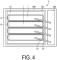
FIG. 4 is a schematic view for describing the semiconductor elements and a semiconductor device according to the embodiment. -
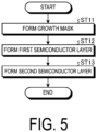
FIG. 5 is a flowchart for describing the manufacturing method for the semiconductor element according to the embodiment. -
FIG. 6 is a flowchart for describing a manufacturing method for the semiconductor device according to the embodiment. -
FIG. 7 is a cross-sectional schematic view for describing an example of a semiconductor element according to a first variation of the embodiment. -
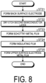
FIG. 8 is a flowchart for describing a manufacturing method for a semiconductor device according to the first variation of the embodiment. -
FIG. 9 is a cross-sectional schematic view for describing a semiconductor element according to a second variation of the embodiment. -
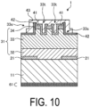
FIG. 10 is a cross-sectional schematic view for describing a semiconductor element according to a third variation of the embodiment. - An SBD manufactured using a free-standing GaN substrate may have crystal defects in various directions in a voltage resistant end portion of a surface on which an anode electrode is provided. When the crystal defects occur on the surface along a direction of an electric field in the voltage resistant end portion, an impurity level that serves as a source of leakage occurs even when the surface is covered with an insulating film. Thus, the crystal defects that occur along the direction of the electric field serve as paths for leakage current. This reduces the voltage resistance of the SBD.
- A manufacturing method for a
semiconductor element 1, thesemiconductor element 1, and asemiconductor device 2, according to the embodiment will be described below. Thesemiconductor element 1 is a power semiconductor used in switching circuits of power converters such as inverters and converters. -
FIG. 1 is a cross-sectional schematic view for describing the semiconductor element according to the embodiment.FIG. 2 is a cross-sectional schematic view for describing the manufacturing method for the semiconductor element and the semiconductor element according to the embodiment.FIG. 3 is a plan schematic view for describing the semiconductor element according to the embodiment.FIG. 4 is a schematic view for describing the semiconductor elements and the semiconductor device according to the embodiment. - As illustrated in
FIG. 1 to FIG. 3 , in thesemiconductor element 1 manufactured by the manufacturing method according to the embodiment, asemiconductor layer 31 is formed on asubstrate 11. In thesemiconductor layer 31, a GaN layer (first semiconductor layer) 32, which is an n+ type semiconductor layer, and a GaN layer (second semiconductor layer) 33, which is an n- type semiconductor layer, are layered in order from thesubstrate 11 side. Inside thesemiconductor element 1, amask 21 is interposed between thesubstrate 11 and theGaN layer 32. As illustrated inFIG. 4 , thesemiconductor device 2 includes thesemiconductor elements 1 manufactured in this manner. - The manufacturing method for the
semiconductor element 1 will be described with reference toFIGs. 1 ,2 , and5. FIG. 5 is a flowchart for describing the manufacturing method for the semiconductor element according to the embodiment. The manufacturing method for thesemiconductor element 1 is performed in accordance with steps illustrated inFIG. 5 . - The
substrate 11 illustrated inFIGs. 1 and2 is n+ type free-standing GaN. The doping amount of n-type impurities is controlled so that thesubstrate 11 has an electron carrier concentration of equal to or higher than 1018 cm-3. - A
back surface 11b on the opposite side to afront surface 1 1a of a GaN layer, which is a surface layer of thesubstrate 11, may be supported by a substrate other than the GaN substrate, such as a silicon substrate (not illustrated). The substrate that supports theback surface 11b of the GaN layer, which is the surface layer of thesubstrate 11, may be, for example, a sapphire substrate or a silicon carbide (SiC) substrate. - First, the
mask 21 made of SiO2 is formed on thefront surface 11a of the GaN layer, which is the surface layer of thesubstrate 11, illustrated inFIG. 2 (step ST11) (first step). More specifically, themask 21 having anopening 22 is provided on thefront surface 11a of thesubstrate 11. - The
mask 21 may contain an element that serves as a donor in thesemiconductor layer 31. Examples of a material of themask 21 may include metals such as W and Ti, nitrides such as SiN and AIN, and oxides such as Al2O3 and Ga2O3. Themask 21 may be amorphous. Themask 21 includes the opening 22. - A portion of the
front surface 11a of thesubstrate 11 corresponding to theopening 22 is exposed through the opening 22 of themask 21. Themask 21 may cover thefront surface 1 1a at both ends of thesubstrate 11. Themask 21 may cover the entire side surface or back surface of thesubstrate 11. Themask 21 may cover the entirety excluding the opening 22, of the surfaces that may come into contact with a raw material gas used in a vapor growth method, which will be described below. - A width w1 of the
mask 21 in a lateral direction orthogonal to a layering direction is, for example, 10 µm or more. The thickness of themask 21 in the layering direction is, for example, 100 nm. - As illustrated in
FIG. 2 , the GaN layer is formed as thesemiconductor layer 31 from thefront surface 1 1a of thesubstrate 11 exposed through theopening 22 using the ELO technique described above (step ST12) (second step). More specifically, using the ELO technique, an epitaxial apparatus (not illustrated) epitaxially grows GaN along themask 21 from thefront surface 1 1a of thesubstrate 11 exposed through theopening 22 to epitaxially grow an n+type GaN layer 32 with a high impurity concentration. - The
GaN layer 32 grows, from thefront surface 11a exposed through theopening 22, longitudinally above theopening 22 in the layering direction, and laterally outside theopening 22. Asurface 32a of the GaNlayer 32 becomes substantially flat. The GaNlayer 32 is auto-doped with impurities from the constituent material of themask 21 during crystal growth. When the impurity is silicon (Si), theGaN layer 32 is a highly doped n+ semiconductor layer. The doping amount of n-type impurities is controlled so that theGaN layer 32 has an electron carrier concentration equal to or higher than 1018 cm-3. When the doping amount is insufficient in auto-doping, an impurity (for example, Si) may be doped during epitaxial growth. The thickness of theGaN layer 32 in the layering direction is, for example, 10 µm or more. - In order to obtain a desired impurity concentration profile, the
GaN layer 33 with a low impurity concentration is formed so as to cover the GaN layer 32 (step ST13) (third step). More specifically, the n-type GaN layer 33 with a low impurity concentration is formed from thesurface 32a of theGaN layer 32. - The
GaN layer 33 is grown from thesurface 32a of theGaN layer 32 by selecting conditions in which longitudinal growth is dominant over lateral growth. Asurface 33a of theGaN layer 33 becomes substantially flat. Thesurface 33a of theGaN layer 33 is located on the opposite side to thesubstrate 11 in the layering direction and is a surface on which an upper surface electrode is provided. TheGaN layer 33 is an n- semiconductor layer. The doping amount of n-type impurities is controlled so that theGaN layer 33 has an electron carrier concentration lower than 1017 cm-3. During the epitaxial growth, theGaN layer 33 is not in contact with themask 21 and is covered with theGaN layer 32, so that the auto-doping is reduced. TheGaN layer 32 covers a large portion of themask 21, so that the auto-doping of theGaN layer 33 is also reduced. The thickness of the GaN layers 33 in the layering direction is, for example, 5 µm or more for an element with a breakdown voltage of 600 V. - As described above, as illustrated in
FIGs. 1 and2 , a semiconductor is epitaxially grown along themask 21 from thefront surface 11a exposed through theopening 22 to produce thesemiconductor element 1 including thesemiconductor layer 31. Thesemiconductor layer 31 is formed on thesubstrate 11. TheGaN layer 32, which is an n+ type semiconductor layer, and theGaN layer 33, which is an n- type semiconductor layer, are epitaxially grown from the front surface of thesubstrate 11 in the layering direction. - As illustrated in
FIG. 3 , thesemiconductor element 1 has a hexagonal shape when viewed from above in the layering direction. This is because the growth direction of the crystal in epitaxial growth is determined. In thesemiconductor layer 31 of thesemiconductor element 1, crystals grow longitudinally above theopening 22 in the layering direction, and laterally on the outside of theopening 22. As a result, the crystal defects on thesurface 33a of theGaN layer 33 of thesemiconductor element 1 extend longitudinally in the center portion, and extend laterally on the outside of the center portion. - A manufacturing method for the
semiconductor device 2 including thesemiconductor element 1 will be described with reference toFIG. 1 andFIG. 6. FIG. 6 is a flowchart for describing a manufacturing method for the semiconductor device according to the embodiment. The manufacturing method for thesemiconductor device 2 is performed in accordance with steps illustrated inFIG. 6 after thesemiconductor element 1 is manufactured in accordance with steps illustrated inFIG. 5 . Step ST21 to step ST22 are performed after performing step ST11 to step ST13. - Back
surface electrodes 61 are formed on theback surface 11b of thesubstrate 11 on the opposite side to the semiconductor layer 31 (step ST21). More specifically, theback surface electrodes 61 are formed on theback surface 11b of thesubstrate 11 by, for example, sputtering. - The
back surface electrodes 61 are obtained by, for example, performing Ti/Ni/Au plating on an Al layer. Note that theback surface electrodes 61 may be formed after aSchottky electrode 41, which will be described below, is formed. In the manufacturing method including a step of increasing a temperature, for example, by performing step ST21 last, the influence on theback surface electrodes 61 can be avoided. - The
Schottky electrode 41, which is a metal layer (barrier metal), is formed on thesurface 33a of theGaN layer 33 of the semiconductor layer 31 (step ST22). Thus, a Schottky junction is provided between theGaN layer 33 and theSchottky electrode 41. - The
Schottky metal film 41 is made of, for example, Ni, Al, or Pd. TheSchottky metal film 41 is located on the opposite side to thesubstrate 11 in the layering direction. TheSchottky metal film 41 is provided in the center portion of thesurface 33a of theGaN layer 33. A width w2 from an end portion of thesurface 33a of theGaN layer 33 to the Schottky metal film 41 (width of the voltage resistant end portion) is smaller than the width w1 of themask 21. On thesurface 33a of theGaN layer 33, an area from the end portion of thesurface 33a to theSchottky metal film 41 is referred to as a voltage resistant end portion. - In the above-described manner, the
semiconductor element 1 is manufactured. The manufacturedsemiconductor element 1 can be used as, for example, an SBD having a Schottky junction. Inside the manufacturedsemiconductor element 1, themask 21 is interposed between thesubstrate 11 and theGaN layer 32. - The manufacturing processes described above may be performed concurrently so as to simultaneously manufacture a plurality of
semiconductor elements 1. In this case, themask 21 is formed with a plurality ofopenings 22 in a striped pattern. By making onesemiconductor element 1 correspond to oneopening 22, the plurality ofsemiconductor elements 1 can be simultaneously made. - When the mask has a striped pattern, each crystal has a hexagonal shape with two long sides, and a cross-sectional view of the crystals with the two long sides is as illustrated in
FIG. 4 . - The
semiconductor elements 1 manufactured simultaneously may be separated into individual pieces and used in thesemiconductor devices 2, respectively. When the capacity needs to be increased, for example, while thesubstrate 11 and theback surface electrodes 61 are shared by the plurality ofsemiconductor elements 1, the plurality ofsemiconductor elements 1 may be mounted for use in thesemiconductor device 2, as illustrated inFIG. 4 . Specifically, as illustrated inFIG. 4 , theback surface electrodes 61 that are shared are each die-bonded to a corresponding one of theelectrode pads 201 on a mountingsubstrate 200, and individual upper surface electrode metal films (not illustrated) are connected to anotherelectrode pad 202 by bondingwires 52. By mounting the mountingsubstrate 200 in this manner, a plurality of diodes can be connected in parallel to increase the capacity and be used. At this time, the plurality ofsemiconductor elements 1 are manufactured so as to be aligned and disposed in a certain direction. In the layering direction view, thesemiconductor elements 1 each have a shape elongated in a substantially orthogonal direction with respect to a direction in which thesemiconductor elements 1 are aligned. Aligning thesemiconductor elements 1 having such a shape in this manner can increase a junction area of the diode. Thesemiconductor elements 1 manufactured in this manner are available for a variety ofsemiconductor devices 2 according to applications. - As described above, in the present embodiment, the
mask 21 is interposed between thesubstrate 11 and theGaN layer 32 inside thesemiconductor element 1. In the present embodiment, the width w2 from the end portion of thesurface 33a of theGaN layer 33 to theSchottky metal film 41 is smaller than the width w1 of themask 21. In the present embodiment, crystals grow longitudinally above theopening 22 in the layering direction, and laterally on the outside of theopening 22. In the present embodiment, the direction of crystal defects in the voltage resistant end portion is the lateral direction. As a result, according to the present embodiment, the occurrence of crystal defects along the direction of the electric field, which may serve as paths for leakage current of thesemiconductor element 1, can be reduced in the voltage resistant end portion. In the present embodiment, the voltage resistance of the SBD can be improved. - In the present embodiment, the width w1 of the
mask 21 is, for example, 10 µm or more. In this variation, the width w2 (< w1) of the voltage resistant end portion can be narrowed. According to this variation, the ratio of the conductive area of thesemiconductor element 1 can be increased. In the present embodiment, thesemiconductor element 1 can be reduced in size, thereby reducing costs. - A description is given of a first variation of the embodiment using
FIGs. 7 and8 .FIG. 7 is a cross-sectional schematic view for describing an example of a semiconductor element according to the first variation of the embodiment.FIG. 8 is a flowchart for describing a manufacturing method for a semiconductor device according to the first variation of the embodiment. As illustrated inFIG. 7 , thesemiconductor element 1 according to the first variation has a mesa structure and a field plate structure. Thesemiconductor device 2 includes such asemiconductor element 1. Note that inFIG. 7 , a step is drawn larger for description. The same applies to the following figures. - A manufacturing method for the
semiconductor device 2 including thesemiconductor element 1 will be described. Steps ST11 and ST12 are performed in a manner the same as or similar to that in the embodiment. In other words, thesemiconductor element 1 is manufactured in a manner the same as or similar to that in the embodiment. Step ST21 is performed in a manner the same as or similar to that in the embodiment. That is, after performing steps ST11 to ST21 in the embodiment, steps ST22 to ST25 are performed. - Part of the
GaN layer 33 is dry-etched (step ST22). More specifically, part of thesurface 33a of theGaN layer 33 is dry-etched. Specifically, a periphery of theGaN layer 33 is dry-etched. An end portion of thesurface 33a of theGaN layer 33 has a mesa structure. In other words, a periphery of the remainingGaN layer 33 has amesa step 33s. The periphery of theGaN layer 33 has asurface 33c at a position closer to theGaN layer 32 than thesurface 33a, in other words, at a position one step lower. - The
Schottky metal film 41 that forms a Schottky junction with theGaN layer 33 is formed on the exposedsurface 33a side (step ST23). TheSchottky metal film 41 covers the exposedsurface 33a of theGaN layer 33. Thus, the Schottky junction is provided between theGaN layer 33 and theSchottky metal film 41. - An insulating
film 42, which is an insulating layer, is formed (step ST24). The insulatingfilm 42 covers the exposedGaN layer 33 and a periphery of theSchottky metal film 41. The insulatingfilm 42 includes awall portion 421 covering the periphery of theSchottky metal film 41, awall portion 422 covering aside surface 33b of theGaN layer 33, and awall portion 423 covering thesurface 33c of theGaN layer 33. Thewall portion 421 has an opening that exposes theSchottky metal film 41 in the center portion. Thewall portion 422 extends downward in the layering direction from an outer end portion of thewall portion 421. Thewall portion 423 extends outward from a lower end portion of thewall portion 422 in the layering direction. - An upper surface
electrode metal film 43 is formed on theSchottky metal film 41 and on the insulating film 42 (step ST25). The upper surfaceelectrode metal film 43 forms a so-called field plate on the insulatingfilm 42. An outer end portion of thewall portion 423 of the insulatingfilm 42 is not covered with the upper surfaceelectrode metal film 43. - Step ST21, which is a step of forming the back surface electrode, may be performed after step ST25 when the annealing temperature of the back surface electrode does not affect the
Schottky metal film 41, the insulatingfilm 42, and the upper surfaceelectrode metal film 43. - In the above-described manner, the
semiconductor element 1 having the mesa structure and the field plate structure is manufactured. Having the field plate can reduce the electric field applied to the end portion of the upper surface electrode, resulting in a device with high breakdown voltage. The field plate may be separated from the upper electrode. - In this variation, the electric field applied to the end portion of the upper surface electrode can be reduced by having the
mesa step 33s. In this variation, the electric field applied to the end portion of the upper surface electrode can be reduced by having the field plate. Thus, according to this variation, thesemiconductor element 1 with a high maximum peak current can be manufactured. According to this variation, thesemiconductor element 1 with improved voltage resistance can be manufactured. - In this variation, the crystal direction in the voltage resistant end portion is the lateral direction, and the occurrence of crystal defects on the surface along the electric field direction, which may serve as paths for leakage current in the
semiconductor element 1, can be reduced. Thus, in this variation, the height of themesa step 33s in the layering direction can be reduced. In this variation, the width w2 of the voltage resistant end portion can be narrowed. These allow the ratio of the conductive area of thesemiconductor element 1 to be increased in this variation. According to the present embodiment, thesemiconductor element 1 can be smaller, thereby reducing costs. - A description is given of a second variation of the embodiment using
FIG. 9. FIG. 9 is a cross-sectional schematic view for describing a semiconductor element according to the second variation of the embodiment. Thesemiconductor element 1 according to the second variation has a mesa structure, a field plate structure, and a trench structure. - A manufacturing method for the
semiconductor device 2 including thesemiconductor element 1 will be described. Step ST11 to step ST13 are performed in a manner the same as or similar to that in the embodiment. In other words, thesemiconductor element 1 is manufactured in a manner the same as or similar to that in the embodiment. Step ST21 is performed in a manner the same as or similar to that in the embodiment. That is, after performing steps ST11 to ST21 in the embodiment, steps ST22 to ST25 are performed. In the following, steps different from those in the first variation will be described. - In step ST22, the
mesa step 33s and atrench structure 33t are formed in theGaN layer 33 by dry etching. More specifically, a periphery of the remainingGaN layer 33 has themesa step 33s. Thetrench structure 33t having a groove shape is formed inside the periphery of the remainingGaN layer 33. In theGaN layer 33, part of thesurface 33a remains except for the area where themesa step 33s or thetrench structure 33t is formed. - In step ST23, the
Schottky metal film 41 is formed on thesurface 33a remaining inside themesa step 33s. - In step ST24, the insulating
film 42 is formed to cover the exposed surface of theGaN layer 33 that is not covered with theSchottky metal film 41. - In step ST 25, the upper surface
electrode metal film 43 is formed on theSchottky metal film 41 and on the insulatingfilm 42. - In the above-described manner, the
semiconductor element 1 having the mesa structure, the field plate structure, and the trench structure is manufactured. - In this variation, the electric field applied to the center portion of the upper surface electrode can be reduced by having the trench structure. According to this variation, the
semiconductor element 1 with higher voltage resistance can be manufactured. - A description is given of a third variation of the embodiment using
FIG. 10. FIG. 10 is a cross-sectional schematic view for describing a semiconductor element according to the third variation of the embodiment. Thesemiconductor element 1 according to the third variation has a mesa structure, a field plate structure, and a JBS structure. According to the third variation, in thesemiconductor layer 31 of thesemiconductor element 1, the GaN layer (first semiconductor layer) 32, which is an n+ type semiconductor layer, the GaN layer (second semiconductor layer) 33, which is an n- type semiconductor layer, and a GaN layer (first semiconductor layer) 34, which is a p+ type semiconductor layer, are layered in order from thesubstrate 11. - A manufacturing method for the
semiconductor device 2 including thesemiconductor element 1 will be described. In the third variation, after performing step ST11 to step ST13, step ST14 (not shown) is performed. - In order to obtain a desired higher purity concentration profile, the p+
type GaN layer 34 with a high impurity concentration is formed to cover the GaN layer 33 (step ST14). - The doping amount of p-type impurities is controlled so that the
GaN layer 34 has a hole carrier concentration of equal to or higher than 1018 cm-3. The surface of theGaN layer 34 becomes substantially flat. The thickness of theGaN layer 34 in the layering direction is, for example, 20 nm or more. - Steps ST21 and ST25 are performed in a manner the same as or similar to that in the second variation.
- In step ST22, part of the
GaN layer 34 and part of theGaN layer 33 are dry-etched to form themesa step 33s and thetrench structure 33t. - In step ST23, the
Schottky metal film 41 is formed on theGaN layer 34 and theGaN layer 33, which are exposed inside themesa step 33s and outside theGaN layer 34 and theGaN layer 33 left in the center. In other words, theSchottky metal film 41 is disposed except for the center portion and the end portion when viewed in the layering direction. - In step ST24, the insulating
film 42 is formed to cover the exposed surface of theGaN layer 33 that is not covered with theSchottky metal film 41. - In the above-described manner, the
semiconductor element 1 having the mesa structure, the field plate structure, and the JBS structure is manufactured. Note that thesemiconductor element 1 having the JBS structure is not limited thereto. For example, thesemiconductor element 1 may be a Schottky barrier diode. - In this variation, the electric field applied to the center portion of the upper surface electrode can be reduced by having the JBS structure. According to this variation, the
semiconductor element 1 with higher voltage resistance can be manufactured. In this variation, the leakage current can be reduced. - The embodiment disclosed by the present application can be modified without departing from the main point or the scope of the present invention. The embodiment and variations thereof disclosed in the present application can be combined as appropriate.
- Embodiments have been described in order to fully and clearly disclose the technology according to the appended claims. However, the appended claims are not to be limited to the embodiments described above and may be configured to embody all variations and alternative configurations that those skilled in the art may make within the underlying matter set forth herein.
-
- 1 Semiconductor element
- 2 Semiconductor device
- 11 Substrate
- 11a Front surface
- 21 Mask
- 22 Opening
- 31 Semiconductor layer
- 32 GaN layer (first semiconductor layer)
- 33 GaN layer (second semiconductor layer)
- 61 Back surface electrode
- 200 Mounting substrate
- 201 Electrode pad
- 202 Electrode pad
Claims (10)
- A method of manufacturing a semiconductor element, the method comprising:forming a mask on a front surface of a substrate, the mask having an opening to expose the front surface;growing a first semiconductor layer by epitaxially growing a semiconductor along the mask, starting from the front surface exposed through the opening; andgrowing a second semiconductor layer on a surface located opposite to the substrate in a layering direction; andproviding an electrode located opposite to the surface of the first semiconductor layer in the layering direction, whereina width from an end portion of the surface to the electrode is smaller than a width of the mask.
- The method of manufacturing a semiconductor element according to claim 1, wherein
the width of the mask is 10 µm or more. - The method of manufacturing a semiconductor element according to claim 1 or 2, comprising:
having a mesa structure at an end portion of the surface located on an opposite side to the substrate in the layering direction and on which the electrode is provided. - The method of manufacturing a semiconductor element according to any one of claims 1 to 3, comprising:
having a field plate structure. - The method of manufacturing a semiconductor element according to any one of claims 1 to 3, comprising:
having a trench structure. - The method of manufacturing a semiconductor element according to any one of claims 1 to 3, comprising:
having a JBS structure. - The method of manufacturing a semiconductor element according to any one of claims 1 to 6, wherein
the first semiconductor layer and the second semiconductor layer are hexagonal when viewed in the layering direction. - The method of manufacturing a semiconductor element according to any one of claims 1 to 7, wherein
the mask is interposed between the substrate and the first semiconductor layer inside the semiconductor element. - A semiconductor element manufactured by the method of manufacturing a semiconductor element according to any one of claims 1 to 8, wherein
the mask is interposed between the substrate and the first semiconductor layer inside the semiconductor element. - A semiconductor device comprising:
a semiconductor element manufactured by the method of manufacturing a semiconductor element according to any one of claims 1 to 8.
Applications Claiming Priority (2)
| Application Number | Priority Date | Filing Date | Title |
|---|---|---|---|
| JP2020209672 | 2020-12-17 | ||
| PCT/JP2021/044789 WO2022131059A1 (en) | 2020-12-17 | 2021-12-06 | Method for manufacturing semiconductor element, semiconductor element, and semiconductor device |
Publications (1)
| Publication Number | Publication Date |
|---|---|
| EP4266350A1 true EP4266350A1 (en) | 2023-10-25 |
Family
ID=82057670
Family Applications (1)
| Application Number | Title | Priority Date | Filing Date |
|---|---|---|---|
| EP21906422.7A Withdrawn EP4266350A1 (en) | 2020-12-17 | 2021-12-06 | Method for manufacturing semiconductor element, semiconductor element, and semiconductor device |
Country Status (5)
| Country | Link |
|---|---|
| US (1) | US20230326993A1 (en) |
| EP (1) | EP4266350A1 (en) |
| JP (1) | JPWO2022131059A1 (en) |
| CN (1) | CN116569338A (en) |
| WO (1) | WO2022131059A1 (en) |
Family Cites Families (10)
| Publication number | Priority date | Publication date | Assignee | Title |
|---|---|---|---|---|
| JP4667556B2 (en) * | 2000-02-18 | 2011-04-13 | 古河電気工業株式会社 | Vertical GaN-based field effect transistor, bipolar transistor and vertical GaN-based field effect transistor manufacturing method |
| JP2009076866A (en) * | 2007-08-31 | 2009-04-09 | Sumitomo Electric Ind Ltd | Schottky barrier diode |
| JP5681937B2 (en) * | 2010-11-25 | 2015-03-11 | 株式会社パウデック | Semiconductor device and manufacturing method thereof |
| JP2012124268A (en) * | 2010-12-07 | 2012-06-28 | Nippon Inter Electronics Corp | Semiconductor device |
| JP5888214B2 (en) * | 2012-11-30 | 2016-03-16 | 富士電機株式会社 | Nitride-based compound semiconductor device and manufacturing method thereof |
| JP6070422B2 (en) | 2013-05-31 | 2017-02-01 | 豊田合成株式会社 | Semiconductor device manufacturing method and semiconductor device |
| JP5940500B2 (en) * | 2013-09-11 | 2016-06-29 | 株式会社東芝 | Semiconductor device and manufacturing method thereof |
| JP2015099903A (en) * | 2013-10-17 | 2015-05-28 | ローム株式会社 | Nitride semiconductor device and manufacturing method of the same |
| JP2016031953A (en) * | 2014-07-25 | 2016-03-07 | 株式会社タムラ製作所 | Semiconductor device and method for manufacturing the same, semiconductor substrate, and crystal laminate structure |
| CN112204754B (en) * | 2018-05-30 | 2024-08-13 | 加利福尼亚大学董事会 | Method for removing a semiconductor layer from a semiconductor substrate |
-
2021
- 2021-12-06 JP JP2022569881A patent/JPWO2022131059A1/ja active Pending
- 2021-12-06 EP EP21906422.7A patent/EP4266350A1/en not_active Withdrawn
- 2021-12-06 CN CN202180082891.8A patent/CN116569338A/en active Pending
- 2021-12-06 WO PCT/JP2021/044789 patent/WO2022131059A1/en not_active Ceased
-
2023
- 2023-06-13 US US18/333,747 patent/US20230326993A1/en active Pending
Also Published As
| Publication number | Publication date |
|---|---|
| US20230326993A1 (en) | 2023-10-12 |
| WO2022131059A1 (en) | 2022-06-23 |
| CN116569338A (en) | 2023-08-08 |
| JPWO2022131059A1 (en) | 2022-06-23 |
Similar Documents
| Publication | Publication Date | Title |
|---|---|---|
| US12283627B2 (en) | Semiconductor device having a gate insulating layer | |
| US7679104B2 (en) | Vertical type semiconductor device and manufacturing method of the device | |
| TWI395320B (en) | Gallium nitride semiconductor device | |
| CN110249432B (en) | Semiconductor devices for power | |
| US7605441B2 (en) | Semiconductor device | |
| JP6104575B2 (en) | Semiconductor device | |
| EP2369626A2 (en) | Semiconductor element | |
| JP2024144777A (en) | Semiconductor Device | |
| TW201234538A (en) | Gallium nitride power devices using island topography | |
| US8823148B2 (en) | Diode with epitaxially grown semiconductor layers | |
| JP2018182234A (en) | Silicon carbide semiconductor device and method of manufacturing silicon carbide semiconductor device | |
| TW200525783A (en) | Light-emitting semiconductor device and method of fabrication | |
| US8178940B2 (en) | Schottky barrier diode and method for using the same | |
| WO2016170978A1 (en) | Semiconductor device | |
| JP6428900B1 (en) | Diode element and method for manufacturing diode element | |
| JP2020202404A (en) | Semiconductor device and manufacturing method thereof | |
| JP5682102B2 (en) | Vertical gallium nitride semiconductor device with reverse breakdown voltage | |
| US20190333998A1 (en) | Silicon carbide epitaxial wafer and silicon carbide semiconductor device | |
| JP6932998B2 (en) | Silicon Carbide MOSFET and its manufacturing method | |
| JP5362187B2 (en) | Semiconductor element | |
| EP4266350A1 (en) | Method for manufacturing semiconductor element, semiconductor element, and semiconductor device | |
| US10170561B1 (en) | Diamond semiconductor device | |
| US20230163221A1 (en) | Schottky barrier diode and method for manufacturing same | |
| JP2022186426A (en) | Semiconductor device and manufacturing method thereof | |
| WO2021124549A1 (en) | Semiconductor element and semiconductor element manufacturing method |
Legal Events
| Date | Code | Title | Description |
|---|---|---|---|
| STAA | Information on the status of an ep patent application or granted ep patent |
Free format text: STATUS: THE INTERNATIONAL PUBLICATION HAS BEEN MADE |
|
| PUAI | Public reference made under article 153(3) epc to a published international application that has entered the european phase |
Free format text: ORIGINAL CODE: 0009012 |
|
| STAA | Information on the status of an ep patent application or granted ep patent |
Free format text: STATUS: REQUEST FOR EXAMINATION WAS MADE |
|
| 17P | Request for examination filed |
Effective date: 20230614 |
|
| AK | Designated contracting states |
Kind code of ref document: A1 Designated state(s): AL AT BE BG CH CY CZ DE DK EE ES FI FR GB GR HR HU IE IS IT LI LT LU LV MC MK MT NL NO PL PT RO RS SE SI SK SM TR |
|
| DAV | Request for validation of the european patent (deleted) | ||
| DAX | Request for extension of the european patent (deleted) | ||
| STAA | Information on the status of an ep patent application or granted ep patent |
Free format text: STATUS: THE APPLICATION HAS BEEN WITHDRAWN |
|
| 18W | Application withdrawn |
Effective date: 20240328 |