EP4261602A1 - Optische vorrichtung mit phasenwechselmaterial und zugehörige verfahren - Google Patents
Optische vorrichtung mit phasenwechselmaterial und zugehörige verfahren Download PDFInfo
- Publication number
- EP4261602A1 EP4261602A1 EP23167252.8A EP23167252A EP4261602A1 EP 4261602 A1 EP4261602 A1 EP 4261602A1 EP 23167252 A EP23167252 A EP 23167252A EP 4261602 A1 EP4261602 A1 EP 4261602A1
- Authority
- EP
- European Patent Office
- Prior art keywords
- optical
- pcm
- layer
- pcm layer
- optical fiber
- Prior art date
- Legal status (The legal status is an assumption and is not a legal conclusion. Google has not performed a legal analysis and makes no representation as to the accuracy of the status listed.)
- Pending
Links
Images




Classifications
-
- G—PHYSICS
- G02—OPTICS
- G02F—OPTICAL DEVICES OR ARRANGEMENTS FOR THE CONTROL OF LIGHT BY MODIFICATION OF THE OPTICAL PROPERTIES OF THE MEDIA OF THE ELEMENTS INVOLVED THEREIN; NON-LINEAR OPTICS; FREQUENCY-CHANGING OF LIGHT; OPTICAL LOGIC ELEMENTS; OPTICAL ANALOGUE/DIGITAL CONVERTERS
- G02F1/00—Devices or arrangements for the control of the intensity, colour, phase, polarisation or direction of light arriving from an independent light source, e.g. switching, gating or modulating; Non-linear optics
- G02F1/0009—Materials therefor
- G02F1/0054—Structure, phase transitions, NMR, ESR, Moessbauer spectra
-
- G—PHYSICS
- G02—OPTICS
- G02F—OPTICAL DEVICES OR ARRANGEMENTS FOR THE CONTROL OF LIGHT BY MODIFICATION OF THE OPTICAL PROPERTIES OF THE MEDIA OF THE ELEMENTS INVOLVED THEREIN; NON-LINEAR OPTICS; FREQUENCY-CHANGING OF LIGHT; OPTICAL LOGIC ELEMENTS; OPTICAL ANALOGUE/DIGITAL CONVERTERS
- G02F1/00—Devices or arrangements for the control of the intensity, colour, phase, polarisation or direction of light arriving from an independent light source, e.g. switching, gating or modulating; Non-linear optics
- G02F1/29—Devices or arrangements for the control of the intensity, colour, phase, polarisation or direction of light arriving from an independent light source, e.g. switching, gating or modulating; Non-linear optics for the control of the position or the direction of light beams, i.e. deflection
- G02F1/31—Digital deflection, i.e. optical switching
- G02F1/313—Digital deflection, i.e. optical switching in an optical waveguide structure
- G02F1/3131—Digital deflection, i.e. optical switching in an optical waveguide structure in optical fibres
-
- G—PHYSICS
- G02—OPTICS
- G02F—OPTICAL DEVICES OR ARRANGEMENTS FOR THE CONTROL OF LIGHT BY MODIFICATION OF THE OPTICAL PROPERTIES OF THE MEDIA OF THE ELEMENTS INVOLVED THEREIN; NON-LINEAR OPTICS; FREQUENCY-CHANGING OF LIGHT; OPTICAL LOGIC ELEMENTS; OPTICAL ANALOGUE/DIGITAL CONVERTERS
- G02F1/00—Devices or arrangements for the control of the intensity, colour, phase, polarisation or direction of light arriving from an independent light source, e.g. switching, gating or modulating; Non-linear optics
- G02F1/0009—Materials therefor
- G02F1/009—Thermal properties
-
- G—PHYSICS
- G02—OPTICS
- G02F—OPTICAL DEVICES OR ARRANGEMENTS FOR THE CONTROL OF LIGHT BY MODIFICATION OF THE OPTICAL PROPERTIES OF THE MEDIA OF THE ELEMENTS INVOLVED THEREIN; NON-LINEAR OPTICS; FREQUENCY-CHANGING OF LIGHT; OPTICAL LOGIC ELEMENTS; OPTICAL ANALOGUE/DIGITAL CONVERTERS
- G02F1/00—Devices or arrangements for the control of the intensity, colour, phase, polarisation or direction of light arriving from an independent light source, e.g. switching, gating or modulating; Non-linear optics
- G02F1/01—Devices or arrangements for the control of the intensity, colour, phase, polarisation or direction of light arriving from an independent light source, e.g. switching, gating or modulating; Non-linear optics for the control of the intensity, phase, polarisation or colour
- G02F1/011—Devices or arrangements for the control of the intensity, colour, phase, polarisation or direction of light arriving from an independent light source, e.g. switching, gating or modulating; Non-linear optics for the control of the intensity, phase, polarisation or colour in optical waveguides, not otherwise provided for in this subclass
- G02F1/0115—Devices or arrangements for the control of the intensity, colour, phase, polarisation or direction of light arriving from an independent light source, e.g. switching, gating or modulating; Non-linear optics for the control of the intensity, phase, polarisation or colour in optical waveguides, not otherwise provided for in this subclass in optical fibres
-
- G—PHYSICS
- G02—OPTICS
- G02F—OPTICAL DEVICES OR ARRANGEMENTS FOR THE CONTROL OF LIGHT BY MODIFICATION OF THE OPTICAL PROPERTIES OF THE MEDIA OF THE ELEMENTS INVOLVED THEREIN; NON-LINEAR OPTICS; FREQUENCY-CHANGING OF LIGHT; OPTICAL LOGIC ELEMENTS; OPTICAL ANALOGUE/DIGITAL CONVERTERS
- G02F1/00—Devices or arrangements for the control of the intensity, colour, phase, polarisation or direction of light arriving from an independent light source, e.g. switching, gating or modulating; Non-linear optics
- G02F1/01—Devices or arrangements for the control of the intensity, colour, phase, polarisation or direction of light arriving from an independent light source, e.g. switching, gating or modulating; Non-linear optics for the control of the intensity, phase, polarisation or colour
- G02F1/0147—Devices or arrangements for the control of the intensity, colour, phase, polarisation or direction of light arriving from an independent light source, e.g. switching, gating or modulating; Non-linear optics for the control of the intensity, phase, polarisation or colour based on thermo-optic effects
-
- G—PHYSICS
- G02—OPTICS
- G02F—OPTICAL DEVICES OR ARRANGEMENTS FOR THE CONTROL OF LIGHT BY MODIFICATION OF THE OPTICAL PROPERTIES OF THE MEDIA OF THE ELEMENTS INVOLVED THEREIN; NON-LINEAR OPTICS; FREQUENCY-CHANGING OF LIGHT; OPTICAL LOGIC ELEMENTS; OPTICAL ANALOGUE/DIGITAL CONVERTERS
- G02F2202/00—Materials and properties
- G02F2202/10—Materials and properties semiconductor
Definitions
- the present invention relates to the field of optics, and, more particularly, to optical switches and related methods.
- Optical systems regularly use active devices to control or switch optical power or signals on demand.
- Most available materials used in optical devices and associated switches are considered "non-latching.” Examples include non-linear optical devices such as liquid crystals that may react to changes in electric fields, thermo-optic devices that may react to changes in temperature, and piezo-optic devices that may react to changes in mechanical strain.
- Many conventional non-latching optical switching devices use an optical signal for control and function as non-linear optics under intense laser power.
- Some optical switches are formed from discrete optical and electronic components, or are formed as photonic integrated circuit (PIC) structures based on semiconductor wafer fabrication processes. Discrete optical switches tend to be large, and use a separate electrical power source to operate. For a PIC, a large power penalty occurs going from the optical fiber into the PIC and back out of the PIC into another optical fiber. These losses may be greater than one decibel.
- PIC photonic integrated circuit
- optical materials that can vary their refractive index and maintain a set index of refraction without using an outside power source for continuous latching.
- Many optical devices thus employ polarizable materials such as liquid crystals, lithium niobate (LiNbO 3 ) materials, or piezo-optic materials. Devices made from these materials are typically slow and may be anisotropic and birefringent, thus making them polarization dependent and non-latching.
- Most electric field or optically switched materials have a relatively small index change of less than about 0.01, or are orders of magnitude smaller.
- Some optical devices employ chalcogenides for an X 3 photo refractive effect, but not for the optical benefits of a phase change. Those chalcogenides used for their phase change properties are commonly used in electronic or optical memories and have not been reliable as an active optical material due to absorption or large index values. Other optical devices may couple chalcogenide materials with mechanical mechanisms, such as an actuator, or a microelectromechanical device, but these optical devices are limited because of their use of an external actuator or MEMS device.
- an optical device may comprise at least one optical fiber, and a phase change material (PCM) layer on the at least one optical fiber.
- the PCM layer may comprise Ge x Se y , where x is in a range of 20-40 and y is in a range of 60-80.
- x is in a range of 30-40, and y is in a range of 60-70.
- a heat source may be thermally coupled to the PCM layer to selectively change the phase of the PCM layer.
- the heat source may comprise an optical energy source coupled to the at least one optical fiber and operable at a different wavelength for heating than a wavelength for signal transmission.
- An electrically conductive layer may be on the at least one optical fiber and electrically coupled to the PCM layer to selectively change the phase of the PCM layer.
- the at least one optical fiber may comprise a single mode optical fiber.
- the at least one optical fiber may comprise a plurality of optical fibers laterally joined together to define an optical switching portion.
- the PCM layer may be on the optical switching portion so that a phase of the PCM layer determines a latched switch state from among a plurality of latched switch states.
- the plurality of latched switch states may correspond to a plurality of different continuous optical fiber signal paths.
- the optical switching portion may have a tapered diameter shape.
- the method includes forming a phase change material (PCM) layer on at least one optical fiber.
- the PCM layer may comprise Ge x Se y , where x is in a range of 20-40, and y is in a range of 60-80.
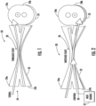
- FIGS. 1 and 2 there is illustrated generally at 20, an optical device formed in this example as an optical switch having a plurality of latched switch states.
- a plurality of optical fibers 24 are laterally joined together to define an optical switching portion 28, and in this example formed as a tapered diameter shape.
- two optical fibers 24a,24b are laterally joined together with a first optical fiber 24a being a through fiber through which an initial optical signal is transmitted ( FIG. 1 ), and a second optical fiber 24b acting as the drop fiber to which the optical signal may be switched via a control signal 30 such as an optical pulse ( FIG. 2 ).
- At least one phase change material (PCM) layer 32 is formed on the optical switching portion 28.
- the phase of the PCM layer may determine a latched switch state from among the plurality of latched switch states, which may be changed by application of heat from a heat source 33 as explained further below such as generated from an optical, thermal or electrical energy source.
- a heat source 33 such as generated from an optical, thermal or electrical energy source.
- the plurality of latched switch states corresponds to a plurality of different continuous optical fiber signal paths, and in this example, changing from the through or first optical fiber 24a into the second optical fiber 24b, also termed the drop fiber through which the control signal 30 passes.
- the end views of the optical switch 20 in FIGS. 1 and 2 are illustrated at the right and show in the through state of FIG. 1 the optical signal passing through the first optical fiber 24a shown by the "plus” sign on the right.
- the switched state is shown in FIG. 2
- the phase of the PCM layer 32 changes the latched state so that the optical signal passes from the through or first optical fiber 24a into the drop or second optical fiber 24b as shown by the plus sign in the second fiber of FIG. 2 .
- the PCM layer 32 in the end view of FIG. 2 includes hash lines indicating a phase change.
- the control signal 30, as a separate optical signal supplies optical energy to the optical switching portion 28, which may be a different wavelength for heating than a wavelength for signal transmission.
- a wavelength below approximately 700 nm, where the PCM starts to significantly absorb light may be optimum for thermal processes to initiate a phase change created by thermal heat in the PCM layer 32.
- a wavelength between about 700 nm and 430 nm is possible.
- the long wavelength limit is defined by the onset of absorption of the light by the PCM and the lower wavelength limit is defined by the transmission or absorption of the transporting waveguide, the example here being SiO2 glass fiber.
- either one of the first and second optical fibers 24a,24b may be configured to supply optical energy to the optical switching portion 28 to selectively change the phase of the PCM layer 32.
- An optical energy source 34 ( FIG. 6 ), such as a laser or other source of optical energy, may be coupled to at least one of the plurality of optical fibers 24 and operable at a different wavelength for heating than a wavelength for signal transmission. In the example shown in FIG. 6 , the optical energy source 34 is coupled to the second optical fiber 24b as the drop fiber.
- Each of the plurality of optical fibers 24 may be formed as a single mode optical fiber, but depending on the end use requirements, one or more of the optical fibers may be formed as a multimodal optical fiber.
- the control signal 30 provides the optical energy, and resultant heat, to change the phase of the PCM layer 32 that is formed on one side of the optical switching portion 28 forming the optical switch 20.
- the optical phase matching condition of this optical device as an optical switch 20 is altered and the optical signal switches from the first optical fiber 24a to the second optical fiber 24b.
- the control signal in this example as the light from the optical energy source 34 FIG. 6
- the optical device, in this example the optical switch 20 remains latched until the process is reversed.
- the PCM layer 32 is preferably formed from a chalcogenide as a chemical compound and includes a sulfide, selenide, telluride, or polonide. It is a material that when in the correct stoichiometry range is transparent at optical telecommunication wavelengths, such as a wavelength range of 1,260 nm to 1,625 nm, and in an example, the commercially well-known 1,300 and 1,550 nanometer bands, although wavelengths as low as about 850 nm are possible.
- the PCM layer 32 may switch variably between two index values using electrical, thermal, or optical energy. The phase changes may occur between the temperatures giving a full molten state and temperatures giving crystallization.
- This material as the PCM layer 32 latches and remains in a given state upon removal of power, and has a much lower index of refraction than the more conventional phase change materials used with electronic or optical memories, for example.
- This material as the PCM layer 32 is more readily configured into optical devices that use traditional optical materials with low index values, such as the illustrated optical switch 20.
- This optically transparent chalcogenide glass may have a general formulation and stoichiometry of Gex Se 100-x within the range as noted above.
- This material as the PCM layer 32 may provide changes in a large index of refraction greater than 10%, but remain in a given latched state indefinitely.
- the PCM layer 32 takes advantage of the thermally induced structural phase changes to vary the index of refraction, which is switchable and reversible, and remains latched in a given state once switched. It is low-loss in the telecom wavelengths in both states.
- the PCM layer 32 may be formed on about half of an optical fiber 24, in this example, about 50% of the optical fiber by directionally coating the PCM material onto the optical fiber, which in the illustrated example of FIGS. 1 and 2 is the second optical fiber 24b.
- the PCM layer 32 may be coated for length of about 0.1 to 20 millimeters along the length of the optical fiber 24b at a depth of a few nanometers thickness, and in a non-limiting example, about no greater than 40 nm to prevent the PCM layer from becoming a waveguide itself.
- the optical fiber 24 is shown having an optical mode field in the central portion of the optical fiber with an N of about 2.4.
- the change in phase of the PCM layer 32 with an N of about 2.7 moves the mode field to an upper region of only a few micrometers in the optical fiber 24 to implement a latched switch state.
- the sectional, schematic view in FIG. 7 of multiple optical fibers 24 illustrates different exposures created by the optical energy from an optical energy source 34 ( FIG. 6 ) that induces a phase change.
- the schematic views in FIG. 7 show alternating bright, dark, bright exposures that allow switching back and forth in the optical switch 20 between different latched switch states.
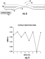
- an electrical source 42 and a conductive layer 40 ( FIG. 8 ) on at least one of the plurality of optical fibers 24 and electrically coupled to the PCM layer 32 to selectively change the phase of the PCM layer at the optical switch 20.
- the optical fiber 24, in this example the drop or second optical fiber 24b is coated with an electrically conductive layer 40 such as gold at about a few microns thickness such as about 2-3 microns as a non-limiting example.
- the distance along the optical fiber 24b to which the PCM layer 32 will be applied may have its electrically conductive layer 40 removed, and the PCM layer applied such as by various coating technologies. That optical fiber 24b section having the electrically conductive layer 40 removed and the PCM layer 32 applied, is joined laterally with another optical fiber, in this example, the first optical fiber 24a, to form the optical device as an optical switch 20 shown in FIG. 8 .
- FIG. 9 An example for the electrically induced phase change as imparted by an electrical signal directed along the electrically conductive layer 40 into the PCM layer 32 is shown by the graph of FIG. 9 , where the current in amperes is shown on the vertical axis and the switch cycle for the latched switch state changes back-and-forth in 7 cycles, shown on the horizontal axis. The graph shows that ohmic heating from an electrical current is able to change the phase of the PCM layer 32.
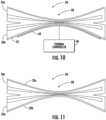
- a heat source 44 may be thermally coupled to the PCM layer 32 to selectively change the phase of the PCM layer as shown in the example of the optical switch 20 in FIG. 10 .
- a thermal heat controller 46 connected to the heat source 44 controls thermal heating onto the PCM layer 32. The heat may be generated for only a few nanoseconds, for example, from 1 or 2 nanoseconds up to 10's of nanoseconds, to create the phase change.
- the PCM layer 32 may be formed as first and second PCM layers 32a,32b on opposite sides of the optical switching portion 28 as shown in FIG. 11 .
- Each of the PCM layers 32a,32b may be used to determine a latched switch state by applying heat via an optical signal into the respective optical fiber 24a,24b using an optical energy source 34, such as in FIG. 6 , or an electrical signal applied via an electrically conductive layer 40 such as in FIG. 8 , or a separate heat source 44 as in FIG. 10 .
- the optical switch 20' includes four optical fibers 24a', 24b', 24c', 24d' and first and second PCM layers 32a', 32b' are on opposite sides of the optical switching portion 28' formed from the tapered area of the four optical fibers.
- An optical input to the optical switch 20' may include two separate optical signal inputs, with a first optical signal entering optical fiber 24b', and the second optical signal entering optical fiber 24c'. These may be selectively switched into two different outputs as two different signal paths.
- the optical control signal 50' may be generated from an optical signal, electric current, or thermal heating as in FIGS. 6 , 8 , and 10 .
- a plurality of optical switches 20 are arranged in a switched array illustrated generally at 54, where each optical switch 20 has a plurality of latched switch states.
- This switched array 54 forms an optical device that may operate similar to a field programmable gate array (FPGA) and have one input 58 in this example.
- Each optical switch 20 includes a PCM layer 32 that may latch the respective optical switch into a different state using a control signal 60 applied at each optical switch as illustrated.
- the control signal 60 may be an optical signal, a thermally generated input to a heat source, or electrical power signal along conductive layer such as shown in respective FIGS. 6 , 8 , and 10 .
- An example PCM layer 32 may be formed from Ge 30 Se 70 as noted before.
- the graph in FIG. 14 shows the refractive index relative to the wavelength in nanometers at different temperatures for the PCM layer 32 formed with the stoichiometry ratio Ge 30 Se 70 , ranging from 20°C as shown by the line at A up to about 470°C as shown by the line at F. This range between the lines at the 1,600 nanometers mark illustrates the low refractive index with a large index variation of the PCM layer 32.
- An example single mode fiber may be used for the optical fibers 24 and have about 125 micron cladding and an 8-10 micron core.
- the diameter of the optical switching portion may be reduced to about 10 microns to 40 microns with the tapered diameter shape.
- FIG. 15 a high-level flowchart illustrates an example of making an optical device as an optical switch 20 and illustrated generally at 100. General steps are described first relative to the flowchart, followed by a more detailed process flow description.
- phase change material (PCM) layer 32 is formed on at least one optical fiber 24 (Block 104 ).
- This PCM layer 32 may comprise a chalcogenide material, and in an example, Ge X Se Y , where X is in the range of about 20-40, and Y is in the range of about 60-80.
- This optical fiber 24 may be laterally joined with another optical fiber to define an optical switching portion 28 (Block 106 ). Energy may be applied to the optical switching portion 28 to selectively change the phase of the PCM layer 32, such as using an electrically coupled conductive layer, a heat source thermally coupled to the PCM layer, or optical signal energy (Block 108 ).
- the process ends (Block 110 ).
- the process would start with the fusing of the glass and pulling a taper (very high temperatures). Then the process may include directionally coating one side of the fiber/coupler with the PCM that cannot withstand the high temperatures of the tapering process, e.g., using a fused biconical taper coupler process, which is the most prevalent in industry.
- Another method in line with the description would be to use polished or "D"-shaped fibers to access close to the core regions and deposit PCM on one of the faces prior to gluing the two faces together. A polished and glued coupler is not very prevalent in industry.
Landscapes
- Physics & Mathematics (AREA)
- Nonlinear Science (AREA)
- General Physics & Mathematics (AREA)
- Optics & Photonics (AREA)
- Optical Modulation, Optical Deflection, Nonlinear Optics, Optical Demodulation, Optical Logic Elements (AREA)
Applications Claiming Priority (1)
| Application Number | Priority Date | Filing Date | Title |
|---|---|---|---|
| US17/658,831 US11982883B2 (en) | 2022-04-12 | 2022-04-12 | Optical device having phase change material and associated methods |
Publications (1)
| Publication Number | Publication Date |
|---|---|
| EP4261602A1 true EP4261602A1 (de) | 2023-10-18 |
Family
ID=85985130
Family Applications (1)
| Application Number | Title | Priority Date | Filing Date |
|---|---|---|---|
| EP23167252.8A Pending EP4261602A1 (de) | 2022-04-12 | 2023-04-11 | Optische vorrichtung mit phasenwechselmaterial und zugehörige verfahren |
Country Status (2)
| Country | Link |
|---|---|
| US (1) | US11982883B2 (de) |
| EP (1) | EP4261602A1 (de) |
Citations (3)
| Publication number | Priority date | Publication date | Assignee | Title |
|---|---|---|---|---|
| US4786130A (en) * | 1985-05-29 | 1988-11-22 | The General Electric Company, P.L.C. | Fibre optic coupler |
| US20080121859A1 (en) * | 2006-10-19 | 2008-05-29 | Boise State University | Forced ion migration for chalcogenide phase change memory device |
| US20210149271A1 (en) * | 2019-11-19 | 2021-05-20 | Hrl Laboratories, Llc | Electrically-controllable 3d optical waveguide switch with phase change materials |
Family Cites Families (25)
| Publication number | Priority date | Publication date | Assignee | Title |
|---|---|---|---|---|
| US4291940A (en) * | 1977-06-13 | 1981-09-29 | Canadian Patents & Development Ltd. | Low loss access coupler for multimode optical fiber distribution systems |
| US4299609A (en) * | 1977-09-27 | 1981-11-10 | Siemens Aktiengesellschaft | Optical unit having a longitudinal side coupling zone |
| DE2743368A1 (de) * | 1977-09-27 | 1979-08-09 | Siemens Ag | Kern-mantel-glasfaser mit laengsseitigem koppelbereich |
| CA1123642A (en) * | 1979-07-04 | 1982-05-18 | Alexander W. Lightstone | Multimode optical fiber coupler |
| GB2150703B (en) * | 1983-11-30 | 1987-03-11 | Standard Telephones Cables Ltd | Single mode fibre directional coupler |
| US4900119A (en) * | 1988-04-01 | 1990-02-13 | Canadian Patents & Development Ltd. | Wavelength selective optical devices using optical directional coupler |
| JPH03239231A (ja) | 1990-02-16 | 1991-10-24 | Sumitomo Electric Ind Ltd | 光スイッチ |
| US5295205A (en) * | 1993-03-29 | 1994-03-15 | Corning Incorporated | Environmentally stable monolithic Mach-Zehnder device |
| US6317526B1 (en) * | 1998-12-21 | 2001-11-13 | Fujitsu Limited | Optical phase controller and optical switch |
| IL145510A0 (en) | 2001-09-20 | 2002-06-30 | Abramov Elena | Chalcogenide-based medium and optical devices therefrom |
| US7149391B1 (en) * | 2005-08-01 | 2006-12-12 | Photonics On-Fiber Devices, Inc. | On-fiber tunable coupler and high speed switch for telecommunication applications |
| US10105918B2 (en) * | 2011-11-10 | 2018-10-23 | Conavi Medical Inc. | Internal optical elements produced by irradiation-induced refractive index changes |
| US9340446B1 (en) * | 2013-02-04 | 2016-05-17 | Lockheed Martin Corporation | Optical apparatus and method of forming a gradient index device |
| US10185202B2 (en) * | 2014-08-01 | 2019-01-22 | Mohammad A. Mazed | Fast optical switch and its applications in optical communication |
| US20190250435A1 (en) * | 2014-08-01 | 2019-08-15 | Mohammad A. Mazed | Fast optical switch and its applications in optical communication |
| US20190253776A1 (en) * | 2014-08-01 | 2019-08-15 | Mohammad A. Mazed | Fast optical switch and its applications in optical communication |
| US10009670B2 (en) * | 2014-08-01 | 2018-06-26 | Mohammad A. Mazed | Fast optical switch and its applications in optical communication |
| WO2018183883A1 (en) * | 2017-03-30 | 2018-10-04 | Massachusetts Institute Of Technology | Gsst and applications in optical devices |
| CN107162429B (zh) | 2017-07-17 | 2019-10-08 | 宁波大学 | 一种梯度折射率红外硫系玻璃陶瓷及其制备方法 |
| CN108089350A (zh) * | 2017-11-15 | 2018-05-29 | 华中科技大学 | 一种基于硫系相变材料的全光开关及其制备方法 |
| CN108551075B (zh) * | 2018-06-05 | 2023-08-18 | 华南理工大学 | 一种全光纤横模可切换的高阶模布里渊激光器 |
| WO2021216196A1 (en) * | 2020-04-23 | 2021-10-28 | Massachusetts Institute Of Technology | Optical devices with phase-change materials |
| GB202009151D0 (en) | 2020-06-16 | 2020-07-29 | Univ Oxford Innovation Ltd | Optical waveguide and devices |
| CN111999957B (zh) | 2020-07-17 | 2022-08-05 | 宁波大学 | 基于锗锑碲化合物相变材料辅助的偏振不敏感光开关 |
| CN114371532A (zh) | 2021-08-16 | 2022-04-19 | 北京工业大学 | 一种基于相变材料的分支波导交互调控超快全光开关 |
-
2022
- 2022-04-12 US US17/658,831 patent/US11982883B2/en active Active
-
2023
- 2023-04-11 EP EP23167252.8A patent/EP4261602A1/de active Pending
Patent Citations (3)
| Publication number | Priority date | Publication date | Assignee | Title |
|---|---|---|---|---|
| US4786130A (en) * | 1985-05-29 | 1988-11-22 | The General Electric Company, P.L.C. | Fibre optic coupler |
| US20080121859A1 (en) * | 2006-10-19 | 2008-05-29 | Boise State University | Forced ion migration for chalcogenide phase change memory device |
| US20210149271A1 (en) * | 2019-11-19 | 2021-05-20 | Hrl Laboratories, Llc | Electrically-controllable 3d optical waveguide switch with phase change materials |
Also Published As
| Publication number | Publication date |
|---|---|
| US20230324721A1 (en) | 2023-10-12 |
| US11982883B2 (en) | 2024-05-14 |
Similar Documents
| Publication | Publication Date | Title |
|---|---|---|
| CN115917408A (zh) | 光波导及光学器件 | |
| US6925226B2 (en) | Methods of altering the resonance of waveguide micro-resonators | |
| US7283707B1 (en) | Evanescently coupling light between waveguides and whispering-gallery mode optical resonators | |
| US20190253776A1 (en) | Fast optical switch and its applications in optical communication | |
| CA1306629C (en) | Waveguide type optical device | |
| US20190250435A1 (en) | Fast optical switch and its applications in optical communication | |
| CN114815074B (zh) | 一种光调制的微环谐振腔及制备方法 | |
| JPWO2004083953A1 (ja) | 光スイッチ、光変調器および波長可変フィルタ | |
| JP2007052328A (ja) | 複合光導波路 | |
| US20220163729A1 (en) | Fast optical switch and its applications in optical communication | |
| Su et al. | Ultra broadband tunable power splitter based on sb 2 se 3-assisted y-junction | |
| EP4261603A1 (de) | Optischer schalter mit verriegelten schaltzuständen und zugehörige verfahren | |
| US11982883B2 (en) | Optical device having phase change material and associated methods | |
| JP2007212787A (ja) | 光制御素子、光スイッチングユニットおよび光変調器 | |
| CN107111169A (zh) | 应力调谐平面照明电路及其方法 | |
| CN116300242B (zh) | 一种基于低损耗相变材料的微环光波导开关及其制备方法 | |
| Ali et al. | Silicon photonic switches | |
| Zhu et al. | Wavelength-Selective 2× 2 Optical Switch Based on a Ge 2 Sb 2 Te 5-Assisted Microring for the 2-μm Wavelength Band | |
| Mikami et al. | Coupling‐length adjustment for an optical directional coupler as a 2× 2 switch | |
| US12422620B2 (en) | Micromechanically-tunable polarization rotator for photonic integrated circuits | |
| CN121900085A (zh) | 一种mmi光开关结构及切换方法 | |
| Fang et al. | GST integrated silicon photonics | |
| KR100429225B1 (ko) | 열광학 스위치 | |
| De Carlo et al. | Sb 2 S 3-based resonant non-volatile multilevel optical memory | |
| Li et al. | Multi-Functional All-Optical Reconfigurable Modulator Based on Ge 2 Sb 2 Te 5-Assisted Microfiber Knot |
Legal Events
| Date | Code | Title | Description |
|---|---|---|---|
| PUAI | Public reference made under article 153(3) epc to a published international application that has entered the european phase |
Free format text: ORIGINAL CODE: 0009012 |
|
| STAA | Information on the status of an ep patent application or granted ep patent |
Free format text: STATUS: REQUEST FOR EXAMINATION WAS MADE |
|
| 17P | Request for examination filed |
Effective date: 20230411 |
|
| AK | Designated contracting states |
Kind code of ref document: A1 Designated state(s): AL AT BE BG CH CY CZ DE DK EE ES FI FR GB GR HR HU IE IS IT LI LT LU LV MC ME MK MT NL NO PL PT RO RS SE SI SK SM TR |
|
| STAA | Information on the status of an ep patent application or granted ep patent |
Free format text: STATUS: EXAMINATION IS IN PROGRESS |
|
| 17Q | First examination report despatched |
Effective date: 20250626 |