EP4255154A1 - Anzeigevorrichtung - Google Patents
Anzeigevorrichtung Download PDFInfo
- Publication number
- EP4255154A1 EP4255154A1 EP23163454.4A EP23163454A EP4255154A1 EP 4255154 A1 EP4255154 A1 EP 4255154A1 EP 23163454 A EP23163454 A EP 23163454A EP 4255154 A1 EP4255154 A1 EP 4255154A1
- Authority
- EP
- European Patent Office
- Prior art keywords
- area
- pixel circuit
- display
- display device
- layer
- Prior art date
- Legal status (The legal status is an assumption and is not a legal conclusion. Google has not performed a legal analysis and makes no representation as to the accuracy of the status listed.)
- Pending
Links
Images














Classifications
-
- H—ELECTRICITY
- H05—ELECTRIC TECHNIQUES NOT OTHERWISE PROVIDED FOR
- H05K—PRINTED CIRCUITS; CASINGS OR CONSTRUCTIONAL DETAILS OF ELECTRIC APPARATUS; MANUFACTURE OF ASSEMBLAGES OF ELECTRICAL COMPONENTS
- H05K5/00—Casings, cabinets or drawers for electric apparatus
- H05K5/02—Details
-
- H—ELECTRICITY
- H10—SEMICONDUCTOR DEVICES; ELECTRIC SOLID-STATE DEVICES NOT OTHERWISE PROVIDED FOR
- H10K—ORGANIC ELECTRIC SOLID-STATE DEVICES
- H10K59/00—Integrated devices, or assemblies of multiple devices, comprising at least one organic light-emitting element covered by group H10K50/00
- H10K59/10—OLED displays
- H10K59/12—Active-matrix OLED [AMOLED] displays
- H10K59/121—Active-matrix OLED [AMOLED] displays characterised by the geometry or disposition of pixel elements
-
- H—ELECTRICITY
- H10—SEMICONDUCTOR DEVICES; ELECTRIC SOLID-STATE DEVICES NOT OTHERWISE PROVIDED FOR
- H10H—INORGANIC LIGHT-EMITTING SEMICONDUCTOR DEVICES HAVING POTENTIAL BARRIERS
- H10H29/00—Integrated devices, or assemblies of multiple devices, comprising at least one light-emitting semiconductor element covered by group H10H20/00
- H10H29/10—Integrated devices comprising at least one light-emitting semiconductor component covered by group H10H20/00
- H10H29/14—Integrated devices comprising at least one light-emitting semiconductor component covered by group H10H20/00 comprising multiple light-emitting semiconductor components
- H10H29/142—Two-dimensional arrangements, e.g. asymmetric LED layout
-
- G—PHYSICS
- G06—COMPUTING OR CALCULATING; COUNTING
- G06F—ELECTRIC DIGITAL DATA PROCESSING
- G06F1/00—Details not covered by groups G06F3/00 - G06F13/00 and G06F21/00
- G06F1/16—Constructional details or arrangements
- G06F1/1613—Constructional details or arrangements for portable computers
- G06F1/1633—Constructional details or arrangements of portable computers not specific to the type of enclosures covered by groups G06F1/1615 - G06F1/1626
- G06F1/1637—Details related to the display arrangement, including those related to the mounting of the display in the housing
- G06F1/1641—Details related to the display arrangement, including those related to the mounting of the display in the housing the display being formed by a plurality of foldable display components
-
- G—PHYSICS
- G06—COMPUTING OR CALCULATING; COUNTING
- G06F—ELECTRIC DIGITAL DATA PROCESSING
- G06F1/00—Details not covered by groups G06F3/00 - G06F13/00 and G06F21/00
- G06F1/16—Constructional details or arrangements
- G06F1/1613—Constructional details or arrangements for portable computers
- G06F1/1633—Constructional details or arrangements of portable computers not specific to the type of enclosures covered by groups G06F1/1615 - G06F1/1626
- G06F1/1637—Details related to the display arrangement, including those related to the mounting of the display in the housing
- G06F1/1652—Details related to the display arrangement, including those related to the mounting of the display in the housing the display being flexible, e.g. mimicking a sheet of paper, or rollable
-
- H—ELECTRICITY
- H10—SEMICONDUCTOR DEVICES; ELECTRIC SOLID-STATE DEVICES NOT OTHERWISE PROVIDED FOR
- H10K—ORGANIC ELECTRIC SOLID-STATE DEVICES
- H10K50/00—Organic light-emitting devices
- H10K50/80—Constructional details
- H10K50/84—Passivation; Containers; Encapsulations
-
- H—ELECTRICITY
- H10—SEMICONDUCTOR DEVICES; ELECTRIC SOLID-STATE DEVICES NOT OTHERWISE PROVIDED FOR
- H10K—ORGANIC ELECTRIC SOLID-STATE DEVICES
- H10K59/00—Integrated devices, or assemblies of multiple devices, comprising at least one organic light-emitting element covered by group H10K50/00
- H10K59/10—OLED displays
- H10K59/12—Active-matrix OLED [AMOLED] displays
- H10K59/121—Active-matrix OLED [AMOLED] displays characterised by the geometry or disposition of pixel elements
- H10K59/1213—Active-matrix OLED [AMOLED] displays characterised by the geometry or disposition of pixel elements the pixel elements being TFTs
-
- H—ELECTRICITY
- H10—SEMICONDUCTOR DEVICES; ELECTRIC SOLID-STATE DEVICES NOT OTHERWISE PROVIDED FOR
- H10K—ORGANIC ELECTRIC SOLID-STATE DEVICES
- H10K59/00—Integrated devices, or assemblies of multiple devices, comprising at least one organic light-emitting element covered by group H10K50/00
- H10K59/10—OLED displays
- H10K59/12—Active-matrix OLED [AMOLED] displays
- H10K59/123—Connection of the pixel electrodes to the thin film transistors [TFT]
-
- H—ELECTRICITY
- H10—SEMICONDUCTOR DEVICES; ELECTRIC SOLID-STATE DEVICES NOT OTHERWISE PROVIDED FOR
- H10K—ORGANIC ELECTRIC SOLID-STATE DEVICES
- H10K59/00—Integrated devices, or assemblies of multiple devices, comprising at least one organic light-emitting element covered by group H10K50/00
- H10K59/10—OLED displays
- H10K59/12—Active-matrix OLED [AMOLED] displays
- H10K59/131—Interconnections, e.g. wiring lines or terminals
-
- H—ELECTRICITY
- H10—SEMICONDUCTOR DEVICES; ELECTRIC SOLID-STATE DEVICES NOT OTHERWISE PROVIDED FOR
- H10K—ORGANIC ELECTRIC SOLID-STATE DEVICES
- H10K59/00—Integrated devices, or assemblies of multiple devices, comprising at least one organic light-emitting element covered by group H10K50/00
- H10K59/30—Devices specially adapted for multicolour light emission
- H10K59/35—Devices specially adapted for multicolour light emission comprising red-green-blue [RGB] subpixels
- H10K59/351—Devices specially adapted for multicolour light emission comprising red-green-blue [RGB] subpixels comprising more than three subpixels, e.g. red-green-blue-white [RGBW]
-
- H—ELECTRICITY
- H10—SEMICONDUCTOR DEVICES; ELECTRIC SOLID-STATE DEVICES NOT OTHERWISE PROVIDED FOR
- H10K—ORGANIC ELECTRIC SOLID-STATE DEVICES
- H10K77/00—Constructional details of devices covered by this subclass and not covered by groups H10K10/80, H10K30/80, H10K50/80 or H10K59/80
- H10K77/10—Substrates, e.g. flexible substrates
- H10K77/111—Flexible substrates
-
- H—ELECTRICITY
- H10—SEMICONDUCTOR DEVICES; ELECTRIC SOLID-STATE DEVICES NOT OTHERWISE PROVIDED FOR
- H10K—ORGANIC ELECTRIC SOLID-STATE DEVICES
- H10K2102/00—Constructional details relating to the organic devices covered by this subclass
- H10K2102/301—Details of OLEDs
- H10K2102/311—Flexible OLED
Definitions
- the present invention relates to a display device, and more particularly, to a display device having a shape that changes according to an operation mode.
- Electronic devices such as a smartphone, a tablet, a notebook computer, a navigator for a vehicle, and a smart television, are being developed. Such an electronic device is provided with a display device for providing information.
- the present invention is directed to a display device having improved impact resistance characteristics.
- a display device includes: a support plate including: a first area; and a second area including a plurality of openings, and a support area adjacent to the plurality of openings; and a display panel including a first display area overlapping with the first area, and a second display area overlapping with the second area.
- the second display area includes: a first partial area overlapping with at least a portion of the support area, and including a first pixel circuit, a second pixel circuit, and a first light emitting element electrically connected with the first pixel circuit; and a plurality of second partial areas overlapping with the plurality of openings, respectively, and including a second light emitting element electrically connected to the second pixel circuit.
- the first area may be formed by a first support part and a second support part of the support plate, and the second area may be formed by a third part of the support plate which is located between the first support part and the second support part.
- the third part may be a folding part which is flexible.
- the first support part and the second support part may form the first area and be inflexible and/or rigid.
- the shape of the first support part and the second support part, respectively the shape of the first area may not be changeable, and the shape of the folding part respectively of the second area may be changed according to an operation mode change of the display device.
- the first area may have a planar support surface.
- the first display area and the second display area may satisfy W1/Z ⁇ (W1 +W2)/H.
- W1 may denote a width of the first partial area in a first direction
- W2 may denote a width of a second partial area from among the plurality of second partial areas in the first direction
- H may denote a standard width of a pixel circuit of the first display area calculated on a basis of a resolution of pixel circuits in the first display area
- Z may denote a standard width of the first pixel circuit calculated on a basis of a resolution of pixel circuits in the first partial area.
- a standard width of the pixel circuit means a maximum width of an area which is available in the display panel of a given resolution of pixels to ensure that the pixel circuit can be fully arranged within the area of a single pixel. If for example the resolution of pixels of the display panel is 320 ppi (pixel per inch), then the pixel circuit has to be disposed in an area with a width that is smaller than 79,4 ⁇ m (25,4 mm/(320 ppi). Hence, the standard width of a corresponding pixel circuit is also 79,4 ⁇ m.
- the standard widths H and Z of the pixel circuits max be calculated as 25,4 mm/resolution of the display panel in ppi or as 25,4 mm/number of pixel circuits per inch.
- an actual measurement width of the pixel circuit of the second display area may be smaller than the standard width of the pixel circuit of the first display area.
- the actual measurement width of the pixel circuit is the physical or structural width of the pixel circuit on the display panel.
- the first display area may include a third pixel circuit, and a third light emitting element electrically connected to the third pixel circuit.
- an area of the third pixel circuit in a plan view may be the same as an area of the first pixel circuit in a plan view and an area of the second pixel circuit in a plan view.
- the first display area may further include a fourth pixel circuit, and at least one of the plurality of second partial areas may further include a fourth light emitting element electrically connected to the fourth pixel circuit.
- the display panel may further include a connection line connecting the fourth pixel circuit and the fourth light emitting element to each other, and the connection line may be located at a different layer from that of an anode of the fourth light emitting element.
- the first display area and the second display area may satisfy W1/Z ⁇ (W1 +W2)/H.
- W1 may denote a width of the first partial area in a first direction
- W2 may denote a width of a second partial area from among the plurality of second partial areas in the first direction
- H may denote a standard width of a pixel circuit of the first display area calculated on a basis of a resolution of pixel circuits in the first display area
- Z may denote a standard width of the first pixel circuit calculated on a basis of a resolution of pixel circuits in the first partial area.
- a resolution of light emitting elements in the first display area may be the same as a resolution of light emitting elements in the second display area.
- a resolution of pixel circuits in the first partial area of the second display area may be higher than a resolution of pixel circuits in the first display area.
- a number of pixel circuits in the first display area may be higher than a number of pixel circuits in at least one or each second partial area from among the plurality of second partial areas of the second display area.
- a pixel circuit may not be disposed in the second partial area, that is the second partial area may be free of any pixel circuit.
- the second partial area may further include a fourth pixel circuit, and a fourth light emitting element connected to the fourth pixel circuit.
- a width of the second partial area may be larger than a width of the first partial area in a first direction.
- each of the second area and the second display area may have a flat shape in a first mode, and each of the second area and the second display area may have a bent shape in a second mode.
- the support plate may include a plurality of first areas and a plurality of second areas, and each of the plurality of second areas may be located between two adjacent first areas among the plurality of first areas.
- the display device may further include: a reinforcement member having a lower elastic modulus than that of the support plate, and the reinforcement member may be located inside the plurality of openings.
- the reinforcement member may include any one of silicone, rubber, or a synthetic resin.
- the reinforcement member may include a first reinforcement member, which may also be termed as a first reinforcement sub-member, having a first elastic modulus, and a second reinforcement member, which may also be termed as a second reinforcement sub-member, having a second elastic modulus.
- first reinforcement member and the second reinforcement member may contact an inside of the plurality of openings.
- any one of the first reinforcement member or the second reinforcement member may cover one surface of the support plate.
- the support plate may include a metal.
- the support area of the support plate may include: a plurality of first extension parts arrayed along a first direction, and extending in a second direction that crosses the first direction; and a plurality of second extension parts located between adjacent first extension parts from among the plurality of first extension parts, and extending in the first direction.
- first extension parts and the second extension parts may define a lattice structure.
- the support area of the support plate may include a plurality of stick members arrayed along a first direction, and extending in a second direction that crosses the first direction, and the plurality of openings may be located between the plurality of stick members.
- a display device includes: a display area including: a first area; and a second area having a shape that changes according to a change of an operation mode.
- the second area includes: a first partial area including a first pixel circuit, a first light emitting element electrically connected to the first pixel circuit and overlapping with the first pixel circuit, and a second pixel circuit; and a second partial area including a second light emitting element electrically connected to the second pixel circuit, and not overlapping with the second pixel circuit.
- a fault in the pixel circuit may be reduced by minimizing or substantially minimizing the pixel circuits disposed at (e.g., in or on) the second partial area.
- the second partial area does not include any pixel circuits so that all pixel circuits are not exposed by the openings in the support plate.
- a specific process order may be different from the described order.
- two consecutively described processes may be performed at the same or substantially at the same time, or may be performed in an order opposite to the described order.
- directions DR1, DR2, and DR3 indicated by the x-axis, the y-axis, and the z-axis are not limited to three axes of the rectangular coordinate system, and may be interpreted in a broader sense.
- the directions DR1, DR2, and DR3 may be perpendicular to or substantially perpendicular to one another, or may represent different directions from each other that are not perpendicular to one another.
- the expression "A and/or B” denotes A, B, or A and B. Expressions such as “at least one of,” when preceding a list of elements, modify the entire list of elements and do not modify the individual elements of the list. For example, the expression “at least one of a, b, or c,” “at least one of a, b, and c,” and “at least one selected from the group consisting of a, b, and c" indicates only a, only b, only c, both a and b, both a and c, both b and c, all of a, b, and c, or variations thereof.
- the term “substantially,” “about,” and similar terms are used as terms of approximation and not as terms of degree, and are intended to account for the inherent variations in measured or calculated values that would be recognized by those of ordinary skill in the art. Further, the use of “may” when describing embodiments of the present disclosure refers to “one or more embodiments of the present disclosure.” As used herein, the terms “use,” “using,” and “used” may be considered synonymous with the terms “utilize,” “utilizing,” and “utilized,” respectively. Also, the term “exemplary” is intended to refer to an example or illustration.
- FIGS. 1A to 1C are perspective views of an electronic device ED according to one or more embodiments of the present disclosure.
- FIG. 1A shows an unfolded state of the electronic device ED
- FIGS. 1B and 1C show a folded state of the electronic device ED.
- the electronic device ED may include a display surface DS defined by a first direction DR1, and a second direction DR2 that crosses the first direction DR1.
- the electronic device ED may provide an image IM to a user through the display surface DS.
- the display surface DS may include a display area DA, and a non-display area NDA around (e.g., adjacent to) the display area DA.
- the display area DA may display the image IM, and the non-display area NDA may not display the image IM.
- the non-display area NDA may surround (e.g., around a periphery of) the display area DA.
- the present disclosure is not limited thereto, and the shapes of the display area DA and non-display area NDA may be variously modified as needed or desired.
- a direction that vertically or substantially vertically crosses a plane defined by the first and second directions DR1 and DR2 is defined as a third direction DR3.
- the third direction DR3 corresponds to a reference direction to distinguish a front surface from a rear surface of each member, component, and layer.
- the expression "in a plan view” may refer to a state when viewed in the third direction DR3.
- the first to third directions DR1, DR2, and DR3 are indicated by first to third directional axes, respectively, and are referred to with like reference numerals.
- the electronic device ED may include a folding area FA, and a plurality of non-folding areas NFA1 and NFA2.
- the non-folding areas NFA1 and NFA2 may include a first non-folding area NFA1 and a second non-folding area NFA2.
- the folding area FA may be disposed between the first non-folding area NFA1 and the second non-folding area NFA2.
- the electronic device ED in a first mode may be defined as an unfolded state
- the electronic device ED in a second mode may be defined as a folded state.
- the shape of the folding area FA changes, but the shapes of the non-folding areas NFA1 and NFA2 do not change.
- the folding area FA may be folded on the basis of a folding axis FX that is parallel to or substantially parallel to the first direction DR1.
- the folding area FA has a suitable curvature (e.g., a prescribed or predetermined curvature), and a radius R1 of the curvature.
- the first non-folding area NFA1 and the second non-folding area NFA2 may be opposite to each other, and the electronic device ED may be inner-folded, so that the display surface DS is not exposed to the outside.
- the electronic device ED may be outer-folded, so that the display surface DS is exposed to the outside. In an embodiment of the present disclosure, the electronic device ED may be configured so that an inner-folding operation and/or an outer-folding operation are alternately repeated from an unfolding operation, but the present disclosure is not limited thereto. In an embodiment of the present disclosure, the electronic device ED may be configured to perform any one of the unfolding operation, the inner-folding operation, or the outer-folding operation.
- a distance between the first non-folding area NFA1 and the second non-folding area NFA2 may be the same or substantially the same as twice the radius R1 of the curvature, but as shown in FIG. 1C , the distance between the first non-folding area NFA1 and the second non-folding area NFA2 may be smaller than twice the radius R1 of the curvature.
- FIGS. 1B and 1C are shown on the basis of the display surface DS, and a housing HM (e.g., see FIG. 2 ) forming an appearance of the electronic device ED may contact terminal areas of the first non-folding area NFA1 and the second non-folding area NFA2.
- FIG. 2 is an exploded perspective view of the electronic device ED according to an embodiment of the present disclosure.
- the electronic device ED may include a display device DD, an electronic module (e.g., an electronic device or board) EM, a power supply module (e.g., a power supply) PSM, and the housing HM.
- the electronic device ED may further include a mechanism structure (e.g., a hinge) for controlling the folding operation of the display device DD.
- the display device DD generates an image, and detects an external input.
- the display device DD includes a window WM and a display module (e.g., a display or a touch-display) DM.
- the window WM provides the front surface of the electronic device ED.
- the display module DM may include at least a display panel DP.
- FIG. 2 illustrates only the display panel DP from among various laminated structures of the display module DM, but the display module DM may further include a plurality of components disposed at (e.g., in or on) an upper side of the display panel DP.
- the laminated structures of the display module DM will be described in more detail below.
- the display panel DP may be, for example, an emission-type display panel, such as an organic light emitting display panel, or an inorganic light emitting display panel, but is not particularly limited thereto.
- the display panel DP may include a display area DP-DA and a non-display area DP-NDA, which correspond to the display area DA and the non-display area NDA (e.g., see FIG. 1A ), respectively.
- a display area DP-DA and a non-display area DP-NDA which correspond to the display area DA and the non-display area NDA (e.g., see FIG. 1A ), respectively.
- the area/portion may be understood as overlapping with the other area/portion, but the overlapping is not limited to the same area.
- a driving chip DIC may be disposed at (e.g., in or on) the non-display area DP-NDA of the display panel DP.
- a flexible circuit board FCB may be bonded to the non-display area DP-NDA of the display panel DP.
- the flexible circuit board FCB may be connected to a main circuit board.
- the main circuit board may be an electronic component configuring the electronic module EM.
- the driving chip DIC may include driving elements, for example, such as a data driving circuit, for driving pixels of the display panel DP.
- FIG. 2 illustrates a structure in which the driving chip DIC is mounted on the display panel DP, but the present disclosure is not limited thereto.
- the driving chip DIC may be mounted on the flexible circuit board FCB.
- the electronic module EM may include a control module (e.g., a controller), a wireless communication module (e.g., a wireless communication device), an image input module (e.g., an image input device), a sound input module (e.g., a microphone or a sound input device), a sound output module (e.g., a speaker or a sound output device), a memory, an external interface, and/or the like.
- the electronic module EM may include the main circuit board, and the modules may be mounted on the main circuit board, or may be electrically connected to the main circuit board through the flexible circuit board FCB.
- the electronic module EM is electrically connected to the power supply module PSM.
- the electronic module EM may be disposed in each of a first housing HM1 and a second housing HM2.
- the power supply module PSM may be disposed in each of the first housing HM1 and the second housing HM2.
- the electronic module EM disposed in the first housing HM1 and the electronic module EM disposed in the second housing HM2 may be electrically connected to each other through the flexible circuit board FCB.
- the electronic device ED may further include an electro-optical module (e.g., an electro-optical device).
- the electro-optical module may be an electronic component configured to output or receive an optical signal.
- the electro-optical module may include a camera module (e.g., a camera) and/or a proximity sensor. The camera module may capture an external image through a partial area of the display panel DP.
- the housing HM shown in FIG. 2 is combined with (e.g., connected to or attached to) the window WM of the display device DD to accommodate the other modules.
- the housing HM is shown to include the first and second housings HM1 and HM2 that are spaced apart from each other, but the present disclosure is not limited thereto.
- the electronic device ED may further include a hinge structure configured to connect the first and second housings HM1 and HM2 to each other.
- FIG. 3 is a plan view of a display panel DP according to an embodiment of the present disclosure.
- the display surface DS may include the display area DP-DA, and the non-display area DP-NDA around (e.g., adjacent to or surrounding around a periphery of) the display area DP-DA.
- Pixels PX are disposed at (e.g., in or on) the display area DP-DA.
- a scan driving unit e.g., a scan driver
- SDV scan driving unit
- data driving unit e.g., a data driver
- an emission driving unit e.g., an emission driver
- EDV emission driving unit
- the data driving unit may be a partial circuit configured in the driving chip DIC shown in FIG. 3 .
- the display panel DP includes a first area AA1, a second area AA2, and a bending area BA that are divided along the second direction DR2.
- the second area AA2 and the bending area BA may be partial areas of the non-display area DP-NDA.
- the bending area BA is disposed between the first area AA1 and the second area AA2.
- the first area AA1 corresponds to the display surface DS of FIG. 1A .
- the first area AA1 may include a first non-folding area NFA10, a second non-folding area NFA20, and a folding area FA0.
- the first non-folding area NFA10, the second non-folding area NFA20, and the folding area FA0 may correspond to the first non-folding area NFA1, the second non-folding area NFA2, and the folding area FA, respectively, shown in FIGS. 1A to 1C .
- the display area DP-DA may include two first display areas DA1 corresponding to the first non-folding area NFA10 and the second non-folding area NFA20, respectively, and a second display area DA2 corresponding to the folding area FA0.
- a length (e.g., a width) of the bending area BA and the second area AA2 in the first direction DR1 may be smaller than that of the first area AA1.
- An area in which the length in a bending axis direction is shorter may be bent more easily.
- the display panel DP may include the plurality of pixels PX, a plurality of scan lines SL1 to SLm, a plurality of data lines DL1 to DLn, a plurality of emission lines EL1 to ELm, first and second control lines CSL1 and CSL2, a power line PL, and a plurality of pads PD.
- m and n are natural numbers.
- the pixels PX may be connected to the scan lines SL1 to SLm, the data lines DL1 to DLn, and the emission lines EL1 to ELm.
- the scan lines SL1 to SLm may extend in the first direction DR1 to be connected to the scan driver SDV.
- the data lines DL1 to DLn may extend in the second direction DR2 to be connected to the data driver DIC via the bending area BA.
- the emission lines EL1 to ELm may extend in the first direction DR1 to be connected to the emission driving unit EDV.
- the power line PL may include a portion extending in the second direction DR2, and a portion extending in the first direction DR1.
- the portion extending in the first direction DR1 and the portion extending in the second direction DR2 may be disposed at (e.g., in or on) different layers from each other.
- the portion extending in the second direction DR2 of the power line PL may extend to the second area AA2 via the bending area BA.
- the power line PL may provide a first power supply voltage ELVDD to the pixels PX.
- the first control line CSL1 may be connected to the scan driving unit SDV, and may extend towards the lower end of the second area AA2 via the bending area BA.
- the second control line CSL2 may be connected to the emission driving unit EDV, and may extend towards the lower end of the second area AA2 via the bending area BA.
- the pads PD may be disposed adjacent to the lower end of the second area AA2.
- the driving chip DIC, the power line PL, the first control line CSL1, and the second control line CSL2 may be connected to the pads PD.
- the flexible circuit board FCB may be electrically connected to the pads PD through an anisotropic conductive adhesive layer.
- FIG. 4 is a cross-sectional view of the display module DM according to an embodiment of the present disclosure.
- the display module DM may include a display panel DP, an input sensor ISP, and an anti-reflection layer ARL.
- the display panel DP may include a base layer 110, a circuit layer 120, a light-emitting element layer 130, and an encapsulation layer 140.
- the base layer 110 may provide a base surface on which the circuit layer 120 is disposed.
- the base layer 110 may be a flexible substrate that is bendable, foldable, rollable, and/or the like.
- the base layer 110 may be a glass substrate, a metal substrate, or a polymer substrate.
- the present disclosure is not limited thereto, and the base layer 110 may be an inorganic layer, an organic layer, or a composite material layer.
- the base layer 110 may have a multi-layered structure.
- the base layer 110 may include a first synthetic resin layer, an inorganic layer of a single layer or multi-layers, and a second synthetic resin layer disposed on the single or multi-layered inorganic layer.
- Each of the first and second synthetic resin layers may include a polyimide-based resin, but is not particularly limited thereto.
- the circuit layer 120 may be disposed on the base layer 110.
- the circuit layer 120 may include an insulation layer, a semiconductor pattern, a conductive pattern, a signal line, and the like.
- the light emitting element layer 130 may be disposed on the circuit layer 120.
- the light emitting element layer 130 may include a light emitting element.
- the light-emitting element may include an organic light-emitting material, an inorganic light-emitting material, an organic-inorganic light-emitting material, a quantum dot, a quantum rod, a micro LED, or a nano-LED.
- the encapsulation layer 140 may be disposed on the light-emitting element layer 130.
- the encapsulation layer 140 may protect the light-emitting element layer 130 from foreign matter, such as moisture, oxygen, and/or dust particles.
- the encapsulation layer 140 may include at least one inorganic layer.
- the encapsulation layer 140 may include a laminated structure of an inorganic layer/an organic layer/an inorganic layer.
- the input sensor ISP may be directly disposed on the display panel DP.
- the input sensor ISP may sense a user input in a capacitive manner.
- the display panel DP and the input sensor ISP may be provided through continuous processes.
- "directly disposed" may mean that a third component is not disposed between two components (e.g., between the input sensor ISP and the display panel DP). In other words, a separate adhesive layer may not be disposed between the input sensor ISP and the display panel DP.
- the anti-reflection layer ARL may be directly disposed on the input sensor ISP.
- the anti-reflection layer ARL may reduce a reflection ratio of external light incident from the outside of the display device DD.
- the anti-reflection layer ARL may include color filters.
- the color filters may have a suitable array (e.g., a predetermined or prescribed array).
- the color filters may be arrayed in consideration of emission colors of the pixels PX included in the display panel DP.
- the anti-reflection layer ARL may further include a black matrix adjacent to the color filters.
- the positions of the input sensor ISP and the anti-reflection layer ARL may be exchanged with each other.
- the anti-reflection layer ARL may be replaced with a polarization film.
- the polarization film may be combined (e.g., connected or attached) to the input sensor ISP through an adhesive layer.
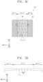
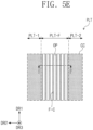
- FIG. 5A is a cross-sectional view of the display device DD according to an embodiment of the present disclosure.
- FIG. 5B is a plan view of a support plate PLT according to an embodiment of the present disclosure.
- FIG. 5C is an enlarged plan view of a portion of the support plate PLT shown in FIG. 5B .
- FIG. 5D is a cross-sectional view corresponding to the line I-I' of FIG. 5C .
- FIG. 5E is an enlarged plan view of a portion of the support plate PLT shown in FIG. 5B .
- FIG. 5A shows an unfolded state in which the display module DM is not folded.
- regions for distinguishing the display module DM are shown on the basis of the display panel DP of FIG. 3 .
- the display device DD includes a window WM, an upper member UM, the display module DM, and a lower member LM.
- Components disposed between the window WM and the display module DM is integrally referred to as the upper member UM, and components disposed at (e.g., in or on) a lower side of the display module DM are integrally referred to as the lower member LM.
- the window WM may include a thin-film glass substrate UTG, a window protection layer PF disposed on the thin-film glass substrate UTG, and a bezel pattern BP disposed on a bottom surface of the window protection layer PF.
- the window protection layer PF may include a synthetic resin film.
- the window WM may include an adhesive layer AL1 (hereinafter, referred to as a first adhesive layer) configured to bond the window protection layer PF and the thin-film glass substrate UTG to each other.
- the bezel pattern BP overlaps with the non-display area NDA shown in FIG. 1A .
- the bezel pattern BP may be disposed on one surface of the thin-film glass substrate UTG, or of the window protection layer PF.
- FIG. 5A illustrates an example of the bezel pattern BP disposed on the bottom surface of the window protection layer PF.
- the present disclosure is not limited thereto, and the bezel pattern BP may be disposed on a top surface of the window protection layer PF.
- the bezel pattern BP may be provided as a colored shielding film, for example, in a coating manner.
- the bezel pattern BP may include a base material, and a dye or pigment mixed with the base material.
- a thickness of the thin-film glass substrate UTG may be about 15 ⁇ m to about 45 ⁇ m.
- the thin-film glass substrate UTG may be chemical strengthening glass.
- the thin-film glass substrate UTG may minimize or reduce the generation of a fold, even when folding and unfolding are repeated.
- a thickness of the window protection layer PF may be about 50 ⁇ m to about 80 ⁇ m.
- the synthetic resin film of the window protection layer PF may include Polyimide, Polycarbonate, Polyamide, Triacetylcellulose, Polymethylmethacrylate, or Polyethylene terephthalate.
- at least one of a hard coating layer, an anti-fingerprint layer, or an anti-reflection layer may be disposed on the top surface of the window protection layer PF.
- the first adhesive layer AL1 may be provided with a Pressure Sensitive Adhesive (PSA) film, or an Optically Clear Adhesive (OCA).
- PSA Pressure Sensitive Adhesive
- OCA Optically Clear Adhesive
- the adhesive layers described below may also include the same type of adhesive as that of the first adhesive layer AL1.
- the first adhesive layer AL1 may be separated from the thin-film glass substrate UTG.
- the window protection layer PF may have a lower strength than that of the thin-film glass substrate UTG, and thus, may be relatively easily scratched. After the first adhesive layer AL1 is separated from the window protection layer PF, a new window protection layer PF may be adhered to the thin-film glass substrate UTG.
- the upper member UM includes a top film UL.
- the top film UL may include a synthetic resin film.
- the synthetic resin film may include Polyimide, Polycarbonate, Polyamide, Triacetylcellulose, Polymethylmethacrylate, or Polyethylene terephthalate.
- the top film UL may absorb an external impact applied to the front surface of the display device DD.
- the display module DM described above with reference to FIG. 4 may include the anti-reflection layer ARL that replaces the polarization film, and thus, a front impact strength of the display device DD may be reduced.
- the top film UL may compensate for the reduced impact strength by employing the anti-reflection layer ARL.
- the top film UL may be omitted as needed or desired.
- the upper member UM may include a second adhesive layer AL2 configured to bond the top film UL and the window WM to each other, and a third adhesive layer AL3 configured to bond the top film UL and the display module DM to each other.
- the lower member LM may include a panel protection layer PPL, a barrier layer BRL, a support plate PLT, a cover layer SCV, a digitizer DTM, and fourth to eighth adhesive layers AL4 to AL8.
- some of the foregoing components may be omitted as needed or desired.
- the barrier layer BRL, the cover layer SCV, or the digitizer DTM, and the adhesive layers related thereto may be omitted as needed or desired.
- the panel protection layer PPL may be disposed under (e.g., underneath) the display module DM.
- the panel protection layer PPL may protect the bottom (e.g., the rear) of the display panel DM.
- the panel protection layer PPL may include a flexible synthetic resin film.
- the panel protection layer PPL may include polyethylene terephthalate.
- the panel protection layer PPL may not be disposed at (e.g., in or on) the bending area BA.
- the panel protection layer PPL may include a first panel protection layer PPL-1 configured to protect the first area AA1, and a second panel protection layer PPL-2 configured to protect the second area AA2.
- the fourth adhesive layer AL4 bonds the panel protection layer PPL and the display panel DP to each other.
- the fourth adhesive layer AL4 may include a first portion AL4-1 corresponding to the first panel protection layer PPL-1, and a second portion AL4-2 corresponding to the second panel protection layer PPL-2.
- the second panel protection layer PPL-2 may be disposed under (e.g., underneath) the first area AA1 and the first panel protection layer PPL-1, together with the second area AA2. Because the panel protection layer PPL is not disposed at (e.g., in or on) the bending area BA, the bending area BA may be more easily bent.
- the fifth adhesive layer AL5 bonds the panel protection layer PPL and the barrier layer BRL to each other.
- the barrier layer BRL may be disposed under (e.g., underneath) the panel protection layer PPL.
- the barrier layer BRL may increase a resistance force to a compressive force according to external compression. Accordingly, the barrier layer BRL may serve to block the display panel DP from being modified.
- the barrier layer BRL may include a flexible plastic material, such as Polyimide or Polyethylene terephthalate.
- the barrier layer BRL may be a colored film, the light transmittance thereof which is low.
- the barrier layer BRL may absorb light incident externally.
- the barrier layer BRL may be a black synthetic resin.
- the sixth adhesive layer AL6 bonds the barrier layer BRL and the support plate PLT to each other.
- the sixth adhesive layer AL6 may include a first portion AL6-1 and a second portion AL6-2 that are spaced apart from each other.
- a distance D6 (or interval) between the first portion AL6-1 and the second portion AL6-2 corresponds to a width of the folding area FA0, and may be larger than a gap GP that will be described in more detail below.
- the support plate PLT is disposed under (e.g., underneath) the barrier layer BRL.
- the support plate PLT supports components disposed at (e.g., in or on) an upper side of the support plate PLT, and maintains or substantially maintains an unfolded state and a folded state of the display device DD.
- the support plate PLT may have a larger strength than that of the barrier layer BRL.
- the support plate PLT may include a metal material having a higher strength.
- the support plate PLT may include a substance having an elastic modulus of 60 GPa or higher.
- the support plate PLT may include a metal substance, such as stainless steel.
- the support plate PLT may also include a fiber-reinforced composite.
- the support plate PLT may include a reinforced fiber disposed inside a matrix unit.
- the reinforced fiber may be carbon fiber, or glass fiber.
- the matrix unit may include a polymer resin.
- the matrix unit may include a thermoplastic resin.
- the matrix unit may include a polyamide-based resin or a polypropylene-based resin.
- the fiber-reinforced composite may be carbon fiber-reinforced plastic (CFRP) or glass fiber-reinforced plastic (GFRP).
- the support plate PLT may include at least a first support part PLT-1 corresponding to the first non-folding area NFA10, and a second support part PLT-2 corresponding to the second non-folding area NFA20.
- the support plate PLT may include a folding part PLT-F that corresponds to the folding area FA0, and is disposed between the first support part PLT-1 and the second support part PLT-2.
- a plurality of openings OP are defined in the folding part PLT-F.
- the first support part PLT-1, the second support part PLT-2, and the folding part PLT-F may have an integrated shape.
- the shape of the folding part PLT-F changes as the electronic device ED changes from a first mode to a second mode, but the shapes of the first support part PLT-1 and the second support part PLT-2 are not changed.
- Each of the first support part PLT-1 and the second support part PLT-2 provides a planar support surface, regardless of an operation mode.
- the first support part PLT-1 and the second support part PLT-2 may be defined as a first area in which the shapes thereof are not changed according to a change in the operation mode of the electronic device ED.
- the folding part PLT-F may be defined as a second area in which the shape thereof is changed according to the operation mode change of the electronic device ED.
- the plurality of openings OP may be arrayed, so that the folding area FA0 has a lattice shape in a plan view.
- the flexibility of the folding part PLT-F is improved by the plurality of openings OP.
- the folding part PLT-F may prevent or substantially prevent foreign matter from being permeated from the first support part PLT-1 and the second support part PLT-2 to an open center area of the barrier layer BRL.
- the flexibility of the folding part PLT-F is improved by the plurality of openings OP.
- the plurality of openings OP are defined in the folding part PLT-F.
- An area other than the plurality of openings OP is defined as a support area.
- the support area may include first extension parts F-C and second extension parts F-L.
- Each of the first extension parts F-C extends in the first direction DR1, and the first extension parts F-C are arrayed along the second direction DR2.
- Each of the second extension parts F-L extends in the second direction DR2, and is disposed between adjacent first extension parts F-C.
- the first extension parts F-C and the second extension parts F-L may define a lattice shape.
- the first extension parts F-C may be positioned, so that the plurality of openings OP are disposed in a zig-zag manner along the second direction DR2.
- each of the plurality of openings OP may have a uniform or substantially uniform width.
- the width of each of the plurality of openings OP may not change in the third direction DR3, and may have a constant or substantially constant value.
- each of the first extension parts F-C may correspond to a stick member (e.g., a stick shape) extending in the first direction DR1.
- the stick members may be arrayed between the first support part PLT-1 and the second support part PLT-2 at a uniform or substantially uniform interval along the second direction DR2.
- a length of the stick members may be the same or substantially the same as the length of the first support part PLT-1 or the second support part PLT-2 in the first direction DR1. Areas between the stick members may correspond to the openings OP.
- the cover layer SCV and the digitizer DTM may be disposed under (e.g., underneath) the support plate PLT.
- the cover layer SCV is disposed to overlap with the folding area FA0.
- the digitizer DTM may include a first digitizer DTM-1 and a second digitizer DTM-2 overlapping with the first support part PLT-1 and the second support part PLT-2, respectively.
- a portion of each of the first digitizer DTM-1 and the second digitizer DTM-2 may be disposed under (e.g., underneath) the cover layer SCV.
- the seventh adhesive layer AL7 bonds the support plate PLT and the digitizer DTM to each other, and the eighth adhesive layer AL8 bonds the cover layer SCV and the support plate PLT to each other.
- the seventh adhesive layer AL7 may include a first part AL7-1 configured to bond the first support part PLT-1 and the first digitizer DTM-1 to each other, and a second part AL7-2 configured to bond the second support part PLT-2 and the second digitizer DTM-2 to each other.
- the cover layer SCV may be disposed between the first part AL7-1 and the second part AL7-2 in the second direction DR2.
- the cover layer SCV may be spaced apart from the digitizer DTM to prevent or substantially prevent interference to the digitizer DTM in an unfolded state.
- a sum of the thicknesses of the cover layer SCV and the eighth adhesive layer AL8 may be smaller than a thickness of the seventh adhesive layer AL7.
- the cover layer SCV may cover the openings OP of the folding part PLT-F.
- the cover layer SCV may have a lower elastic modulus than that of the support plate PLT.
- the cover layer SCV may include thermoplastic polyurethane, rubber, or silicone, but the present disclosure is not limited thereto.
- the digitizer DTM may be referred to as an EMR sensing panel, and includes a plurality of loop coils configured to generate a magnetic field of a suitable resonance frequency (e.g., a predetermined or preset resonance frequency) with an electronic pen.
- the magnetic field provided by the loop coils is applied to an LC resonance circuit configured from an inductor (coil) and a capacitor of the electronic pen.
- the coils generate a current by means of the received magnetic field, and deliver the generated current to the capacitor. Accordingly, the capacitor is charged with the current input from the coils, and the charge current is discharged to the coils. Then, the magnetic field of the resonance frequency is emitted to the coils.
- the magnetic field emitted by the electronic pen may be absorbed again by the loop coils of the digitizer, and accordingly, it may be determined at which position on a touch screen that the electronic pen is located.
- the first digitizer DTM-1 and the second digitizer DTM-2 are spaced apart from each other with the gap (e.g., the predetermined or prescribed gap) GP defined therebetween.
- the gap GP may be about 0.3 mm to 3 mm, and may be disposed to correspond to the folding area FA0.
- FIG. 6A is an equivalent circuit diagram of a pixel PXij according to an embodiment of the present disclosure.
- FIG. 6B is a timing diagram illustrating a pixel driving method according to an embodiment of the present disclosure.
- FIG. 6A illustrates an example of a pixel PXij connected to an i-th scan line SLi and a j-th data line DLj of a first group, where i and j are natural numbers.
- the pixel PXij may include a pixel driving circuit PC (hereinafter, referred to as a pixel circuit) and a light emitting element LD.
- the pixel circuit PC may include first to seventh transistors T1 to T7, and a capacitor Cst.
- the first transistor T1, the second transistor T2, and the fifth transistor T5 to the seventh transistor T7 are P-type transistors
- the third transistor T3 and the fourth transistor T4 are N-type transistors.
- each of the first to seventh transistors T1 to T7 may be implemented with any suitable one of a P-type transistor or an N-type transistor.
- An input area (e.g., an input electrode) of the N-type transistor is described as a drain (e.g., a drain area), and an input area of the P-type transistor is described as a source (e.g., a source area).
- An output area (e.g., an output electrode) of the N-type transistor is described as a source (e.g., a source area), and an output area of the P-type transistor is described as a drain (e.g., a drain area).
- at least one of the first to seventh transistors T1 to T7 may be omitted as needed or desired.
- the first transistor T1 may be a driving transistor
- the second transistor T2 may be a switching transistor.
- the capacitor Cst is electrically connected between a reference node RN and a power line PL through which the first power supply voltage ELVDD is received.
- the capacitor Cst includes a first electrode CE10 electrically connected to the reference node RN, and a second electrode CE20 electrically connected to the power line PL.
- the light emitting element LD is electrically connected between the first transistor T1 and a signal line SL.
- the signal line SL may provide a second power supply voltage ELVSS or a driving signal TDS to a cathode of the light emitting element LD.
- the second power supply voltage ELVSS may have a lower level than that of the first power supply voltage ELVDD.
- the first transistor T1 is electrically connected between the power line PL and an anode of the light emitting element LD.
- a source S1 of the first transistor T1 is electrically connected to the power line PL.
- electrically connected between a transistor and a signal line or between a transistor and another transistor means that "a source, a drain, and a gate of the transistor have an integrated shape with the signal line or are connected through connection electrodes".
- Another transistor may be disposed or may not be disposed between the source S1 of the first transistor T1 and the power line PL.
- the drain D1 of the first transistor T1 is electrically connected to the anode of the light emitting element LD.
- Another transistor may be disposed or may not be disposed between the drain D1 of the first transistor T1 and the anode of the light emitting element LD.
- a gate G1 of the first transistor T1 is electrically connected to the reference node RN.
- the second transistor T2 is electrically connected between a j-th data line DLj and the source S1 of the first transistor T1.
- the source S2 of the second transistor T2 is electrically connected to the j-th data line DLj
- a drain D2 of the second transistor T2 is electrically connected to the source S1 of the first transistor T1.
- the gate G2 of the second transistor T2 may be electrically connected to an i-th scan line SLi of the first group.
- the third transistor T3 is electrically connected between the reference node RN and the drain D1 of the first transistor T1.
- a drain D3 of the third transistor T3 is electrically connected to the drain D1 of the first transistor T1, and a source S3 of the third transistor T3 is electrically connected to the reference node RN.
- the third transistor T3 is illustrated as having a single gate, but in some embodiments, the third transistor T3 may include a plurality of gates. In the present embodiment, a gate G3 of the third transistor T3 may be electrically connected to an i-th scan line GLi of a second group.
- the fourth transistor T4 is electrically connected between the reference node RN and a first voltage line VL1.
- a drain D4 of the fourth transistor T4 is electrically connected to the reference node RN, and a source S4 of the fourth transistor T4 is electrically connected to the first voltage line VL1.
- the fourth transistor T4 is illustrated as having a single gate, but in some embodiments, the fourth transistor T4 may include a plurality of gates. In the present embodiment, a gate G4 of the fourth transistor T4 may be electrically connected to an i-th scan line HLi of a third group.
- the fifth transistor T5 is electrically connected between the power line PL and the source S1 of the first transistor T1.
- a source S5 of the fifth transistor T5 is electrically connected to the power line PL, and a drain D5 of the fifth transistor T5 is electrically connected to the source S1 of the first transistor T1.
- a gate of the fifth transistor T5 may be electrically connected to the i-th emission line ELi.
- the sixth transistor T6 is electrically connected between the light emitting element LD and the drain D1 of the first transistor T1.
- a source S6 of the sixth transistor T6 is electrically connected to the drain D1 of the first transistor T1, and a drain D6 of the sixth transistor T6 is electrically connected to the anode of the light emitting element LD.
- a gate G6 of the sixth transistor T6 may be electrically connected to the i-th emission line ELi. In an embodiment of the present disclosure, the gate G6 of the sixth transistor T6 may be connected to a signal line different from that of the gate G5 of the fifth transistor T5.
- the seventh transistor T7 is electrically connected between the second voltage line VL2 and the drain D6 of the sixth transistor T6.
- a source S7 of the seventh transistor T7 is electrically connected to the drain D6 of the sixth transistor T6, and a drain D7 of the seventh transistor T7 is electrically connected to the second voltage line VL2.
- a gate G7 of the seventh transistor T7 may be electrically connected to an (i+1)-th scan line SLi+1 of the first group.
- each of signals EMi, GIi, GWi, GCi, and GWi+1 may have a high level V-HIGH during a partial period, and a low level V-LOW during a partial period.
- Some of the signals EMi, GIi, GWi, GCi, and GWi+1 are illustrated as having the same or substantially the same pulse width as each other in FIG. 6B , but the present disclosure is not limited thereto.
- Each of the pulse widths of the signals EMi, GIi, GWi, GCi, and GWi+1 may be determined in consideration of a target turn-on period of each of the first to seventh transistors T1 to T7.
- the N-type transistors are turned on when corresponding signals have the high levels V-HIGH, and the P-type transistors are turned on when corresponding signals have the low levels V-LOW.
- the emission control signal EMi has the high level V-HIGH
- the fifth transistor T5 and the sixth transistor T6 are turned off.
- a current path is not provided between the power line PL and the light emitting element LD. Accordingly, a corresponding period may be defined as a non-light emission period.
- the fourth transistor T4 When a scan signal Gli is applied to the i-th scan line HLi of the third group, the fourth transistor T4 is turned on. When the fourth transistor T4 is turned on, the reference node RN is initialized by a first initialization voltage Vint.
- the second transistor T2 and the third transistor T3 are turned on.
- the first transistor T1 is turned on.
- a voltage corresponding to a data signal Dj (e.g., see FIG. 6A ) is provided to the reference node RN.
- the capacitor Cst stores the voltage corresponding to the data signal Dj.
- the voltage corresponding to the data signal Dj may be a voltage obtained by subtracting a threshold voltage Vth of the first transistor T1 from the data signal Dj.
- the seventh transistor T7 When a scan signal GWi+1 applied to an (i+1)-th scan line SLi+1 of the first group has the low level V-LOW, the seventh transistor T7 is turned on. As the seventh transistor T7 is turned on, the anode of the light emitting element LD is initialized to a second initialization voltage VAint. A parasite capacitor of the light emitting element LD may be discharged.
- the emission control signal EMi has the low level V-LOW
- the fifth transistor T5 and the sixth transistor T6 are turned on.
- the fifth transistor T5 is turned on
- the first power supply voltage ELVDD is provided to the first transistor T1.
- the sixth transistor T6 is turned on, the first transistor T1 is electrically connected to the light emitting element LD.
- the light emitting element LD generates light having a luminance corresponding to the received current amount.
- FIG. 7A is an enlarged plan view of the first display area DA1 according to an embodiment of the present disclosure.
- FIG. 7A is an enlarged plan view of the portion AA of the first display area DA1 (e.g., see FIG. 3 ) according to an embodiment of the present disclosure.
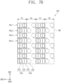
- FIG. 7B is an enlarged plan view of the second display area DA2 according to an embodiment of the present disclosure.
- FIG. 7B is an enlarged plan view of the portion BB of the second display area DA2 (e.g., see FIG. 3 ) according to an embodiment of the present disclosure.
- FIG. 7C is a plan view of the second display area DA2 overlapping with the support plate PLT.
- a resolution of a display device may be determined by the number of pixels disposed in a reference area, and may be measured in, for example, pixels per inch (PPI).
- PPI pixels per inch
- the resolution of a light emitting element and the resolution of a pixel circuit are the same as the resolution of a pixel. This is because each of the pixels includes a light emitting element and the pixel circuit that are connected one to one, and the light emitting elements and the pixel circuits are disposed uniformly at (e.g., in or on) the entire display area DP-DA (e.g., see FIG. 3 ).
- the first display area DA1 and the second display area DA2 may have different dispositions of the pixels PX.
- the first display area DA1 and the second display area DA2 have the same or substantially the same disposition of the light emitting elements LD as each other, but have different dispositions of the pixel circuits PC from each other.
- the same disposition of the light emitting elements may mean that an interval between the light emitting elements is the same or substantially the same.
- color arrays of the light emitting elements are the same or substantially the same.
- first pixels PX1 are disposed at (e.g., in or on) the first display area DA1.
- the first pixels PX1 are uniformly or substantially uniformly disposed at (e.g., in or on) the first display area DA1.
- Each of the first pixels PX1 includes a light emitting element LD1 (hereinafter, referred to as a first light emitting element), and a pixel circuit PC1 (hereinafter, referred to as a first pixel circuit) electrically connected to the first light emitting element LD1.
- the first light emitting element LD1 may include a red light emitting element, a green light emitting element, and a blue light emitting element.
- FIG. 7A illustrates an anode as a representative of the first light emitting element LD1, or in other words, an anode of the red light emitting element, an anode of the green light emitting element, and an anode of the blue light emitting element.
- the first pixel circuit PC1 corresponding to the anode may be connected to each other through a contact hole. This will be described in more detail below.
- the anode is illustrated as circular in the figures, but the shape of the anode is not particularly limited thereto.
- first pixel circuits PC1 are disposed adjacent to each other to provide one circuit group.
- a plurality of circuit groups are disposed and spaced apart from each other at a suitable interval (e.g., a predetermined or certain interval).
- a suitable interval e.g., a predetermined or certain interval.
- the first pixel circuits PC1 may be disposed and spaced apart from each other in rows of pixels PXL1 to PXL4 at a uniform or substantially uniform interval.
- the first pixel circuit PC1 may have the equivalent circuit shown in FIG. 6A .
- An area shown as the first pixel circuit PC1 in FIG. 7A represents an area occupied by the first to seventh transistors T1 to T7 and the capacitor Cst shown in FIG. 6A .
- the first pixel circuits PC1 are illustrated as having the same or substantially the same shape as each other, but the present disclosure is not limited thereto.
- the first pixel circuit PC1 may include a first type pixel circuit and a second type pixel circuit that are paired with each other and repeatedly disposed.
- the plurality of rows of pixels PXL1 to PXL4 may be defined at (e.g., in or on) the first display area DA1.
- green light emitting elements are arrayed along the second direction DR2
- red light emitting elements and blue light emitting elements are alternately arrayed along the second direction DR2.
- blue light emitting elements and red light emitting elements are alternately arrayed along the second direction DR2.
- first pixel row PXL1 and the second pixel row PXL2 may include the same arrays of the light emitting elements as each other.
- Each of the first pixel row PXL1 and the second pixel row PXL2 may include a plurality of pixel units arrayed in the second direction DR2.
- Each of the plurality of pixel units may include a red light emitting element, a green light emitting element, or a blue light emitting element arranged along the second direction DR2.
- Each of the pixel units may further include a fourth color light emitting element configured to generate a colored light different from those generated from the red, green, and blue light emitting elements.
- the second display area DA2 includes first partial areas P1 and second partial areas P2.
- the first partial areas P1 and the second partial areas P2 may be alternately arranged along the second direction DR2.
- the first partial area P1 may overlap with the first extension part F-C shown in FIG. 5C
- the second partial area P2 may overlap with the opening OP shown in FIG. 5C .
- light emitting elements LD2 and LD3 of the pixel rows PXL1 to PXL4 are illustrated as overlapping with the support plate PLT.
- FIG. 7C light emitting elements LD2 and LD3 of the pixel rows PXL1 to PXL4 are illustrated as overlapping with the support plate PLT.
- the light emitting elements LD2 and LD3 are illustrated to be in a partial area BB, but in another area, second pixels PX2 and third pixels PX3 may be disposed according to a suitable rule, which will be described in more detail below.
- the second pixels PX2 and the third pixels PX3 are disposed at (e.g., in or on) the second display area DA2.
- Each of the second pixels PX2 includes a light emitting element LD2 (hereinafter, a second light emitting element), and a pixel circuit PC2 (hereinafter, in connection with the figures, referred to as a second pixel circuit) electrically connected to the second light emitting element LD2.
- Each of the third pixels PX3 includes a light emitting element LD3 (hereinafter, referred to as a third light emitting element), and a pixel circuit PC3 (hereinafter, in connection with the figures, referred to as a third pixel circuit) electrically connected to the third light emitting element LD3.
- a light emitting element LD3 hereinafter, referred to as a third light emitting element
- a pixel circuit PC3 hereinafter, in connection with the figures, referred to as a third pixel circuit
- the second light emitting element LD2 may be referred to as a first light emitting element and the third light emitting element LD3 may be referred to as a second light emitting element.
- the first pixel circuit PC1 may be referred to as a third pixel circuit and the first light emitting element LD1 may be referred to as a third light emitting element in the claims and above general part of the description.
- the second pixel circuits PC2 and the third pixel circuits PC3 are arrayed according to a different rule from that of the first pixel circuits PC1.
- the resolution of the pixel circuits PC1 in the first display area DA1 may be different from those of the pixel circuits PC2 and PC3 in the second display area DA2.
- the resolution of the first pixel circuits PC1 in the first display area DA1 may be different from that of the pixel circuits in the first partial area P1 and that of the pixel circuits in the second partial area P2.
- the resolution of the pixel circuits in the first partial area P1 may be different from that of the pixel circuits in the second partial area P2.
- the resolutions of the pixels PX in the first display area DA1 and the second display area DA2 are the same or substantially the same as each other, and the resolutions of the light emitting elements in the first display area DA1 and the second display area DA2 are the same or substantially the same as each other.
- the resolution of the pixel circuits in the first partial area P1 is higher than that of the pixel circuits in the first display area DA1.
- the pixel circuits at (e.g., in or on) the first display area DA1 are less densely disposed than those at (e.g., in or on) the first partial area P1.
- the second pixel circuits PC2 and the third pixel circuits PC3 may be disposed at (e.g., in or on) the first partial area P1.
- the second light emitting elements LD2 may overlap with the second pixel circuits PC2, but the third light emitting elements LD3 may not overlap with the third pixel circuits PC3.
- Pixel circuits may not be disposed at (e.g., in or on) the second partial area P2.
- the second partial area P2 overlapping with the openings OP of FIG. 5C has low impact resistance, and thus, short-circuit or disconnection in the circuits may occur due to an external impact.
- a fault in the pixel circuit may be reduced by minimizing or substantially minimizing the pixel circuits disposed at (e.g., in or on) the second partial area P2.
- the resolution of the pixel circuits PC2 and PC3 at (e.g., in or on) the first partial area P1 is higher in comparison with the resolution of the pixel circuits PC1 at (e.g., in or on) the first display area DA1.
- the area occupied by a single first pixel circuit PC1, the area occupied by a single second pixel circuit PC2, and the area occupied by a single third pixel circuit PC3 may be the same or substantially the same as each other.
- That the areas of the pixel circuits are the same or substantially the same as each other means that the layouts of the pixel circuits are the same or substantially the same as each other, and the sizes and array rules of the transistors providing the pixel circuits are the same or substantially the same as each other.
- the first pixel circuit PC1, the second pixel circuit PC2, and the third pixel circuit PC3 have the same or substantially the same areas as each other, and thus, uniform or substantially uniform circuits may be designed.
- Noise factors, such as peripheral signals or parasitic capacitances, which may influence the operations of the first pixel circuit PC1, the second pixel circuit PC2, and the third pixel circuit PC3, may be the same or substantially the same, and thus, the pixel circuits may be easily controlled.
- the third pixel circuit PC3 of the display panel DP may be disposed at (e.g., in or on) the first partial area P1.
- a width of the first partial area P1 is defined as W1
- a width of the second partial area P2 is defined as W2
- a standard width of the first pixel circuit PC1 which is calculated on the basis of the resolution of the pixel circuits of the first display area DA1
- H a standard width of the second pixel circuit PC2 or the third pixel circuit PC3, which is calculated on the basis of the resolution of the pixel circuits of the first partial area P1
- Z a standard widths of the second pixel circuit PC2 and the third pixel circuit PC3 are assumed to be same or substantially the same as each other.
- a standard width of the first pixel circuit PC1 means a maximum width in which the first pixel circuit PC1 may be disposed under a condition that the resolution of the first pixel circuit PC1 is satisfied.
- a standard width of the second pixel circuit PC2 or the third pixel circuit PC3 means a maximum width in which the second pixel circuit PC2 and the third pixel circuit PC3 are disposed under a condition that the resolutions of the second pixel circuit PC2 and the third pixel circuit PC3 are satisfied.
- the standard width of the first pixel circuit PC1 may be different from an actual measurement width of the first pixel circuit PC1, and the standard width of the second pixel circuit PC2 may be different from an actual measurement width of the second pixel circuit PC2.
- the standard width H of the first pixel circuit PC1 is about 78 ⁇ m.
- the standard width Z of the second pixel circuit PC2 is about 50 ⁇ m.
- the actual measurement width of the first pixel circuit PC1 may be designed to be smaller than about 78 ⁇ m, and an actual measurement width of the third pixel circuit PC3 may be smaller than about 50 ⁇ m.
- the first pixel circuit PC1 is designed to have an actual measurement width smaller than the standard width H.
- the second pixel circuit PC2 and the third pixel circuit PC3 are designed to have the same or substantially the same actual measurement width as the standard width Z.
- an area of the second display area DA2 which overlaps with the second extension part F-L shown FIG 5C , is not shown.
- the area of the second display area DA2 that overlaps with the second extension part F-L shown in FIG. 5C may have the same or substantially the same pixel structure as that of the first partial area P1, the same or substantially the same pixel structure as that of the second partial area P2, or the same or substantially the same pixel structure as that of the first display area DA1 shown in FIG. 7A , but is not particularly limited thereto.
- the third pixel circuit PC3 disposed in the area overlapping with the second extension part F-L may also be electrically connected to the third light emitting element LD3 disposed at (e.g., in or on) the second partial area P2.
- the third pixel circuit LD3 disposed in the area at (e.g., in or on) the second display area DA2, which overlaps with the second extension part F-L, may also be electrically connected to the third pixel circuit PC3 disposed at (e.g., in or on) the first partial area P1.
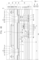
- FIG. 8A is a cross-sectional view of the first display area DA1 according to an embodiment of the present disclosure.
- FIGS. 8B and 8C are cross-sectional views of the second display area DA2 according to one or more embodiments of the present disclosure.
- FIG. 8A a silicon transistor S-TFT and an oxide transistor O-TFT of the first pixel circuit PC1, and the first light emitting element LD1 are illustrated.
- the third and fourth transistors T3 and T4 may be oxide transistors O-TFT, and the other remaining transistors may be silicon transistors S-TFT.
- FIG. 8B and FIG. 8C a portion of the second light emitting element LD2 and the second pixel circuit PC2, and a portion of the third light emitting element LD3 and the third pixel circuit PC3 are illustrated.
- the silicon transistor S-TFT shown in FIG. 8B may be the sixth transistor T6 shown in FIG. 6A .
- a barrier layer 10br may be disposed on the base layer 110.
- the barrier layer 10br prevents or substantially prevents foreign matter from entering from the outside.
- the barrier layer 10br may include at least one inorganic layer.
- the barrier layer 10br may include a silicon oxide layer and a silicon nitride layer. Each of of the silicon oxide layer and the silicon nitride layer may be provided in a plurality, and the silicon oxide layers and the silicon nitride layers may be alternately laminated.
- a first shield electrode BMLa may be disposed on the barrier layer 10br.
- the first shield electrode BMLa may include a metal.
- the first shield electrode BMLa may include molybdenum (Mo) having a good thermal resistance, an alloy containing molybdenum, titanium (Ti), or an alloy containing titanium.
- the first shield electrode BMLa may receive a bias voltage.
- the first shield electrode BMLa may also receive the first power supply voltage ELVDD.
- the first shield electrode BMLa may shield an electric potential caused by a polarization phenomenon from influencing the silicon transistor S-TFT.
- the first shield electrode BMLa may shield external light from reaching the silicon transistor S-TFT.
- the first shield electrode BMLa may be a floating electrode that is electrically isolated from another electrode or wiring.
- a buffer layer 10bf may be disposed on the barrier layer 10br.
- the buffer layer 10bf may prevent or substantially prevent a phenomenon in which metal atoms or impurities diffuse to a first semiconductor pattern SC1.
- the buffer layer 10bf may include at least one inorganic layer.
- the buffer layer 10bf may include a silicon oxide layer and/or a silicon nitride layer.
- the first semiconductor pattern SC1 may be disposed on the buffer layer 10bf.
- the first semiconductor pattern SC1 may include a silicon semiconductor.
- the silicon semiconductor may include amorphous silicon, polycrystalline, or the like.
- the first semiconductor pattern SC1 may include low temperature polysilicon.
- FIG. 8A illustrates only a portion of the first semiconductor pattern SC1, and the first semiconductor pattern SC1 may be further disposed at (e.g., in or on) another area.
- the first semiconductor pattern SC1 may be arrayed in a suitable rule (e.g., a predetermined or specific rule) across the pixels PX.
- the first semiconductor pattern SC1 may have different electrical properties according to whether or not it is doped.
- the first semiconductor pattern SC1 may include a first area having a high conductivity, and a second area having a low conductivity.
- the first area may be doped with an N-type dopant or a P-type dopant.
- a P-type transistor includes a doping area doped with a P-type dopant
- an N-type transistor includes a doping area doped with an N-type dopant.
- the second area may be a non-doping area, or may be doped at a lower concentration relative to the first area.
- the first area may have a higher conductivity than the second area, and may serve or substantially serve as an electrode or a signal line.
- the second area may correspond to or substantially correspond to a channel area (e.g., an active area) of the transistor.
- a portion of the first semiconductor pattern SC1 may be a channel of the transistor, another portion may be the source or drain of the transistor, and still another portion may be a connection electrode or a signal connection line.
- a source area SE1, a channel area AC1 (e.g., an active area), and a drain area DE1 of the silicon transistor S-TFT may be provided from the first semiconductor pattern SC1.
- the source area SE1 and the drain area DE1 may extend from the channel area AC1 in opposite directions from each other.
- the first insulation layer 10 may be disposed on the buffer layer 10bf.
- the first insulation layer 10 may cover the first semiconductor pattern SC1.
- the first insulation layer 10 may be an inorganic layer.
- the first insulation layer 10 may be a silicon oxide layer of a single layer.
- the first insulation layer 10 may also have a multi-layered structure.
- the inorganic layer of the circuit layer 120 described in more detail below may have a single layer structure or a multi-layered structure, and may include at least one of the foregoing materials, but the present disclosure is not limited thereto.
- a gate GT1 of the silicon transistor S-TFT is disposed on the first insulation layer 10.
- the gate GT1 may be a portion of a metal pattern.
- the gate GT1 overlaps with the channel area AC1.
- the gate GT1 may be used as a mask in a process for doping the first semiconductor pattern SC1.
- a first electrode CE10 of the storage capacitor Cst is disposed on the first insulation layer 10. Unlike the example shown in FIG. 8A , the first electrode CE10 may have an integrated shape with the gate GT1.
- the second insulation layer 20 may be disposed on the first insulation layer 10, and may cover the gate GT1. Although not shown in the drawing, a top electrode, which overlaps with the gate GT1, may be disposed on the second insulation layer 20. A second electrode CE20, which overlaps with the first electrode CE10, may be disposed on the second insulation layer 20.
- a second shield electrode BMLb is disposed on the second insulation layer 20.
- the second shield electrode BMLb may be disposed corresponding to a bottom of the oxide transistor O-TFT.
- the second shield electrode BMLb may be omitted as needed or desired.
- the first shield electrode BMLa may extend to the bottom of the oxide transistor O-TFT to replace the second shield electrode BMLb.
- a third insulation layer 30 may be disposed on the second insulation layer 20.
- a second semiconductor pattern SC2 may be disposed on the third insulation layer 30.
- the second semiconductor pattern SC2 may include a channel area AC2 of the oxide transistor O-TFT.
- the second semiconductor pattern SC2 may include an oxide semiconductor.
- the second semiconductor pattern SC2 may include at least one of In2O3, IGZO, ZnO, ZnSnO(ZTO) or InZnO(IZO).
- the oxide semiconductor may include a plurality of zones divided according to whether or not a TCO is reduced.
- a zone hereinafter, referred to as a reduction zone
- the reduction zone may serve or substantially serve as a source/drain or a signal line of the transistor.
- the non-reduction zone corresponds to or substantially corresponds to a semiconductor area (e.g., a channel) of the transistor.
- a portion of the second semiconductor pattern SC2 may be a semiconductor area of the transistor, another portion may be a source/drain of the transistor, and still another portion may be a signal transfer area.
- a fourth insulation layer 40 may be disposed on the third insulation layer 30. As shown in FIG. 8A , the fourth insulation layer 40 may be an insulation pattern that overlaps with the gate GT2 of the oxide transistor O-TFT, while exposing the source area SE2 and the drain area DE2 of the oxide transistor O-TFT. In an embodiment of the present disclosure, the fourth insulation layer 40 may commonly overlap with the plurality of pixels, and may cover the second semiconductor pattern SC2.
- the gate GT2 of the oxide transistor O-TFT is disposed on the fourth insulation layer 40.
- the gate GT2 of the oxide transistor O-TFT may be a portion of a metal pattern.
- the gate GT2 of the oxide transistor O-TFT may overlap with the channel area AC2.
- a fifth insulation layer 50 may be disposed on the fourth insulation layer 40, and the fifth insulation layer 50 may cover the gate GT2.
- Each of the first to fifth insulation layers 10 to 50 may be an inorganic layer.
- a first connection electrode CNE1 may be disposed on the fifth insulation layer 50.
- the first connection electrode CNE1 may be connected to the drain area DE1 of the silicon transistor S-TFT through a contact hole penetrating through the first to fifth insulation layers 10 to 50.
- a sixth insulation layer 60 may be disposed on the fifth insulation layer 50.
- a second connection electrode CNE2 may be disposed on the sixth insulation layer 60.
- the second connection electrode CNE2 may be connected to the first connection electrode CNE1 through a contact hole penetrating through the sixth insulation layer 60.
- a data line DL may be disposed on the sixth insulation layer 60.
- a seventh insulation layer 70 may be disposed on the sixth insulation layer 60, and may cover the second connection electrode CNE2 and the data line DL.
- Each of the sixth and seventh insulation layers 60 and 70 may be an organic layer.
- the first light emitting element LD1 may include an anode AE1 (e.g., a first electrode), a light emitting layer EML1, and a cathode CE (e.g., a second electrode).
- the cathodes CE of the second and third light emitting elements LD2 and LD3 described in more detail below may have a shape integrated with the cathode CE of the first light emitting element LD1.
- the cathode CE may be commonly provided to the first to third light emitting elements LD1, LD2, and LD3.
- the anode AE1 of the first light emitting element LD1 may be disposed on the seventh insulation layer 70.
- the anode AE1 may be a (semi-) transparent electrode or a reflective electrode.
- a pixel definition layer PDL may be disposed on the seventh insulation layer 70.
- the pixel definition layer PDL may have a light absorption property, and for example, may have a black color.
- the pixel definition layer PDL may include a black coloring agent.
- the black coloring agent may include a black dye or a black pigment.
- the black coloring agent may include carbon black, a metal such as chromium, or an oxide thereof.
- the pixel definition layer PDL may correspond to a light shielding pattern having a light shielding property.
- the pixel definition layer PDL may cover a portion of the anode AE1.
- an opening PDL-OP exposing a portion of the anode AE1 may be defined in the pixel definition layer PDL.
- a hole control layer may be disposed between the anode AE1 and the light emitting layer EML1.
- the hole control layer may include a hole transport layer, and may further include a hole injection layer.
- An electron control layer may be disposed between the light emitting layer EML1 and the cathode CE.
- the electron control layer may include an electron transport layer, and may further include an electron injection layer.
- the hole control layer and the electron control layer may be commonly provided in the plurality of pixels PX (e.g., see FIG. 3 ) using an open mask.
- the encapsulation layer 140 may be disposed on the light-emitting element layer 130.
- the encapsulation layer 140 may include an inorganic layer 141, an organic layer 142, and an inorganic layer 143, which are successively laminated, but the layers providing the encapsulation layer 140 are not limited thereto.
- the inorganic layers 141 and 143 may protect the light emitting element layer 130 from moisture and/or oxygen, and the organic layer 142 may protect the light emitting element layer 130 from foreign matter, such as dust particles.
- the inorganic layers 141 and 143 may include a silicon nitride layer, a silicon oxynitride layer, a silicon oxide layer, a titanium oxide layer, an aluminum oxide layer, or the like.
- the organic layer 142 may include an acrylic-based organic layer, but the present disclosure is not limited thereto.
- the input sensor ISP may be disposed on the display panel DP.
- the input sensor ISP may include at least one conductive layer, and at least one insulation layer.
- the input sensor ISP may include a first insulation layer 210, a first conductive layer 220, a second insulation layer 230, and a second conductive layer 240.
- the first insulation layer 210 may be directly disposed on the display panel DP.
- the first insulation layer 210 may be an inorganic layer including any one of silicon nitride, silicon oxynitride, or silicon oxide.
- Each of the first sensing conductive layer 220 and the second sensing conductive layer 240 may have a single layer structure or a multi-layered structure laminated along the third direction DR3.
- Each of the first conductive layer 220 and the second conductive layer 240 may include conductive lines defining an electrode of a mesh shape.
- the conductive lines of the first conductive layer 220 and the conductive lines of the second conductive layer 240 may or may not be connected through a contact hole penetrating the second insulation layer 230. According to the type of a sensor providing the input sensor ISP, a connection relationship may be determined between the conductive lines of the first conductive layer 220 and the conductive lines of the second conductive layer 240.
- Each of the first conductive layer 220 and the second conductive layer 240 of single layer structures may include a metal layer or a transparent conductive layer.
- the metal layer may include molybdenum, silver, titanium, copper, aluminum, or an alloy thereof.
- the transparent conductive layer may include a TCO, such as indium tin oxide (ITO), indium zinc oxide (IZO), zinc oxide (ZnOx), or indium-zinc-tin oxide (IZTO).
- the transparent conductive layer may include a conductive polymer, such as PEDOT, a metal nano-wire, or graphene.
- Each of the first conductive layer 220 and the second conductive layer 240 of multi-layered structures may include a plurality of metal layers.
- the layers may have a three-layered structure of titanium/aluminum/titanium.
- the conductive layer of the multi-layered structure may include at least one metal layer, and at least one transparent conductive layer.
- the second insulation layer 230 may be disposed between the first conductive layer 220 and the second conductive layer 240.
- the anti-reflection layer ARL may be disposed on the input sensor ISP.
- the anti-reflection layer ARL may include a division layer 310, a color filter 320, and a planarization layer 330.
- a material defining the division layer 310 may be used without particular limitation, so long as the material absorbs light.
- the division layer 310 is a layer having a black color, and in an embodiment, may include a black coloring agent.
- the black coloring agent may include a black dye or a black pigment.
- the black coloring agent may include carbon black, a metal such as chromium, or an oxide thereof.
- the division layer 310 may cover the second conductive layer 240 of the input sensor ISP.
- the division layer 310 may prevent or substantially prevent reflection of external light caused by the second conductive layer 240.
- An opening 310-OP may be defined in the division layer 310.
- the opening 310-OP may overlap with the anode AE1.
- the color filter 320 may overlap with the opening 310-OP.
- the color filter 320 may contact the division layer 310.
- the planarization layer 330 may cover the division layer 310 and the color filter 320.
- the planarization layer 330 may include an organic material, and may provide a planar or substantially planar surface at (e.g., in or on) a top surface of the planarization layer 330. In an embodiment of the present disclosure, the planarization layer 330 may be omitted as needed or desired.
- the oxide transistor O-TFT of the second pixel circuit PC2 is not shown, unlike those shown of the first pixel circuit PC1 and the third pixel circuit PC3.
- redundant description of the second pixel PX2 and the third pixel PX3 that is the same or substantially the same as that of the first pixel PX1 described above with reference to FIG. 8A may not be repeated.
- the anode AE3 of the third light emitting element LD3 disposed at (e.g., in or on) the second partial area P2 may be electrically connected to the third pixel circuit PC3 disposed at (e.g., in or on) the first partial area P1.
- the anode AE3 of the third light emitting element LD3 may be electrically connected to the silicon transistor S-TFT or the oxide transistor O-TFT.
- the anode AE3 of the third light emitting element LD3 is illustrated as being connected to the silicon transistor S-TFT.
- a line part LP of the anode AE3 of the third light emitting element LD3 may extend from an electrode part EP overlapping with the opening PDL-OP.
- the line part LP may be electrically connected with the third pixel circuit PC3 through connection electrodes CNE1' and CNE2'.
- connection line TWL connecting the anode AE3 of the third light emitting element LD3 and the third pixel circuit PC3 to each other may be further disposed.
- the connection line TWL may be disposed at (e.g., in or on) a different layer from that of the anode AE3.
- the connection line TWL may be disposed between the sixth insulation layer 60 and the seventh insulation layer 70.
- the connection line TWL may be connected to the anode AE3 and the first connection electrode CNE1' through contact holes.
- the disposition of the connection line TWL may address an issue of short-circuiting with an anode of another light emitting element. This will be described in more detail below with reference to FIG. 10 .
- FIGS. 9A and 9B are enlarged plan views of the first display area DA1 according to embodiments of the present disclosure.
- FIGS. 9C and 9D are enlarged plan views of the second display area DA2 according to embodiments of the present disclosure.
- an interval SD between first pixel circuits PC1 disposed adjacent to each other are increased compared to that of the first pixel circuits PC1 shown in FIG. 7A .
- the interval SD of the first pixel circuits PC1 may be larger than that between the second and third pixel circuits PC2 and PC3 shown in FIG. 7B .
- interference between the first pixel circuits PC1 may be reduced.
- the area of the first pixel circuits PC1 are increased compared to that of the first pixel circuits PC1 shown in FIG. 7A .
- the transistors T1 to T7 e.g., see FIG. 6A
- the transistors T1 to T7 may be freely designed. Interference between the transistors T1 to T7 may be reduced by designing the transistors T1 to T7 in a wider area.
- the second display area DA2 shown in FIGS. 7B and 9C it may be understood that, when the sum of the widths of the first partial area P1 and the second partial area P2 is assumed to be constant or substantially constant, a ratio of the width of the first partial area P1 over the sum in the second display area DA2 shown in FIG. 9C increases when compared to that of the second display area DA2 shown in FIG. 7B .
- the interval between adjacent pixel circuits from among the second pixel circuits PC2 and the third pixel circuits PC3 may increase. Accordingly, interference between the adjacent pixel circuits may be reduced.
- the width of the second partial area P2 in the second display area DA2 shown in FIG. 9D is increased compared to that of the second display area DA2 shown in FIG. 7B .
- the width of the second partial area P2 may be larger than that of the first partial area P1.
- the second display area DA2 may further include a fourth pixel PX4 including a fourth pixel circuit PC4 disposed at (e.g., in or on) the second partial area P2, and a fourth light emitting element LD4 disposed at (e.g., in or on) the second partial area P2 and connected to the fourth pixel circuit PC4.
- the fourth pixel circuit PC4 is disposed at (e.g., in or on) the second partial area P2
- the resolution of the pixel circuits in the second partial area P2 is lower than those of the pixel circuits in the first display area DA1 and the pixel circuits in the first partial area P1.
- the resolution of the pixel circuits in the second partial area P2 is lowered to reduce disconnection or short-circuit of the pixel circuits that may occur in the second partial area P2.
- FIG. 10 is an enlarged plan view of the first and second display areas DA1 and DA2 according to an embodiment of the present disclosure.
- the display panel DP (e.g., see FIG. 3 ) further includes the fourth pixel PX4 including the fourth pixel circuit PC4 disposed at (e.g., in or on) the first display area DA1, and the fourth light emitting element LD4 disposed at (e.g., in or on) the second partial area P2 of the second display area DA2.
- the resolution of the pixel circuits at (e.g., in or on) the first partial area P1 excessively increases in comparison to that in the first display area DA1 by disposing the fourth pixel circuit PC4 at (e.g., in or on) the first display area DA1.
- the fourth light emitting elements LD4 may be disposed in some of or all of the plurality of second partial areas P2.
- connection line TWL which electrically connects the fourth pixel circuit PC4 and the fourth light emitting element LD4 to each other, may be the same or substantially the same as the connection line TWL described above with reference to FIG. 8C .
- the connection line TWL may overlap with the light emitting elements disposed at (e.g., in or on) an upper side.
- the display panel DP may further include the fourth pixel PX4 shown in FIG. 10 .
- the third pixel circuit PC3 may not be disposed at (e.g., in or on) the first partial area P1
- the fourth pixel circuit PC4 may be disposed at (e.g., in or on) the first display area DA1.
- the third pixel PX3 and the fourth pixel PX4 are identified according to the positions of the pixel circuits.
- a ratio of the number of the third pixels PX3 and the number of the fourth pixels PX4 may be determined in consideration of the resolution of the pixel circuits in the first partial area P1 and the width (or area) of the first partial area P1.
- the third pixel circuit PC3 disposed at (e.g., in or on) the first partial area P1, which is most adjacent to the first display area DA1, is connected with the third light emitting element LD3 through the connection line TWL.
- the connection relationship between the third pixel circuit PC3 and the third light emitting element LD3 may be provided in various suitable types, for example, as those shown in FIGS. 8B and 8C , but is not limited to a particular structure.
- FIG. 11A is an enlarged plan view of a portion of a support plate PLT according to an embodiment of the present disclosure.
- FIGS. 11B through 11E are cross-sectional views corresponding to the line II-II' of FIG. 11A .
- FIGS. 12A through 12E are cross-sectional views of the support plate PLT according to one or more embodiments of the present disclosure.
- a reinforcement member IP having a lower elastic modulus than that of the support plate PLT may be disposed in the openings OP of the support plate PLT.
- the disposition of the reinforcement member IP may improve the impact resistance of the second partial area P2 (e.g., see FIG. 7B ) overlapping with the openings OP.
- the reinforcement member IP may include any one of silicone, rubber, or a synthetic resin.
- the reinforcement member IP may completely fill the openings OP.
- Top and bottom surfaces of the reinforcement member IP may be parallel to or substantially parallel to the top and bottom surfaces, respectively, of the support plate PLT.
- an inner surface OP-S defining the opening OP may have various suitable shapes.
- the shape of a cross section of the inner surface OP-S is not particularly limited.
- the reinforcement member IP may include a first reinforcement member IP1 having a first elastic modulus, and a second reinforcement member IP2 having a second elastic modulus.
- the first reinforcement member IP1 may have a low elastic modulus, and may be disposed more upper (e.g., in a direction adjacent to the display module DM (e.g., see FIG. 5A )) than the second reinforcement member IP2 having a high second elastic modulus, or vice versa.
- the first reinforcement member IP1 may be disposed on the top surface of the support plate PLT, and the second reinforcement member IP2 may be disposed at (e.g., in or on) the openings OP.
- the first reinforcement member IP1 may be disposed on the bottom surface of the support plate PLT, and the second reinforcement member IP2 may be disposed at (e.g., in or on) the openings OP.
- the positions of the first reinforcement member IP1 and the second reinforcement member IP2 may be exchanged with each other.
- FIGS. 13A through 13C are perspective views of an electronic device ED according to an embodiment of the present disclosure.
- the electronic device ED may have a rectangular shape (e.g., in an unfolded state), in which the long sides lie (e.g., extend) in the first direction DR1 and the short sides lie (e.g., extend) in the second direction that crosses the first direction DR1.
- the present disclosure is not limited thereto, and the electronic device ED may have various suitable shapes, such as a circular shape or another polygonal shape.
- the electronic device ED may include a plurality of folding areas FA1 and FA2, and a plurality of non-folding areas NFA1, NFA2, and NFA3.
- an example of the electronic device ED including the first folding area FA1, the second folding area FA2, the first non-folding area NFA1, the second non-folding area NFA2, and the third non-folding area NFA3 is illustrated.
- the first folding area FA1 is disposed between the first non-folding area NFA1 and the second non-folding area NFA2 in the second direction DR2
- the first folding area FA2 is disposed between the second non-folding area NFA2 and the third non-folding area NFA3 in the second direction DR2.
- the number of the folding areas FA1 and FA2 and the non-folding areas NFA1, NFA2 and NFA3 are not limited thereto, and may be suitably increased as needed or desired.
- the first folding area FA1 may be folded on the basis of a first folding axis FX1 parallel to or substantially parallel to the first direction DR1.
- the first folding area FA1 has a suitable curvature (e.g., a predetermined or prescribed curvature), and a first radius R1 of the curvature.
- a display surface of the first non-folding area NFA1 is disposed towards the outside, and a display surface of the second non-folding area NFA2 may be outer-folded, so as to be distant away from the display surface of the first non-folding area NFA1.
- the second folding area FA2 may be folded on the basis of a second folding axis FX2 parallel to or substantially parallel to the first direction DR1.
- the second folding area FA2 has a suitable curvature (e.g., a predetermined or prescribed curvature), and a second radius R2 of the curvature.
- the second folding area FA2 may be inner-folded, so that the display surface of the second non-folding area NFA2 is close to and faces a display surface of the third non-folding area NFA3.
- the first radius R1 of curvature of the outer-folded first folding area FA1 may be larger than the second radius R2 of curvature of the inner-folded second folding area FA2.
- the width of the first folding area FA1 in the second direction DR2 and the width of the second folding area FA2 in the second direction DR2 may be determined. Accordingly, the width of the first folding area FA1 in the second direction DR2 may be larger than the width of the second folding area FA2 in the second direction DR2.
- the first folding area FA1 and the second folding area FA2 may correspond to the folding area FA described above with reference to FIGS. 1A through 1C .
- FIGS. 14A through 14C are perspective views of an electronic device ED according to an embodiment of the present disclosure.
- the electronic device ED may include a rollable display device.
- a housing accommodating a roller ROL, and a rolled part are not shown.
- the electronic device ED may include a first part NA1 that maintains or substantially maintains an unfolded state regardless of the operations, and a second part NA2 that may be rolled according to a change from a first mode to a second mode.
- the second part NA2 may have a flat or substantially flat shape in the first mode, and the second part NA2 may have a bent (or rolled) shape in the second mode.
- the configuration of the folding area FA described above with reference to FIGS. 1A to 1C may be applied to the second part NA2 in the same or substantially the same manner.
- the electronic device ED may include a slidable display device.
- the housing accommodating the roller ROL is not shown.
- the electronic device ED may include a first part NA1 that maintains or substantially maintains an unfolded state regardless of the operations, and a second part NA2 that may be slid according to a change from a first mode to a second mode.
- the second part NA2 may have a flat or substantially flat shape in the first mode, and the second part NA2 may have a bent shape in the second mode.
- the configuration of the folding area FA described above with reference to FIGS. 1A to 1C may be applied to the second part NA2 in the same or substantially the same manner.
- FIG. 14C illustrates a type in which the second part NA2 is inserted into the housing.
- the electronic device ED in an embodiment of the present disclosure may be slid in a plurality of areas.
- the electronic device ED may include a third part facing the second part NA2 with the first part NA1 interposed therebetween.
- the third part may also be slid to be inserted into the housing according to the change from the first mode to the second mode.
- a pixel circuit may not be disposed at (e.g., in or on) an area corresponding to an opening in a support plate of a display panel, or the resolution of a disposed pixel circuit is low. Accordingly, a fault of disconnection or short circuit in the pixel circuit due to an external impact may be reduced.
- a reinforcement member disposed in the opening in the support plate may improve impact resistance characteristics of a partial area of the display panel corresponding to the opening of the support plate.
Landscapes
- Engineering & Computer Science (AREA)
- Physics & Mathematics (AREA)
- Microelectronics & Electronic Packaging (AREA)
- Theoretical Computer Science (AREA)
- Computer Hardware Design (AREA)
- Geometry (AREA)
- General Physics & Mathematics (AREA)
- Human Computer Interaction (AREA)
- General Engineering & Computer Science (AREA)
- Optics & Photonics (AREA)
- Devices For Indicating Variable Information By Combining Individual Elements (AREA)
- Electroluminescent Light Sources (AREA)
Applications Claiming Priority (1)
| Application Number | Priority Date | Filing Date | Title |
|---|---|---|---|
| KR1020220037947A KR20230139933A (ko) | 2022-03-28 | 2022-03-28 | 표시장치 |
Publications (1)
| Publication Number | Publication Date |
|---|---|
| EP4255154A1 true EP4255154A1 (de) | 2023-10-04 |
Family
ID=85726567
Family Applications (1)
| Application Number | Title | Priority Date | Filing Date |
|---|---|---|---|
| EP23163454.4A Pending EP4255154A1 (de) | 2022-03-28 | 2023-03-22 | Anzeigevorrichtung |
Country Status (4)
| Country | Link |
|---|---|
| US (1) | US12526933B2 (de) |
| EP (1) | EP4255154A1 (de) |
| KR (1) | KR20230139933A (de) |
| CN (1) | CN116828894A (de) |
Cited By (1)
| Publication number | Priority date | Publication date | Assignee | Title |
|---|---|---|---|---|
| TWI893941B (zh) * | 2023-11-06 | 2025-08-11 | 南韓商樂金顯示科技股份有限公司 | 顯示裝置 |
Citations (4)
| Publication number | Priority date | Publication date | Assignee | Title |
|---|---|---|---|---|
| US20190073946A1 (en) * | 2017-09-04 | 2019-03-07 | Shanghai Tianma AM-OLED Co., Ltd. | Display panel and display device |
| US20200212127A1 (en) * | 2018-12-31 | 2020-07-02 | Lg Display Co., Ltd. | Foldable Display Apparatus |
| US20220044599A1 (en) * | 2020-08-07 | 2022-02-10 | Samsung Display Co., Ltd. | Display device |
| US20220069048A1 (en) * | 2020-09-03 | 2022-03-03 | Samsung Display Co., Ltd. | Display panel and display apparatus including the same |
Family Cites Families (13)
| Publication number | Priority date | Publication date | Assignee | Title |
|---|---|---|---|---|
| KR102383076B1 (ko) | 2015-01-22 | 2022-04-05 | 삼성디스플레이 주식회사 | 유기 발광 표시 장치 |
| CN109791745A (zh) | 2016-09-27 | 2019-05-21 | 夏普株式会社 | 显示面板 |
| KR102578589B1 (ko) | 2016-09-30 | 2023-09-14 | 엘지디스플레이 주식회사 | 플렉서블 표시장치 |
| KR102508251B1 (ko) | 2017-11-28 | 2023-03-08 | 엘지디스플레이 주식회사 | 폴더블 표시장치 |
| KR102723445B1 (ko) | 2018-09-21 | 2024-10-30 | 엘지이노텍 주식회사 | 디스플레이용 기판 |
| KR102642461B1 (ko) | 2019-03-11 | 2024-03-04 | 삼성전자주식회사 | 접힘 가능한 도전성 플레이트를 포함하는 전자 장치 |
| EP3737074B1 (de) | 2019-03-11 | 2022-05-04 | Samsung Electronics Co., Ltd. | Elektronische vorrichtung mit faltbarer leitfähiger platte |
| KR102845810B1 (ko) | 2019-07-17 | 2025-08-13 | 삼성디스플레이 주식회사 | 표시 장치 |
| KR20210027718A (ko) | 2019-09-02 | 2021-03-11 | 삼성디스플레이 주식회사 | 표시 장치 |
| KR102776325B1 (ko) | 2019-12-05 | 2025-03-07 | 삼성전자주식회사 | 디스플레이를 포함하는 전자 장치 |
| KR20210102507A (ko) * | 2020-02-10 | 2021-08-20 | 삼성디스플레이 주식회사 | 표시 장치 |
| CN112863332B (zh) | 2021-01-05 | 2023-03-14 | 厦门天马微电子有限公司 | 显示面板和显示装置 |
| CN114120842A (zh) * | 2021-12-13 | 2022-03-01 | 武汉华星光电半导体显示技术有限公司 | 一种显示面板及显示终端 |
-
2022
- 2022-03-28 KR KR1020220037947A patent/KR20230139933A/ko active Pending
-
2023
- 2023-01-25 US US18/159,567 patent/US12526933B2/en active Active
- 2023-03-20 CN CN202310268463.5A patent/CN116828894A/zh active Pending
- 2023-03-22 EP EP23163454.4A patent/EP4255154A1/de active Pending
Patent Citations (4)
| Publication number | Priority date | Publication date | Assignee | Title |
|---|---|---|---|---|
| US20190073946A1 (en) * | 2017-09-04 | 2019-03-07 | Shanghai Tianma AM-OLED Co., Ltd. | Display panel and display device |
| US20200212127A1 (en) * | 2018-12-31 | 2020-07-02 | Lg Display Co., Ltd. | Foldable Display Apparatus |
| US20220044599A1 (en) * | 2020-08-07 | 2022-02-10 | Samsung Display Co., Ltd. | Display device |
| US20220069048A1 (en) * | 2020-09-03 | 2022-03-03 | Samsung Display Co., Ltd. | Display panel and display apparatus including the same |
Cited By (1)
| Publication number | Priority date | Publication date | Assignee | Title |
|---|---|---|---|---|
| TWI893941B (zh) * | 2023-11-06 | 2025-08-11 | 南韓商樂金顯示科技股份有限公司 | 顯示裝置 |
Also Published As
| Publication number | Publication date |
|---|---|
| CN116828894A (zh) | 2023-09-29 |
| US20230309248A1 (en) | 2023-09-28 |
| US12526933B2 (en) | 2026-01-13 |
| KR20230139933A (ko) | 2023-10-06 |
Similar Documents
| Publication | Publication Date | Title |
|---|---|---|
| CN114497155B (zh) | 显示装置 | |
| US11928299B2 (en) | Touch sensor and display device having the same | |
| KR102907068B1 (ko) | 표시 장치 | |
| CN112905036A (zh) | 触摸传感器、其制造方法和具有该触摸传感器的显示装置 | |
| EP4300273B1 (de) | Anzeigevorrichtung | |
| EP4255154A1 (de) | Anzeigevorrichtung | |
| US11637154B2 (en) | Display device and method for manufacturing the same | |
| KR102614033B1 (ko) | 표시장치 | |
| KR20240067378A (ko) | 표시장치 | |
| KR20240011911A (ko) | 표시장치 | |
| US12585366B2 (en) | Display device | |
| US12317725B2 (en) | Display device having an input sensing layer including a dummy electrode and method of manufacturing the same | |
| EP4661637A1 (de) | Anzeigevorrichtung und elektronische vorrichtung damit | |
| KR20240011919A (ko) | 표시장치 및 이의 제조방법 | |
| CN119072190A (zh) | 显示装置 | |
| CN117850630A (zh) | 输入传感器和电子装置 | |
| KR20260007444A (ko) | 표시장치 |
Legal Events
| Date | Code | Title | Description |
|---|---|---|---|
| PUAI | Public reference made under article 153(3) epc to a published international application that has entered the european phase |
Free format text: ORIGINAL CODE: 0009012 |
|
| STAA | Information on the status of an ep patent application or granted ep patent |
Free format text: STATUS: THE APPLICATION HAS BEEN PUBLISHED |
|
| AK | Designated contracting states |
Kind code of ref document: A1 Designated state(s): AL AT BE BG CH CY CZ DE DK EE ES FI FR GB GR HR HU IE IS IT LI LT LU LV MC ME MK MT NL NO PL PT RO RS SE SI SK SM TR |
|
| STAA | Information on the status of an ep patent application or granted ep patent |
Free format text: STATUS: REQUEST FOR EXAMINATION WAS MADE |
|
| 17P | Request for examination filed |
Effective date: 20240328 |
|
| RBV | Designated contracting states (corrected) |
Designated state(s): AL AT BE BG CH CY CZ DE DK EE ES FI FR GB GR HR HU IE IS IT LI LT LU LV MC ME MK MT NL NO PL PT RO RS SE SI SK SM TR |
|
| P01 | Opt-out of the competence of the unified patent court (upc) registered |
Free format text: CASE NUMBER: UPC_APP_0007066_4255154/2026 Effective date: 20260226 |