EP4253891A1 - Semiconductor package with vapor chamber lid - Google Patents
Semiconductor package with vapor chamber lid Download PDFInfo
- Publication number
- EP4253891A1 EP4253891A1 EP23161493.4A EP23161493A EP4253891A1 EP 4253891 A1 EP4253891 A1 EP 4253891A1 EP 23161493 A EP23161493 A EP 23161493A EP 4253891 A1 EP4253891 A1 EP 4253891A1
- Authority
- EP
- European Patent Office
- Prior art keywords
- substrate
- vapor chamber
- chamber lid
- semiconductor package
- semiconductor
- Prior art date
- Legal status (The legal status is an assumption and is not a legal conclusion. Google has not performed a legal analysis and makes no representation as to the accuracy of the status listed.)
- Pending
Links
Images


Classifications
-
- H—ELECTRICITY
- H10—SEMICONDUCTOR DEVICES; ELECTRIC SOLID-STATE DEVICES NOT OTHERWISE PROVIDED FOR
- H10W—GENERIC PACKAGES, INTERCONNECTIONS, CONNECTORS OR OTHER CONSTRUCTIONAL DETAILS OF DEVICES COVERED BY CLASS H10
- H10W40/00—Arrangements for thermal protection or thermal control
- H10W40/70—Fillings or auxiliary members in containers or in encapsulations for thermal protection or control
- H10W40/73—Fillings or auxiliary members in containers or in encapsulations for thermal protection or control for cooling by change of state
-
- H—ELECTRICITY
- H10—SEMICONDUCTOR DEVICES; ELECTRIC SOLID-STATE DEVICES NOT OTHERWISE PROVIDED FOR
- H10W—GENERIC PACKAGES, INTERCONNECTIONS, CONNECTORS OR OTHER CONSTRUCTIONAL DETAILS OF DEVICES COVERED BY CLASS H10
- H10W42/00—Arrangements for protection of devices
- H10W42/121—Arrangements for protection of devices protecting against mechanical damage
-
- H—ELECTRICITY
- H10—SEMICONDUCTOR DEVICES; ELECTRIC SOLID-STATE DEVICES NOT OTHERWISE PROVIDED FOR
- H10W—GENERIC PACKAGES, INTERCONNECTIONS, CONNECTORS OR OTHER CONSTRUCTIONAL DETAILS OF DEVICES COVERED BY CLASS H10
- H10W76/00—Containers; Fillings or auxiliary members therefor; Seals
- H10W76/40—Fillings or auxiliary members in containers, e.g. centering rings
-
- H—ELECTRICITY
- H10—SEMICONDUCTOR DEVICES; ELECTRIC SOLID-STATE DEVICES NOT OTHERWISE PROVIDED FOR
- H10W—GENERIC PACKAGES, INTERCONNECTIONS, CONNECTORS OR OTHER CONSTRUCTIONAL DETAILS OF DEVICES COVERED BY CLASS H10
- H10W90/00—Package configurations
-
- F—MECHANICAL ENGINEERING; LIGHTING; HEATING; WEAPONS; BLASTING
- F28—HEAT EXCHANGE IN GENERAL
- F28D—HEAT-EXCHANGE APPARATUS, NOT PROVIDED FOR IN ANOTHER SUBCLASS, IN WHICH THE HEAT-EXCHANGE MEDIA DO NOT COME INTO DIRECT CONTACT
- F28D15/00—Heat-exchange apparatus with the intermediate heat-transfer medium in closed tubes passing into or through the conduit walls ; Heat-exchange apparatus employing intermediate heat-transfer medium or bodies
- F28D15/02—Heat-exchange apparatus with the intermediate heat-transfer medium in closed tubes passing into or through the conduit walls ; Heat-exchange apparatus employing intermediate heat-transfer medium or bodies in which the medium condenses and evaporates, e.g. heat pipes
- F28D15/04—Heat-exchange apparatus with the intermediate heat-transfer medium in closed tubes passing into or through the conduit walls ; Heat-exchange apparatus employing intermediate heat-transfer medium or bodies in which the medium condenses and evaporates, e.g. heat pipes with tubes having a capillary structure
-
- H—ELECTRICITY
- H10—SEMICONDUCTOR DEVICES; ELECTRIC SOLID-STATE DEVICES NOT OTHERWISE PROVIDED FOR
- H10W—GENERIC PACKAGES, INTERCONNECTIONS, CONNECTORS OR OTHER CONSTRUCTIONAL DETAILS OF DEVICES COVERED BY CLASS H10
- H10W74/00—Encapsulations, e.g. protective coatings
-
- H—ELECTRICITY
- H10—SEMICONDUCTOR DEVICES; ELECTRIC SOLID-STATE DEVICES NOT OTHERWISE PROVIDED FOR
- H10W—GENERIC PACKAGES, INTERCONNECTIONS, CONNECTORS OR OTHER CONSTRUCTIONAL DETAILS OF DEVICES COVERED BY CLASS H10
- H10W90/00—Package configurations
- H10W90/701—Package configurations characterised by the relative positions of pads or connectors relative to package parts
- H10W90/721—Package configurations characterised by the relative positions of pads or connectors relative to package parts of bump connectors
- H10W90/724—Package configurations characterised by the relative positions of pads or connectors relative to package parts of bump connectors between a chip and a stacked insulating package substrate, interposer or RDL
-
- H—ELECTRICITY
- H10—SEMICONDUCTOR DEVICES; ELECTRIC SOLID-STATE DEVICES NOT OTHERWISE PROVIDED FOR
- H10W—GENERIC PACKAGES, INTERCONNECTIONS, CONNECTORS OR OTHER CONSTRUCTIONAL DETAILS OF DEVICES COVERED BY CLASS H10
- H10W90/00—Package configurations
- H10W90/701—Package configurations characterised by the relative positions of pads or connectors relative to package parts
- H10W90/731—Package configurations characterised by the relative positions of pads or connectors relative to package parts of die-attach connectors
- H10W90/736—Package configurations characterised by the relative positions of pads or connectors relative to package parts of die-attach connectors between a chip and a stacked lead frame, conducting package substrate or heat sink
Definitions
- the present disclosure relates to the field of semiconductor technology. More particularly, the present disclosure relates to a semiconductor package with a vapor chamber lid capable of increasing heat spreading capability and thermal performance.
- high-performance flip-chip ball grid array (HFCBGA) is a common package type, which has the advantage of high reliability and low package stress. As the process node progresses, the die size becomes smaller, which brings in the thermal problem like high power density or local hot spot issues.
- One object of the present invention is to provide a semiconductor package with a vapor chamber lid capable of spreading heat from sources that generate large total heat loads and/or high-power-density hotspots.
- a semiconductor package according to the invention is defined in claim 1.
- the dependent claims define preferred embodiments thereof.
- One aspect of the invention provides a semiconductor package including a substrate having a top surface and a bottom surface; a semiconductor device mounted on the top surface of the substrate, the semiconductor device having an active front surface directly facing the substrate, and an opposite rear surface; and a vapor chamber lid in thermal contact with the rear surface of the semiconductor device.
- the vapor chamber lid comprises an internal vacuum-sealed cavity that stores a working fluid, and wick structures for recirculating the working fluid within the internal vacuum-sealed cavity.
- the wick structures are porous wick structures that generate a capillary pressure to recirculate the working fluid between an evaporator side and a condenser side of the vapor chamber lid.
- the semiconductor package further includes a stiffener ring mounted on the top surface of the substrate, wherein the stiffener ring surrounds the semiconductor device.
- the vapor chamber lid is adhered to the stiffener ring.
- the semiconductor package further includes a heat sink mounted on the vapor chamber lid and in thermal contact with the condenser side of the vapor chamber lid.
- the vapor chamber lid comprises copper or aluminum.
- the working fluid comprises water.
- the wick structures comprise porous copper wicks.
- the semiconductor device is adjoined to the top surface of the substrate using a plurality of connecting elements.
- the semiconductor device comprises a semiconductor die or a semiconductor package, and wherein the substrate comprises a package substrate.
- a semiconductor package including a substrate having a top surface and a bottom surface; a plurality of semiconductor devices mounted on the top surface of the substrate, wherein each of the plurality of semiconductor devices has an active front surface directly facing the substrate, and an opposite rear surface; and a vapor chamber lid in thermal contact with a rear surface of each of the plurality of semiconductor devices.
- the vapor chamber lid comprises an internal vacuum-sealed cavity that stores a working fluid, and wick structures for recirculating the working fluid within the internal vacuum-sealed cavity.
- the wick structures have a differing distribution density across the internal vacuum-sealed cavity to adapt to a power map of the plurality of semiconductor devices.
- the wick structures are porous wick structures that generate a capillary pressure to recirculate the working fluid between an evaporator side and a condenser side of the vapor chamber lid.
- the semiconductor package further includes a stiffener ring mounted on the top surface of the substrate, wherein the stiffener ring surrounds the semiconductor device.
- the vapor chamber lid is adhered to the stiffener ring.
- the semiconductor package further includes a heat sink mounted on the vapor chamber lid and in thermal contact with the condenser side of the vapor chamber lid.
- the vapor chamber lid comprises copper or aluminum.
- the working fluid comprises water.
- the wick structures comprise porous copper wicks.
- the semiconductor device is adjoined to the top surface of the substrate using a plurality of connecting elements.
- the wick structures have a lower density in a region directly over the plurality of semiconductor devices and a higher density in a region far away from the plurality of semiconductor devices.
- An IC die is typically mounted in a package that is attached to a printed circuit board (PCB).
- IC die package is a flip chip package.
- Flip chip is a technology in which electrically conductive elements, such as solder bumps, connect the IC die or the IC die package to a substrate or a PCB. The IC die is flipped over, so that the solder bumps are aligned with corresponding connection sites on the substrate. The solder bumps are reflow soldered to the corresponding connection sites.
- a flip chip IC die has pads on the active surface of the die, rather than the peripheral bond pads generally associated with a wirebond IC die. The pads on the active face of the flip chip IC die can connect to input/output (I/O), power, or ground.
- a heat spreader may be attached to the non-active surface of the flip chip IC die to facilitate dissipation of heat from the flip chip IC die.
- the heat spreader can be adhered to the non-active surface of the flip chip IC die using a thermally conductive adhesive, for example.
- Such heat spreaders rely on dissipation of heat into the ambient air.
- Current thermal management strategies may rely on spreading high local heat fluxes by conduction in the package lid, ultimately dissipating the total heat load using a mounted heat sink.
- the thermal resistance of the thermal path from the flip chip IC die to the heat sink is often high enough that it becomes the limiting factor for power dissipation. The present invention addresses this issue.
- FIG. 1 is a cross-sectional, schematic diagram showing a semiconductor package 1 with a vapor chamber lid 40 according to one embodiment.
- the semiconductor package 1 comprises a substrate SB such as a package substrate having a top surface S1 and a bottom surface S2. At least a semiconductor device 10 is mounted on the top surface S1 of the substrate SB in a flip-chip manner.
- the semiconductor device 10 has an active front surface S3 directly facing the substrate SB, and an opposite rear surface S4.
- the semiconductor device 10 may comprise a semiconductor die or a semiconductor package, but is not limited thereto.
- the semiconductor package may comprise one die or multiple die, which may be packaged by using different package types including, but not limited to, flip-chip, wire bonding, or fan-out package.
- the semiconductor device 10 may be adjoined to the top surface S1 of the substrate SB using a plurality of connecting elements 12, for example, solder bumps, metal bumps, metal pillars, or micro-bumps.
- the semiconductor package 1 may be mounted onto a printed circuit board (PCB) 2 through a plurality of solder balls or BGA balls 22 distributed on the bottom surface S2 of the substrate SB.
- PCB printed circuit board
- a stiffener ring 30 is mounted on the top surface S 1 of the substrate SB.
- the stiffener ring 30 surrounds the semiconductor device 10.
- the stiffener ring 30 may be secured to the top surface S1 of the substrate SB by using an adhesive layer (not shown), but is not limited thereto.
- the stiffener ring 30 may be disposed along the perimeter of the substrate SB so as to form a rectangular shape when viewed from the above, for example.
- the stiffener ring 30 may be composed of copper, but is not limited thereto.
- the vapor chamber lid 40 is adhered to the stiffener ring 30 by using, for example, an adhesive layer (not shown), but is not limited thereto.
- the vapor chamber lid 40 is in thermal contact with the rear surface S4 of the semiconductor device 10.
- a layer of thermal interface material or thermal conductive glue TL may be disposed between the vapor chamber lid 40 and the rear surface S4 of the semiconductor device 10.
- the vapor chamber lid 40 comprises an internal vacuum-sealed cavity SC that stores a working fluid F, and wick structures WS for recirculating the working fluid F within the internal vacuum-sealed cavity SC.
- the vapor chamber lid 40 may be formed of copper or aluminum, but is not limited thereto.
- the working fluid F may comprise water or deionized water under partial vacuum.
- the wick structures WS may comprise pillar-shaped wicks and may comprises differing distribution density across the vacuum-sealed cavity SC.
- the wick structures WS may have a lower density in a region directly over the semiconductor device 10 and a higher density in a region far away from the semiconductor device 10.
- the wick structures WS may comprise porous copper wicks.
- the wick structures WS may comprise porous wick structures that generate a capillary pressure to recirculate the working fluid F between an evaporator side ES and a condenser side CS of the vapor chamber lid 40.
- a heat sink 50 may be mounted on the vapor chamber lid 40 and in thermal contact with the condenser side CS of the vapor chamber lid 40.
- the thermal resistance to lateral flow of heat flux through the lid 40 of the semiconductor package 1 may be reduced by incorporating vapor chamber into the lid itself. This has the further benefit of reducing the effective thermal resistance of the mechanical interface between the lid of the package and the external heat sink 50.
- the vapor chamber makes the lid a better thermal path from the semiconductor device 10 to the heat sink 50.
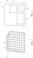
- FIG. 3 is a schematic layout diagram showing a multi-die semiconductor package 1a with a vapor chamber lid 40 according to another embodiment.
- FIG. 4 is a schematic, cross-sectional diagram of the multi-die semiconductor package taken along line I-I' of FIG. 3 , wherein like layers, regions or elements are designated by like numeral numbers or labels.
- the semiconductor package 1a comprises a substrate SB such as a package substrate having a top surface S1 and a bottom surface S2. At least three semiconductor devices 10a, 10b and 10c are mounted on the top surface S1 of the substrate SB in a flip-chip manner. Each of the semiconductor devices 10a-10c has an active front surface S3 directly facing the substrate SB, and an opposite rear surface S4. Preferably, the semiconductor devices 10a-10c may comprise a semiconductor die or a semiconductor package, but is not limited thereto.
- the semiconductor devices 10a-10c may be adjoined to the top surface S1 of the substrate SB using a plurality of connecting elements 12, for example, solder bumps, metal bumps, metal pillars, or micro-bumps.
- the semiconductor package 1a may be mounted onto a printed circuit board (PCB) 2 through a plurality of solder balls or BGA balls 22 distributed on the bottom surface S2 of the substrate SB.
- PCB printed circuit board
- a stiffener ring 30 is mounted on the top surface S1 of the substrate SB.
- the stiffener ring 30 surrounds the semiconductor devices 10a-10c.
- the stiffener ring 30 may be secured to the top surface S1 of the substrate SB by using an adhesive layer (not shown), but is not limited thereto.
- the stiffener ring 30 may be disposed along the perimeter of the substrate SB so as to form a rectangular shape when viewed from the above, for example.
- the stiffener ring 30 may be composed of copper, but is not limited thereto.
- the vapor chamber lid 40 is adhered to the stiffener ring 30 by using, for example, an adhesive layer (not shown), but is not limited thereto.
- the vapor chamber lid 40 is in thermal contact with the rear surface S4 of each of the semiconductor devices 10a-10c.
- a layer of thermal interface material or thermal conductive glue TL may be disposed between the vapor chamber lid 40 and the rear surface S4 of each of the semiconductor devices 10a-10c.
- the vapor chamber lid 40 comprises an internal vacuum-sealed cavity SC that stores a working fluid F, and wick structures WS for recirculating the working fluid F within the internal vacuum-sealed cavity SC.
- the vapor chamber lid 40 may be formed of copper or aluminum, but is not limited thereto.
- the working fluid F may comprise water or deionized water under partial vacuum.
- the wick structures WS may comprise pillar-shaped wicks and may comprises differing distribution density across the vacuum-sealed cavity SC to adapt to a power map of the semiconductor devices10a-10c.
- the wick structures WS may have a lower density in a region directly over the semiconductor devices 10a-10c and a higher density in a region far away from the semiconductor devices 10a-10c.
- the wick structures may be formed by weaving metal wires having a large amount of pores.
- the wick structures may be formed by sintering of copper powder. Copper is often chosen as the wick material since it has a high thermal conductivity enabling to transfer high heat fluxes from the evaporator wall to the working fluid.
- the wick structures WS may comprise porous metallic wicks, such as porous copper wicks.
- the wick structures WS may comprise porous wick structures that generate a capillary pressure to recirculate the working fluid F between an evaporator side ES and a condenser side CS of the vapor chamber lid 40.
- a heat sink 50 may be mounted on the vapor chamber lid 40 and in thermal contact with the condenser side CS of the vapor chamber lid 40.
Landscapes
- Cooling Or The Like Of Semiconductors Or Solid State Devices (AREA)
Abstract
Description
- This application claims the benefit of
U.S. Provisional Application No. 63/324,210, filed on March 28th, 2022 - The present disclosure relates to the field of semiconductor technology. More particularly, the present disclosure relates to a semiconductor package with a vapor chamber lid capable of increasing heat spreading capability and thermal performance.
- For high-performance computing (HPC) applications, high-performance flip-chip ball grid array (HFCBGA) is a common package type, which has the advantage of high reliability and low package stress. As the process node progresses, the die size becomes smaller, which brings in the thermal problem like high power density or local hot spot issues.
- Modern processors and other active components generate high degrees of heat, and traditional cooling methods can no longer keep operating temperatures sufficiently low. Therefore, there is a need in this industry to provide a more effective cooling solution for the semiconductor packages.
- One object of the present invention is to provide a semiconductor package with a vapor chamber lid capable of spreading heat from sources that generate large total heat loads and/or high-power-density hotspots. A semiconductor package according to the invention is defined in
claim 1. The dependent claims define preferred embodiments thereof. - One aspect of the invention provides a semiconductor package including a substrate having a top surface and a bottom surface; a semiconductor device mounted on the top surface of the substrate, the semiconductor device having an active front surface directly facing the substrate, and an opposite rear surface; and a vapor chamber lid in thermal contact with the rear surface of the semiconductor device. The vapor chamber lid comprises an internal vacuum-sealed cavity that stores a working fluid, and wick structures for recirculating the working fluid within the internal vacuum-sealed cavity.
- Preferably, the wick structures are porous wick structures that generate a capillary pressure to recirculate the working fluid between an evaporator side and a condenser side of the vapor chamber lid.
- Preferably, the semiconductor package further includes a stiffener ring mounted on the top surface of the substrate, wherein the stiffener ring surrounds the semiconductor device.
- Preferably, the vapor chamber lid is adhered to the stiffener ring.
- Preferably, the semiconductor package further includes a heat sink mounted on the vapor chamber lid and in thermal contact with the condenser side of the vapor chamber lid.
- Preferably, the vapor chamber lid comprises copper or aluminum.
- Preferably, the working fluid comprises water.
- Preferably, the wick structures comprise porous copper wicks.
- Preferably, the semiconductor device is adjoined to the top surface of the substrate using a plurality of connecting elements.
- Preferably, the semiconductor device comprises a semiconductor die or a semiconductor package, and wherein the substrate comprises a package substrate.
- Another aspect of the invention provides a semiconductor package including a substrate having a top surface and a bottom surface; a plurality of semiconductor devices mounted on the top surface of the substrate, wherein each of the plurality of semiconductor devices has an active front surface directly facing the substrate, and an opposite rear surface; and a vapor chamber lid in thermal contact with a rear surface of each of the plurality of semiconductor devices. The vapor chamber lid comprises an internal vacuum-sealed cavity that stores a working fluid, and wick structures for recirculating the working fluid within the internal vacuum-sealed cavity. The wick structures have a differing distribution density across the internal vacuum-sealed cavity to adapt to a power map of the plurality of semiconductor devices.
- Preferably, the wick structures are porous wick structures that generate a capillary pressure to recirculate the working fluid between an evaporator side and a condenser side of the vapor chamber lid.
- Preferably, the semiconductor package further includes a stiffener ring mounted on the top surface of the substrate, wherein the stiffener ring surrounds the semiconductor device.
- Preferably, the vapor chamber lid is adhered to the stiffener ring.
- Preferably, the semiconductor package further includes a heat sink mounted on the vapor chamber lid and in thermal contact with the condenser side of the vapor chamber lid.
- Preferably, the vapor chamber lid comprises copper or aluminum.
- Preferably, the working fluid comprises water.
- Preferably, the wick structures comprise porous copper wicks.
- Preferably, the semiconductor device is adjoined to the top surface of the substrate using a plurality of connecting elements.
- Preferably, the wick structures have a lower density in a region directly over the plurality of semiconductor devices and a higher density in a region far away from the plurality of semiconductor devices.
- These and other objectives of the present invention will no doubt become obvious to those of ordinary skill in the art after reading the following detailed description of the preferred embodiment that is illustrated in the various figures and drawings.
- The accompanying drawings are included to provide a further understanding of the invention and are incorporated in and constitute a part of this specification. The drawings illustrate embodiments of the invention and, together with the description, serve to explain the principles of the invention. In the drawings:
-
FIG. 1 is a cross-sectional, schematic diagram showing a semiconductor package with a vapor chamber lid according to one embodiment; -
FIG. 2 is a perspective view showing the pillar-shaped wick structures within the vapor chamber lid according to one embodiment; -
FIG. 3 is a schematic layout diagram showing a multi-die semiconductor package with a vapor chamber lid according to another embodiment; and -
FIG. 4 is a schematic, cross-sectional diagram of the multi-die semiconductor package taken along line I-I' ofFIG. 3 . - In the following detailed description of embodiments of the invention, reference is made to the accompanying drawings, which form a part hereof, and in which is shown by way of illustration specific preferred embodiments in which the disclosure may be practiced.
- These embodiments are described in sufficient detail to enable those skilled in the art to practice them, and it is to be understood that other embodiments may be utilized and that mechanical, chemical, electrical, and procedural changes may be made without departing from the scope of the present disclosure. The following detailed description is, therefore, not to be taken in a limiting sense, and the scope of embodiments of the present invention is defined only by the appended claims.
- It will be understood that when an element or layer is referred to as being "on", "connected to" or "coupled to" another element or layer, it can be directly on, connected or coupled to the other element or layer or intervening elements or layers may be present. In contrast, when an element is referred to as being "directly on," "directly connected to" or "directly coupled to" another element or layer, there are no intervening elements or layers present. Like numbers refer to like elements throughout. As used herein, the term "and/or" includes any and all combinations of one or more of the associated listed items.
- An IC die is typically mounted in a package that is attached to a printed circuit board (PCB). One such type of IC die package is a flip chip package. Flip chip is a technology in which electrically conductive elements, such as solder bumps, connect the IC die or the IC die package to a substrate or a PCB. The IC die is flipped over, so that the solder bumps are aligned with corresponding connection sites on the substrate. The solder bumps are reflow soldered to the corresponding connection sites. A flip chip IC die has pads on the active surface of the die, rather than the peripheral bond pads generally associated with a wirebond IC die. The pads on the active face of the flip chip IC die can connect to input/output (I/O), power, or ground.
- A heat spreader may be attached to the non-active surface of the flip chip IC die to facilitate dissipation of heat from the flip chip IC die. The heat spreader can be adhered to the non-active surface of the flip chip IC die using a thermally conductive adhesive, for example. Such heat spreaders rely on dissipation of heat into the ambient air. Current thermal management strategies may rely on spreading high local heat fluxes by conduction in the package lid, ultimately dissipating the total heat load using a mounted heat sink. However, the thermal resistance of the thermal path from the flip chip IC die to the heat sink is often high enough that it becomes the limiting factor for power dissipation. The present invention addresses this issue.
-
FIG. 1 is a cross-sectional, schematic diagram showing asemiconductor package 1 with avapor chamber lid 40 according to one embodiment. As shown inFIG. 1 , thesemiconductor package 1 comprises a substrate SB such as a package substrate having a top surface S1 and a bottom surface S2. At least asemiconductor device 10 is mounted on the top surface S1 of the substrate SB in a flip-chip manner. Thesemiconductor device 10 has an active front surface S3 directly facing the substrate SB, and an opposite rear surface S4. Preferably, thesemiconductor device 10 may comprise a semiconductor die or a semiconductor package, but is not limited thereto. The semiconductor package may comprise one die or multiple die, which may be packaged by using different package types including, but not limited to, flip-chip, wire bonding, or fan-out package. - Preferably, the
semiconductor device 10 may be adjoined to the top surface S1 of the substrate SB using a plurality of connectingelements 12, for example, solder bumps, metal bumps, metal pillars, or micro-bumps. Preferably, thesemiconductor package 1 may be mounted onto a printed circuit board (PCB) 2 through a plurality of solder balls orBGA balls 22 distributed on the bottom surface S2 of the substrate SB. - Preferably, a
stiffener ring 30 is mounted on thetop surface S 1 of the substrate SB. Thestiffener ring 30 surrounds thesemiconductor device 10. Preferably, thestiffener ring 30 may be secured to the top surface S1 of the substrate SB by using an adhesive layer (not shown), but is not limited thereto. Thestiffener ring 30 may be disposed along the perimeter of the substrate SB so as to form a rectangular shape when viewed from the above, for example. Thestiffener ring 30 may be composed of copper, but is not limited thereto. - Preferably, the
vapor chamber lid 40 is adhered to thestiffener ring 30 by using, for example, an adhesive layer (not shown), but is not limited thereto. Preferably, thevapor chamber lid 40 is in thermal contact with the rear surface S4 of thesemiconductor device 10. Preferably, for example, a layer of thermal interface material or thermal conductive glue TL may be disposed between thevapor chamber lid 40 and the rear surface S4 of thesemiconductor device 10. - Preferably, the
vapor chamber lid 40 comprises an internal vacuum-sealed cavity SC that stores a working fluid F, and wick structures WS for recirculating the working fluid F within the internal vacuum-sealed cavity SC. Preferably, for example, thevapor chamber lid 40 may be formed of copper or aluminum, but is not limited thereto. Preferably, for example, the working fluid F may comprise water or deionized water under partial vacuum. - Preferably, as shown in
FIG. 2 , the wick structures WS may comprise pillar-shaped wicks and may comprises differing distribution density across the vacuum-sealed cavity SC. For example, the wick structures WS may have a lower density in a region directly over thesemiconductor device 10 and a higher density in a region far away from thesemiconductor device 10. - Preferably, for example, the wick structures WS may comprise porous copper wicks. Preferably, the wick structures WS may comprise porous wick structures that generate a capillary pressure to recirculate the working fluid F between an evaporator side ES and a condenser side CS of the
vapor chamber lid 40. Preferably, optionally, aheat sink 50 may be mounted on thevapor chamber lid 40 and in thermal contact with the condenser side CS of thevapor chamber lid 40. - The thermal resistance to lateral flow of heat flux through the
lid 40 of thesemiconductor package 1 may be reduced by incorporating vapor chamber into the lid itself. This has the further benefit of reducing the effective thermal resistance of the mechanical interface between the lid of the package and theexternal heat sink 50. The vapor chamber makes the lid a better thermal path from thesemiconductor device 10 to theheat sink 50. - Please refer to
FIG. 3 andFIG. 4 .FIG. 3 is a schematic layout diagram showing a multi-die semiconductor package 1a with avapor chamber lid 40 according to another embodiment.FIG. 4 is a schematic, cross-sectional diagram of the multi-die semiconductor package taken along line I-I' ofFIG. 3 , wherein like layers, regions or elements are designated by like numeral numbers or labels. - As shown in
FIG. 3 andFIG. 4 , likewise, the semiconductor package 1a comprises a substrate SB such as a package substrate having a top surface S1 and a bottom surface S2. At least threesemiconductor devices semiconductor devices 10a-10c has an active front surface S3 directly facing the substrate SB, and an opposite rear surface S4. Preferably, thesemiconductor devices 10a-10c may comprise a semiconductor die or a semiconductor package, but is not limited thereto. - Preferably, the
semiconductor devices 10a-10c may be adjoined to the top surface S1 of the substrate SB using a plurality of connectingelements 12, for example, solder bumps, metal bumps, metal pillars, or micro-bumps. Preferably, the semiconductor package 1a may be mounted onto a printed circuit board (PCB) 2 through a plurality of solder balls orBGA balls 22 distributed on the bottom surface S2 of the substrate SB. - Preferably, a
stiffener ring 30 is mounted on the top surface S1 of the substrate SB. Thestiffener ring 30 surrounds thesemiconductor devices 10a-10c. Preferably, thestiffener ring 30 may be secured to the top surface S1 of the substrate SB by using an adhesive layer (not shown), but is not limited thereto. Thestiffener ring 30 may be disposed along the perimeter of the substrate SB so as to form a rectangular shape when viewed from the above, for example. Thestiffener ring 30 may be composed of copper, but is not limited thereto. - Preferably, the
vapor chamber lid 40 is adhered to thestiffener ring 30 by using, for example, an adhesive layer (not shown), but is not limited thereto. Preferably, thevapor chamber lid 40 is in thermal contact with the rear surface S4 of each of thesemiconductor devices 10a-10c. Preferably, for example, a layer of thermal interface material or thermal conductive glue TL may be disposed between thevapor chamber lid 40 and the rear surface S4 of each of thesemiconductor devices 10a-10c. - Preferably, the
vapor chamber lid 40 comprises an internal vacuum-sealed cavity SC that stores a working fluid F, and wick structures WS for recirculating the working fluid F within the internal vacuum-sealed cavity SC. Preferably, for example, thevapor chamber lid 40 may be formed of copper or aluminum, but is not limited thereto. Preferably, for example, the working fluid F may comprise water or deionized water under partial vacuum. - Preferably, the wick structures WS may comprise pillar-shaped wicks and may comprises differing distribution density across the vacuum-sealed cavity SC to adapt to a power map of the semiconductor devices10a-10c. For example, the wick structures WS may have a lower density in a region directly over the
semiconductor devices 10a-10c and a higher density in a region far away from thesemiconductor devices 10a-10c. - Preferably, the wick structures may be formed by weaving metal wires having a large amount of pores. Preferably, the wick structures may be formed by sintering of copper powder. Copper is often chosen as the wick material since it has a high thermal conductivity enabling to transfer high heat fluxes from the evaporator wall to the working fluid.
- Preferably, for example, the wick structures WS may comprise porous metallic wicks, such as porous copper wicks. Preferably, the wick structures WS may comprise porous wick structures that generate a capillary pressure to recirculate the working fluid F between an evaporator side ES and a condenser side CS of the
vapor chamber lid 40. Preferably, optionally, aheat sink 50 may be mounted on thevapor chamber lid 40 and in thermal contact with the condenser side CS of thevapor chamber lid 40. - Those skilled in the art will readily observe that numerous modifications and alterations of the device and method may be made while retaining the teachings of the invention. Accordingly, the above disclosure should be construed as limited only by the metes and bounds of the appended claims.
Claims (12)
- A semiconductor package (1; 1a), comprising:a substrate (SB) having a top surface (S1) and a bottom surface (S2);a semiconductor device (10; 10a - 10c) mounted on the top surface (S1) of the substrate (SB), the semiconductor device (10; 10a - 10c) having an active front surface (S3) directly facing the substrate (SB), and an opposite rear surface (S4); anda vapor chamber lid (40) in thermal contact with the rear surface (S4) of the semiconductor device (10; 10a - 10c), wherein the vapor chamber lid (40) comprises an internal vacuum-sealed cavity (SC) that stores a working fluid (F), and wick structures (WS) for recirculating the working fluid (F) within the internal vacuum-sealed cavity (SC).
- The semiconductor package (1; 1a) according to claim 1, wherein the wick structures (WS) are porous wick structures that generate a capillary pressure to recirculate the working fluid (F) between an evaporator side (ES) and a condenser side (CS) of the vapor chamber lid (40).
- The semiconductor package (1; 1a) according to claim 1 or 2, further comprising:
a stiffener ring (30) mounted on the top surface (S1) of the substrate (SB), wherein the stiffener ring (30) surrounds the semiconductor device (10; 10a - 10c). - The semiconductor package (1; 1a) according to claim 3, wherein the vapor chamber lid (40) is adhered to the stiffener ring (30).
- The semiconductor package (1; 1a) according to claim 2 or according to claim 3 or 4 in combination with claim 2, further comprising:
a heat sink (50) mounted on the vapor chamber lid (40) and in thermal contact with the condenser side (CS) of the vapor chamber lid (40). - The semiconductor package (1; 1a) according to any one of claims 1 to 5, wherein the vapor chamber lid (40) comprises copper or aluminum.
- The semiconductor package (1; 1a) according to any one of claims 1 to 6, wherein the working fluid (F) comprises water.
- The semiconductor package (1; 1a) according to any one of claims 1 to 7, wherein the wick structures (WS) comprise porous copper wicks.
- The semiconductor package (1; 1a) according to any one of claims 1 to 8, wherein the semiconductor device (10; 10a - 10c) is adjoined to the top surface (S1) of the substrate (SB) using a plurality of connecting elements (12).
- The semiconductor package (1; 1a) according to any one of claims 1 to 9, wherein the semiconductor device (10; 10a - 10c) comprises a semiconductor die or a semiconductor package, and wherein the substrate (SB) comprises a package substrate.
- The semiconductor package (1a) according to any one of claims 1 to 10, comprising:a plurality of semiconductor devices (10a - 10c) mounted on the top surface (S1) of the substrate (SB), wherein each of the plurality of semiconductor devices (10a - 10c) has an active front surface (S3) directly facing the substrate (SB), and an opposite rear surface (S4); whereinthe vapor chamber lid (40) is in thermal contact with the rear surface (S4) of each of the plurality of semiconductor devices (10a - 10c), wherein the wick structures (WS) have a differing distribution density across the internal vacuum-sealed cavity (SC) to adapt to a power map of the plurality of semiconductor devices (10a - 10c).
- The semiconductor package (1; 1a) according to claim 11, wherein the wick structures (WS) have a lower density in a region directly over the plurality of semiconductor devices (10a - 10c) and a higher density in a region far away from the plurality of semiconductor devices (10a - 10c).
Applications Claiming Priority (2)
| Application Number | Priority Date | Filing Date | Title |
|---|---|---|---|
| US202263324210P | 2022-03-28 | 2022-03-28 | |
| US18/116,258 US20230307316A1 (en) | 2022-03-28 | 2023-03-01 | Semiconductor package with vapor chamber lid |
Publications (1)
| Publication Number | Publication Date |
|---|---|
| EP4253891A1 true EP4253891A1 (en) | 2023-10-04 |
Family
ID=85601587
Family Applications (1)
| Application Number | Title | Priority Date | Filing Date |
|---|---|---|---|
| EP23161493.4A Pending EP4253891A1 (en) | 2022-03-28 | 2023-03-13 | Semiconductor package with vapor chamber lid |
Country Status (3)
| Country | Link |
|---|---|
| US (1) | US20230307316A1 (en) |
| EP (1) | EP4253891A1 (en) |
| TW (1) | TW202339151A (en) |
Families Citing this family (1)
| Publication number | Priority date | Publication date | Assignee | Title |
|---|---|---|---|---|
| TWI866712B (en) * | 2023-12-21 | 2024-12-11 | 矽品精密工業股份有限公司 | Heat dissipation structure and electronic package thereof |
Citations (13)
| Publication number | Priority date | Publication date | Assignee | Title |
|---|---|---|---|---|
| US20050280162A1 (en) * | 2004-06-18 | 2005-12-22 | International Business Machines Corporation | Thermal interposer for thermal management of semiconductor devices |
| US20060219391A1 (en) * | 2005-04-01 | 2006-10-05 | Chu-Wan Hong | Heat pipe with sintered powder wick |
| US20090056917A1 (en) * | 2005-08-09 | 2009-03-05 | The Regents Of The University Of California | Nanostructured micro heat pipes |
| JP2015010765A (en) * | 2013-06-28 | 2015-01-19 | トヨタ自動車株式会社 | Vapor chamber and method for manufacturing vapor chamber |
| US20190014688A1 (en) * | 2015-12-11 | 2019-01-10 | Purdue Research Foundation | Vapor chamber heat spreaders and methods of manufacturng thereof |
| US20190039883A1 (en) * | 2017-08-01 | 2019-02-07 | Analog Devices Global | Monolithic phase change heat sink |
| US20190348345A1 (en) * | 2018-05-10 | 2019-11-14 | International Business Machines Corporation | Module Lid with Embedded Two-Phase Cooling and Insulating Layer |
| CN110828404A (en) * | 2019-11-22 | 2020-02-21 | 华南理工大学 | A microchannel vapor chamber with a cavity structure |
| CN111473671A (en) * | 2020-04-21 | 2020-07-31 | 福建永安市永清石墨烯研究院有限公司 | Graphene VC soaking plate and preparation method thereof |
| CN111780603A (en) * | 2020-08-21 | 2020-10-16 | 北京中石伟业科技无锡有限公司 | A large flat soaking plate of composite liquid absorbing core |
| CN212458063U (en) * | 2020-05-29 | 2021-02-02 | 武汉大学 | A self-wetting fluid-coupled composite absorbent core soaking plate |
| US20210041182A1 (en) * | 2019-08-06 | 2021-02-11 | Intel Corporation | Thermal management in integrated circuit packages |
| US20210372709A1 (en) * | 2020-05-26 | 2021-12-02 | Purdue Research Foundation | Vapor chamber devices and methods of dissipating heat therewith |
Family Cites Families (1)
| Publication number | Priority date | Publication date | Assignee | Title |
|---|---|---|---|---|
| US10978373B2 (en) * | 2018-06-19 | 2021-04-13 | Taiwan Semiconductor Manufacturing Company, Ltd. | Semiconductor device methods of manufacture |
-
2023
- 2023-03-01 US US18/116,258 patent/US20230307316A1/en active Pending
- 2023-03-13 EP EP23161493.4A patent/EP4253891A1/en active Pending
- 2023-03-28 TW TW112111733A patent/TW202339151A/en unknown
Patent Citations (13)
| Publication number | Priority date | Publication date | Assignee | Title |
|---|---|---|---|---|
| US20050280162A1 (en) * | 2004-06-18 | 2005-12-22 | International Business Machines Corporation | Thermal interposer for thermal management of semiconductor devices |
| US20060219391A1 (en) * | 2005-04-01 | 2006-10-05 | Chu-Wan Hong | Heat pipe with sintered powder wick |
| US20090056917A1 (en) * | 2005-08-09 | 2009-03-05 | The Regents Of The University Of California | Nanostructured micro heat pipes |
| JP2015010765A (en) * | 2013-06-28 | 2015-01-19 | トヨタ自動車株式会社 | Vapor chamber and method for manufacturing vapor chamber |
| US20190014688A1 (en) * | 2015-12-11 | 2019-01-10 | Purdue Research Foundation | Vapor chamber heat spreaders and methods of manufacturng thereof |
| US20190039883A1 (en) * | 2017-08-01 | 2019-02-07 | Analog Devices Global | Monolithic phase change heat sink |
| US20190348345A1 (en) * | 2018-05-10 | 2019-11-14 | International Business Machines Corporation | Module Lid with Embedded Two-Phase Cooling and Insulating Layer |
| US20210041182A1 (en) * | 2019-08-06 | 2021-02-11 | Intel Corporation | Thermal management in integrated circuit packages |
| CN110828404A (en) * | 2019-11-22 | 2020-02-21 | 华南理工大学 | A microchannel vapor chamber with a cavity structure |
| CN111473671A (en) * | 2020-04-21 | 2020-07-31 | 福建永安市永清石墨烯研究院有限公司 | Graphene VC soaking plate and preparation method thereof |
| US20210372709A1 (en) * | 2020-05-26 | 2021-12-02 | Purdue Research Foundation | Vapor chamber devices and methods of dissipating heat therewith |
| CN212458063U (en) * | 2020-05-29 | 2021-02-02 | 武汉大学 | A self-wetting fluid-coupled composite absorbent core soaking plate |
| CN111780603A (en) * | 2020-08-21 | 2020-10-16 | 北京中石伟业科技无锡有限公司 | A large flat soaking plate of composite liquid absorbing core |
Also Published As
| Publication number | Publication date |
|---|---|
| TW202339151A (en) | 2023-10-01 |
| US20230307316A1 (en) | 2023-09-28 |
Similar Documents
| Publication | Publication Date | Title |
|---|---|---|
| US11967570B2 (en) | Semiconductor package having improved thermal interface between semiconductor die and heat spreading structure | |
| US11594469B2 (en) | Semiconductor device and method of manufacture | |
| US8970029B2 (en) | Thermally enhanced heat spreader for flip chip packaging | |
| US5880524A (en) | Heat pipe lid for electronic packages | |
| US6681482B1 (en) | Heatspreader for a flip chip device, and method for connecting the heatspreader | |
| US6535388B1 (en) | Wirebonded microelectronic packages including heat dissipation devices for heat removal from active surfaces thereof | |
| US8373991B2 (en) | Metal thermal interface material and thermal module and packaged microelectronic component containing the material | |
| US7611923B2 (en) | Method and apparatus for forming stacked die and substrate structures for increased packing density | |
| US8022534B2 (en) | Semiconductor package using an active type heat-spreading element | |
| US20060060952A1 (en) | Heat spreader for non-uniform power dissipation | |
| US12278150B2 (en) | Semiconductor package with annular package lid structure | |
| TW578282B (en) | Thermal- enhance MCM package | |
| CN119447039A (en) | Electronic packaging and method of manufacturing the same | |
| US11973000B2 (en) | Heat dissipation plate and semiconductor device | |
| US20230307316A1 (en) | Semiconductor package with vapor chamber lid | |
| CN116825730A (en) | Semiconductor packaging | |
| US20080164604A1 (en) | Heat dissipating semiconductor package | |
| EP4456128A1 (en) | Thermal management systems and methods for semiconductor devices | |
| JP2008016653A (en) | Semiconductor package, manufacturing method thereof, printed circuit board, and electronic device | |
| CN101276795B (en) | Semiconductor Package Structure | |
| CN222088581U (en) | Electronic package | |
| US20040032025A1 (en) | Flip chip package with thermometer | |
| US20240421026A1 (en) | Electronic package and manufacturing method thereof | |
| KR20050031599A (en) | Semiconductor package having thermal interface material | |
| CN211238226U (en) | Power Semiconductor Packaged Devices |
Legal Events
| Date | Code | Title | Description |
|---|---|---|---|
| PUAI | Public reference made under article 153(3) epc to a published international application that has entered the european phase |
Free format text: ORIGINAL CODE: 0009012 |
|
| STAA | Information on the status of an ep patent application or granted ep patent |
Free format text: STATUS: THE APPLICATION HAS BEEN PUBLISHED |
|
| AK | Designated contracting states |
Kind code of ref document: A1 Designated state(s): AL AT BE BG CH CY CZ DE DK EE ES FI FR GB GR HR HU IE IS IT LI LT LU LV MC ME MK MT NL NO PL PT RO RS SE SI SK SM TR |
|
| STAA | Information on the status of an ep patent application or granted ep patent |
Free format text: STATUS: REQUEST FOR EXAMINATION WAS MADE |
|
| 17P | Request for examination filed |
Effective date: 20240403 |
|
| RBV | Designated contracting states (corrected) |
Designated state(s): AL AT BE BG CH CY CZ DE DK EE ES FI FR GB GR HR HU IE IS IT LI LT LU LV MC ME MK MT NL NO PL PT RO RS SE SI SK SM TR |