EP4241051B1 - Persistence filtering in spd arrays - Google Patents
Persistence filtering in spd arrays Download PDFInfo
- Publication number
- EP4241051B1 EP4241051B1 EP22777201.9A EP22777201A EP4241051B1 EP 4241051 B1 EP4241051 B1 EP 4241051B1 EP 22777201 A EP22777201 A EP 22777201A EP 4241051 B1 EP4241051 B1 EP 4241051B1
- Authority
- EP
- European Patent Office
- Prior art keywords
- spd
- observation
- previous
- windows
- calibration
- Prior art date
- Legal status (The legal status is an assumption and is not a legal conclusion. Google has not performed a legal analysis and makes no representation as to the accuracy of the status listed.)
- Active
Links
Images




Classifications
-
- G—PHYSICS
- G01—MEASURING; TESTING
- G01J—MEASUREMENT OF INTENSITY, VELOCITY, SPECTRAL CONTENT, POLARISATION, PHASE OR PULSE CHARACTERISTICS OF INFRARED, VISIBLE OR ULTRAVIOLET LIGHT; COLORIMETRY; RADIATION PYROMETRY
- G01J1/00—Photometry, e.g. photographic exposure meter
- G01J1/42—Photometry, e.g. photographic exposure meter using electric radiation detectors
- G01J1/44—Electric circuits
-
- H—ELECTRICITY
- H04—ELECTRIC COMMUNICATION TECHNIQUE
- H04N—PICTORIAL COMMUNICATION, e.g. TELEVISION
- H04N23/00—Cameras or camera modules comprising electronic image sensors; Control thereof
- H04N23/95—Computational photography systems, e.g. light-field imaging systems
-
- H—ELECTRICITY
- H04—ELECTRIC COMMUNICATION TECHNIQUE
- H04N—PICTORIAL COMMUNICATION, e.g. TELEVISION
- H04N25/00—Circuitry of solid-state image sensors [SSIS]; Control thereof
- H04N25/60—Noise processing, e.g. detecting, correcting, reducing or removing noise
-
- H—ELECTRICITY
- H04—ELECTRIC COMMUNICATION TECHNIQUE
- H04N—PICTORIAL COMMUNICATION, e.g. TELEVISION
- H04N25/00—Circuitry of solid-state image sensors [SSIS]; Control thereof
- H04N25/70—SSIS architectures; Circuits associated therewith
- H04N25/76—Addressed sensors, e.g. MOS or CMOS sensors
- H04N25/77—Pixel circuitry, e.g. memories, A/D converters, pixel amplifiers, shared circuits or shared components
- H04N25/772—Pixel circuitry, e.g. memories, A/D converters, pixel amplifiers, shared circuits or shared components comprising A/D, V/T, V/F, I/T or I/F converters
- H04N25/773—Pixel circuitry, e.g. memories, A/D converters, pixel amplifiers, shared circuits or shared components comprising A/D, V/T, V/F, I/T or I/F converters comprising photon counting circuits, e.g. single photon detection [SPD] or single photon avalanche diodes [SPAD]
-
- H—ELECTRICITY
- H10—SEMICONDUCTOR DEVICES; ELECTRIC SOLID-STATE DEVICES NOT OTHERWISE PROVIDED FOR
- H10F—INORGANIC SEMICONDUCTOR DEVICES SENSITIVE TO INFRARED RADIATION, LIGHT, ELECTROMAGNETIC RADIATION OF SHORTER WAVELENGTH OR CORPUSCULAR RADIATION
- H10F77/00—Constructional details of devices covered by this subclass
- H10F77/95—Circuit arrangements
- H10F77/953—Circuit arrangements for devices having potential barriers
- H10F77/959—Circuit arrangements for devices having potential barriers for devices working in avalanche mode
-
- G—PHYSICS
- G01—MEASURING; TESTING
- G01J—MEASUREMENT OF INTENSITY, VELOCITY, SPECTRAL CONTENT, POLARISATION, PHASE OR PULSE CHARACTERISTICS OF INFRARED, VISIBLE OR ULTRAVIOLET LIGHT; COLORIMETRY; RADIATION PYROMETRY
- G01J1/00—Photometry, e.g. photographic exposure meter
- G01J1/42—Photometry, e.g. photographic exposure meter using electric radiation detectors
- G01J1/44—Electric circuits
- G01J2001/4413—Type
- G01J2001/442—Single-photon detection or photon counting
-
- H—ELECTRICITY
- H04—ELECTRIC COMMUNICATION TECHNIQUE
- H04N—PICTORIAL COMMUNICATION, e.g. TELEVISION
- H04N17/00—Diagnosis, testing or measuring for television systems or their details
- H04N17/002—Diagnosis, testing or measuring for television systems or their details for television cameras
Definitions
- the invention relates to an improved method, detector element and system for high-speed imaging based on single-photon detectors (SPD), whereby false positives are filtered out of the results.
- SPD single-photon detectors
- a light beam typically a laser
- the location where the beam impinges is recorded at each point in time via multiple image sensors.
- the effective distance to the illuminated target can be determined, via triangulation.
- Such a measurement captures a voxel.
- the speed at which this process can be carried out, the voxel rate is limited on the one hand by the speed at which scanning with the light beam takes place, but on the other hand is also (the most strongly) limited by the processing time required by the sensors to detect the reflected light beams, especially in relation to background radiation (ambient light) and general thermal noise.
- a first one is the accuracy with which incident photons are detected.
- Increasingly higher demands are made in terms of spatial resolution, resulting in the sensor arrays having increasingly more separate detectors (pixels).
- This means increased computing power is needed to read all said detectors and to process the output signals into an image.
- the separate pixels always (have to) become smaller, the photosensitivity must also increase, as they have a limited spatial window to capture photons.
- the senor must also be suitable for operating with limited photon budgets (i.e. detected photons incident on the sensor that are sufficient for a detection), such as, for example, 10 photons. Given the limited time span for processing, only a limited number of photons can be captured.
- limited photon budgets i.e. detected photons incident on the sensor that are sufficient for a detection
- SPDs single photon - avalanche - detectors
- said detectors have the inherent disadvantage that the increased photosensitivity also causes unwanted excitations, both due to ambient light and due to thermal noise. In itself such excitations on detector level are difficult to distinguish from 'genuine' detections resulting from the incidence of reflected light that was deliberately emitted by the system to scan a scene.
- a time-of-flight (TOF) sensor includes a light source, a plurality of avalanche photodiodes, and a plurality of pulse generators.
- Control circuitry is coupled to the light source, the plurality of avalanche photodiodes, and the plurality of pulse generators, and the control circuitry includes logic that when executed by the control circuitry causes the time-of-flight sensor to perform operations.
- the operations include emitting the light from the light source, and receiving the light reflected from an object with the plurality of avalanche photodiodes.
- a plurality of pulses is output from the individual pulse generators corresponding to the individual avalanche photodiodes that received the light, and a timing signal is output when the plurality of pulses overlap temporally.
- a time is calculated when a first avalanche photodiode in the plurality of avalanche photodiodes received the light.
- a vision sensor includes a pixel array comprising pixels arranged in a matrix, an event detection circuit, an event rate controller, and an interface circuit. Each pixel is configured to generate an electrical signal in response to detecting a change in incident light intensity.
- the event detection circuit detects whether a change in incident light intensity has occurred at any pixels, based on processing electrical signals received from one or more pixels, and generates one or more event signals corresponding to one or more pixels at which a change in intensity of incident light is determined to have occurred.
- the event rate controller selects a selection of one or more event signals corresponding to a region of interest on the pixel array as one or more output event signals.
- the interface circuit communicates with an external processor to transmit the one or more output event signals to the external processor.
- the purpose of the present invention is to find a solution for at least a number of the aforementioned problems.
- the invention relates to an improved high-speed imaging method according to claim 1.
- each photon impinging on an SPD or SPAD generates a detection signal, as said components are specifically designed to be able to also record their incidence in case of low photon densities, which benefits the speed and resolution.
- the smaller SPD/SPAD surface allows more SPD/SPAD per surface and therefore a higher resolution, but therefore also lowers the risk of photon incidence, such that the sensitivity of the components must lie higher, and thus trigger them faster.
- the purpose of the present invention is to recognise said false positives and filter them out of the results, and only confirm the 'real' photon incidences (coming from an active illumination of an object or scene by a light source of the system).
- the invention in a second aspect relates to a detector element and a sensor system for high-speed imaging, preferably suitable for executing the method according to the first aspect, as specified in claims 12, and 13 and 14.
- a segment means one or more than a segment.
- pixel refers to a light-sensitive unit or detector here, preferably in the form of an SPD or SPAD. Typically, said pixels are provided in an array like a matrix.
- macropixel hereby refers to a virtual pixel comprising several pixels or detectors, which typically form a contiguous cluster. Said macropixel may be associated to a certain set of spatiotemporal conditions, and vary depending on the circumstances in terms of size, form and other parameters. Macropixels can partially overlap with each other, and have pixels or detectors in common. Preferably, a macropixel has a square or rectangular form, but can also be approximately circular or oval, triangular, cross- or star-shaped, or have other forms.
- a macropixel comprises at least 2 detectors (e.g. in 2 ⁇ 1 or 1 ⁇ 2 matrix form), and more preferably at least 4 detectors (e.g. 2 ⁇ 2).
- Quoting numerical intervals by the end points comprises all integers, fractions, and/or real numbers between the end points, including said end points.
- the invention relates to a high-speed imaging method based on an array comprising a plurality of single photon detectors (SPD), preferably single photon avalanche detectors (SPAD), comprising the following steps:
- the persistence condition for at least one, and preferably every, SPD requires a positive observation status for the same SPD in at least M, preferably consecutive, observation windows, preferably with period T, over the past N observation windows, with M greater than 1 and at most equal to N.
- the persistence condition of M (consecutive or not) of the N observation windows can also be applied in alternative ways, among others with a percentage M/N of the past N observation windows (again, with the condition or not that said M are consecutive, whereby M is then typically equal to N).
- the aforementioned method allows 'active' radiation to be consistently detected, because typically said radiation impinges extensively in a certain zone over a certain time period, and thus meets the persistence condition, unlike thermal noise and other unwanted detections.
- the method comprises illuminating a scene with a scanning light source (of which an image must be formed: object, environment, etc.) using one or several light sources (laser, LED, etc.) based on a predefined illumination pattern.
- Said illumination pattern comprises temporally separated light pulses (with constant length and/or interval or not).
- the observation windows based on which the persistence condition is imposed are temporally associated to one of the light pulses, and the detection signal shows the occurrence or non-occurrence of an observation by the SPD (positive observation status or not).
- Temporally associating the observation windows to the light pulses is timing the observation window such (in terms of start and/or end time) that they largely overlap, such that the observed radiation in the observation windows can be linked with very high probability to the light pulses (and thus not to thermal noise or other noise signals).
- N is typically set between 2 and 10, preferably between 2 and 7, more preferably between 2 and 5, such as 2, 3, 4 or 5.
- the observation windows are set to largely overlap with the light pulses to which they are associated (i.e. largely covering the time period of the light pulses, but not necessarily limited hereto), with start times substantially coinciding (and whereby the start time of the observation windows is at the earliest simultaneous with those of the light pulses).
- Substantially coinciding implies that the start time of the observation window lies between 0.0 ns and 1.0 ns after the start time of the light pulse, preferably at most 0.5 ns, and even more preferably at most 0.1 ns or even 0.05 ns. Consequently it is ensured that (practically) all radiation that impinges during the observation window comes from events from the time period of the light pulse.
- the start time allows some play which takes into account time-of-flight.
- the detectors are provided with a quenching circuit. More preferably this is a passive quenching circuit. Alternatively this is an active quenching circuit.
- the observation windows are set with an end time between 0.0 ns and 25.0 ns after the end time of the associated light pulse, preferably between 0.05 ns and 15.0 ns, more preferably between 0.1 ns and 10.0 ns after the end time of the associated light pulse.
- such timing ensures that the radiation coming from events during the time period of the light pulse, is captured in the observation window, taking into account the time-of-flight.
- the method comprises a step of illuminating a scene with one or more scanning light sources, whereby the light sources illuminate the scene substantially continuously.
- the light source illuminates continuously and with a substantially constant intensity.
- the observation windows can be chosen more arbitrarily, and if relevant even contiguously.
- the light sources are used to emit an active and controlled light signal, and consequently to illuminate a scene/object of which an image will be formed.
- the SPDs capture reflected photons and register said incidence based on a detection signal to a further component, to thus form an image of the illuminated scene/object.
- the method thus comprises illuminating a scene or object with the light source(s), whereby the light source illuminates in discrete or quasi-discrete steps, and for each discrete or quasi-discrete position that is illuminated, briefly continues illuminating before going to a next discrete position.
- discrete position herein refers to a discrete orientation of the light source, which comes down to a certain discrete position that is illuminated.
- the 'route' of discrete positions that is followed during illuminating can be randomised, but typically follows a scanning pattern, row per row or column per column. However, it needs to be noted that the invention is not limited in this aspect in any way whatsoever.
- Quadratrete hereby refers to situations in which the light source continues to vary its orientation, but at a speed such that the covered distance of illuminated zones in case of (2 or more) consecutive observation windows is very limited, and can be considered as the same discrete zone. In what follows “discrete” therefore needs to be interpreted as comprising quasi-discrete.
- M and/or N are adjustable, and even more preferably even adjustable per SPD.
- they can be set dynamically, such that the system automatically adapts them on detection of many or few noise detections (detection signals whereby the persistence condition is not met) for an SPD.
- the persistence condition can be relaxed for SPDs where little noise is observed statistically, and tightened where more noise is observed statistically, to thus be able to operate more quickly and accurately.
- Making M and/or N separately adjustable can therefore be used to make certain SPDs more sensitive or less sensitive, such as for example upon detection of many detection windows with detection signals without active light, which may point to a 'leaky pixel'. They can even be completely switched off if necessary.
- M and/or N are automatically adapted based on a calibration routine.
- the persistence condition is combined with meeting a coincidence condition. This builds on the assumption that in the event of observations by the SPD, the incidence of a photon on a certain SPD is not single, but involves the incidence of a bundle of photons that are spatially clustered. Based on this the coincidence condition is imposed which in a certain time period around a positive observation status or a confirmation signal of an SPD verifies the observation status or confirmation signals of neighbouring SPDs.
- the coincidence condition can be imposed before or following the persistence condition, and depending on the circuit is more efficient in one way or another.
- the coincidence condition can be imposed subsequently, and only after it is met a confirmation signal is generated.
- the coincidence condition implies that at least one adjacent SPD (adjacent to the first SPD) also meets the persistence condition. Obviously this can be narrowed to at least 2, 3, 4, etc. of the adjacent SPDs that have to meet the persistence condition.
- adjacent SPD primarily refers to the directly adjacent SPDs.
- the SPDs are typically provided in a rectangular array of rows and columns, which means that the adjacent SPDs are situated in one and the same row and neighbouring column or one and the same column and neighbouring row.
- the term can be simply expanded to comprise for example diagonally adjacent SPDs (neighbouring row and neighbouring column), or even wider still, such that 'opposite neighbours' are also included herein.
- the coincidence condition can be imposed in a number of ways and with variable conditions.
- the number of adjacent SPDs that meet the persistence condition can be adapted (1, 2, 3, 4, 5, 6, 7, 8, 9 or more), but the definition of "adjacent" can also be adapted.
- adjacent can be interpreted as “directly adjacent”, but “diagonally adjacent” SPDs can also be accepted (directly adjacent to a first directly adjacent SPD in another dimension than the first SPD is directly adjacent), and this can also be defined as lying within a predefined interval of the original SPD (and thus also allow opposite neighbours). Again this can be varied depending on the circumstances, and the system can even adapt this dynamically (for example via a calibration routine).
- a first filtering is applied, after which the coincidence condition only has to be applied on the remaining detections that are confirmed according to the persistence condition. This sequence ensures that the computationally most challenging condition (coincidence condition, as it needs to take into account the signals of a number of adjacent SPDs) has to be applied to a lower number of signals.
- the first method means that adjacent SPDs to a first SPD with position (i,j) are simplly defined as having coordinates(i,j ⁇ 1) or (i ⁇ 1,j). To add diagonally adjacent SPDs, SPDs with coordinates (i ⁇ 1,j ⁇ 1) are also accepted.
- adjacent SPDs can thus also be expanded with SPDs with coordinates (i ⁇ 2,j ⁇ 1), (i ⁇ 1,j ⁇ 2), (i ⁇ 2,j), (i,j ⁇ 2), again possibly supplemented by (i ⁇ 2,j ⁇ 2).
- the coincidence condition based on the definition of adjacent SPDs can also be adapted, whereby every SPD is given a weight based on the 'distance' in the array relative to the first SPD. Only on reaching a certain weight in SPDs for which the persistence condition is met, is the coincidence condition considered to be met for the first SPD.
- the coincidence condition can be imposed for an SPD (as described above, but per observation window based on a positive observation status in said observation window instead of meeting the persistence condition), and only for the SPDs where the coincidence condition is met, is meeting the persistence condition subsequently checked.
- the invention in a second aspect relates to a detector element comprising: a single photon detector (SPD), preferably a single photon avalanche detector (SPAD), configured to generate a signal C_ov which describes a status of the occurrence or non-occurrence of an observation by the SPD of the electromagnetic radiation (photons) to be detected for consecutive observation windows; a memory element that remembers the status of the SPD at the end of at least N previous observation windows, N being a natural number equal to or greater than 1; a logical circuit configured to generate a confirmation signal if the signal of the SPD at the end of a current observation window and of at least M of the N previous observation windows indicates an observation by the SPD , M being a natural number equal to or greater than 1 and at most equal to N.
- SPD single photon detector
- SPAD single photon avalanche detector
- the persistence condition is executed in a centralised way to keep the detector elements simpler.
- the consecutive light pulses are separated at least 0.5 ns, preferably at least 1.0 ns, even more preferably at least 2.5 ns, and most preferably at least 5.0 ns.
- the consecutive light pulses are separated at most 1000 ns, preferably at most 500 ns, even more preferably at most 100 ns, and most preferably at most 50 ns.
- the highest preference combines the aforementioned minimum and maximum values to a corresponding range.
- the length of the light pulses of the predefined illumination pattern and the length of the associated observation windows have a ratio located between 1.0 and 2.0, preferably between 1.0 and 1.5 and most preferably between 1.0 and 1.25. In this way it is guaranteed that as many as possible signals caused by the light pulses are captured in the observation window, without making this needlessly long (such that the method would be slower).
- observation statuses of the past N windows are saved by memory elements on the SPAD or on a central processing unit (which imposes the persistence condition for several, or even all SPADs of the array), whereby 'obsolete' observation statuses (more than N windows ago) are overwritten by newer ones.
- memory elements may include flipflops, DRAM (dynamic RAM), SRAM (static RAM), analogue memory elements or other components.
- a buffer element Prior to the logical circuit (and memory elements), preferably a buffer element is provided to isolate the operation of SPAD and the processing of the signals from each other.
- a so-called delay circuit can be provided which includes the signal from a previous observation window and feeds it to a logical circuit, such as a simple AND-port, together with the signal of a current observation window.
- a logical circuit such as a simple AND-port
- the persistence condition can be applied locally on the SPAD itself, such that only the (non-) confirmation signal to a further processing unit is provided.
- the invention in a third aspect relates to a sensor system for high-speed imaging, comprising a matrix/array of detector elements according to the second aspect of the invention; and a circuit for reading the detector elements in the matrix/array.
- a sensor system for high-speed imaging in its third aspect comprising:
- the one or more memory elements are hereby configured to remember the status of the SPD at the end of at least N previous observation windows per SPD, N being a natural number equal to or greater than 1.
- the logical circuit is configured to generate a confirmation signal for an SPD if the signal of the SPD at the end of a current observation window and of at least M of the N previous observation windows of the SPD indicate an observation by the SPD , with M being a natural number equal to or greater than 1 and at most equal to N. In this way the detector elements are kept simple (and thus more compact, cheaper, more robust) and the computational load is borne centrally.
- the sensor system is configured for executing a method according to the first aspect of the invention.
- the invention relates to a method for calibrating imaging systems comprising an array which comprises a plurality of single photon detectors (SPD), preferably single photon avalanche detectors (SPAD).
- the method relates to the monitoring of the observation status/detection signals over a calibration time period by an evaluation circuit (either with one evaluation circuit or per SPD, per group of SPDs or for the whole system), in at least two, preferably at least three calibration windows in the calibration time period.
- the calibration windows are temporally separated from each other, and run during periods in which the array of SPDs is not actively illuminated (i.e. deliberately with light sources controlled by the system).
- the number of calibration windows can be set higher, and thus allow a more thorough and reliable classification, for example, 5, 6, 7, 8, 10 or more calibration windows.
- the calibration windows can be contiguous or separated from each other.
- the SPDs are then classified separately in a number of categories.
- the number of classifications or the way of classifying can be set depending on the situation. Thus two classes can be chosen (reliable - unreliable), or more than two classes.
- the SPDs can be split into two classifications, high priority (HP) and low priority (LP), indicating the reliability.
- HP SPDs are considered to be more reliable, and can operate under more relaxed persistence conditions and/or coincidence conditions than LP SPDs.
- LP SPDs have a positive observation status in at least T % of the calibration windows, whereby T is preferably at least 50%, even more preferably at least 66% or even 75%.
- further classifications can be provided (medium priority or MP; high medium priority, HMP; low medium priority LMP; etc.) depending on your choice, all associated to a separate way of processing during the imaging (stricter or more relaxed persistence condition) associated to certain ranges of percentages of positive observation statuses detected in the calibration windows for the SPD.
- the adaptation of the conditions can be strongly varied, such as simply M incrementing by one for each decrease in calibration level (decreasing from HP to LP), but it can just as well be a different adaptation for every category change.
- the adapted persistence and/or coincidence conditions belonging to a certain classification are preset and the evaluation circuits are configured to suitably execute them.
- the observation statuses of the past N calibration windows are saved by memory elements on the SPAD or on a central processing unit (which imposes the persistence condition for several, or even all SPADs of the array), whereby 'obsolete' observation statuses (more than N windows ago) are overwritten by newer ones.
- memory elements may include flipflops, DRAM (dynamic RAM), SRAM (static RAM), analogue memory elements or other components.
- a so-called delay circuit can be provided which includes the signal from a previous calibration window and feeds it to a logical circuit, such as a simple AND-port, together with the signal of a current calibration window.
- a logical circuit such as a simple AND-port
- the calibration can be applied locally on the SPAD itself.
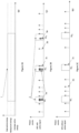
- Figures 1A-C show the emitted and received signals for a possible embodiment of the invention.
- Figure 1A shows a time lapse of the illumination by the light sources on a certain SPD, whereby a pulsing illumination pattern is maintained with square waves (1) with a fixed length and period, in which during every period the scene is actively illuminated by the light source for a time and is not actively illuminated by the light source for a time.
- Figure 1B shows detected events for an SPD, whereby every event (3a, 3b, 3c) shows an incidence of a photon on the SPD. Part of said events are the result of ambient light, random noise or error signals (3b, 3c), and a part of the events come from photons emitted by the light source (3a).
- the first group has a random distribution
- the second group will be in the time periods in which the light source emits light.
- Observation windows (2; W 1 , W 2 , W N ) are also visible in Figure 1B , in this case again with a fixed length and fixed period, for which the observation status of the SPD is registered (the possible detection of a photon incidence during the observation window).
- Figure 1C finally shows detected events (3b, 3c), without the events that are the result of illumination by the light sources, again with the observation windows indicated.
- Figures 2A-C show the same graphs, with the difference that, as is visible in Figure 2A , the light is not pulsed, but continuous.
- Figure 2B hereby only shows the events caused by the illumination in the observation windows.
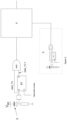
- Figure 3 shows a possible circuit for an SPD detector element according to the invention, whereby an (optional) coincidence condition is also imposed after the persistence condition via a circuit (4) to this end.
- the persistence condition is hereby imposed that two consecutive observation windows must show a positive observation status.
- a photon detector, SPD or SPAD, (5) is connected in series with a resistor across a voltage V BE , relative to the ground. In case of a photon incidence on the detector, this leads to a breakdown in the detector, and a current across the resistor (or in other words, a change of the voltage at the point between the detector and the resistor). Said circuit with resistor is referred to as "passive quenching”. It goes without saying that other "quenching" circuits such as “active quench” circuits are also applicable.
- a pulse detector which converts the measured voltage in a discrete signal (whereby 1 indicates a positive observation status, or therefore the detection of a photon incidence during the observation window; and 0 a negative observation status, or therefore the non-detection thereof).
- the signal that indicates the observation status of an observation window click_T n-1 is subsequently in fact provided with a delay via a flipflop (FF) according to the period of the observation windows (by clocking the FF with the rising edge of the observation window), and subsequently combined via an AND-port with the 'new', current signal which indicates the observation status as belonging to observation window click_T n . If both observation statuses are positive.
- the AND-port delivers a 1-confirmation signal at its output, which can then be used in the further processing of the signals, such as for example a combination with the signals from neighbouring detector elements (6).
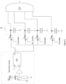
- Figure 5 shows a circuit where the past N observation statuses are kept in N memory elements (7).
- the circuit for determining the observation status leads the signal of the SPD (5) to the clock of the flipflop (FF), whereby the signal of the observation window works as data input (D) for the flipflop (FF), such that data output (Q) 1 is generated when the SPD detects a photon incidence in an observation window and a 0 in the absence thereof.
- the signal from the flipflop is saved in consecutive memory elements, whereby they are cyclically run through as storage.
- the memory elements provide the signal saved therein to a logical circuit which imposes the persistence conditions depending on their setting.
- the person skilled in the art can simply convert the conditions in a circuit using simple components, and they will not be discussed further here.
- an N input -AND port is provided, such that the persistence condition requires that in N of the past N observation windows a photon incidence must be detected to generate a confirmation signal (and then for example supplied further to a processing unit, which possibly imposes coincidence conditions).
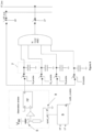
- Figure 6 shows a circuit where the circuit of Figure 5 is supplemented with a calibration circuit (9) which operates according to the routines discussed in the description.
- a High Priority (HP) or Low Priority (LP) is assigned to the SPD (5) in this case, the consequence being that in case of HP the observation status is not subjected to any further persistence condition, and immediately leads to a confirmation signal.
- HP High Priority
- LP Low Priority
- stricter persistence conditions are applied, in this case again the N positive observation statuses in the past N observation windows before a confirmation signal is generated.
- the SPD can also be switched off by the calibration routine if an issue is detected, (saturated SPD for example), via a switch (8).
- a coincidence condition is locally imposed on the confirmation signals before they are forwarded to further processing units.
- PCT/IB2021/054688 , BE2020/5975 and BE2021/5521 are referred to.
- the confirmation signals from the persistence circuit of Figure 6 are hereby processed by a coincidence circuit (10) before being forwarded to a suitable bus.
- Figure 8A shows a possible application of a circuit to impose a first possible calibration condition on an SPD (5) via a calibration circuit (9a), i.e. the absence of photon incidences over the past N calibration windows.
- the incoming 'click' signal indicates the possible detection of a photon incidence (detection signal), which is subsequently sent via an inverter to an OR-port, together with a signal that indicates whether the calibration routine is running. Said combination only results in a 0 if there is both a photon incidence (1 as detection signal) and the calibration routine is running (and the calibration condition is therefore not met in said calibration window).
- the output of the OR-port is delivered to a NAND-port, together with the inverted Q-output of a flipflop (FF).
- the output of the NAND-port goes to the data input D of the flipflop, which is clocked based on the start of each of the calibration windows.
- the signal delivered to the data input remains on 0, and the inverted Q output (QN) generates 1, which is looped back to the data input via the NAND-port and the "new" signal of the next calibration window, which therefore generates 1 as long as there is no photon incidence (as the 'click' is then 0, and inverted if 1 is delivered to the OR port, and therefore delivers a 1 to the NAND-port).
- the flipflop keeps repeating this loop. As soon as one photon incidence is detected, the flipflop generates a 0 as inverted output which via the inverted NAND-port always generates a 1, and thus again keeps looping an inverted output of 0.
- the resulting signal ZeroBG is subsequently used to classify the signal from the persistence routine as meeting the calibration condition or not, and thus can be used as HP or LP output, via the ports in the circuit of Figure 8B .
- Figure 9A shows a possibility to, in addition to the calibration circuit of Figure 8A , provide yet another second calibration circuit (9b), which further expands the possible classifications for an SPD (5).
- the calibration circuit (9a) of Figure 8A tries to determine which SPDs are not (or less) sensitive to background radiation (or thermal noise or the like)
- the second calibration circuit is aimed at determining whether saturated SPDs are present, which in other words will always indicate a detection.
- the signal from the AND-port is input for an OR-port, together with the looped data output Q of the flipflop (FF).
- the result from the OR-port is then the data input for the flipflop, with as clock signal that of the calibration windows.
- the resulting signal noSAT is subsequently used to classify the signal from the persistence routine as meeting the second calibration condition or not, and thus in the circuit of Figure 9B, together with the first calibration circuit of Figure 8A and the ensuing signal ZeroBG, to classify the SPDs and adjust the processing of the results.
- the presented circuit with a noSAT of 0 (saturated SPD) - and therefore also a ZeroBG of 0 - will always lead to the rejection of the signal from the SPD, even if it meets the persistence condition.
- ZeroBG determines whether the SPD is processed as high priority or low priority.
Landscapes
- Engineering & Computer Science (AREA)
- Multimedia (AREA)
- Signal Processing (AREA)
- Physics & Mathematics (AREA)
- General Physics & Mathematics (AREA)
- Spectroscopy & Molecular Physics (AREA)
- Computing Systems (AREA)
- Theoretical Computer Science (AREA)
- Photometry And Measurement Of Optical Pulse Characteristics (AREA)
- Optical Radar Systems And Details Thereof (AREA)
- Measurement Of The Respiration, Hearing Ability, Form, And Blood Characteristics Of Living Organisms (AREA)
- Transforming Light Signals Into Electric Signals (AREA)
Priority Applications (1)
| Application Number | Priority Date | Filing Date | Title |
|---|---|---|---|
| EP24188593.8A EP4471391A1 (en) | 2021-09-21 | 2022-09-13 | Persistence filtering in spd arrays |
Applications Claiming Priority (2)
| Application Number | Priority Date | Filing Date | Title |
|---|---|---|---|
| BE20215744A BE1029775B9 (nl) | 2021-09-21 | 2021-09-21 | Persistentiefiltering bij spd arrays |
| PCT/IB2022/058609 WO2023047245A1 (en) | 2021-09-21 | 2022-09-13 | Persistence filtering in spd arrays |
Related Child Applications (2)
| Application Number | Title | Priority Date | Filing Date |
|---|---|---|---|
| EP24188593.8A Division EP4471391A1 (en) | 2021-09-21 | 2022-09-13 | Persistence filtering in spd arrays |
| EP24188593.8A Division-Into EP4471391A1 (en) | 2021-09-21 | 2022-09-13 | Persistence filtering in spd arrays |
Publications (2)
| Publication Number | Publication Date |
|---|---|
| EP4241051A1 EP4241051A1 (en) | 2023-09-13 |
| EP4241051B1 true EP4241051B1 (en) | 2024-08-21 |
Family
ID=77914206
Family Applications (2)
| Application Number | Title | Priority Date | Filing Date |
|---|---|---|---|
| EP22777201.9A Active EP4241051B1 (en) | 2021-09-21 | 2022-09-13 | Persistence filtering in spd arrays |
| EP24188593.8A Pending EP4471391A1 (en) | 2021-09-21 | 2022-09-13 | Persistence filtering in spd arrays |
Family Applications After (1)
| Application Number | Title | Priority Date | Filing Date |
|---|---|---|---|
| EP24188593.8A Pending EP4471391A1 (en) | 2021-09-21 | 2022-09-13 | Persistence filtering in spd arrays |
Country Status (7)
| Country | Link |
|---|---|
| US (1) | US20240406582A1 (enExample) |
| EP (2) | EP4241051B1 (enExample) |
| JP (1) | JP2024534413A (enExample) |
| KR (1) | KR20240063146A (enExample) |
| CN (1) | CN117916563A (enExample) |
| BE (1) | BE1029775B9 (enExample) |
| WO (1) | WO2023047245A1 (enExample) |
Families Citing this family (7)
| Publication number | Priority date | Publication date | Assignee | Title |
|---|---|---|---|---|
| EP4534951A1 (en) * | 2023-10-06 | 2025-04-09 | VoxelSensors SRL | Depth sensing system and method |
| WO2025176834A1 (en) | 2024-02-22 | 2025-08-28 | Voxelsensors Srl | Optical sensing system |
| EP4671816A1 (en) | 2024-06-27 | 2025-12-31 | VoxelSensors SRL | OPTICAL DETECTION SYSTEM |
| WO2025261994A1 (en) | 2024-06-17 | 2025-12-26 | Voxelsensors Srl | System and method for visual awareness |
| EP4749401A1 (en) | 2024-11-20 | 2026-05-27 | VoxelSensors SRL | System and method for visual awareness |
| EP4718143A1 (en) | 2024-09-26 | 2026-04-01 | VoxelSensors SRL | Projector and method of projection |
| WO2025262029A1 (en) | 2024-06-18 | 2025-12-26 | Voxelsensors Srl | Projector and method of projection |
Family Cites Families (8)
| Publication number | Priority date | Publication date | Assignee | Title |
|---|---|---|---|---|
| US20150097951A1 (en) * | 2013-07-17 | 2015-04-09 | Geoffrey Louis Barrows | Apparatus for Vision in Low Light Environments |
| EP3159711A1 (en) * | 2015-10-23 | 2017-04-26 | Xenomatix NV | System and method for determining a distance to an object |
| CN110537124B (zh) * | 2017-03-01 | 2021-12-07 | 奥斯特公司 | 用于lidar的准确光检测器测量 |
| EP3688809B1 (en) * | 2017-09-27 | 2025-08-20 | The Commonwealth of Australia | A neuromorphic single photon avalanche detector (spad) array microchip |
| WO2019093208A1 (ja) * | 2017-11-07 | 2019-05-16 | 江藤 剛治 | 高速イメージセンサ |
| US10497738B2 (en) * | 2018-04-20 | 2019-12-03 | Omnivision Technologies, Inc. | First photon correlated time-of-flight sensor |
| KR102747641B1 (ko) * | 2019-06-26 | 2024-12-27 | 삼성전자주식회사 | 비전 센서, 이를 포함하는 이미지 처리 장치 및 비전 센서의 동작 방법 |
| WO2021054688A1 (ko) | 2019-09-19 | 2021-03-25 | 한양대학교 산학협력단 | 온도감응형 자성중심 덴드리머 및 이의 제조방법 |
-
2021
- 2021-09-21 BE BE20215744A patent/BE1029775B9/nl active IP Right Grant
-
2022
- 2022-09-13 EP EP22777201.9A patent/EP4241051B1/en active Active
- 2022-09-13 CN CN202280060751.5A patent/CN117916563A/zh active Pending
- 2022-09-13 WO PCT/IB2022/058609 patent/WO2023047245A1/en not_active Ceased
- 2022-09-13 EP EP24188593.8A patent/EP4471391A1/en active Pending
- 2022-09-13 KR KR1020247012321A patent/KR20240063146A/ko active Pending
- 2022-09-13 US US18/692,300 patent/US20240406582A1/en active Pending
- 2022-09-13 JP JP2024516747A patent/JP2024534413A/ja active Pending
Also Published As
| Publication number | Publication date |
|---|---|
| JP2024534413A (ja) | 2024-09-20 |
| US20240406582A1 (en) | 2024-12-05 |
| EP4241051A1 (en) | 2023-09-13 |
| EP4471391A1 (en) | 2024-12-04 |
| BE1029775B1 (nl) | 2023-04-17 |
| KR20240063146A (ko) | 2024-05-09 |
| BE1029775A1 (nl) | 2023-04-13 |
| WO2023047245A1 (en) | 2023-03-30 |
| BE1029775B9 (nl) | 2023-10-09 |
| BE1029775A9 (nl) | 2023-10-02 |
| CN117916563A (zh) | 2024-04-19 |
Similar Documents
| Publication | Publication Date | Title |
|---|---|---|
| EP4471391A1 (en) | Persistence filtering in spd arrays | |
| US20250119666A1 (en) | Pixel sensor system | |
| JP7541030B2 (ja) | Lidarシステムにおける時間的ジッタ | |
| CN105043539B (zh) | 用于运行光电探测器的方法和装置 | |
| US12593146B2 (en) | Pixel array with dynamic lateral and temporal resolution | |
| JP2024534413A5 (enExample) | ||
| US20200066779A1 (en) | Pixel circuit and method of operating the same in an always-on mode | |
| KR102886690B1 (ko) | 인접-게이트 스위칭 픽셀 센서 | |
| US20230194711A1 (en) | LIDAR Device, System and Method | |
| US11644553B2 (en) | Detection of reflected light pulses in the presence of ambient light | |
| JPH0758387A (ja) | 変調レーザ信号を検出する装置 | |
| CN113711080B (zh) | 激光雷达的探测方法、计算机可读存储介质和激光雷达 | |
| JPWO2019050024A1 (ja) | 距離測定方法および距離測定装置 | |
| US12546862B2 (en) | Apparatus for generating backscatter histogram data for determining a diffuse backscatter during an optical runtime measurement and a method | |
| US5404162A (en) | Method to image high speed events | |
| BE1028366B1 (nl) | Pixel sensor systeem | |
| US20250189638A1 (en) | Time-of-flight system and method | |
| BE1028950B9 (nl) | Buurtgebonden geschakelde pixel-sensor | |
| JP2515136B2 (ja) | 反射形光電検出装置 | |
| JP2025537174A (ja) | 光学センシングシステム | |
| CN121577169A (zh) | 一种暗计数与光脉冲的自适应区分装置及方法 |
Legal Events
| Date | Code | Title | Description |
|---|---|---|---|
| STAA | Information on the status of an ep patent application or granted ep patent |
Free format text: STATUS: UNKNOWN |
|
| STAA | Information on the status of an ep patent application or granted ep patent |
Free format text: STATUS: THE INTERNATIONAL PUBLICATION HAS BEEN MADE |
|
| PUAI | Public reference made under article 153(3) epc to a published international application that has entered the european phase |
Free format text: ORIGINAL CODE: 0009012 |
|
| STAA | Information on the status of an ep patent application or granted ep patent |
Free format text: STATUS: REQUEST FOR EXAMINATION WAS MADE |
|
| 17P | Request for examination filed |
Effective date: 20230606 |
|
| AK | Designated contracting states |
Kind code of ref document: A1 Designated state(s): AL AT BE BG CH CY CZ DE DK EE ES FI FR GB GR HR HU IE IS IT LI LT LU LV MC MK MT NL NO PL PT RO RS SE SI SK SM TR |
|
| STAA | Information on the status of an ep patent application or granted ep patent |
Free format text: STATUS: EXAMINATION IS IN PROGRESS |
|
| 17Q | First examination report despatched |
Effective date: 20240108 |
|
| GRAP | Despatch of communication of intention to grant a patent |
Free format text: ORIGINAL CODE: EPIDOSNIGR1 |
|
| STAA | Information on the status of an ep patent application or granted ep patent |
Free format text: STATUS: GRANT OF PATENT IS INTENDED |
|
| DAV | Request for validation of the european patent (deleted) | ||
| DAX | Request for extension of the european patent (deleted) | ||
| GRAS | Grant fee paid |
Free format text: ORIGINAL CODE: EPIDOSNIGR3 |
|
| INTG | Intention to grant announced |
Effective date: 20240621 |
|
| GRAA | (expected) grant |
Free format text: ORIGINAL CODE: 0009210 |
|
| STAA | Information on the status of an ep patent application or granted ep patent |
Free format text: STATUS: THE PATENT HAS BEEN GRANTED |
|
| AK | Designated contracting states |
Kind code of ref document: B1 Designated state(s): AL AT BE BG CH CY CZ DE DK EE ES FI FR GB GR HR HU IE IS IT LI LT LU LV MC MK MT NL NO PL PT RO RS SE SI SK SM TR |
|
| REG | Reference to a national code |
Ref country code: GB Ref legal event code: FG4D |
|
| REG | Reference to a national code |
Ref country code: CH Ref legal event code: EP |
|
| REG | Reference to a national code |
Ref country code: IE Ref legal event code: FG4D |
|
| REG | Reference to a national code |
Ref country code: DE Ref legal event code: R096 Ref document number: 602022005537 Country of ref document: DE |
|
| REG | Reference to a national code |
Ref country code: LT Ref legal event code: MG9D |
|
| REG | Reference to a national code |
Ref country code: NL Ref legal event code: MP Effective date: 20240821 |
|
| PG25 | Lapsed in a contracting state [announced via postgrant information from national office to epo] |
Ref country code: NO Free format text: LAPSE BECAUSE OF FAILURE TO SUBMIT A TRANSLATION OF THE DESCRIPTION OR TO PAY THE FEE WITHIN THE PRESCRIBED TIME-LIMIT Effective date: 20241121 |
|
| REG | Reference to a national code |
Ref country code: AT Ref legal event code: MK05 Ref document number: 1715910 Country of ref document: AT Kind code of ref document: T Effective date: 20240821 |
|
| PG25 | Lapsed in a contracting state [announced via postgrant information from national office to epo] |
Ref country code: FI Free format text: LAPSE BECAUSE OF FAILURE TO SUBMIT A TRANSLATION OF THE DESCRIPTION OR TO PAY THE FEE WITHIN THE PRESCRIBED TIME-LIMIT Effective date: 20240821 Ref country code: GR Free format text: LAPSE BECAUSE OF FAILURE TO SUBMIT A TRANSLATION OF THE DESCRIPTION OR TO PAY THE FEE WITHIN THE PRESCRIBED TIME-LIMIT Effective date: 20241122 Ref country code: PT Free format text: LAPSE BECAUSE OF FAILURE TO SUBMIT A TRANSLATION OF THE DESCRIPTION OR TO PAY THE FEE WITHIN THE PRESCRIBED TIME-LIMIT Effective date: 20241223 Ref country code: PL Free format text: LAPSE BECAUSE OF FAILURE TO SUBMIT A TRANSLATION OF THE DESCRIPTION OR TO PAY THE FEE WITHIN THE PRESCRIBED TIME-LIMIT Effective date: 20240821 Ref country code: NL Free format text: LAPSE BECAUSE OF FAILURE TO SUBMIT A TRANSLATION OF THE DESCRIPTION OR TO PAY THE FEE WITHIN THE PRESCRIBED TIME-LIMIT Effective date: 20240821 |
|
| PG25 | Lapsed in a contracting state [announced via postgrant information from national office to epo] |
Ref country code: BG Free format text: LAPSE BECAUSE OF FAILURE TO SUBMIT A TRANSLATION OF THE DESCRIPTION OR TO PAY THE FEE WITHIN THE PRESCRIBED TIME-LIMIT Effective date: 20240821 |
|
| PG25 | Lapsed in a contracting state [announced via postgrant information from national office to epo] |
Ref country code: LV Free format text: LAPSE BECAUSE OF FAILURE TO SUBMIT A TRANSLATION OF THE DESCRIPTION OR TO PAY THE FEE WITHIN THE PRESCRIBED TIME-LIMIT Effective date: 20240821 |
|
| PG25 | Lapsed in a contracting state [announced via postgrant information from national office to epo] |
Ref country code: IS Free format text: LAPSE BECAUSE OF FAILURE TO SUBMIT A TRANSLATION OF THE DESCRIPTION OR TO PAY THE FEE WITHIN THE PRESCRIBED TIME-LIMIT Effective date: 20241221 Ref country code: AT Free format text: LAPSE BECAUSE OF FAILURE TO SUBMIT A TRANSLATION OF THE DESCRIPTION OR TO PAY THE FEE WITHIN THE PRESCRIBED TIME-LIMIT Effective date: 20240821 |
|
| PG25 | Lapsed in a contracting state [announced via postgrant information from national office to epo] |
Ref country code: HR Free format text: LAPSE BECAUSE OF FAILURE TO SUBMIT A TRANSLATION OF THE DESCRIPTION OR TO PAY THE FEE WITHIN THE PRESCRIBED TIME-LIMIT Effective date: 20240821 |
|
| PG25 | Lapsed in a contracting state [announced via postgrant information from national office to epo] |
Ref country code: ES Free format text: LAPSE BECAUSE OF FAILURE TO SUBMIT A TRANSLATION OF THE DESCRIPTION OR TO PAY THE FEE WITHIN THE PRESCRIBED TIME-LIMIT Effective date: 20240821 Ref country code: RS Free format text: LAPSE BECAUSE OF FAILURE TO SUBMIT A TRANSLATION OF THE DESCRIPTION OR TO PAY THE FEE WITHIN THE PRESCRIBED TIME-LIMIT Effective date: 20241121 |
|
| PG25 | Lapsed in a contracting state [announced via postgrant information from national office to epo] |
Ref country code: RS Free format text: LAPSE BECAUSE OF FAILURE TO SUBMIT A TRANSLATION OF THE DESCRIPTION OR TO PAY THE FEE WITHIN THE PRESCRIBED TIME-LIMIT Effective date: 20241121 Ref country code: PT Free format text: LAPSE BECAUSE OF FAILURE TO SUBMIT A TRANSLATION OF THE DESCRIPTION OR TO PAY THE FEE WITHIN THE PRESCRIBED TIME-LIMIT Effective date: 20241223 Ref country code: PL Free format text: LAPSE BECAUSE OF FAILURE TO SUBMIT A TRANSLATION OF THE DESCRIPTION OR TO PAY THE FEE WITHIN THE PRESCRIBED TIME-LIMIT Effective date: 20240821 Ref country code: NO Free format text: LAPSE BECAUSE OF FAILURE TO SUBMIT A TRANSLATION OF THE DESCRIPTION OR TO PAY THE FEE WITHIN THE PRESCRIBED TIME-LIMIT Effective date: 20241121 Ref country code: NL Free format text: LAPSE BECAUSE OF FAILURE TO SUBMIT A TRANSLATION OF THE DESCRIPTION OR TO PAY THE FEE WITHIN THE PRESCRIBED TIME-LIMIT Effective date: 20240821 Ref country code: LV Free format text: LAPSE BECAUSE OF FAILURE TO SUBMIT A TRANSLATION OF THE DESCRIPTION OR TO PAY THE FEE WITHIN THE PRESCRIBED TIME-LIMIT Effective date: 20240821 Ref country code: IS Free format text: LAPSE BECAUSE OF FAILURE TO SUBMIT A TRANSLATION OF THE DESCRIPTION OR TO PAY THE FEE WITHIN THE PRESCRIBED TIME-LIMIT Effective date: 20241221 Ref country code: HR Free format text: LAPSE BECAUSE OF FAILURE TO SUBMIT A TRANSLATION OF THE DESCRIPTION OR TO PAY THE FEE WITHIN THE PRESCRIBED TIME-LIMIT Effective date: 20240821 Ref country code: GR Free format text: LAPSE BECAUSE OF FAILURE TO SUBMIT A TRANSLATION OF THE DESCRIPTION OR TO PAY THE FEE WITHIN THE PRESCRIBED TIME-LIMIT Effective date: 20241122 Ref country code: FI Free format text: LAPSE BECAUSE OF FAILURE TO SUBMIT A TRANSLATION OF THE DESCRIPTION OR TO PAY THE FEE WITHIN THE PRESCRIBED TIME-LIMIT Effective date: 20240821 Ref country code: ES Free format text: LAPSE BECAUSE OF FAILURE TO SUBMIT A TRANSLATION OF THE DESCRIPTION OR TO PAY THE FEE WITHIN THE PRESCRIBED TIME-LIMIT Effective date: 20240821 Ref country code: BG Free format text: LAPSE BECAUSE OF FAILURE TO SUBMIT A TRANSLATION OF THE DESCRIPTION OR TO PAY THE FEE WITHIN THE PRESCRIBED TIME-LIMIT Effective date: 20240821 Ref country code: AT Free format text: LAPSE BECAUSE OF FAILURE TO SUBMIT A TRANSLATION OF THE DESCRIPTION OR TO PAY THE FEE WITHIN THE PRESCRIBED TIME-LIMIT Effective date: 20240821 |
|
| P01 | Opt-out of the competence of the unified patent court (upc) registered |
Free format text: CASE NUMBER: APP_7200/2025 Effective date: 20250212 |
|
| PG25 | Lapsed in a contracting state [announced via postgrant information from national office to epo] |
Ref country code: RO Free format text: LAPSE BECAUSE OF FAILURE TO SUBMIT A TRANSLATION OF THE DESCRIPTION OR TO PAY THE FEE WITHIN THE PRESCRIBED TIME-LIMIT Effective date: 20240821 Ref country code: DK Free format text: LAPSE BECAUSE OF FAILURE TO SUBMIT A TRANSLATION OF THE DESCRIPTION OR TO PAY THE FEE WITHIN THE PRESCRIBED TIME-LIMIT Effective date: 20240821 Ref country code: SM Free format text: LAPSE BECAUSE OF FAILURE TO SUBMIT A TRANSLATION OF THE DESCRIPTION OR TO PAY THE FEE WITHIN THE PRESCRIBED TIME-LIMIT Effective date: 20240821 |
|
| PG25 | Lapsed in a contracting state [announced via postgrant information from national office to epo] |
Ref country code: EE Free format text: LAPSE BECAUSE OF FAILURE TO SUBMIT A TRANSLATION OF THE DESCRIPTION OR TO PAY THE FEE WITHIN THE PRESCRIBED TIME-LIMIT Effective date: 20240821 |
|
| PG25 | Lapsed in a contracting state [announced via postgrant information from national office to epo] |
Ref country code: CZ Free format text: LAPSE BECAUSE OF FAILURE TO SUBMIT A TRANSLATION OF THE DESCRIPTION OR TO PAY THE FEE WITHIN THE PRESCRIBED TIME-LIMIT Effective date: 20240821 |
|
| PG25 | Lapsed in a contracting state [announced via postgrant information from national office to epo] |
Ref country code: SK Free format text: LAPSE BECAUSE OF FAILURE TO SUBMIT A TRANSLATION OF THE DESCRIPTION OR TO PAY THE FEE WITHIN THE PRESCRIBED TIME-LIMIT Effective date: 20240821 |
|
| PG25 | Lapsed in a contracting state [announced via postgrant information from national office to epo] |
Ref country code: LU Free format text: LAPSE BECAUSE OF NON-PAYMENT OF DUE FEES Effective date: 20240913 |
|
| REG | Reference to a national code |
Ref country code: DE Ref legal event code: R097 Ref document number: 602022005537 Country of ref document: DE |
|
| PLBE | No opposition filed within time limit |
Free format text: ORIGINAL CODE: 0009261 |
|
| STAA | Information on the status of an ep patent application or granted ep patent |
Free format text: STATUS: NO OPPOSITION FILED WITHIN TIME LIMIT |
|
| PG25 | Lapsed in a contracting state [announced via postgrant information from national office to epo] |
Ref country code: MC Free format text: LAPSE BECAUSE OF FAILURE TO SUBMIT A TRANSLATION OF THE DESCRIPTION OR TO PAY THE FEE WITHIN THE PRESCRIBED TIME-LIMIT Effective date: 20240821 |
|
| REG | Reference to a national code |
Ref country code: BE Ref legal event code: MM Effective date: 20240930 |
|
| PG25 | Lapsed in a contracting state [announced via postgrant information from national office to epo] |
Ref country code: BE Free format text: LAPSE BECAUSE OF NON-PAYMENT OF DUE FEES Effective date: 20240930 |
|
| PG25 | Lapsed in a contracting state [announced via postgrant information from national office to epo] |
Ref country code: IE Free format text: LAPSE BECAUSE OF NON-PAYMENT OF DUE FEES Effective date: 20240913 |
|
| 26N | No opposition filed |
Effective date: 20250522 |
|
| PG25 | Lapsed in a contracting state [announced via postgrant information from national office to epo] |
Ref country code: SE Free format text: LAPSE BECAUSE OF FAILURE TO SUBMIT A TRANSLATION OF THE DESCRIPTION OR TO PAY THE FEE WITHIN THE PRESCRIBED TIME-LIMIT Effective date: 20240821 |
|
| PGFP | Annual fee paid to national office [announced via postgrant information from national office to epo] |
Ref country code: DE Payment date: 20250312 Year of fee payment: 4 |
|
| PGFP | Annual fee paid to national office [announced via postgrant information from national office to epo] |
Ref country code: IT Payment date: 20250930 Year of fee payment: 4 |
|
| PG25 | Lapsed in a contracting state [announced via postgrant information from national office to epo] |
Ref country code: CY Free format text: LAPSE BECAUSE OF FAILURE TO SUBMIT A TRANSLATION OF THE DESCRIPTION OR TO PAY THE FEE WITHIN THE PRESCRIBED TIME-LIMIT; INVALID AB INITIO Effective date: 20220913 |
|
| PG25 | Lapsed in a contracting state [announced via postgrant information from national office to epo] |
Ref country code: HU Free format text: LAPSE BECAUSE OF FAILURE TO SUBMIT A TRANSLATION OF THE DESCRIPTION OR TO PAY THE FEE WITHIN THE PRESCRIBED TIME-LIMIT; INVALID AB INITIO Effective date: 20220913 |
|
| REG | Reference to a national code |
Ref country code: CH Ref legal event code: H13 Free format text: ST27 STATUS EVENT CODE: U-0-0-H10-H13 (AS PROVIDED BY THE NATIONAL OFFICE) Effective date: 20260504 |
|
| PG25 | Lapsed in a contracting state [announced via postgrant information from national office to epo] |
Ref country code: TR Free format text: LAPSE BECAUSE OF FAILURE TO SUBMIT A TRANSLATION OF THE DESCRIPTION OR TO PAY THE FEE WITHIN THE PRESCRIBED TIME-LIMIT Effective date: 20240821 |
|
| PG25 | Lapsed in a contracting state [announced via postgrant information from national office to epo] |
Ref country code: SI Free format text: LAPSE BECAUSE OF FAILURE TO SUBMIT A TRANSLATION OF THE DESCRIPTION OR TO PAY THE FEE WITHIN THE PRESCRIBED TIME-LIMIT Effective date: 20240821 |
|
| PG25 | Lapsed in a contracting state [announced via postgrant information from national office to epo] |
Ref country code: LT Free format text: LAPSE BECAUSE OF FAILURE TO SUBMIT A TRANSLATION OF THE DESCRIPTION OR TO PAY THE FEE WITHIN THE PRESCRIBED TIME-LIMIT Effective date: 20240821 |
|
| PG25 | Lapsed in a contracting state [announced via postgrant information from national office to epo] |
Ref country code: CH Free format text: LAPSE BECAUSE OF NON-PAYMENT OF DUE FEES Effective date: 20250930 |
|
| PGFP | Annual fee paid to national office [announced via postgrant information from national office to epo] |
Ref country code: FR Payment date: 20260526 Year of fee payment: 5 |