EP4239983A1 - Motor aus einer formgedächtnislegierung, motormodul, kameramodul, elektronische vorrichtung - Google Patents
Motor aus einer formgedächtnislegierung, motormodul, kameramodul, elektronische vorrichtung Download PDFInfo
- Publication number
- EP4239983A1 EP4239983A1 EP21897114.1A EP21897114A EP4239983A1 EP 4239983 A1 EP4239983 A1 EP 4239983A1 EP 21897114 A EP21897114 A EP 21897114A EP 4239983 A1 EP4239983 A1 EP 4239983A1
- Authority
- EP
- European Patent Office
- Prior art keywords
- magnetic isolation
- sma
- magnetic
- motor
- isolation member
- Prior art date
- Legal status (The legal status is an assumption and is not a legal conclusion. Google has not performed a legal analysis and makes no representation as to the accuracy of the status listed.)
- Granted
Links
Images


Classifications
-
- G—PHYSICS
- G02—OPTICS
- G02B—OPTICAL ELEMENTS, SYSTEMS OR APPARATUS
- G02B27/00—Optical systems or apparatus not provided for by any of the groups G02B1/00 - G02B26/00, G02B30/00
- G02B27/64—Imaging systems using optical elements for stabilisation of the lateral and angular position of the image
- G02B27/646—Imaging systems using optical elements for stabilisation of the lateral and angular position of the image compensating for small deviations, e.g. due to vibration or shake
-
- G—PHYSICS
- G02—OPTICS
- G02B—OPTICAL ELEMENTS, SYSTEMS OR APPARATUS
- G02B7/00—Mountings, adjusting means, or light-tight connections, for optical elements
- G02B7/02—Mountings, adjusting means, or light-tight connections, for optical elements for lenses
- G02B7/04—Mountings, adjusting means, or light-tight connections, for optical elements for lenses with mechanism for focusing or varying magnification
- G02B7/08—Mountings, adjusting means, or light-tight connections, for optical elements for lenses with mechanism for focusing or varying magnification adapted to co-operate with a remote control mechanism
-
- G—PHYSICS
- G03—PHOTOGRAPHY; CINEMATOGRAPHY; ANALOGOUS TECHNIQUES USING WAVES OTHER THAN OPTICAL WAVES; ELECTROGRAPHY; HOLOGRAPHY
- G03B—APPARATUS OR ARRANGEMENTS FOR TAKING PHOTOGRAPHS OR FOR PROJECTING OR VIEWING THEM; APPARATUS OR ARRANGEMENTS EMPLOYING ANALOGOUS TECHNIQUES USING WAVES OTHER THAN OPTICAL WAVES; ACCESSORIES THEREFOR
- G03B30/00—Camera modules comprising integrated lens units and imaging units, specially adapted for being embedded in other devices, e.g. mobile phones or vehicles
-
- H—ELECTRICITY
- H04—ELECTRIC COMMUNICATION TECHNIQUE
- H04M—TELEPHONIC COMMUNICATION
- H04M1/00—Substation equipment, e.g. for use by subscribers
- H04M1/02—Constructional features of telephone sets
- H04M1/0202—Portable telephone sets, e.g. cordless phones, mobile phones or bar type handsets
- H04M1/026—Details of the structure or mounting of specific components
-
- H—ELECTRICITY
- H04—ELECTRIC COMMUNICATION TECHNIQUE
- H04N—PICTORIAL COMMUNICATION, e.g. TELEVISION
- H04N23/00—Cameras or camera modules comprising electronic image sensors; Control thereof
- H04N23/50—Constructional details
- H04N23/52—Elements optimising image sensor operation, e.g. for electromagnetic interference [EMI] protection or temperature control by heat transfer or cooling elements
-
- H—ELECTRICITY
- H04—ELECTRIC COMMUNICATION TECHNIQUE
- H04N—PICTORIAL COMMUNICATION, e.g. TELEVISION
- H04N23/00—Cameras or camera modules comprising electronic image sensors; Control thereof
- H04N23/50—Constructional details
- H04N23/54—Mounting of pick-up tubes, electronic image sensors, deviation or focusing coils
-
- H—ELECTRICITY
- H04—ELECTRIC COMMUNICATION TECHNIQUE
- H04N—PICTORIAL COMMUNICATION, e.g. TELEVISION
- H04N23/00—Cameras or camera modules comprising electronic image sensors; Control thereof
- H04N23/50—Constructional details
- H04N23/55—Optical parts specially adapted for electronic image sensors; Mounting thereof
-
- H—ELECTRICITY
- H04—ELECTRIC COMMUNICATION TECHNIQUE
- H04N—PICTORIAL COMMUNICATION, e.g. TELEVISION
- H04N23/00—Cameras or camera modules comprising electronic image sensors; Control thereof
- H04N23/57—Mechanical or electrical details of cameras or camera modules specially adapted for being embedded in other devices
-
- H—ELECTRICITY
- H04—ELECTRIC COMMUNICATION TECHNIQUE
- H04N—PICTORIAL COMMUNICATION, e.g. TELEVISION
- H04N25/00—Circuitry of solid-state image sensors [SSIS]; Control thereof
- H04N25/60—Noise processing, e.g. detecting, correcting, reducing or removing noise
- H04N25/617—Noise processing, e.g. detecting, correcting, reducing or removing noise for reducing electromagnetic interference, e.g. clocking noise
-
- G—PHYSICS
- G03—PHOTOGRAPHY; CINEMATOGRAPHY; ANALOGOUS TECHNIQUES USING WAVES OTHER THAN OPTICAL WAVES; ELECTROGRAPHY; HOLOGRAPHY
- G03B—APPARATUS OR ARRANGEMENTS FOR TAKING PHOTOGRAPHS OR FOR PROJECTING OR VIEWING THEM; APPARATUS OR ARRANGEMENTS EMPLOYING ANALOGOUS TECHNIQUES USING WAVES OTHER THAN OPTICAL WAVES; ACCESSORIES THEREFOR
- G03B2205/00—Adjustment of optical system relative to image or object surface other than for focusing
- G03B2205/0053—Driving means for the movement of one or more optical element
- G03B2205/0076—Driving means for the movement of one or more optical element using shape memory alloys
-
- H—ELECTRICITY
- H04—ELECTRIC COMMUNICATION TECHNIQUE
- H04M—TELEPHONIC COMMUNICATION
- H04M1/00—Substation equipment, e.g. for use by subscribers
- H04M1/02—Constructional features of telephone sets
- H04M1/0202—Portable telephone sets, e.g. cordless phones, mobile phones or bar type handsets
- H04M1/026—Details of the structure or mounting of specific components
- H04M1/0264—Details of the structure or mounting of specific components for a camera module assembly
Definitions
- This application relates to the field of electronic devices, and more specifically, to a shape memory alloy motor, a motor module, a camera compact module, and an electronic device.
- the first magnetic isolation member is disposed between the image sensor and the SMA motor, thereby being conducive to reducing magnetic interference to a magnetic sensitive electronic component in the camera compact module.
- an interference magnetic field generated by the SMA motor may be smaller at the first magnetic isolation member, thereby being conducive to further reducing a degree of the magnetic interference to the magnetic sensitive electronic component in the camera compact module.
- the second magnetic isolation member may be closer to the lens array
- the first magnetic isolation member may be closer to the image sensor
- a distance between the second magnetic isolation member and the first magnetic isolation member may be larger
- the interference magnetic field generated by the SMA motor may be smaller at the first magnetic isolation member, thereby being conducive to further reducing the magnetic interference to the magnetic sensitive electronic component in the camera compact module.
- a magnetic isolation edge is disposed on the second magnetic isolation member, so that a magnetic isolation region of the second magnetic isolation member is increased, and a magnetic isolation effect may also be implemented in a direction perpendicular to the second magnetic isolation board, thereby being conducive to further reducing the magnetic interference to the magnetic sensitive electronic component in the camera compact module.
- an inner wall of the second magnetic isolation edge is in communication with a hole wall of the second through hole.
- the magnetic isolation edge is disposed at a position of the magnetic sensitive electronic component, thereby being conducive to improving a magnetic isolation effect of the second magnetic isolation member and further reducing the degree of the magnetic interference to the magnetic sensitive electronic component in the camera compact module.
- distribution of the second magnetic isolation edge is flexibly arranged, thereby being conducive to flexibly adjusting the magnetic isolation effect of the second magnetic isolation member.
- the second magnetic isolation member satisfies at least one of the following:
- the relative magnetic permeability of the second magnetic isolation member is greater than 5.
- the first magnetic isolation member includes:
- the camera compact module satisfies at least one of the following:
- a structure and performance of the first magnetic isolation member are disposed, thereby being conducive to improving the magnetic isolation effect of the first magnetic isolation member and further reducing the magnetic interference to the magnetic sensitive electronic component in the camera compact module.
- the camera compact module further includes: a holder, where the holder is located between the image sensor and the SMA motor, and the first magnetic isolation member is located in the holder or is attached to a surface of the holder.
- a disposition position of the first magnetic isolation member relative to the holder is flexibly arranged, thereby being conducive to improving integration of the camera compact module.
- it is conducive to ensuring that a specific distance exists between the first magnetic isolation member and the image sensor, thereby reducing impact of an interference magnetic field generated by the first magnetic isolation member on the image sensor.
- the second magnetic isolation member may be closer to the lens array, the second magnetic isolation member may be relatively away from the image sensor, thereby being conducive to ensuring that a specific distance exists between the second magnetic isolation member and the image sensor and further reducing impact of an interference magnetic field generated by the second magnetic isolation member on the image sensor.
- the at least one second magnetic isolation edge includes a target second magnetic isolation edge, and the target second magnetic isolation edge and a pin of the image sensor are located on a same side of the camera compact module.
- the relative magnetic permeability of the second magnetic isolation member is greater than 5.
- the second magnetic isolation member includes:
- the second magnetic isolation board satisfies at least one of the following:
- an inner wall of the first magnetic isolation edge is in communication with a hole wall of the first through hole.
- the relative magnetic permeability of the first magnetic isolation member is greater than 5.
- the SMA motor further includes: a holder, where the first magnetic isolation member is located in the holder or is attached to a surface of the holder.
- an electronic device including the motor module according to any possible implementation of the third aspect to the fourth aspect.
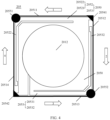
- a rear-facing camera compact module 120 may be disposed on the rear cover 20 of the electronic device 100. As shown in a right figure in FIG. 1 , the rear-facing camera compact module 120 may be installed at an upper left part of the rear cover 20. The rear-facing camera compact module 120 may be configured to, for example, photograph a scene around the electronic device 100.
- the motor module 202 may include a lens array 2022, a voice coil motor (voice coil motor, VCM) 204, a shape memory alloy (shape memory alloy, SMA) motor 205, and a lens tube (not shown in FIG. 2 ) configured to accommodate the lens array 2022, the voice coil motor 204, and the SMA motor 205.
- VCM voice coil motor
- SMA shape memory alloy
- the circuit board 203 may include a driver module (not shown in FIG. 2 ).
- the driver module may supply power to various electronic components (such as the voice coil motor 204, the SMA motor 205, and the image sensor 207) in the camera compact module 200.
- the driver module may include, for example, an SMA motor driver module (the SMA motor driver module is used as an example below for description).
- the circuit board 203 may further transmit a signal from an electronic component in the camera compact module 200 to the outside of the camera compact module 200.
- the image sensor 207 may be disposed on the circuit board 203. A center of the image sensor 207 may be aligned with an optical axis of the lens array 2022.
- the lens array 2022 may pass through the through hole 2011 on the camera housing 201 and extend out of the camera housing 201.
- the lens array 2022 may project light of a periphery of the camera housing 201 onto the image sensor 207.
- the lens array 2022 may further move or rotate in the through hole 2011, to implement functions such as auto focus (auto focus) and optical image stabilization (optical image stabilization, OIS).
- the voice coil motor 204 may be configured to perform the auto focus function. As shown in FIG. 3 , the voice coil motor 204 may include a magnet 2041 and a coil 2042 that are disposed around the lens array 2022.
- the magnet 2041 may be fixed in the camera housing 201 and be still relative to the camera housing 201, and the coil 2042 may be fixed on the lens array 2022.
- the circuit board 203 may supply power to the coil 2042.
- the powered coil 2042 may generate a magnetic field 1.
- the magnetic field 1 interacts with a magnetic field 2 generated by the magnet 2041, so that an attractive force or a repulsive force may be generated. Therefore, the coil 2042 may drive the lens array 2022 to move under an action of the attractive force or the repulsive force, to implement the auto focus function.
- an insufficient driving force of the voice coil motor 204 is not conducive to photographing a high-quality image, for example, the image may be blurred. If the driving force of the voice coil motor 204 is enhanced, a volume of the voice coil motor 204 needs to be increased, which is not conducive to miniaturization of the camera compact module 200.
- the SMA motor 205 may further include a rotor end 20541 and a rotor end 20542 that are connected to the lens array 2022, and a stator end 20551 and a stator end 20552 that are fixed relative to the camera housing 201.
- the SMA motor 205 may further include a spring plate 2050, and the spring plate 2050 may be connected to the rotor end 20541 and the rotor end 20542.
- the spring plate 2050 may further include a spring plate arm 2052 and a spring plate arm 2053. A tail end of the spring plate arm 2052 is close to the rotor end 20541, and an open end of the spring plate arm 2052 extends to the rotor end 20542.
- the spring plate arm 2052 may include a spring plate arm section 20521 disposed close to the SMA cable 20511 and in parallel with the SMA cable 20511.
- the spring plate arm 2052 may further include a spring plate arm section 20522 disposed close to the SMA cable 20514 and in parallel with the SMA cable 20514. Similarly, a tail end of the spring plate arm 2053 is close to the rotor end 20542, and an open end of the spring plate arm 2052 extends to the rotor end 20541 .
- the spring plate arm 2053 may include a spring plate arm section 20531 disposed close to the SMA cable 20513 and in parallel with the SMA cable 20513.
- the spring plate arm 2053 may further include a spring plate arm section 20532 disposed close to the SMA cable 20512 and in parallel with the SMA cable 20512.
- the SMA motor driver module may include a first electrical connection port 1 and a second electrical connection port 1 that correspond to the SMA cable 20511, may further include a first electrical connection port 2 and a second electrical connection port 2 that correspond to the SMA cable 20512, may further include a first electrical connection port 3 and a second electrical connection port 3 that correspond to the SMA cable 20513, and may further include a first electrical connection port 4 and a second electrical connection port 4 that correspond to the SMA cable 20514.
- Two ends of the SMA cable 20511 may be electrically connected to the first electrical connection port 1 and the second electrical connection port 1 respectively, so that the SMA motor driver module may supply power to the SMA cable 20511.
- the SMA cable 20511, the SMA motor driver module, and an electrical connection cable 1 electrically connected between the SMA cable 20511 and the SMA motor driver module may form an electrical connection loop.
- Two ends of the SMA cable 20513 may be electrically connected to the first electrical connection port 3 and the second electrical connection port 3 respectively, so that the SMA motor driver module may supply power to the SMA cable 20513.
- the SMA cable 20513, the SMA motor driver module, and an electrical connection cable 3 electrically connected between the SMA cable 20513 and the SMA motor driver module may form an electrical connection loop.
- Two ends of the SMA cable 20514 may be electrically connected to the first electrical connection port 4 and the second electrical connection port 4 respectively, so that the SMA motor driver module may supply power to the SMA cable 20514.
- the SMA cable 20514, the SMA motor driver module, and an electrical connection cable 4 electrically connected between the SMA cable 20514 and the SMA motor driver module may form an electrical connection loop.
- the SMA cable 20512 contracts due to heat, and there is a tendency for the rotor end 20541 to move toward the stator end 20552 (as shown by an arrow 2).
- the spring plate arm section 20532 of the spring plate arm 2053 is squeezed, and may resist continuous contraction of the SMA cable 20512.
- An interaction force between the SMA cable 20512 and the spring plate arm section 20532 may cause the lens array 2022 to relatively precisely parallel or rotate to a specified position.
- the SMA cable 20512 elongates due to cooling, and is restored to an original state under an action of the spring plate arm section 20532.
- the SMA cable 20514 contracts due to heat, and there is a tendency for the rotor end 20542 to move toward the stator end 20551 (as shown by an arrow 4).
- the spring plate arm section 20522 of the spring plate arm 2052 is squeezed, and may resist continuous contraction of the SMA cable 20514.
- An interaction force between the SMA cable 20514 and the spring plate arm section 20522 may cause the lens array 2022 to relatively precisely parallel or rotate to a specified position.
- the SMA cable 20514 elongates due to cooling, and is restored to an original state under an action of the spring plate arm section 20522.
- a chip (or a processor) that controls the SMA motor 205 may separately control the SMA cable 20511, the SMA cable 20512, the SMA cable 20513, and the SMA cable 20514.
- the chip may control, based on a current intensity 2 corresponding to the contraction amount 2 of the SMA cable 20512, the circuit board 203 to output a current with the current intensity 2 to the SMA cable 20512 and stop driving the SMA cable 20511, the SMA cable 20513, and the SMA cable 20514.
- the chip may control, based on a current intensity 3 corresponding to the contraction amount 3 of the SMA cable 20513, the circuit board 203 to output a current with the current intensity 3 to the SMA cable 20513 and stop driving the SMA cable 20512, the SMA cable 20511, and the SMA cable 20514.
- the SMA motor 205 is powered on, so that the SMA motor 205 having a feature of contraction caused by heat and expansion caused by cold may be deformed, so that the lens array 2022 may be driven to translate and rotate relative to the camera housing 201, to implement the optical image stabilization function.
- the circuit board 203 may supply power to the voice coil motor 204, to drive the voice coil motor 204 to perform auto focus.
- the circuit board 203 may further supply power to the SMA motor 205, to drive the SMA motor 205 to perform optical image stabilization.
- the voice coil motor 204 and the SMA motor 205 in the camera compact module 200 may mutually or jointly implement the optical image stabilization function.
- the SMA motor 205 may be disposed on the holder 206 in the camera compact module 200.
- the holder 206 may be, for example, fixed on the circuit board 203.
- the holder 206 may be located between the image sensor 207 and the SMA motor 205. This is conducive to preventing the SMA motor 205 from being too close to the image sensor 207, and reducing magnetic field impact of the SMA motor 205 on the image sensor 207.
- the holder 206 may include a through hole 2013 corresponding to the image sensor 207, and a projection region of the holder 206 on the circuit board 203 may include a projection region of the image sensor 207 on the circuit board 203. In this way, light from the lens array 2022 may reach the image sensor 207 through the through hole 2013 on the holder 206.
- FIG. 5 shows a camera compact module 200 according to an embodiment of this application.
- the first magnetic isolation member 620 may be located in the holder 206, and the second magnetic isolation member 610 may be located on a side of the holder 206 close to the SMA motor 205.
- FIG. 6 shows a schematic diagram of a structure of a first magnetic isolation member 620 according to an embodiment of this application.
- the first magnetic isolation board 621 may include a first through hole 6211.
- first through hole 6211 After passing through the second magnetic isolation member 610, light incident to the camera compact module 200 may pass through the first through hole 6211, and the light emitted from the first through hole 6211 may be projected onto the image sensor 207.
- a hole wall shape of the first through hole 6211 may correspond to a shape of the image sensor 207.
- the second magnetic isolation member 610 may include a second magnetic isolation board 611 disposed in parallel with the image sensor 207.
- the second magnetic isolation board 611 may also be understood as being disposed perpendicular to an optical axis of the lens array 2022.
- An outer contour of the second magnetic isolation board 611 may be, for example, a rectangle, a circle, or a polygon. This may not be limited in this application.
- the second magnetic isolation board 611 may include a second through hole 6111.
- the second through hole 6111 may correspond to a shape of the lens array 2022.
- a first projection region of a hole wall of the second through hole 6111 on the circuit board 203 corresponds to a second projection region of the lens array 2022 on the circuit board 203 (the second projection region may be located in the first projection region, and an area difference between the first projection region and the second projection region may be less than a preset area, that is, a maximum distance between an outer contour of the second projection region and an outer contour of the first projection region may be less than a preset distance).
- the second magnetic isolation edge 612 may be annular, and an inner wall (a side wall of the second magnetic isolation edge 612 closest to the optical axis of the lens array 2022) 6121 of the second magnetic isolation edge 612 may be in communication with the hole wall of the second through hole 6111.
- a step surface may be disposed between the inner wall 6121 of the second magnetic isolation edge 612 and the hole wall of the second through hole 6111.
- the step surface may be disposed in parallel with the second magnetic isolation board 611.
- a relative magnetic permeability of the soft magnetic material may be different.
- the relative magnetic permeability of the first magnetic isolation member 620 may be greater than 5 within 0 MHz to 1 MHz.
- a magnetic domain direction of the soft magnetic material may change under an action of the changing magnetic field. Continuously changing magnetic domains may interact with each other, thereby causing the material to emit heat.
- An ability to change the magnetic domain direction is usually related to residual magnetic flux, coercivity, and other parameters of the soft magnetic material.
- the height h 1 of the second magnetic isolation edge 612 may be 0.2 mm.
- the thickness h 2 of the second magnetic isolation board 611 may be greater than or equal to 0.2 mm.
- the thickness h 3 of the first magnetic isolation board 621 may be greater than or equal to 0.2 mm.
- the distance between the first magnetic isolation board 621 and the circuit board 203 may be 0.8 mm.
- a distance d 1 between the first magnetic isolation board 621 and the image sensor 207 may be greater than or equal to 0.1 mm.
- the distance d 1 between the first magnetic isolation board 621 and the image sensor 207 may be 0.8 mm.
- a distance d 2 (for example, a minimum distance or an average distance) between the second magnetic isolation board 611 and the first magnetic isolation board 621 may be greater than or equal to 0.1 mm.
- the distance d 2 between the second magnetic isolation board 611 and the first magnetic isolation board 621 may be 0.15 mm.
- the second magnetic isolation board 611 and the first magnetic isolation board 621 may be separately attached to two sides of the holder 206 shown in FIG. 5 , and the distance between the second magnetic isolation board 611 and the first magnetic isolation board 621 may be equal to a thickness of the holder 206.
- a projection region (that is, the third projection region described above) of the first through hole 6211 of the first magnetic isolation member 620 on the circuit board 203 may approximately entirely overlap a projection region (that is, the fourth projection region described above) of the image sensor 207 on the circuit board 203.
- a maximum distance between a first outer contour of the third projection region and a second outer contour of the fourth projection region may be approximately equal to zero.
- a maximum distance between an outer contour of a projection region (that is, the first projection region described above) of the second through hole 6111 of the second magnetic isolation board 611 on the circuit board 203 and an outer contour of a projection region (that is, the second projection region described above) of the lens array 2022 on the circuit board 203 may be smaller, to obtain a large magnetic isolation area as much as possible.
- a projection region (that is, the third projection region described above) of the first through hole 6211 of the first magnetic isolation member 620 on the circuit board 203 may not entirely overlap a projection region (that is, the fourth projection region described above) of the image sensor 207 on the circuit board 203, and the fourth projection region may be located in the third projection region.
- a projection region of a pin 2071 of the image sensor 207 on the circuit board 203 may be located in the third projection region.
- a maximum value of a distance d3 between a first outer contour of the third projection region and a second outer contour of the fourth projection region may be greater than zero.
- the maximum distance between the first outer contour of the third projection region and the second outer contour of the fourth projection region may be less than or equal to 1.5 mm.
- an average distance between the first outer contour of the third projection region and the second outer contour of the fourth projection region may be 0.2 mm.
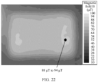
- FIG. 16 shows two magnetic field distribution diagrams: a magnetic field distribution diagram-1 and a magnetic field distribution diagram-2.
- the magnetic field distribution diagram-1 corresponds to the camera compact module 200 shown in FIG. 2 .
- the magnetic field distribution diagram-2 corresponds to the camera compact module 200 shown in FIG. 5 , and the magnetic field distribution diagram-2 may include the first magnetic isolation member 620 and the second magnetic isolation member 610 shown in FIG. 5 .
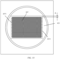
- An interfered plane in FIG. 16 may be a plane on which the image sensor 207 shown in FIG. 2 or FIG. 5 is located. It can be seen from FIG. 16 that, in the magnetic field distribution diagram-1, magnetic field intensity near the interfered plane is larger; and in the magnetic field distribution diagram-2, magnetic field intensity near the interfered plane is smaller.
- a magnetic field distribution diagram of a local observation region-1 shown in FIG. 17 may be obtained by locally observing a local observation region-1 in FIG. 16 .
- a magnetic field distribution diagram of a local observation region-2 shown in FIG. 17 may be obtained by locally observing a local observation region-2 in FIG. 16 .
- the magnetic field distribution diagram of the local observation region-1 may correspond to the camera compact module 200 shown in FIG. 2 .
- the magnetic field distribution diagram of the local observation region-2 may correspond to the camera compact module 200 shown in FIG. 5 .
- the first magnetic isolation member 620 and the second magnetic isolation member 610 shown in FIG. 5 are disposed in the magnetic field distribution diagram of the local observation region-1.
- both the first magnetic isolation member 620 and the second magnetic isolation member 610 are soft magnetic materials. Therefore, a magnetic field change occurs when the interference magnetic field passes through the second magnetic isolation member 610, and the magnetic field change occurs again when the interference magnetic field passes through the first magnetic isolation member 620. In addition, the phenomena such as the eddy current effect and the magnetic domain direction change may occur in both the first magnetic isolation member 620 and the second magnetic isolation member 610.
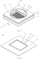
- FIG. 19 to FIG. 21 show another second magnetic isolation member 610 according to an embodiment of this application, and a position relationship among a first magnetic isolation member 620, the second magnetic isolation member 610, and a circuit board 203.
- FIG. 19 shows a schematic diagram of a three-dimensional structure of the first magnetic isolation member 620, the second magnetic isolation member 610, and the circuit board 203.
- FIG. 20 shows a schematic diagram of a structure of the first magnetic isolation member 620, the second magnetic isolation member 610, and the circuit board 203 at a first angle of view.
- the first angle of view may be an observation angle of view (that is, an observation angle of view parallel to an optical axis) shown by an arrow 1901 in FIG. 19 .
- FIG. 19 shows another second magnetic isolation member 610 according to an embodiment of this application, and a position relationship among a first magnetic isolation member 620, the second magnetic isolation member 610, and a circuit board 203.
- FIG. 19 shows a schematic diagram of a three-dimensional structure of the
- the second angle of view may be an observation angle of view (that is, an observation angle of view perpendicular to the optical axis) shown by an arrow 1902 in FIG. 19 .
- the second magnetic isolation member 610 shown in FIG. 19 may be used in the camera compact module 200 shown in FIG. 2 or FIG. 5 .
- the second magnetic isolation member 610 shown in FIG. 19 to FIG. 21 may include two second magnetic isolation edges 612, and each second magnetic isolation edge 612 surrounds the periphery of the second through hole 6111 and is disposed perpendicular to the second magnetic isolation board 611.
- Each second magnetic isolation edge 612 may be in a 1/Ni ring shape, where N 1 >2.
- N 1 may be, for example, 4, that is, each second magnetic isolation edge 612 is in a 1/4 ring shape.
- An inner wall (that is, a side wall closest to the optical axis of the lens array 2022 shown in FIG. 5 ) 6121 of each second magnetic isolation edge 612 may be in communication with the hole wall of the second through hole 6111.
- the two second magnetic isolation edges 612 may be symmetrically disposed relative to the central surface of the image sensor 207.
- a position of a second magnetic isolation edge 612 on the second magnetic isolation board 611 may be as close as possible to a pin 2071 of the image sensor 207 (for example, the second magnetic isolation edge 612 and the pin 2071 may be located on a same side of the camera compact module 200 shown in FIG. 5 ), to improve a magnetic isolation effect as much as possible.
- the second magnetic isolation edges 612 may also be asymmetrically disposed on the second magnetic isolation board 611.
- FIG. 22 shows a magnetic field distribution diagram corresponding to the embodiments shown in FIG. 19 to FIG. 21 .
- a plurality of embodiments according to this application in terms of magnetic flux are compared in Table 2. It can be seen that, compared with the embodiment shown in FIG. 2 , in the embodiments shown in FIG. 19 to FIG. 21 , a magnetic field interference degree to a magnetic sensitive component (including the image sensor 207, the power supply on the circuit board 203, and the like) may be reduced by about 44% to 46%. Compared with an embodiment in which only a single-layer soft magnetic material component is used, in the embodiments shown in FIG. 19 to FIG. 21 , the magnetic field interference degree to the magnetic sensitive component may be reduced by about 28% to 42%.
- the second angle of view may be an observation angle of view (that is, an observation angle of view perpendicular to the optical axis) shown by an arrow 2302 in FIG. 23 .
- the second magnetic isolation member 610 shown in FIG. 23 may be used in the camera compact module 200 shown in FIG. 2 or FIG. 5 .
- the second magnetic isolation member 610 shown in FIG. 23 to FIG. 25 may include more second magnetic isolation edges 612.
- the second magnetic isolation member 610 may include four second magnetic isolation edges 612, and each second magnetic isolation edge 612 may be in a 1/8 to 1/6 ring shape.
- the four second magnetic isolation edges 612 may be distributed at an equal spacing around the periphery of the second through hole 6111.
- the four second magnetic isolation edges 612 may be symmetrically disposed relative to the optical axis of the lens array 2022 shown in FIG. 5 .
- the plurality of second magnetic isolation edges 612 on the second magnetic isolation member 610 may also be asymmetrically distributed.
- the plurality of second magnetic isolation edges 612 on the second magnetic isolation member 610 may also be distributed at unequal spacings.
- FIG. 26 shows a magnetic field distribution diagram corresponding to the embodiments shown in FIG. 23 to FIG. 25 .
- a plurality of embodiments according to this application in terms of magnetic flux are compared in Table 4. It can be seen that, compared with the embodiment shown in FIG. 2 , in the embodiments shown in FIG. 23 to FIG. 25 , a magnetic field interference degree to a magnetic sensitive component (including the image sensor 207, the power supply on the circuit board 203, and the like) may be reduced by about 44% to 46%. Compared with an embodiment in which only a single-layer soft magnetic material component is used, in the embodiments shown in FIG. 23 to FIG. 25 , the magnetic field interference degree to the magnetic sensitive component may be reduced by about 28% to 42%.
- the embodiments shown in FIG. 23 to FIG. 25 may be conducive to reducing interference magnetic field to the image sensor 207.
- the second magnetic isolation edge is disposed in a comb shape on the second magnetic isolation board, thereby being conducive to reducing an overall weight of the second magnetic isolation member, and basically having no influence on a magnetic isolation effect of the second magnetic isolation member, and further being conducive to flexibly avoiding another component in the camera compact module.
- each second magnetic isolation edge 612 may be a small segment of a complete ring.
- each second magnetic isolation edge 612 may be in a 1/N ring shape, where N>n.
- the n second magnetic isolation edges 612 may be arranged to form a comb-shaped magnetic isolation edge assembly.
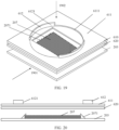
- FIG. 27 to FIG. 30 show another first magnetic isolation member 620 according to an embodiment of this application, and a position relationship among the first magnetic isolation member 620, a second magnetic isolation member 610, and a circuit board 203.
- FIG. 27 shows a schematic diagram of a three-dimensional structure of the first magnetic isolation member 620, the second magnetic isolation member 610, and the circuit board 203.
- FIG. 28 shows a schematic diagram of a structure of the first magnetic isolation member 620.
- FIG. 29 shows a schematic diagram of a structure of the first magnetic isolation member 620, the second magnetic isolation member 610, and the circuit board 203 at a first angle of view.
- the first angle of view may be an observation angle of view (that is, an observation angle of view parallel to an optical axis) shown by an arrow 2701 in FIG. 27 .
- FIG. 30 shows a schematic diagram of a structure of the first magnetic isolation member 620, the second magnetic isolation member 610, and the circuit board 203 at a second angle of view.
- the second angle of view may be an observation angle of view (that is, an observation angle of view perpendicular to the optical axis) shown by an arrow 2702 in FIG. 27 .
- the first magnetic isolation member 620 shown in FIG. 27 may be used in the camera compact module 200 shown in FIG. 2 or FIG. 5 .
- the first magnetic isolation member 620 shown in FIG. 27 to FIG. 30 may include a first magnetic isolation edge 622.
- the first magnetic isolation edge 622 may be disposed perpendicular to the first magnetic isolation board 621.
- the first magnetic isolation edge 622 may surround a periphery of the first through hole 6211, and is located on a side that is of the first magnetic isolation board 621 and that is away from the image sensor 207.
- the first magnetic isolation edge 622 may be in a block shape.
- a height h 4 of the first magnetic isolation edge 622 may be greater than or equal to 0.01 mm.
- the height h 4 of the first magnetic isolation edge 622 may be 0.1 mm.
- the height h 4 of the first magnetic isolation edge 622 may be less than a distance between the first magnetic isolation board 621 and the lens array 2022.
- an inner wall that is, a side wall of the first magnetic isolation edge 622 closest to the optical axis of the lens array 2022 shown in FIG. 5
- 6221 of the first magnetic isolation edge 622 may be in communication with the hole wall of the first through hole 6211.
- a step surface is disposed between the inner wall 6221 of the first magnetic isolation edge 622 and the hole wall of the first through hole 6211, and the step surface may be disposed in parallel with the first magnetic isolation board 621.
- the first magnetic isolation member 620 may include a plurality of first magnetic isolation edges 622, and each first magnetic isolation edge 622 may be perpendicularly disposed on the first magnetic isolation board 621. Each first magnetic isolation edge 622 may surround a periphery of the first through hole 6211. In an example, the inner wall 6221 of each first magnetic isolation edge 622 may be in communication with the hole wall of the first through hole 6211. In an example, when the first through hole 6211 is a square hole, any first magnetic isolation edge 622 may be in a long strip shape or a corner shape.
- the plurality of first magnetic isolation edges 622 may be symmetrically distributed or distributed at an equal spacing. In an example, when there are a larger quantity of first magnetic isolation edges 622, the n first magnetic isolation edges 622 may be arranged to form a comb-shaped magnetic isolation edge assembly.
- FIG. 32 shows a position relationship among a first magnetic isolation member 620, a second magnetic isolation member 610, and a circuit board 203 according to an embodiment of this application.
- first magnetic isolation member 620 refer to the embodiment shown in FIG. 27 . Details are not described herein again.
- FIG. 33 shows a position relationship among a first magnetic isolation member 620, a second magnetic isolation member 610, and a circuit board 203 according to an embodiment of this application.
- first magnetic isolation member 620 refer to the embodiment shown in FIG. 27 . Details are not described herein again.
Landscapes
- Engineering & Computer Science (AREA)
- Signal Processing (AREA)
- Physics & Mathematics (AREA)
- Multimedia (AREA)
- General Physics & Mathematics (AREA)
- Electromagnetism (AREA)
- Optics & Photonics (AREA)
- Studio Devices (AREA)
- Camera Bodies And Camera Details Or Accessories (AREA)
Applications Claiming Priority (2)
| Application Number | Priority Date | Filing Date | Title |
|---|---|---|---|
| CN202011365693.6A CN114584636B (zh) | 2020-11-28 | 2020-11-28 | 形状记忆合金马达、马达模组、摄像头模组、电子设备 |
| PCT/CN2021/133362 WO2022111614A1 (zh) | 2020-11-28 | 2021-11-26 | 形状记忆合金马达、马达模组、摄像头模组、电子设备 |
Publications (3)
| Publication Number | Publication Date |
|---|---|
| EP4239983A1 true EP4239983A1 (de) | 2023-09-06 |
| EP4239983A4 EP4239983A4 (de) | 2024-06-26 |
| EP4239983B1 EP4239983B1 (de) | 2026-01-28 |
Family
ID=81753770
Family Applications (1)
| Application Number | Title | Priority Date | Filing Date |
|---|---|---|---|
| EP21897114.1A Active EP4239983B1 (de) | 2020-11-28 | 2021-11-26 | Motor aus einer formgedächtnislegierung, motormodul, kameramodul, elektronische vorrichtung |
Country Status (4)
| Country | Link |
|---|---|
| US (1) | US12501131B2 (de) |
| EP (1) | EP4239983B1 (de) |
| CN (1) | CN114584636B (de) |
| WO (1) | WO2022111614A1 (de) |
Families Citing this family (1)
| Publication number | Priority date | Publication date | Assignee | Title |
|---|---|---|---|---|
| US12301744B2 (en) * | 2022-01-10 | 2025-05-13 | Apple Inc. | Handheld electronic device |
Family Cites Families (8)
| Publication number | Priority date | Publication date | Assignee | Title |
|---|---|---|---|---|
| US10866382B2 (en) * | 2016-07-22 | 2020-12-15 | Cambridge Mechatronics Limited | PWM screening in a camera |
| CN208207475U (zh) * | 2018-03-09 | 2018-12-07 | 欧菲影像技术(广州)有限公司 | 移动终端的摄像模组及其摄像头 |
| GB201816864D0 (en) * | 2018-10-16 | 2018-11-28 | Cambridge Mechatronics Ltd | Electromagnetic screening of an image sensor from an actuator in a camera |
| CN109151288B (zh) * | 2018-10-30 | 2021-01-08 | 维沃移动通信(杭州)有限公司 | 补光模组及终端设备 |
| CN110572749B (zh) * | 2018-11-16 | 2021-03-23 | 华为技术有限公司 | 一种移动终端 |
| CN109302556B (zh) * | 2018-11-30 | 2024-08-13 | 上海信迈电子科技有限公司 | 防抖结构、防抖系统及具有其的摄像装置 |
| JP2020086465A (ja) * | 2018-11-30 | 2020-06-04 | 新思考電機有限公司 | 駆動装置、カメラ装置及び電子機器 |
| CN111385446B (zh) * | 2018-12-27 | 2025-11-21 | 华为技术有限公司 | 摄像头组件及用户设备 |
-
2020
- 2020-11-28 CN CN202011365693.6A patent/CN114584636B/zh active Active
-
2021
- 2021-11-26 EP EP21897114.1A patent/EP4239983B1/de active Active
- 2021-11-26 WO PCT/CN2021/133362 patent/WO2022111614A1/zh not_active Ceased
- 2021-11-26 US US18/254,681 patent/US12501131B2/en active Active
Also Published As
| Publication number | Publication date |
|---|---|
| EP4239983A4 (de) | 2024-06-26 |
| CN114584636A (zh) | 2022-06-03 |
| WO2022111614A1 (zh) | 2022-06-02 |
| EP4239983B1 (de) | 2026-01-28 |
| US20230421873A1 (en) | 2023-12-28 |
| US12501131B2 (en) | 2025-12-16 |
| CN114584636B (zh) | 2023-11-03 |
Similar Documents
| Publication | Publication Date | Title |
|---|---|---|
| US20240280880A1 (en) | Aperture Assembly, Camera Module, and Electronic Device | |
| KR102782703B1 (ko) | 보이스 코일 모터, 카메라 모듈, 및 전자 디바이스 | |
| CN209657058U (zh) | 光学摄像系统 | |
| KR102823514B1 (ko) | 카메라 모듈 및 이를 포함하는 광학 기기 | |
| EP3573324B1 (de) | Kameraanordnung und elektronische vorrichtung | |
| KR20220035970A (ko) | 광학 이미지 안정화 장치 및 제어 방법 | |
| KR20180111263A (ko) | 카메라 모듈 | |
| JP7616753B2 (ja) | カメラモジュール及び電子装置 | |
| CN110187463A (zh) | 自动聚焦驱动组件、镜头及电子设备 | |
| JP2025541980A (ja) | ボイスコイルモータ、光学画像安定化アセンブリ、コンパクトカメラモジュールおよび電子デバイス | |
| US11977320B2 (en) | Camera module and electronic device | |
| KR20220070277A (ko) | 카메라 모듈 및 단말 디바이스 | |
| CN108769515B (zh) | 电子设备 | |
| US12501131B2 (en) | Shape memory alloy motor, motor module, camera compact module, and electronic device | |
| GB2611381A (en) | Camera module, information processing method, and electronic device | |
| TW202328792A (zh) | 相機模組與電子裝置 | |
| EP4472189A1 (de) | Elektronische vorrichtung und kameramodul und steuerungsverfahren dafür | |
| EP3588159B1 (de) | Mobiles endgerät mit periskopischem linsenmodul | |
| EP4239984A1 (de) | Motor aus einer formgedächtnislegierung, motormodul, kameramodul und elektronische vorrichtung | |
| US20240069356A1 (en) | Camera module | |
| JP2011085675A (ja) | 光学素子駆動装置及び撮像装置 | |
| US20230209159A1 (en) | Camera module | |
| KR102187735B1 (ko) | 카메라 모듈 | |
| US20240419055A1 (en) | Iris module and camera module including the same | |
| CN115002318B (zh) | 摄像装置和电子设备 |
Legal Events
| Date | Code | Title | Description |
|---|---|---|---|
| STAA | Information on the status of an ep patent application or granted ep patent |
Free format text: STATUS: THE INTERNATIONAL PUBLICATION HAS BEEN MADE |
|
| PUAI | Public reference made under article 153(3) epc to a published international application that has entered the european phase |
Free format text: ORIGINAL CODE: 0009012 |
|
| STAA | Information on the status of an ep patent application or granted ep patent |
Free format text: STATUS: REQUEST FOR EXAMINATION WAS MADE |
|
| 17P | Request for examination filed |
Effective date: 20230504 |
|
| AK | Designated contracting states |
Kind code of ref document: A1 Designated state(s): AL AT BE BG CH CY CZ DE DK EE ES FI FR GB GR HR HU IE IS IT LI LT LU LV MC MK MT NL NO PL PT RO RS SE SI SK SM TR |
|
| DAV | Request for validation of the european patent (deleted) | ||
| DAX | Request for extension of the european patent (deleted) | ||
| REG | Reference to a national code |
Ref country code: DE Ref legal event code: R079 Ipc: H04N0023520000 Ref country code: DE Ref legal event code: R079 Ref document number: 602021047326 Country of ref document: DE Free format text: PREVIOUS MAIN CLASS: H04M0001020000 Ipc: H04N0023520000 |
|
| A4 | Supplementary search report drawn up and despatched |
Effective date: 20240527 |
|
| RIC1 | Information provided on ipc code assigned before grant |
Ipc: H04N 23/55 20230101ALI20240521BHEP Ipc: H04N 23/54 20230101ALI20240521BHEP Ipc: H04M 1/02 20060101ALI20240521BHEP Ipc: H04N 23/52 20230101AFI20240521BHEP |
|
| GRAP | Despatch of communication of intention to grant a patent |
Free format text: ORIGINAL CODE: EPIDOSNIGR1 |
|
| STAA | Information on the status of an ep patent application or granted ep patent |
Free format text: STATUS: GRANT OF PATENT IS INTENDED |
|
| RIC1 | Information provided on ipc code assigned before grant |
Ipc: H04N 23/52 20230101AFI20250811BHEP Ipc: H04N 23/54 20230101ALI20250811BHEP Ipc: H04N 23/55 20230101ALI20250811BHEP Ipc: G02B 7/08 20210101ALI20250811BHEP Ipc: G02B 27/64 20060101ALI20250811BHEP Ipc: G03B 30/00 20210101ALI20250811BHEP Ipc: H04N 25/617 20230101ALI20250811BHEP Ipc: H04M 1/02 20060101ALI20250811BHEP |
|
| INTG | Intention to grant announced |
Effective date: 20250908 |
|
| GRAS | Grant fee paid |
Free format text: ORIGINAL CODE: EPIDOSNIGR3 |
|
| GRAA | (expected) grant |
Free format text: ORIGINAL CODE: 0009210 |
|
| STAA | Information on the status of an ep patent application or granted ep patent |
Free format text: STATUS: THE PATENT HAS BEEN GRANTED |
|
| AK | Designated contracting states |
Kind code of ref document: B1 Designated state(s): AL AT BE BG CH CY CZ DE DK EE ES FI FR GB GR HR HU IE IS IT LI LT LU LV MC MK MT NL NO PL PT RO RS SE SI SK SM TR |
|
| REG | Reference to a national code |
Ref country code: CH Ref legal event code: F10 Free format text: ST27 STATUS EVENT CODE: U-0-0-F10-F00 (AS PROVIDED BY THE NATIONAL OFFICE) Effective date: 20260128 Ref country code: GB Ref legal event code: FG4D |