EP4238006B1 - Verteilte synaptische mehrkomponenten-rechenstruktur - Google Patents
Verteilte synaptische mehrkomponenten-rechenstruktur Download PDFInfo
- Publication number
- EP4238006B1 EP4238006B1 EP21805450.0A EP21805450A EP4238006B1 EP 4238006 B1 EP4238006 B1 EP 4238006B1 EP 21805450 A EP21805450 A EP 21805450A EP 4238006 B1 EP4238006 B1 EP 4238006B1
- Authority
- EP
- European Patent Office
- Prior art keywords
- synaptic
- presynaptic
- weight application
- application elements
- output
- Prior art date
- Legal status (The legal status is an assumption and is not a legal conclusion. Google has not performed a legal analysis and makes no representation as to the accuracy of the status listed.)
- Active
Links
Images


Classifications
-
- G—PHYSICS
- G06—COMPUTING OR CALCULATING; COUNTING
- G06N—COMPUTING ARRANGEMENTS BASED ON SPECIFIC COMPUTATIONAL MODELS
- G06N3/00—Computing arrangements based on biological models
- G06N3/02—Neural networks
- G06N3/04—Architecture, e.g. interconnection topology
- G06N3/049—Temporal neural networks, e.g. delay elements, oscillating neurons or pulsed inputs
-
- G—PHYSICS
- G06—COMPUTING OR CALCULATING; COUNTING
- G06N—COMPUTING ARRANGEMENTS BASED ON SPECIFIC COMPUTATIONAL MODELS
- G06N3/00—Computing arrangements based on biological models
- G06N3/02—Neural networks
- G06N3/06—Physical realisation, i.e. hardware implementation of neural networks, neurons or parts of neurons
- G06N3/063—Physical realisation, i.e. hardware implementation of neural networks, neurons or parts of neurons using electronic means
- G06N3/065—Analogue means
Definitions
- the present invention relates to automatic signal recognition techniques, and more particularly, to a system and method for distributed multi-component synaptic computational structures that allows area-optimized and energy-efficient processing mechanisms in networks.
- the computational structures are spiking neural networks.
- synaptic dynamics are replicated by the presynaptic integrator 213 and the weight application elements 211.
- the presynaptic integrator 213, performs the function of presynaptic pulse (spike) integration, such that a presynaptic (fast) pulse signal 204 is translated into a (long-lasting) synaptic input signal 214.
- the synaptic input signal 214 may be an exponentially decreasing spike, similar to a signal emitted by an AMPA-receptor.
- the synaptic input signal 214 may be a synaptic input current.
- the synaptic input signal 214 may be a synaptic input voltage.
- the presynaptic integrator 213 is configurable by a control signal 203, preferably wherein the control signal 203 controls the temporal shape of the synaptic input signals 214 generated by the presynaptic integrator 213.
- the spiking neural network further comprises a row spike decoder 202, configured to decode and allocate the presynaptic pulse signals 204 to the corresponding presynaptic integrators 213, based on a presynaptic input spike 201.
- a row spike decoder 202 configured to decode and allocate the presynaptic pulse signals 204 to the corresponding presynaptic integrators 213, based on a presynaptic input spike 201.
- Which presynaptic pulse signals to send to which presynaptic integrator 213 depends of the configuration of the spiking neural network. Decoding the presynaptic input spike 201 encompasses.
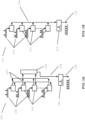
- FIG. 3 shows a another example of a part of a spiking neural network 300 according to another exemplary embodiment, which may form a sub-network (or ensemble) within a larger neural network comprising a plurality of sub-networks, and may be implemented as a neuro-synaptic core.
- the output neurons 322 are connected to weight application elements 311, which are connected to presynaptic integrators 313.
- Exemplary embodiments include at least one presynaptic integrator 313, a plurality 310 of weight application elements 311 and a plurality 320 of output neurons 322.
- the spiking neural network 300 comprises several layers, such that the spatio-temporal spike train output signal 326 generated by the output neurons 322 may form the presynaptic signal 204 received by a presynaptic integrator 213 in a next layer, and such that the presynaptic pulse signal 307 received by a presynaptic integrator 313 may be generated by an input neuron, i.e. an output neuron 322 from a previous layer.
- an input neuron i.e. an output neuron 322 from a previous layer.
- presynaptic integrators 313 and weight application elements 311 are shown, and only some have a reference numeral attached to them.
- a sub-network, or ensemble of neurons that form a co-operative group can for example form a classifier, an ensemble of classifiers, groups of neurons that handle data conversion, feature encoding or solely the classification, et cetera.
- a large network of ensembles is partitioned and mapped onto an array of cores, each of which contains a programmable network of spiking neurons.
- Each core consequently implements a single ensemble, multiple small ensembles (in relation to the number of neurons and synapses in the core), or in the case of large ensembles, only a part of a single ensemble, with other parts implemented on other cores of the array.
- the modalities of how ensembles are partitioned and mapped to cores is determined by a mapping methodology.
- the mapping methodology can comprise a constraint-driven partitioning.
- the constraint can be a performance metric linked to the function of each respective sub-network.
- the performance metric could be dependent on power-area limitations, memory structures, memory access, time constants, biasing, technology restrictions, resilience, a level of accepted mismatch, and network or physical artifacts.
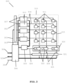
- the neurosynaptic core control element 304 is configured to receive a spike input 306, possibly from a previous layer of input neurons, to send the presynaptic input spike 301 to the row spike decoder 302, and to send the control signals 303 to the presynaptic integrators 303. Further, the neurosynaptic core control element 304 is configured to receive and subsequently transmit a neuron spike output signal 325 from the neuron decoder element 321. Additionally, the neurosynaptic core control element 304 is configured to control both the neuron control element 323 and the neuron decoder element 321. Finally, the neurosynaptic core control element is configurable by a configuration signal 305.
- the neuron control element 323 is configured to control the plurality 320 of output neurons 322 through a neuron control signal 324.
- the neuron decoder element 321 is configured to generate a neuron spike output signal 325 based on at least one spatio-temporal spike train output signal 326, generated by an output neuron 322 based on a synaptic output current 315.
- the neuro-synaptic core disclosed in the present invention can thus be organized as repeating arrays of synaptic circuits and neuron units, where each unit can form a cell assembly.
- the system can incorporate the presence of electronic synapses at the junctions of the array.
- the periphery of the array can include rows of the synaptic circuits which mimic the action of the soma and axon hillock of biological neurons.
- each neuro-synaptic core in the array can have a local router, which communicates to the routers of other cores within a dedicated real-time reconfigurable network-on-chip.
- a classifier can e.g. be assumed to have a set of output neurons (one for each class) each of which fires an event (spike) according to its firing probability distribution.
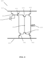
- FIG. 4A shows a presynaptic integration circuit 400 according to an exemplary embodiment not falling under the scope of the appended claims of a presynaptic integrator 213, 313, comprising a positive voltage supply 420 (also called a drain with voltage V DD ), a negative voltage supply 440 (also called a source with voltage V SS ), a capacitor 404, several field effect transistors (FETs), in particular an input FET 401, a leakage FET 403, an output FET 405, and a current mirror 406.
- the presynaptic integrator 213, 313 operates in the sub-threshold region and offers a low area and linear filtering properties.
- the presynaptic integrator 213, 313 translates fast presynaptic pulse signals 204, 307 into (long-lasting) synaptic input signals 214, 314.
- the synaptic input signals may, for example, be shaped like an exponentially decreasing spike (while preserving AMPA-like receptor temporal dynamics).
- the presynaptic integrator 213, 313 offers the possibility of multiplexing time spikes originating from different neurons, and provides tunable gain independent from the (tunable) time constant.
- the current mirror 406 may be a cascode current mirror such that the synaptic input signal 214, 314 comprises two voltage signals, for reduced variation and increased accuracy of current replication. Namely, the cascode implementation improves the output drive strength, by improving impedance.
- FIG. 4B shows a presynaptic integration circuit 410 according to another exemplary embodiment not falling under the scope of the appended claims of a presynaptic integrator 213, 313, comprising a positive voltage supply 430, a negative voltage supply 450, a capacitor 414, several field effect transistors (FETs), in particular input FETs 411, a control FET 412 a leakage FET 413, an output FET 415, a mirror FET 417 and a cascode current mirror 416.
- FETs field effect transistors
- This embodiment further includes an output control element, comprising an output control FET 419, a current control FET 418 and an inverter 423.
- the presynaptic pulse signal 204, 307 is the gate-source voltage over the input FETs 411. If the gate-source voltage over input FETs 411 goes high when an input pulse is applied, a current starts to flow, through control FET 412, charging capacitor 414 to the diode voltage of mirror FET 417. It is important to note that gate-source voltage pulse on input FETS 411 needs to be long enough in order for the amount of charge accumulated by the capacitor 414 to reach a constant value.
- the control FET 412 is configured to control the temporal dynamic of the synaptic input signal 214, 314 based on the control signal 203, 303.
- the control signal 203, 303 is the gate-source voltage over the control FET 402. When the gate-source voltage is positive, the control FET 412 turns on, enabling a drain-source current to flow.
- the control signal 203, 303 is configured to regulate the accumulation of charge by the capacitor, such that the amount of charge accumulated by the capacitor is independent of a duration of a spike in the spatio-temporal spike train and the capacitance value of the capacitor, and to regulate the temporal shape and maximum amplitude of the synaptic input signal by controlling the maximum charge on the capacitor.
- control FET 412 is a constant current source.
- the capacitor 414 is connected to input FETs 411 and control FET 412 such that when both input FETs 411 and control FET 412 are turned on, a closed circuit is formed, connecting the positive voltage supply 430 to the negative voltage supply 450 through the capacitor 414, such that the capacitor 414 accumulates charge until the connection ends.
- the output FET 415 turns on, as its gate-source voltage is equal to the charge accumulated by the capacitor 414.
- the presynaptic pulse signal 204, 307 goes low, the output is enabled; as leakage FET 413 discharges capacitor 414 over time, the drain-source current over output FET 415 will decrease accordingly
- both the output FET 415 and the output control FET 419 are turned on, a drain-source current flow is enabled from the positive voltage supply 430 to the negative voltage supply 450, through the output FET 415, the output control FET 419 and the cascode current mirror 416.
- the output FET 415 may be configured to operate in its sub-threshold region, such that if the charge on capacitor 414 is decreasing linearly, the drain-source current over the output FET 415 decreases exponentially.
- the output stage can employ a cascode current mirror 416 for reduced variation and increased accuracy of the current replication. If a current flows through the cascode current mirror 416, two voltage signals are generated proportional to the strength of said current.
- the synaptic input signal 214, 314 generated by the presynaptic integrator 213, 313 thus comprises two voltage signals.
- the current flowing through cascode current mirror 416 is replicated as two voltage signals.
- the cascode current mirror 416 may be a regular current mirror producing one voltage signal instead as was seen in the embodiment of FIG. 4A , not falling under the scope of the appended claims.
- the output control element comprising the inverter 423, the output control FET 419 and current control FET 418, is configured to regulate the flow of an output current.
- Arrow 421 denotes the direction of the output current over the drain-source of output FET 415. However, this current only flows if both the output FET 415 and output control FET 419 are turned on.
- the inverter 423 is connected to an input FET 411, such that a positive voltage is generated at its output if the presynaptic input signal 204, 307 is negative, and a negative voltage is generated at the output of inverter 423 if the presynaptic input signal 204, 307 is positive.
- the output control FET 419 only turns on if the presynaptic input signal is negative, that is, when the presynaptic input signal is not spiking. Output current flow over FETs 415 and 419 is thus only possible after a spike in the spatio-temporal spike train has ended. Additionally, the current control FET 418 is only turned on when the presynaptic pulse signal 204, 307 is spiking. As a consequence, discharging of the capacitor 414 by the drain-source current over either of FETs 418 and 411 is not possible after a spike has ended, making sure that the discharging of capacitor 414 is controlled by the leakage FET 413.
- the leakage FET 413 is configured to discharge the capacitor 414 through its drain-source current (current direction indicated by arrow 422), if it is turned on.
- capacitor 414 discharges with a constant current through leakage FET 413.
- the leakage FET 413 is controlled by a time constant, the time constant determining the gate-source voltage of the leakage FET 413.
- the time constant may be chosen such that AMPA, NDMA, GABA A or GABA B temporal dynamics are realised.
- the mirror FET 417 is coupled to the output FET 415, such that the mirror FET 417 and output FET 415 together form a current mirror, ensuring that the drain-source current over the output FET 415 is identical to the drain-source current over the mirror FET 417. Therefore the voltage induced by the capacitor within the pre-integration circuit does not matter anymore for the functioning of the pre-integration circuit.
- the weight application (multiplication) circuit of Fig. 2 and Fig. 3 is fully distributed and performs the typical synaptic function, connecting the input and output neurons and applying a stored weight.
- the linearity of the multiplier should be preserved in order to not-degrade learning.
- the digitally stored weights are transformed to an analog domain through a current-steering D/A converter based on an R-2R architecture, which is shown in Figs. 5A and 5B .
- the weight application element may apply a factor ranging from zero to one on its input current, attenuating it, and sending the selected portion of the input current to its output.
- FIG. 5A shows a weight application circuit 500 according to an exemplary embodiment not falling under the scope of the appended claims of a weight application element 211, 311.
- the weight application circuit 500 comprises a positive voltage supply 520, a negative voltage supply 540, a first synaptic input receiver 507, a second synaptic input receiver 508, an output terminal 509, and a ladder of output selection elements 550, each comprising dual resistance FETs 503, a single resistance FET 504, a positive output FET 501 and a negative output FET 502.
- FET 505 and FET 506 can also be connected to the positive voltage supply 520.
- the synaptic input receivers 507 and 508 are configured to receive a synaptic input signal 214, 314 in the form of a gate-source voltage. With reference to Fig. 4A not falling under the scope of the appended claims, the synaptic input signal 214, 314 may be provided by output current mirror 406.
- the gate-source voltages over synaptic input receivers 507, 508 enable current flow through the rest of the weight application circuit 500, particularly along the ladder of output selection elements 550 to the output terminal 509.
- the output selection elements 550 are connected sequentially, such that the current flowing through synaptic input receiver 507 is distributed among the output selection elements 550.
- Each of the output selection elements 550 comprises a single resistance transistor 504 and dual resistance transistors 503, which are positioned such that the current from the synaptic input receiver 507 is divided by two for each output selection element 550 it passes.
- the first output selection element 550 receives half of the synaptic input current
- the second output selection element 550 receives a fourth
- the third output selection element 550 receives an eighth, and so on.
- the more output selection elements 550 are included, the more accuracy is attainable in weight application.
- Each of the output selection elements 550 comprises a positive output FET 501 and a negative output FET 502.
- the gate-source voltages over these FETs are determined by the digitally stored weight values, stored in the weight storage elements 212.
- the weight values are stored as bits, with the amount of bits equal to the amount of output control elements 550.
- Each bit of the stored weight value determines the setting of an output control element, such that either the positive output FET 501 or the negative output FET 502 is turned on. If the positive output FET 501 is turned on, the portion of the synaptic input current that is allocated to the corresponding output selection element is connected to the output terminal 509. If the negative output FET 502 is turned on, the selected portion of the synaptic input current does not contribute to the synaptic output current. As such, a weight application based on a stored binary weight value is realized.
- FIG. 5B shows a weight application circuit 500 according to another exemplary embodiment not falling under the scope of the appended claims of a weight application element 211, 311.
- the synaptic input receivers 507, 508 each comprise two field effect transistors, configured to receive the synaptic input signal 214, 314 in the form of two gate-source voltages.
- the synaptic input signal 214, 314 may be provided by output cascode current mirror 416.
- FIG. 6 shows a polarity selection circuit 600 according to an exemplary embodiment not falling under the scope of the appended claims, comprising a polarity selection
- the polarity of the output of a weight application element 211, 311 may be configurated to generate inhibitory spikes, corresponding to the behaviour of GABA receptors.
- the polarity selection circuit 600 employs a sourcing current mirror 632 sourcing current and a sinking current mirror 642 sinking current.
- the polarity selection circuit further comprises a positive voltage supply 610, a negative voltage supply 620, a polarity output element 603, a first passage FET 631, a second passage FET 641, a sourcing selection FET 630, a sinking selection FET 640, and a polarity input element 601 configured to receive the synaptic output current 215, 315.
- the direction of the synaptic output current 215, 315 is indicated by arrow 604.
- the sourcing current mirror or sinking current mirror is enabled, corresponding to an excitatory or inhibitory synapse, respectively.
- the polarity input element 601 is configured to receive the synaptic output current as a drain-source current, and to translate this current to a gate-source voltage. This gate-source voltage is applied to the gate terminal of either the sourcing current mirror 632 or the sourcing current mirror 642.
- the passage FETs 631 and 632 are configured to pass the signal received by the polarity input element 601 to the sinking current mirror, if applicable. If a voltage is applied to the gate of the first passage FET 631, a drain-source current starts to flow. This drain source current determines the drain-source current flowing through the second passage FET 641, which determines the gate-source voltage of the second passage FET 641. This gate-source voltage applied to passage FET 641 may then be applied to the sinking current mirror 642, if the sinking selection FET 640 is turned on. The gate-source voltage over the second passage FET 641 will be identical to the gate-source voltage generated by polarity input element 601.
- polarity selection terminal 602 If either a high or a low voltage is applied to polarity selection terminal 602, either the sourcing selection FET 630 is turned on, or the sinking selection FET 640 is turned on.
- sinking selection FET 640 If the sinking selection FET 640 is turned on, a drain-source current over the sinking selection FET 640 is enabled. As a consequence, the gate-source voltage over the polarity input element 601 is also applied to sinking current mirror 642, turning the sinking current mirror 642 on. If the sinking current mirror 642 is turned on, a current starts to flow from the polarity output element 603 to the negative voltage supply 620. Thus, a current equal to the inverted synaptic input current received by the polarity input element 601 flows through the polarity output element 603.
- the spiking neural network can be implemented, without loss of generality, as a conductance-based integrate and fire model, which is one possible implementation of a generalized integrate and fire model.
- a spiking neural network according to the present invention can display a wide range of pattern activity, for example full synchrony, cluster or asynchronous states, depending on the excitatory/inhibitory network interaction conditions, heterogeneities in the input patterns, and the spatio-temporal dynamics implemented in the presynaptic integrators.
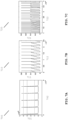
- FIG. 7A shows a graph 700 plotting excitatory synaptic output current (or excitatory postsynaptic current, i.e. synaptic EPSC current) 701 in Amperes as a function of time 702 in seconds, wherein the excitatory synaptic output current 701 is one exemplary embodiment of a synaptic output current 215, 315.
- excitatory synaptic output current or excitatory postsynaptic current, i.e. synaptic EPSC current
- FIGS 7B and 7C show graphs 710, 720 plotting voltage of a spatio-temporal spike train 711, 721 in Volts as a function of time 712, 722 in seconds wherein the spatio-temporal spike train is an exemplary embodiment of a spatio-temporal spike train 204, 307.
- FIG. 7B shows that accumulating charge on the membrane of a neuron (node) leads to spike generation.
- Fig. 7C non-linear spiking behaviour and frequency adaptability is shown.
- the current invention is implemented on an integrated circuit, and can be in particular on a microcontroller integrated circuit.
- the cores in the core array can form a network-on-chip on the microcontroller integrated circuit.
- the network-on-chip improves the scalability and the power efficiency of the microcontroller integrated circuit.
- the network-on-chip can be real-time reconfigurable, or statically defined during the production phase. When the network-on-chip is real-time reconfigurable, the settings of the cores in the core array and their interconnect structure settings can be altered. This alteration can be done based for example on changing input or output of the microcontroller integrated circuit, different demands on accuracy or stability of the classification, the evolution of the network based on its learning rules and a change in communication protocols.
- the current invention provides implementation of distributed multi-component hardware structure that enables optimal area and power design of synaptic processing functions. It can realize increase in synaptic structure dimensionality by allowing per-component optimization of individual signal processing characteristics and functions within the spiking neural network.
- the current invention provides implementation of an area- and power-efficient presynaptic adaptation mechanism that is robust against array inhomogeneities, where only a single spike integrator (instead of n) for every input neuron is required.
- the current invention provides implementation of a mechanism to select between excitatory and inhibitory output in a synaptic element. It provides implementation of synaptic elements capable of generating complex dynamics that can be extended towards particular functionality, such as the change in temporal characteristic, to perform time-dependent computations.
Landscapes
- Engineering & Computer Science (AREA)
- Physics & Mathematics (AREA)
- Theoretical Computer Science (AREA)
- Health & Medical Sciences (AREA)
- Life Sciences & Earth Sciences (AREA)
- Biomedical Technology (AREA)
- Biophysics (AREA)
- Computing Systems (AREA)
- Software Systems (AREA)
- Evolutionary Computation (AREA)
- General Health & Medical Sciences (AREA)
- Molecular Biology (AREA)
- Computational Linguistics (AREA)
- General Engineering & Computer Science (AREA)
- General Physics & Mathematics (AREA)
- Mathematical Physics (AREA)
- Data Mining & Analysis (AREA)
- Artificial Intelligence (AREA)
- Neurology (AREA)
- Image Analysis (AREA)
- Multi Processors (AREA)
- Management, Administration, Business Operations System, And Electronic Commerce (AREA)
- Arrangements For Transmission Of Measured Signals (AREA)
- Networks Using Active Elements (AREA)
- Analogue/Digital Conversion (AREA)
Claims (15)
- Integrierte Schaltung, die ein gepulstes neuronales Netz (100) implementiert, umfassend eine Vielzahl von präsynaptischen Integratoren (209), eine Vielzahl von Gewichtungsanwendungselementen (210) und eine Vielzahl von Ausgangsneuronen (220);wobei jeder der Vielzahl von präsynaptischen Integratoren (213) geeignet ist, um ein präsynaptisches Impulssignal (204) zu empfangen, das eine Akkumulation von Ladung innerhalb des präsynaptischen Integrators in einem Kondensator anregt, der konfiguriert ist, um die Ladung als Reaktion auf das präsynaptische Impulssignal zu akkumulieren und ein synaptisches Eingangssignal (214) basierend auf der akkumulierten Ladung zu erzeugen, derart, dass das synaptische Eingangssignal eine zuvor bestimmte zeitliche Dynamik aufweist;wobei eine erste Gruppe von Gewichtungsanwendungselementen (211) der Vielzahl von Gewichtungsanwendungselementen (210) verbunden ist, um das synaptische Eingangssignal (214) von einem ersten der Vielzahl von präsynaptischen Integratoren (213) zu empfangen;wobei jedes Gewichtungsanwendungselement (211) der ersten Gruppe von Gewichtungsanwendungselementen geeignet ist, um einen Gewichtungswert auf das synaptische Eingangssignal (214) anzuwenden, um einen synaptischen Ausgangsstrom (215) zu erzeugen, wobei die Stärke des synaptischen Ausgangsstroms von dem angewendeten Gewichtungswert abhängig ist; undwobei jedes der Vielzahl von Ausgangsneuronen (222) verbunden ist, um einen synaptischen Ausgangsstrom (214) von einer zweiten Gruppe von Gewichtungsanwendungselementen der Vielzahl von Gewichtungsanwendungselementen zu empfangen und ein räumlich-zeitliches Spike-Train-Ausgangssignal (223) basierend auf dem empfangenen einen oder den mehreren synaptischen Ausgangsströmen zu erzeugen, derart, dass jedes der Vielzahl von Ausgangsneuronen (222) seinen eigenen Satz von Gewichtungsanwendungselementen aufweist, von dem es synaptische Ausgangsströme empfängt, wobei dieser Satz von Gewichtungsanwendungselementen eine zweite Gruppe von Gewichtungsanwendungselementen ausbildet, und jedes dieser Gewichtungsanwendungselemente dieses eigenen Satzes von Gewichtungsanwendungselementen das synaptische Eingangssignal (214) von einem anderen der Vielzahl von präsynaptischen Integratoren empfängt und somit jedes dieser Gewichtungsanwendungselemente dieses eigenen Satzes von Gewichtungsanwendungselementen jeweils in einer anderen ersten Gruppe von Gewichtungsanwendungselementen enthalten ist.
- Integrierte Schaltung nach Anspruch 1, wobei jedes der Gewichtungsanwendungselemente eine Gewichtungsanwendungsschaltung umfasst, umfassend:einen synaptischen Eingangsempfänger, der konfiguriert ist, um das synaptische Eingangssignal von dem präsynaptischen Integrator zu empfangen und basierend auf dem synaptischen Eingangssignal einen synaptischen Eingangsstrom zu erzeugen;ein Gewichtungsspeicherelement, das konfiguriert ist, um den Gewichtungswert zu speichern;ein Modifikationselement, das konfiguriert ist, um den Gewichtungswert, der in dem Gewichtungsspeicherelement gespeichert ist, auf den synaptischen Eingangsstrom anzuwenden, um den synaptischen Ausgangsstrom zu erzeugen;wobei der Gewichtungswert vorzugsweise in digitaler Form gespeichert und durch einen stromlenkenden Digital-Analog-Wandler in einen analogen Bereich transformiert wird,wobei der stromlenkende Digital-Analog-Wandler vorzugsweise auf einer R-2R-Architektur basiert, undwobei der stromlenkende Digital-Analog-Wandler vorzugsweise einen zuvor bestimmten Faktor anwendet, um den synaptischen Eingangsstrom zu dämpfen, und den synaptischen Ausgangsstrom basierend auf dem gedämpften synaptischen Eingangsstrom erzeugt.
- Integrierte Schaltung nach Anspruch 2, wobei der Gewichtungswert, der in dem Gewichtungsspeicherelement gespeichert ist, anpassbar ist, vorzugsweise wobei der Gewichtungswert, der in dem Gewichtungsspeicherelement gespeichert ist, basierend auf einer Lernregel angepasst wird; und/oderwobei das Netz ferner einen Zeilenspike-Decoder umfasst, der konfiguriert ist, um das präsynaptische Impulssignal auf der Basis eines präsynaptischen Eingangsspikes zu liefern, derart, dass das präsynaptische Impulssignal auf der Basis der Konfiguration des gepulsten neuronalen Netzes dem präsynaptischen Integrator zugewiesen wird; und/oderwobei das gepulste neuronale Netz Eingangsneuronen umfasst, die das präsynaptische Impulssignal erzeugen, und wobei der präsynaptische Integrator Zeit-Spikes multiplexiert, die von verschiedenen Eingangsneuronen stammen; und/oderwobei die zuvor bestimmte zeitliche Dynamik des synaptischen Eingangssignals, die der präsynaptische Integrator erzeugt, eine AMPA, NMDA, GABAA oder GABAB zeitliche Dynamik ist.
- Integrierte Schaltung nach einem der vorstehenden Ansprüche, wobei der präsynaptische Integrator eine einstellbare Verstärkung unabhängig von einer einstellbaren Zeitkonstante erzeugt, wobei die Zeitkonstante einen Verluststrom, der die akkumulierte Ladung innerhalb des präsynaptischen Integrators dekumuliert, bestimmt und die zeitliche Dynamik des synaptischen Eingangssignals des präsynaptischen Integrators charakterisiert.
- Integrierte Schaltung nach einem der vorstehenden Ansprüche, wobei der präsynaptische Integrator durch ein Steuersignal konfigurierbar ist, wobei vorzugsweise das Steuersignal die zeitliche Form des synaptischen Eingangssignals steuert; und/oder
wobei die Ausgangsneuronen durch ein Neuronensteuersignal gesteuert werden, um die Neuronendynamik zu steuern. - Integrierte Schaltung nach einem der vorstehenden Ansprüche, wobei das gepulste neuronale Netz eine Vielzahl von ersten Gruppen von Gewichtungsanwendungselementen umfasst,wobei jedes der Gewichtungsanwendungselemente in jeder ersten Gruppe von Gewichtungsanwendungselementen verbunden ist, um dasselbe synaptische Eingangssignal von einem jeweiligen präsynaptischen Integrator zu empfangen, undwobei jede erste Gruppe von Gewichtungsanwendungselementen verbunden ist, um ein synaptisches Eingangssignal von einem anderen der Vielzahl von präsynaptischen Integratoren zu empfangen.
- Integrierte Schaltung nach Anspruch 6, wobei das gepulste neuronale Netz eine Vielzahl von Eingangsneuronen umfasst, wobei ein jeweiliges der Eingangsneuronen verbunden ist, um ein präsynaptisches Impulssignal an einen jeweiligen der präsynaptischen Integratoren bereitzustellen, zum Bereitstellen eines synaptischen Eingangssignals für eine jeweilige erste Gruppe von Gewichtsanwendungselementen.
- Integrierte Schaltung nach einem der vorstehenden Ansprüche, wobei das gepulste neuronale Netz eine Vielzahl von zweiten Gruppen von Gewichtungsanwendungselementen umfasst, wobei jede zweite Gruppe von Gewichtungsanwendungselementen verbunden ist, um synaptische Ausgangssignale an ein anderes der Vielzahl von Ausgangsneuronen bereitzustellen; und/oder
wobei das gepulste neuronale Netz in Verwendung eine Reihe von Musteraktivitäten anzeigt, umfassend vollständige Synchronizität, Cluster- oder asynchrone Zustände, Heterogenitäten in den Eingangsmustern, räumlich-zeitliche Dynamik neurosynaptischer Elemente, nichtlineares Spiking-Verhalten und/oder Frequenzanpassungsfähigkeit. - Integrierte Schaltung nach einem der Ansprüche 1 bis 8, wobei jedes der Gewichtungsanwendungselemente ferner ein Polaritätsauswahlelement umfasst, das Polaritätsauswahlelement umfassend eine Polaritätsauswahlschaltung, derart, dass das synaptische Ausgangssignal aus einem der Ansprüche 1 bis 8 durch die Polaritätsauswahlschaltung verwendet wird, um den Polaritätsausgangsstrom zu erzeugen, vorzugsweise wobei das Eingangsneuron den Polaritätsausgangsstrom empfängt, und wobei der replizierte synaptische Ausgangsstrom einem erregenden synaptischen Ausgangssignal entspricht und der invertierte synaptische Ausgangsstrom einem hemmenden synaptischen Ausgangssignal entspricht; und wobei die Polaritätsauswahlschaltung konfiguriert ist, um einen synaptischen Ausgangsstrom zu replizieren oder zu invertieren, und umfasst:ein Polaritätseingangselement, das konfiguriert ist, um den synaptischen Ausgangsstrom zu empfangen;einen Polaritätsauswahlanschluss, der konfiguriert ist, um auf der Basis eines Polaritätseingangssignals einen zuführenden oder senkenden Stromspiegel auszuwählen;wobei der zuführende Stromspiegel konfiguriert ist, um den synaptischen Ausgangsstrom zu replizieren; undwobei der senkende Stromspiegel konfiguriert ist, um den synaptischen Ausgangsstrom zu invertieren; ein Polaritätsausgangselement das auf der Basis des replizierten oder invertierten synaptischen Ausgangsstroms einen Polaritätsausgangsstrom erzeugt.
- Integrierte Schaltung nach Anspruch 9, wobei der präsynaptische Integrator eine präsynaptische Integrationsschaltung umfasst, die konfiguriert ist, um einen synaptischen Eingangsstrom zum Eingeben in eine Vielzahl von Gewichtungsanwendungselementen zu erzeugen, umfassend:ein Eingangselement, das konfiguriert ist, um ein präsynaptisches Impulssignal zu empfangen, vorzugsweise eine präsynaptische Impulsspannung, vorzugsweise wobei das präsynaptische Impulssignal ein räumlich-zeitlicher Spike-Train ist;den Kondensator;ein Verlustelement, das konfiguriert ist, um mindestens einen Abschnitt der Ladung, die durch den Kondensator akkumuliert wird, zu entladen; undein Ausgangselement, das konfiguriert ist, um das synaptische Eingangssignal basierend auf der Ladung, die durch den Kondensator für Lieferung an die Vielzahl von Gewichtungsanwendungselemente akkumuliert wird, zu erzeugen.
- Verfahren für präsynaptische Integration und Gewichtungsanwendung für ein gepulstes neuronales Netz, das gepulste neuronale Netz umfassend eine Vielzahl von präsynaptischen Integratoren (209), eine Vielzahl von Gewichtungsanwendungselementen (210) und eine Vielzahl von Ausgangsneuronen (220);
wobei das Verfahren umfasst:Empfangen, durch jeden der Vielzahl von präsynaptischen Integratoren (213), eines präsynaptischen Impulssignals (204), das die Akkumulation von Ladung innerhalb des präsynaptischen Integrators in einem Kondensator anregt, der konfiguriert ist, um die Ladung als Reaktion auf das präsynaptische Impulssignal zu akkumulieren;Erzeugen, durch jeden der Vielzahl von präsynaptischen Integratoren (213), eines synaptischen Eingangssignals (214) basierend auf der akkumulierten Ladung, derart, dass das synaptische Eingangssignal eine zuvor bestimmte zeitliche Dynamik aufweist;Empfangen, durch eine erste Gruppe von Gewichtungsanwendungselementen (211) der Vielzahl von Gewichtungsanwendungselementen (210), des synaptischen Eingangssignals (214) von einem ersten der Vielzahl von präsynaptischen Integratoren (213);Anwenden eines Gewichtungswerts auf das synaptische Eingangssignal (214) durch jedes Gewichtungsanwendungselement (211) der ersten Gruppe von Gewichtungsanwendungselementen, um einen synaptischen Ausgangsstrom (215) zu erzeugen, wobei die Stärke des synaptischen Ausgangsstroms von dem angewendeten Gewichtungswert abhängig ist; undEmpfangen, durch jedes der Vielzahl von Ausgangsneuronen (222), eines synaptischen Ausgangsstroms (214) von einer zweiten Gruppe von Gewichtungsanwendungselementen der Vielzahl von Gewichtungsanwendungselementen und Erzeugen eines räumlich-zeitlichen Spike-Train-Ausgangssignals (223) basierend auf dem empfangenen einen oder den mehreren synaptischen Ausgangsströmen, derart, dass jedes der Vielzahl von Ausgangsneuronen (222) seinen eigenen Satz von Gewichtungsanwendungselementen aufweist, von dem es synaptische Ausgangsströme empfängt, wobei dieser Satz von Gewichtungsanwendungselementen eine zweite Gruppe von Gewichtungsanwendungselementen ausbildet, und jedes dieser Gewichtungsanwendungselemente dieses eigenen Satzes von Gewichtungsanwendungselementen das synaptische Eingangssignal (214) von einem anderen der Vielzahl von präsynaptischen Integratoren empfängt und somit jedes dieser Gewichtungsanwendungselemente dieses eigenen Satzes von Gewichtungsanwendungselementen jeweils in einer anderen ersten Gruppe von Gewichtungsanwendungselementen enthalten ist. - Verfahren für präsynaptische Integration und Gewichtungsanwendung nach Anspruch 11, wobei jedes der Gewichtungsanwendungselemente eine Gewichtungsanwendungsschaltung umfasst, die geeignet ist zum:Empfangen des synaptischen Eingangssignals von dem präsynaptischen Integrator und basierend auf dem synaptischen Eingangssignal Erzeugen eines synaptischen Eingangsstroms;Speichern der Gewichtungswerte;Anwenden des gespeicherten Gewichtungswerts auf den synaptischen Eingangsstrom, um den synaptischen Ausgangsstrom zu erzeugen.
- Verfahren für präsynaptische Integration und Gewichtungsanwendung nach einem der Ansprüche 11 bis 12, wobei der präsynaptische Integrator eine einstellbare Verstärkung unabhängig von einer einstellbaren Zeitkonstante erzeugt, wobei die Zeitkonstante einen Verluststrom, der die akkumulierte Ladung innerhalb des präsynaptischen Integrators dekumuliert, bestimmt und die zeitliche Dynamik des synaptischen Eingangssignals des präsynaptischen Integrators charakterisiert.
- Verfahren für präsynaptische Integration und Gewichtungsanwendung nach einem der Ansprüche 11 bis 13, wobei das gepulste neuronale Netz eine Vielzahl von ersten Gruppen von Gewichtungsanwendungselementen umfasst;wobei jedes der Gewichtungsanwendungselemente in jeder ersten Gruppe von Gewichtungsanwendungselementen verbunden ist, um dasselbe synaptische Eingangssignal von einem jeweiligen präsynaptischen Integrator zu empfangen;und wobei jede erste Gruppe von Gewichtungsanwendungselementen verbunden ist, um ein synaptisches Eingangssignal von einem anderen der Vielzahl von präsynaptischen Integratoren zu empfangen, und vorzugsweise:
wobei das gepulste neuronale Netz eine Vielzahl von Eingangsneuronen umfasst, wobei ein jeweiliges der Eingangsneuronen verbunden ist, um ein präsynaptisches Impulssignal an einen jeweiligen der präsynaptischen Integratoren bereitzustellen, zum Bereitstellen eines synaptischen Eingangssignals für eine jeweilige erste Gruppe von Gewichtsanwendungselementen. - Verfahren zum Klassifizieren von Eingangssignalen unter Verwendung der integrierten Schaltung nach einem der Ansprüche 1 bis 10.
Priority Applications (1)
| Application Number | Priority Date | Filing Date | Title |
|---|---|---|---|
| EP25167733.2A EP4557172A3 (de) | 2020-10-30 | 2021-11-01 | Verteilte synaptische mehrkomponenten-rechenstruktur |
Applications Claiming Priority (2)
| Application Number | Priority Date | Filing Date | Title |
|---|---|---|---|
| US202063107498P | 2020-10-30 | 2020-10-30 | |
| PCT/EP2021/080271 WO2022090542A2 (en) | 2020-10-30 | 2021-11-01 | Distributed multi-component synaptic computational structure |
Related Child Applications (2)
| Application Number | Title | Priority Date | Filing Date |
|---|---|---|---|
| EP25167733.2A Division-Into EP4557172A3 (de) | 2020-10-30 | 2021-11-01 | Verteilte synaptische mehrkomponenten-rechenstruktur |
| EP25167733.2A Division EP4557172A3 (de) | 2020-10-30 | 2021-11-01 | Verteilte synaptische mehrkomponenten-rechenstruktur |
Publications (3)
| Publication Number | Publication Date |
|---|---|
| EP4238006A2 EP4238006A2 (de) | 2023-09-06 |
| EP4238006B1 true EP4238006B1 (de) | 2025-05-07 |
| EP4238006C0 EP4238006C0 (de) | 2025-05-07 |
Family
ID=78536194
Family Applications (2)
| Application Number | Title | Priority Date | Filing Date |
|---|---|---|---|
| EP25167733.2A Pending EP4557172A3 (de) | 2020-10-30 | 2021-11-01 | Verteilte synaptische mehrkomponenten-rechenstruktur |
| EP21805450.0A Active EP4238006B1 (de) | 2020-10-30 | 2021-11-01 | Verteilte synaptische mehrkomponenten-rechenstruktur |
Family Applications Before (1)
| Application Number | Title | Priority Date | Filing Date |
|---|---|---|---|
| EP25167733.2A Pending EP4557172A3 (de) | 2020-10-30 | 2021-11-01 | Verteilte synaptische mehrkomponenten-rechenstruktur |
Country Status (8)
| Country | Link |
|---|---|
| US (1) | US20230401432A1 (de) |
| EP (2) | EP4557172A3 (de) |
| JP (1) | JP7820772B2 (de) |
| KR (1) | KR20230097056A (de) |
| CN (1) | CN116472534A (de) |
| ES (1) | ES3032466T3 (de) |
| TW (2) | TWI894388B (de) |
| WO (1) | WO2022090542A2 (de) |
Families Citing this family (4)
| Publication number | Priority date | Publication date | Assignee | Title |
|---|---|---|---|---|
| WO2024003146A1 (en) | 2022-06-29 | 2024-01-04 | Innatera Nanosystems B.V. | Calibration of spiking neural networks |
| EP4562540A1 (de) | 2022-07-25 | 2025-06-04 | Innatera Nanosystems B.V. | System und verfahren für effiziente merkmalszentrierte analog-zu-spike-codierer |
| EP4318254B1 (de) * | 2022-08-05 | 2025-09-24 | Fraunhofer-Gesellschaft zur Förderung der angewandten Forschung e.V. | Halbleitervorrichtungssystem |
| TW202437241A (zh) | 2023-02-24 | 2024-09-16 | 荷蘭商因納特拉納米系統有限公司 | 始終開啟之神經形態音訊處理模組及方法 |
Family Cites Families (12)
| Publication number | Priority date | Publication date | Assignee | Title |
|---|---|---|---|---|
| US5155802A (en) * | 1987-12-03 | 1992-10-13 | Trustees Of The Univ. Of Penna. | General purpose neural computer |
| US7187968B2 (en) * | 2003-10-23 | 2007-03-06 | Duke University | Apparatus for acquiring and transmitting neural signals and related methods |
| US8250010B2 (en) * | 2009-05-21 | 2012-08-21 | International Business Machines Corporation | Electronic learning synapse with spike-timing dependent plasticity using unipolar memory-switching elements |
| US8694452B2 (en) * | 2010-07-07 | 2014-04-08 | Qualcomm Incorporated | Methods and systems for CMOS implementation of neuron synapse |
| US9111224B2 (en) * | 2011-10-19 | 2015-08-18 | Qualcomm Incorporated | Method and apparatus for neural learning of natural multi-spike trains in spiking neural networks |
| CN104335224B (zh) * | 2012-07-25 | 2016-08-31 | Hrl实验室有限责任公司 | 神经元电路及其方法 |
| US20140351186A1 (en) * | 2013-05-21 | 2014-11-27 | Qualcomm Incorporated | Spike time windowing for implementing spike-timing dependent plasticity (stdp) |
| JP6501146B2 (ja) | 2014-03-18 | 2019-04-17 | パナソニックIpマネジメント株式会社 | ニューラルネットワーク回路およびその学習方法 |
| US20160042271A1 (en) * | 2014-08-08 | 2016-02-11 | Qualcomm Incorporated | Artificial neurons and spiking neurons with asynchronous pulse modulation |
| US20210232930A1 (en) * | 2018-10-11 | 2021-07-29 | Google Llc | Temporal Coding in Leaky Spiking Neural Networks |
| FR3089663B1 (fr) * | 2018-12-07 | 2021-09-17 | Commissariat Energie Atomique | Neurone artificiel pour puce neuromorphique à synapses résistives |
| US11915124B2 (en) * | 2019-09-05 | 2024-02-27 | Micron Technology, Inc. | Performing processing-in-memory operations related to spiking events, and related methods, systems and devices |
-
2021
- 2021-11-01 CN CN202180074104.5A patent/CN116472534A/zh active Pending
- 2021-11-01 EP EP25167733.2A patent/EP4557172A3/de active Pending
- 2021-11-01 TW TW110140644A patent/TWI894388B/zh active
- 2021-11-01 JP JP2023523618A patent/JP7820772B2/ja active Active
- 2021-11-01 TW TW114131555A patent/TW202546696A/zh unknown
- 2021-11-01 KR KR1020237016012A patent/KR20230097056A/ko active Pending
- 2021-11-01 ES ES21805450T patent/ES3032466T3/es active Active
- 2021-11-01 WO PCT/EP2021/080271 patent/WO2022090542A2/en not_active Ceased
- 2021-11-01 EP EP21805450.0A patent/EP4238006B1/de active Active
- 2021-11-01 US US18/034,445 patent/US20230401432A1/en active Pending
Also Published As
| Publication number | Publication date |
|---|---|
| EP4238006C0 (de) | 2025-05-07 |
| JP7820772B2 (ja) | 2026-02-26 |
| TWI894388B (zh) | 2025-08-21 |
| US20230401432A1 (en) | 2023-12-14 |
| TW202236172A (zh) | 2022-09-16 |
| ES3032466T3 (en) | 2025-07-18 |
| EP4557172A2 (de) | 2025-05-21 |
| KR20230097056A (ko) | 2023-06-30 |
| JP2023547069A (ja) | 2023-11-09 |
| CN116472534A (zh) | 2023-07-21 |
| EP4238006A2 (de) | 2023-09-06 |
| TW202546696A (zh) | 2025-12-01 |
| WO2022090542A3 (en) | 2022-06-16 |
| EP4557172A3 (de) | 2025-07-30 |
| WO2022090542A2 (en) | 2022-05-05 |
Similar Documents
| Publication | Publication Date | Title |
|---|---|---|
| EP4238006B1 (de) | Verteilte synaptische mehrkomponenten-rechenstruktur | |
| JP6995131B2 (ja) | 抵抗型処理ユニットアレイ、抵抗型処理ユニットアレイを形成する方法およびヒステリシス動作のための方法 | |
| Belatreche et al. | Advances in design and application of spiking neural networks | |
| US9779355B1 (en) | Back propagation gates and storage capacitor for neural networks | |
| US20200356847A1 (en) | Transistorless all-memristor neuromorphic circuits for in-memory computing | |
| Pisarev et al. | A biomorphic neuroprocessor based on a composite memristor-diode crossbar | |
| CN111448573B (zh) | 用于混合信号计算的系统和方法 | |
| US20240005162A1 (en) | Error-triggered learning of multi-layer memristive spiking neural networks | |
| Wang et al. | Echo state networks regulated by local intrinsic plasticity rules for regression | |
| Shrestha et al. | In-hardware learning of multilayer spiking neural networks on a neuromorphic processor | |
| US20170243108A1 (en) | Current Mirror Scheme for An Integrating Neuron Circuit | |
| CN110991610A (zh) | 一种概率神经元电路、概率神经网络拓扑结构及其应用 | |
| Bertuletti et al. | A multilayer neural accelerator with binary activations based on phase-change memory | |
| CN110991624B (zh) | 一种变脉宽输入电荷积累型忆阻神经网络电路 | |
| Henderson et al. | Memristor based circuit design for liquid state machine verified with temporal classification | |
| Saraswat et al. | Hardware-friendly synaptic orders and timescales in liquid state machines for speech classification | |
| EP4323923B1 (de) | Hierarchisches rekonfigurierbares neuronales mehrsegment-spiking-netzwerk | |
| Meador et al. | A low-power CMOS circuit which emulates temporal electrical properties of neurons | |
| Bohnstingl et al. | Accelerating spiking neural networks using memristive crossbar arrays | |
| Nowshin | Spiking neural network with memristive based computing-in-memory circuits and architecture | |
| CN115857871B (zh) | 一种模糊逻辑全硬件计算电路及其设计方法 | |
| Papandroulidakis et al. | Rram-based analogue artificial neuron for gaussian activation function edge classifier | |
| Moro | Memristive analog computing and innovative sensors for neuromorphic systems | |
| Ibrahim et al. | Design of Efficient Analog Programmable Neurons for LowLatency AI/ML Computations | |
| Wang et al. | Energy efficient spiking neural network design with RRAM devices |
Legal Events
| Date | Code | Title | Description |
|---|---|---|---|
| STAA | Information on the status of an ep patent application or granted ep patent |
Free format text: STATUS: UNKNOWN |
|
| STAA | Information on the status of an ep patent application or granted ep patent |
Free format text: STATUS: THE INTERNATIONAL PUBLICATION HAS BEEN MADE |
|
| PUAI | Public reference made under article 153(3) epc to a published international application that has entered the european phase |
Free format text: ORIGINAL CODE: 0009012 |
|
| STAA | Information on the status of an ep patent application or granted ep patent |
Free format text: STATUS: REQUEST FOR EXAMINATION WAS MADE |
|
| 17P | Request for examination filed |
Effective date: 20230523 |
|
| AK | Designated contracting states |
Kind code of ref document: A2 Designated state(s): AL AT BE BG CH CY CZ DE DK EE ES FI FR GB GR HR HU IE IS IT LI LT LU LV MC MK MT NL NO PL PT RO RS SE SI SK SM TR |
|
| DAV | Request for validation of the european patent (deleted) | ||
| DAX | Request for extension of the european patent (deleted) | ||
| STAA | Information on the status of an ep patent application or granted ep patent |
Free format text: STATUS: EXAMINATION IS IN PROGRESS |
|
| 17Q | First examination report despatched |
Effective date: 20240523 |
|
| REG | Reference to a national code |
Ref country code: DE Ref legal event code: R079 Free format text: PREVIOUS MAIN CLASS: G06N0003040000 Ipc: G06N0003049000 Ref country code: DE Ref legal event code: R079 Ref document number: 602021030541 Country of ref document: DE Free format text: PREVIOUS MAIN CLASS: G06N0003040000 Ipc: G06N0003049000 |
|
| GRAP | Despatch of communication of intention to grant a patent |
Free format text: ORIGINAL CODE: EPIDOSNIGR1 |
|
| STAA | Information on the status of an ep patent application or granted ep patent |
Free format text: STATUS: GRANT OF PATENT IS INTENDED |
|
| RIC1 | Information provided on ipc code assigned before grant |
Ipc: G06N 3/065 20230101ALI20241114BHEP Ipc: G06N 3/049 20230101AFI20241114BHEP |
|
| INTG | Intention to grant announced |
Effective date: 20241127 |
|
| GRAS | Grant fee paid |
Free format text: ORIGINAL CODE: EPIDOSNIGR3 |
|
| GRAA | (expected) grant |
Free format text: ORIGINAL CODE: 0009210 |
|
| STAA | Information on the status of an ep patent application or granted ep patent |
Free format text: STATUS: THE PATENT HAS BEEN GRANTED |
|
| RAP3 | Party data changed (applicant data changed or rights of an application transferred) |
Owner name: INNATERA NANOSYSTEMS B.V. |
|
| AK | Designated contracting states |
Kind code of ref document: B1 Designated state(s): AL AT BE BG CH CY CZ DE DK EE ES FI FR GB GR HR HU IE IS IT LI LT LU LV MC MK MT NL NO PL PT RO RS SE SI SK SM TR |
|
| REG | Reference to a national code |
Ref country code: GB Ref legal event code: FG4D |
|
| REG | Reference to a national code |
Ref country code: CH Ref legal event code: EP |
|
| REG | Reference to a national code |
Ref country code: DE Ref legal event code: R096 Ref document number: 602021030541 Country of ref document: DE |
|
| REG | Reference to a national code |
Ref country code: IE Ref legal event code: FG4D |
|
| U01 | Request for unitary effect filed |
Effective date: 20250605 |
|
| U07 | Unitary effect registered |
Designated state(s): AT BE BG DE DK EE FI FR IT LT LU LV MT NL PT RO SE SI Effective date: 20250613 |
|
| REG | Reference to a national code |
Ref country code: ES Ref legal event code: FG2A Ref document number: 3032466 Country of ref document: ES Kind code of ref document: T3 Effective date: 20250718 |
|
| PG25 | Lapsed in a contracting state [announced via postgrant information from national office to epo] |
Ref country code: NO Free format text: LAPSE BECAUSE OF FAILURE TO SUBMIT A TRANSLATION OF THE DESCRIPTION OR TO PAY THE FEE WITHIN THE PRESCRIBED TIME-LIMIT Effective date: 20250807 Ref country code: GR Free format text: LAPSE BECAUSE OF FAILURE TO SUBMIT A TRANSLATION OF THE DESCRIPTION OR TO PAY THE FEE WITHIN THE PRESCRIBED TIME-LIMIT Effective date: 20250808 |
|
| PG25 | Lapsed in a contracting state [announced via postgrant information from national office to epo] |
Ref country code: PL Free format text: LAPSE BECAUSE OF FAILURE TO SUBMIT A TRANSLATION OF THE DESCRIPTION OR TO PAY THE FEE WITHIN THE PRESCRIBED TIME-LIMIT Effective date: 20250507 |
|
| PG25 | Lapsed in a contracting state [announced via postgrant information from national office to epo] |
Ref country code: HR Free format text: LAPSE BECAUSE OF FAILURE TO SUBMIT A TRANSLATION OF THE DESCRIPTION OR TO PAY THE FEE WITHIN THE PRESCRIBED TIME-LIMIT Effective date: 20250507 |
|
| PG25 | Lapsed in a contracting state [announced via postgrant information from national office to epo] |
Ref country code: RS Free format text: LAPSE BECAUSE OF FAILURE TO SUBMIT A TRANSLATION OF THE DESCRIPTION OR TO PAY THE FEE WITHIN THE PRESCRIBED TIME-LIMIT Effective date: 20250807 |
|
| PG25 | Lapsed in a contracting state [announced via postgrant information from national office to epo] |
Ref country code: IS Free format text: LAPSE BECAUSE OF FAILURE TO SUBMIT A TRANSLATION OF THE DESCRIPTION OR TO PAY THE FEE WITHIN THE PRESCRIBED TIME-LIMIT Effective date: 20250907 |
|
| REG | Reference to a national code |
Ref country code: CH Ref legal event code: U11 Free format text: ST27 STATUS EVENT CODE: U-0-0-U10-U11 (AS PROVIDED BY THE NATIONAL OFFICE) Effective date: 20251201 |
|
| U20 | Renewal fee for the european patent with unitary effect paid |
Year of fee payment: 5 Effective date: 20251126 |
|
| PGFP | Annual fee paid to national office [announced via postgrant information from national office to epo] |
Ref country code: GB Payment date: 20251127 Year of fee payment: 5 |
|
| PG25 | Lapsed in a contracting state [announced via postgrant information from national office to epo] |
Ref country code: SM Free format text: LAPSE BECAUSE OF FAILURE TO SUBMIT A TRANSLATION OF THE DESCRIPTION OR TO PAY THE FEE WITHIN THE PRESCRIBED TIME-LIMIT Effective date: 20250507 |
|
| PGFP | Annual fee paid to national office [announced via postgrant information from national office to epo] |
Ref country code: CH Payment date: 20251201 Year of fee payment: 5 |
|
| PG25 | Lapsed in a contracting state [announced via postgrant information from national office to epo] |
Ref country code: CZ Free format text: LAPSE BECAUSE OF FAILURE TO SUBMIT A TRANSLATION OF THE DESCRIPTION OR TO PAY THE FEE WITHIN THE PRESCRIBED TIME-LIMIT Effective date: 20250507 |
|
| PG25 | Lapsed in a contracting state [announced via postgrant information from national office to epo] |
Ref country code: SK Free format text: LAPSE BECAUSE OF FAILURE TO SUBMIT A TRANSLATION OF THE DESCRIPTION OR TO PAY THE FEE WITHIN THE PRESCRIBED TIME-LIMIT Effective date: 20250507 |
|
| PGFP | Annual fee paid to national office [announced via postgrant information from national office to epo] |
Ref country code: ES Payment date: 20251201 Year of fee payment: 5 |
|
| PLBE | No opposition filed within time limit |
Free format text: ORIGINAL CODE: 0009261 |
|
| STAA | Information on the status of an ep patent application or granted ep patent |
Free format text: STATUS: NO OPPOSITION FILED WITHIN TIME LIMIT |
|
| REG | Reference to a national code |
Ref country code: CH Ref legal event code: L10 Free format text: ST27 STATUS EVENT CODE: U-0-0-L10-L00 (AS PROVIDED BY THE NATIONAL OFFICE) Effective date: 20260318 |