EP4235196A1 - Schaltererkennungsschaltung, verfahren und schalterdetektor - Google Patents
Schaltererkennungsschaltung, verfahren und schalterdetektor Download PDFInfo
- Publication number
- EP4235196A1 EP4235196A1 EP22200359.2A EP22200359A EP4235196A1 EP 4235196 A1 EP4235196 A1 EP 4235196A1 EP 22200359 A EP22200359 A EP 22200359A EP 4235196 A1 EP4235196 A1 EP 4235196A1
- Authority
- EP
- European Patent Office
- Prior art keywords
- switch
- controller
- external switch
- isolation module
- resistor
- Prior art date
- Legal status (The legal status is an assumption and is not a legal conclusion. Google has not performed a legal analysis and makes no representation as to the accuracy of the status listed.)
- Granted
Links
Images


Classifications
-
- G—PHYSICS
- G01—MEASURING; TESTING
- G01R—MEASURING ELECTRIC VARIABLES; MEASURING MAGNETIC VARIABLES
- G01R31/00—Arrangements for testing electric properties; Arrangements for locating electric faults; Arrangements for electrical testing characterised by what is being tested not provided for elsewhere
- G01R31/327—Testing of circuit interrupters, switches or circuit-breakers
- G01R31/3277—Testing of circuit interrupters, switches or circuit-breakers of low voltage devices, e.g. domestic or industrial devices, such as motor protections, relays, rotation switches
-
- G—PHYSICS
- G01—MEASURING; TESTING
- G01R—MEASURING ELECTRIC VARIABLES; MEASURING MAGNETIC VARIABLES
- G01R31/00—Arrangements for testing electric properties; Arrangements for locating electric faults; Arrangements for electrical testing characterised by what is being tested not provided for elsewhere
- G01R31/327—Testing of circuit interrupters, switches or circuit-breakers
-
- H—ELECTRICITY
- H02—GENERATION; CONVERSION OR DISTRIBUTION OF ELECTRIC POWER
- H02J—ELECTRIC POWER NETWORKS; CIRCUIT ARRANGEMENTS OR SYSTEMS FOR SUPPLYING OR DISTRIBUTING ELECTRIC POWER; SYSTEMS FOR STORING ELECTRIC ENERGY
- H02J7/00—Circuit arrangements for charging or discharging batteries or for supplying loads from batteries
- H02J7/60—Circuit arrangements for charging or discharging batteries or for supplying loads from batteries including safety or protection arrangements
- H02J7/663—Circuit arrangements for charging or discharging batteries or for supplying loads from batteries including safety or protection arrangements using battery or load disconnect circuits
- H02J7/667—Circuit arrangements for charging or discharging batteries or for supplying loads from batteries including safety or protection arrangements using battery or load disconnect circuits disconnection of loads if battery is not under charge, e.g. in vehicle if engine is not running
-
- H—ELECTRICITY
- H01—ELECTRIC ELEMENTS
- H01M—PROCESSES OR MEANS, e.g. BATTERIES, FOR THE DIRECT CONVERSION OF CHEMICAL ENERGY INTO ELECTRICAL ENERGY
- H01M10/00—Secondary cells; Manufacture thereof
- H01M10/42—Methods or arrangements for servicing or maintenance of secondary cells or secondary half-cells
- H01M10/4285—Testing apparatus
-
- H—ELECTRICITY
- H01—ELECTRIC ELEMENTS
- H01M—PROCESSES OR MEANS, e.g. BATTERIES, FOR THE DIRECT CONVERSION OF CHEMICAL ENERGY INTO ELECTRICAL ENERGY
- H01M10/00—Secondary cells; Manufacture thereof
- H01M10/42—Methods or arrangements for servicing or maintenance of secondary cells or secondary half-cells
- H01M10/48—Accumulators combined with arrangements for measuring, testing or indicating the condition of cells, e.g. the level or density of the electrolyte
-
- H—ELECTRICITY
- H02—GENERATION; CONVERSION OR DISTRIBUTION OF ELECTRIC POWER
- H02J—ELECTRIC POWER NETWORKS; CIRCUIT ARRANGEMENTS OR SYSTEMS FOR SUPPLYING OR DISTRIBUTING ELECTRIC POWER; SYSTEMS FOR STORING ELECTRIC ENERGY
- H02J7/00—Circuit arrangements for charging or discharging batteries or for supplying loads from batteries
- H02J7/80—Circuit arrangements for charging or discharging batteries or for supplying loads from batteries including monitoring or indicating arrangements
-
- H—ELECTRICITY
- H02—GENERATION; CONVERSION OR DISTRIBUTION OF ELECTRIC POWER
- H02J—ELECTRIC POWER NETWORKS; CIRCUIT ARRANGEMENTS OR SYSTEMS FOR SUPPLYING OR DISTRIBUTING ELECTRIC POWER; SYSTEMS FOR STORING ELECTRIC ENERGY
- H02J7/00—Circuit arrangements for charging or discharging batteries or for supplying loads from batteries
- H02J7/865—Battery or charger load switching, e.g. concurrent charging and load supply
-
- G—PHYSICS
- G01—MEASURING; TESTING
- G01R—MEASURING ELECTRIC VARIABLES; MEASURING MAGNETIC VARIABLES
- G01R31/00—Arrangements for testing electric properties; Arrangements for locating electric faults; Arrangements for electrical testing characterised by what is being tested not provided for elsewhere
- G01R31/327—Testing of circuit interrupters, switches or circuit-breakers
- G01R31/3271—Testing of circuit interrupters, switches or circuit-breakers of high voltage or medium voltage devices
- G01R31/3275—Fault detection or status indication
-
- G—PHYSICS
- G01—MEASURING; TESTING
- G01R—MEASURING ELECTRIC VARIABLES; MEASURING MAGNETIC VARIABLES
- G01R31/00—Arrangements for testing electric properties; Arrangements for locating electric faults; Arrangements for electrical testing characterised by what is being tested not provided for elsewhere
- G01R31/50—Testing of electric apparatus, lines, cables or components for short-circuits, continuity, leakage current or incorrect line connections
- G01R31/66—Testing of connections, e.g. of plugs or non-disconnectable joints
-
- H—ELECTRICITY
- H01—ELECTRIC ELEMENTS
- H01H—ELECTRIC SWITCHES; RELAYS; SELECTORS; EMERGENCY PROTECTIVE DEVICES
- H01H9/00—Details of switching devices, not covered by groups H01H1/00 - H01H7/00
- H01H9/16—Indicators for switching condition, e.g. "on" or "off"
- H01H9/167—Circuits for remote indication
-
- Y—GENERAL TAGGING OF NEW TECHNOLOGICAL DEVELOPMENTS; GENERAL TAGGING OF CROSS-SECTIONAL TECHNOLOGIES SPANNING OVER SEVERAL SECTIONS OF THE IPC; TECHNICAL SUBJECTS COVERED BY FORMER USPC CROSS-REFERENCE ART COLLECTIONS [XRACs] AND DIGESTS
- Y02—TECHNOLOGIES OR APPLICATIONS FOR MITIGATION OR ADAPTATION AGAINST CLIMATE CHANGE
- Y02E—REDUCTION OF GREENHOUSE GAS [GHG] EMISSIONS, RELATED TO ENERGY GENERATION, TRANSMISSION OR DISTRIBUTION
- Y02E60/00—Enabling technologies; Technologies with a potential or indirect contribution to GHG emissions mitigation
- Y02E60/10—Energy storage using batteries
Definitions
- the present invention relates to the field of new energy battery energy storage systems, and in particular to a switch detection circuit, method, and switch detector.
- a battery management system usually has a switch on-off detection function, for example, for detecting whether a high-voltage connector has been reliably plugged, whether a door access switch has been closed, etc.
- the existing detection methods require a set of an isolated power supply, an isolated optical coupler, or a digital isolator to detect the state of a switch, while the cost of providing the isolated power supply, the isolated optical coupler, or the digital isolator is relatively high. Therefore, the existing technology needs to be further improved.
- the embodiments of the present invention mainly solve the technical problem of the high cost of the switch detection circuit in the prior art.
- one technical solution adopted by the embodiments of the present invention is to disclose a switch detection circuit including a controller, a first DC isolation module, a second DC isolation module, and a signal conditioning module;
- the first DC isolation module is a capacitor C1
- the second DC isolation module is a capacitor C2
- a first end of the capacitor C1 is connected to the output end of the controller, and a second end of the capacitor C1 is connected to the first end of the external switch; the second end of the external switch is connected to a first end of the capacitor C2, and a second end of the capacitor C2 is connected to the control end of the signal conditioning module.
- the switch detection circuit further comprises a resistor R1 and a resistor R3; and a first end of the resistor R1 is connected to the output end of the controller, and a second end of the resistor R1 is connected to the first end of the capacitor C1; a first end of the resistor R3 is connected to the second end of the capacitor C2, and a second end of the resistor R3 is configured to be grounded.
- a voltage detection end of the controller is connected to the second end of the resistor R1; and the controller is configured to detect a sampled voltage at the second end of the resistor R1 at rising edge of the pulse signal and determine whether the external switch has a fault based on the sampled voltage and the count value.
- the signal conditioning module includes a switch tube Q1 and a resistor R2; and a control end of the switch tube Q1 is connected to the second end of the capacitor C2, and a first end of the switch tube Q1 is connected to the input end of the controller and a second end of the resistor R2; a second end of the switch tube Q1 is configured to be grounded, and a first end of the resistor R2 is configured to be connected to a power supply.
- one technical solution adopted by the embodiments of the present invention is to provide a switch detection method applied to the switch detection circuit, the method comprising:
- the switch detection method further includes:
- the step of determining whether the external switch has a fault based on the sampled voltage and the working state of the external switch includes:
- R ex U ⁇ R 1 + U ⁇ U 0 ⁇ R 3 U 0 ⁇ U
- U is the sampled voltage
- U 0 is the voltage value of the pulse signal
- R 1 is the resistance value of the resistor R1
- R 3 is the resistance value of the resistor R3.
- one technical solution adopted by the embodiments of the present invention is to provide a switch detector comprising the switch detection circuit as described above and/or an external switch is detected using the switch detection method as described above.
- the embodiments of the present invention provide a switch detection circuit, a method and a switch detector, wherein the switch detection circuit includes a controller, a first DC isolation module, a second DC isolation module and a signal conditioning module; an output end of the controller is connected to a first end of an external switch via the first DC isolation module, a control end of the signal conditioning module is connected to a second end of the external switch via the second DC isolation module, and an output end of the signal conditioning module is connected to an input end of the controller; the output end of the controller is configured to output a pulse signal, and transmit the pulse signal to the second DC isolation module via the first DC isolation module and the external switch; at this moment, if a current flows out from the second DC isolation module, the control end of the signal conditioning module outputs a feedback signal to the input end of the controller after receiving the current, and the controller counts according to the feedback signal, and detects the working state of the external switch according to the count value, so that the on/off of the external switch can be detected without using an
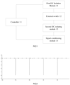
- Fig. 1 is a structural block diagram of a switch detection circuit according to an embodiment of the present invention.
- the switch detection circuit includes a controller 11, an external switch 12, a first direct current (DC) isolation module 14, a second DC isolation module 15, and a signal conditioning module 13, wherein the controller 11 includes an input end, an output end, and a voltage detection end.
- DC direct current
- an output end of the controller 11 is connected to a first end of the external switch 12 via the first DC isolation module 14.
- a control end of the signal conditioning module 13 is connected to a second end of the external switch 12 via the second DC isolation module 15.
- An output end of the signal conditioning module 13 is connected to an input end of the controller 11.
- the output end of the controller 11 is configured to output a pulse signal, and transmit the pulse signal to the second DC isolation module 15 via the first DC isolation module 14 and the external switch 12.
- the pulse signal refers to an electrical signal continuously emitted according to a certain voltage amplitude and time interval.
- the pulse signal includes but is not limited to a square wave signal, and the square wave signal outputs high and low levels at intervals, wherein, the square wave signal has rising edges and falling edges because of the jumping between high and low level in the square wave signal.
- the first DC isolation module 14 and the second DC isolation module 15 both have the property of passing alternating current (AC) and blocking DC, namely, the first DC isolation module 14 and the second DC isolation module 15 are both configured to pass AC and block DC. Specifically, the first DC isolation module 14 and the second DC isolation module 15 are also configured to isolate DC connected to the external switch 12, so as to prevent the power supply connected to the external switch 12 from interfering with the detection result or damaging components in the detection circuit.
- the current transmitted by the first DC isolation module 14 varies according to the height of the pulse signal. When the pulse signal is at a rising edge, since the first DC isolation module 14 has the characteristics of passing AC and blocking DC, and passing high frequency and blocking low frequency, the first DC isolation module 14 is equivalent to a conductive wire.
- the pulse signal flows into the external switch 12 via the first DC isolation module 14.
- the pulse signal will flow into the second DC isolation module 15 through the first DC isolation module 14.
- the level of the second DC isolation module 15 jumps, and the second DC isolation module 15 is equivalent to a conductive wire so that the pulse signal flows out from the first DC isolation module 14 and is transmitted to a control end of the signal conditioning module 13 via the second DC isolation module 15.
- the pulse signal continuously outputs the high-level signal to the first DC isolation module 14, the first DC isolation module 14 starts charging.
- the external switch 12 is turned on, the first DC isolation module 14 and the second DC isolation module 15 are equivalent to energy storage devices, and no current flows out from the first DC isolation module 14 and the second DC isolation module 15.
- the first DC isolation module 14 When the pulse signal is at a falling edge or a low-level signal, the first DC isolation module 14 is in an open circuit state, no current flows out in the first DC isolation module 14, and in turn, no current is transmitted to the signal conditioning module 13 via the second DC isolation module 15 regardless of the working state of the external switch 12.
- the electrical signal output by the second DC isolation module 15 is a current signal actually output by the second DC isolation module 15 when the controller outputs a pulse signal.
- the first DC isolation module 14 is a capacitor C1
- the second DC isolation module 15 is a capacitor C2.
- a first end of the capacitor C1 is connected to the output end of the controller 11, and a second end of the capacitor C1 is connected to the first end of the external switch 12.
- the second end of the external switch 12 is connected to a first end of the capacitor C2, and a second end of the capacitor C2 is connected to the control end of the signal conditioning module 13.
- the capacitor C1 and capacitor C2 are isolation capacitors, and have the functions of passing AC and blocking DC, and passing high frequency and blocking low frequency. Under a high-frequency signal, the capacitors C1 and C2 exhibit a low impedance characteristic, that is to say, when a pulse signal output by the output end of the controller 11 is at a rising edge, the capacitor C1 exhibits the low impedance characteristic, and the pulse signal can directly flow out through the capacitor C1.
- the external switch 12 is turned on, the pulse signal flows into the capacitor C2 through the external switch 12, and the capacitor C2 also has a current flowing out. If the external switch 12 is in an off state, no current flows out of the capacitor C2.
- the pulse signal flows into the capacitor C1 to start charging the capacitor C1, and no current flows out from the capacitor C1. At this moment, no current exists in the capacitor C2 regardless of whether the external switch 12 is turned on.
- the capacitor has a high impedance characteristic. The pulse signal is isolated by the capacitor C1, so no current flows out of the capacitor C1. At this moment, no current exists in the capacitor C2 regardless of whether the external switch 12 is turned on.
- the external switch is usually connected to a DC power supply provided by a battery.
- a switch on/off detection circuit provided in the present invention can effectively isolate the DC power supply connected to the external switch by providing capacitors C1 and C2, so as to avoid the DC power supply interfering with the detection result, and better protect the detection circuit.
- the signal conditioning module 13 is configured to output a feedback signal to the input end of the controller 11 according to the electrical signal output by the second DC isolation module 15.
- the controller 11 is also configured to count the received feedback signal to obtain a count value, and detect the working state of the external switch 12 according to the count value.
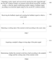
- Fig. 2 is a schematic diagram of pulse counting in a switch detection circuit according to an embodiment of the present invention.
- the vertical axis of the pulse count is the voltage value of the pulse signal and the horizontal axis is time.
- the counting refers to counting the number of times a low-level signal is received at the input end of the controller 11 over a period of time.
- the selected time period is any time period for outputting pulse signals, and the specific time period can be set by a user according to requirements.
- the signal conditioning module 13 includes a switch tube Q1 and a resistor R2.
- a control end of the switch tube Q1 is connected to a second end of the capacitor C2.
- a first end of the switch tube Q1 is connected to the input end of the controller 11 and a second end of the resistor R2.
- a second end of the switch tube Q1 is configured to be grounded.
- a first end of the resistor R2 is configured to be connected to a power supply.
- the switch tube Q1 when a current flows out of the capacitor C2, the current flows into the control end of the switch tube Q1, and in turn, the switch tube Q1 is turned on. The input end of the controller 11 is grounded via the switch tube Q1 so as to receive a low-level signal. When no current flows out of the capacitor C2, the switch Q1 is in a cut-off state, and the input end of the controller 11 is connected to the power supply via the resistor R2 so as to receive a high-level signal.
- the controller 11 is configured to judge whether the count value is greater than a preset count threshold value. When the count value is greater than the preset count threshold value, it is judged that the external switch 12 is in an on state, and when the count value is less than the preset count threshold value, it is judged that the external switch 12 is in an off state. In this way, detection of the switch state can be achieved, and the introduction of a preset count threshold value can reduce misjudgment. Further, the controller 11 is configured to count according to the number of low-level signals received at its input end, record the count value, and compare the count value with the size of a preset threshold value.
- the preset count threshold is related to the number of pulses of the output pulse signal, and the preset count threshold value is equal to or slightly smaller than the number of pulses of the pulse signal.
- the number of pulses output by the output end of the controller 11 in a period of time is equal to the number of low levels received by the input end of the controller 11, wherein the number of pulses can be understood as the number of rising edges of the pulse signal, and the number of low levels received can be understood as the count value.
- the preset count threshold value is used as a determination basis, which can improve the accuracy of on/off detection of the switch and reduce misjudgment.
- the switch detection circuit may also determine whether the external switch 12 has a fault by detecting the resistance value of the external switch 12.
- Fig. 3 is a circuit diagram of a switch detection circuit according to an embodiment of the present invention.
- the switch detection circuit further includes a resistor R1 and a resistor R3.
- a first end of the resistor R1 is connected to the output end of the controller 11, and a second end of the resistor R1 is respectively connected to the first end of the capacitor C1 and a voltage detection end of the controller 11.
- a first end of the resistor R3 is connected to the second end of the capacitor C2, and a second end of the resistor R3 is configured to be grounded.
- the sampled voltage across the second end of the resistor R1 i.e. the sum of the resistor R3 and the voltage on the external switch 12
- the voltage detection end of the controller 11 the sampled voltage across the second end of the resistor R1
- the resistor R3 the voltage on the external switch 12
- the resistance value on the external switch 12 is calculated according to the sum of the voltages. Whether the external switch 12 has a fault is determined according to the size of the resistance value.
- An embodiment of the present invention provides a switch detection circuit, wherein the switch detection circuit includes a controller, a first DC isolation module, a second DC isolation module and a signal conditioning module.
- An output end of the controller is connected to a first end of the external switch via the first DC isolation module.
- a control end of the signal conditioning module is connected to a second end of the external switch via the second DC isolation module.
- An output end of the signal conditioning module is connected to the input end of the controller.
- the output end of the controller is configured to output a pulse signal, and transmit the pulse signal to the second DC isolation module via the first DC isolation module and the external switch; at this moment, if a current flows out from the second DC isolation module, the control end of the signal conditioning module outputs a feedback signal to the input end of the controller after receiving the current, and the controller counts according to the feedback signal and detects the working state of the external switch according to the count value, so that the on/off of the external switch can be detected without using an optical coupling DC isolation module, thus reducing the circuit detection cost.
- Fig. 4 is a circuit diagram of another switch detection circuit according to an embodiment of the present invention.
- the switch detection circuit when a first end of the external switch is connected to a DC power supply, the switch detection circuit further includes a Zener diode D1.
- a cathode of the Zener diode D1 is connected to the control end of the switch tube Q1, and an anode of the Zener diode D1 is configured to be grounded.
- the capacitor C2 has the characteristics of passing AC and blocking DC and passing high frequency and blocking low frequency, the capacitor C2 is equivalent to a conductive wire at the moment when the external switch 12 is closed.
- Fig. 5 is a circuit diagram of another switch detection circuit according to an embodiment of the present invention.
- the switch detection circuit when a second end of the external switch is connected to a DC power supply, the switch detection circuit further includes a Zener diode D2.
- a cathode of the Zener diode D2 is connected to a second end of the resistor R1, and an anode of the Zener diode D2 is configured to be grounded.
- the capacitor C1 has the characteristics of passing AC and blocking DC and passing high frequency and blocking low frequency, the capacitor C1 is equivalent to a conductive wire at the moment when the external switch 12 is closed.
- Fig. 6 is a circuit diagram of yet another switch detection circuit according to an embodiment of the present invention.
- the switch detection circuit further includes Zener diodes DI and D2.
- a cathode of the Zener diode D1 is connected to the control end of the switch tube Q1, an anode of the Zener diode D1 is configured to be grounded.
- a cathode of the Zener diode D2 is connected to the second end of the resistor R1, and an anode of the Zener diode D2 is configured to be grounded.
- the capacitor C1 and the capacitor C2 are equivalent to conductive wires at the moment when the external switch 12 is closed.
- a second end of the resistor R1 is connected to the Zener diode D2 and the control end of the switch tube Q1 is connected to the Zener diode D1, so that the current in the DC power supply can directly flow out through the Zener diode, thereby avoiding misjudgment.
- Fig. 7 is a flowchart of a switch detection method according to an embodiment of the present invention, wherein the switch detection method is applied to the above-mentioned switch detection circuit.
- the switch detection method includes the following steps:
- the pulse signal is periodically outputted through the output end of the controller.
- the pulse signal refers to an electrical signal continuously emitted according to a certain voltage amplitude and time interval.
- the pulse signal includes but is not limited to, a square wave signal, and the square wave signal outputs high and low levels at intervals, wherein, the square wave signal has rising edges and falling edges because of the jumping between the high and low-level in the square wave signal.
- the current in the first DC isolation module and the second DC isolation module change according to the level of the pulse signal.
- the pulse signal is at a rising edge, the first DC isolation module is in a short-circuit state, equivalent to a conductive wire.
- the pulse signal flows out to a control end of the signal conditioning module via the first DC isolation module, the external switch, and the second DC isolation module.
- the pulse signal is at a high level
- the first DC isolation module starts charging.
- the external switch is in an on-state
- the first DC isolation module and the second DC isolation module are equivalent to energy storage devices, and no current flows out from the first DC isolation module and the second DC isolation module.
- the pulse signal is at a falling edge or a low-level signal, the first DC isolation module and the second DC isolation module are in an open circuit state, and no current flows out in the first DC isolation module and the second DC isolation module.
- the signal conditioning module when a current flows out from the second DC isolation module, the current directly flows into the control end of the signal conditioning module so as to control the signal conditioning module to be turned on. At this moment, the input end of the controller is connected to a ground end through the signal conditioning module, namely, the input end of the controller receives a low-level signal.
- the signal conditioning module When no current flows out in the second DC isolation module, the signal conditioning module is in a cut-off state, and the input end of the controller is connected to the power supply via the signal conditioning module, namely, the input end of the controller receives the high-level signal.
- the feedback signal means that the received level signal jumps from a low level to a high level, namely, if the input end of the controller receives a low-level signal and then receives a high-level signal, the controller performs counting.
- Fig. 2 is a schematic diagram of pulse counting in a switch detection circuit according to an embodiment of the present invention.
- the counting refers to counting the number of times a low-level signal is received at the input end of the controller over a period of time.
- the selected time period is any time period for outputting pulse signals, and the specific time period can be set by a user according to requirements.
- the controller counts according to the jump of the level signal, records the count value and compares the size of the count value with a preset threshold value. Wherein when the count value is greater than the preset count threshold value, it is judged that the external switch is in an on state, and when the count value is less than the preset count threshold value, it is judged that the external switch is in an off state. In this way, detection of the switch state can be achieved, and the introduction of a preset count threshold value can reduce misjudgment.
- the switch detection method further includes determining whether the external switch has a fault.
- Fig. 8 is a flowchart of external switch fault detection in a switch detection method according to an embodiment of the present invention. As shown in Fig. 8 , the switch detection method includes: S11 acquiring a sampled voltage at the rising edge of the pulse signal.
- the sampled voltage refers to the voltage collected at the voltage detection terminal of the controller when the rising edge of the pulse signal is output at the output end of the controller, that is, the sum of the voltage of the external switch and the voltage of the resistor R3.
- the acquisition mode of the sampled voltage may also include: acquiring a voltage value across the resistor R1, then acquiring the voltage value of the pulse signal, subtracting the voltage value of the resistor R1 from the voltage value of the pulse signal to obtain a difference, i.e. the voltage value of the sampled voltage.
- the resistance value of the external switch is calculated according to the sampled voltage.
- the resistance value of the external switch is calculated and the magnitude of the resistance value of the external switch is judged. If the resistance value of the external switch is less than a first preset resistance value, then the external switch is in a normally conductive state; and if the resistance value of the external switch is greater than the first preset resistance value and less than a second preset resistance value, then the external switch is in a fault conductive state. When the external switch is in a cut-off state, the resistance value of the external switch is calculated and the magnitude of the resistance value of the external switch is judged.
- the external switch is in a normal cut-off or fault cut-off or a second end short-circuit cut-off state. If the sampled voltage gradually rises to the pulse signal voltage value, the external switch is in a first end short-circuit cut-off state and/or a first end short-circuit conductive state and/or a second end short-circuit conductive state.
- the first preset resistance value may be set to zero and the second preset resistance value may be set to infinity.
- the embodiment of the present invention provides a switch detection method, which includes: outputting a pulse signal, and sequentially passing the pulse signal through the first DC isolation module, the external switch, and the second DC isolation module, so that the signal conditioning module outputs a feedback signal according to the electrical signal output by the second DC isolation module, then counting according to the signal fed back by the signal conditioning module to obtain a count value, and finally detecting the working state of the external switch according to the count value.
- the switch detection method includes: outputting a pulse signal, and sequentially passing the pulse signal through the first DC isolation module, the external switch, and the second DC isolation module, so that the signal conditioning module outputs a feedback signal according to the electrical signal output by the second DC isolation module, then counting according to the signal fed back by the signal conditioning module to obtain a count value, and finally detecting the working state of the external switch according to the count value.
- Embodiments of the present invention also provide a switch detector comprising the above-mentioned switch detection circuit and/or switch detection method.
- the switch detector outputs a pulse signal via an output end of a controller, then an input end of the controller receives a feedback signal and counts.
- the on/off of the switch can be judged via the count value, thereby avoiding the use of an optical coupling DC isolation module for detection, reducing the cost of the circuit.
- the resistance value of the switch is detected via a voltage detection end of the controller, so that the switch detector can judge whether the switch has a fault while detecting the on/off of the switch.
Landscapes
- Engineering & Computer Science (AREA)
- Power Engineering (AREA)
- Manufacturing & Machinery (AREA)
- Chemical & Material Sciences (AREA)
- Chemical Kinetics & Catalysis (AREA)
- Electrochemistry (AREA)
- General Chemical & Material Sciences (AREA)
- Physics & Mathematics (AREA)
- General Physics & Mathematics (AREA)
- Electronic Switches (AREA)
- Testing Electric Properties And Detecting Electric Faults (AREA)
- Keying Circuit Devices (AREA)
Applications Claiming Priority (1)
| Application Number | Priority Date | Filing Date | Title |
|---|---|---|---|
| CN202210165686.4A CN114217220B (zh) | 2022-02-23 | 2022-02-23 | 一种开关检测电路、方法及开关检测器 |
Publications (3)
| Publication Number | Publication Date |
|---|---|
| EP4235196A1 true EP4235196A1 (de) | 2023-08-30 |
| EP4235196B1 EP4235196B1 (de) | 2024-08-21 |
| EP4235196C0 EP4235196C0 (de) | 2024-08-21 |
Family
ID=80709343
Family Applications (1)
| Application Number | Title | Priority Date | Filing Date |
|---|---|---|---|
| EP22200359.2A Active EP4235196B1 (de) | 2022-02-23 | 2022-10-07 | Schaltererkennungsschaltung, verfahren und schalterdetektor |
Country Status (4)
| Country | Link |
|---|---|
| US (1) | US11695284B1 (de) |
| EP (1) | EP4235196B1 (de) |
| JP (1) | JP7303359B1 (de) |
| CN (1) | CN114217220B (de) |
Families Citing this family (3)
| Publication number | Priority date | Publication date | Assignee | Title |
|---|---|---|---|---|
| CN117269758B (zh) * | 2023-09-19 | 2025-04-29 | 青岛海洋科技中心 | 电机滑环定子导线与转子导线通断测试装置及测试方法 |
| CN119178950B (zh) * | 2024-11-25 | 2025-04-01 | 四川泛华航空仪表电器有限公司 | 一种航空发动机点火装置的状态监测系统及方法 |
| CN119335384B (zh) * | 2024-12-23 | 2025-05-20 | 济宁鲁科检测科技有限公司 | 应用于磁粉探伤仪的工作开关检测电路及其判断方法 |
Citations (5)
| Publication number | Priority date | Publication date | Assignee | Title |
|---|---|---|---|---|
| CN106569128A (zh) * | 2016-11-03 | 2017-04-19 | 宁德时代新能源科技股份有限公司 | 一种检测方法和装置 |
| CN207488457U (zh) * | 2017-11-20 | 2018-06-12 | 深圳市蓝海华腾技术股份有限公司 | 一种高压直流接触器通断检测系统 |
| CN209765017U (zh) * | 2019-04-03 | 2019-12-10 | 福建金闽再造烟叶发展有限公司 | 继电器检测装置及烟草薄片生产系统 |
| CN111220930A (zh) * | 2018-11-23 | 2020-06-02 | 上海海拉电子有限公司 | 一种电动汽车接触器、熔断器通断状态的检测装置及方法 |
| CN111913132A (zh) * | 2020-06-22 | 2020-11-10 | 南京康尼电子科技有限公司 | 一种回路通断状态检测装置及方法 |
Family Cites Families (10)
| Publication number | Priority date | Publication date | Assignee | Title |
|---|---|---|---|---|
| JPH07212969A (ja) * | 1994-01-25 | 1995-08-11 | Amada Co Ltd | 電源装置の突入電流防止回路 |
| EP2149826B1 (de) | 2008-08-01 | 2011-11-30 | Siemens Aktiengesellschaft | Sicherheitsschaltanordnung zur Ausgabe eines Schaltsignals |
| JP5910172B2 (ja) * | 2012-03-01 | 2016-04-27 | 株式会社Gsユアサ | スイッチ故障診断装置、電池パックおよびスイッチ故障診断プログラム、スイッチ故障診断方法 |
| CN203965585U (zh) * | 2014-06-18 | 2014-11-26 | 深圳市沃泰克环保设备有限公司 | 一种高压开关检测装置 |
| KR102051177B1 (ko) * | 2016-10-19 | 2019-12-17 | 주식회사 엘지화학 | 전압 분배를 이용한 스위치 진단 장치 및 방법 |
| CN206557343U (zh) * | 2017-02-28 | 2017-10-13 | 国家电网公司 | 一种基于正交脉冲测量断路器分合闸时间的装置 |
| CN107179500B (zh) * | 2017-06-19 | 2020-06-02 | 国家电网公司 | 基于正交脉冲的断路器两端接地时测量分合闸时间的方法 |
| CN107976626B (zh) * | 2017-11-16 | 2019-12-06 | 湖南工业大学 | 继电器寿命检测装置 |
| CN109814017A (zh) * | 2017-11-20 | 2019-05-28 | 国网上海市电力公司 | 三相换相开关的igbt通断状态检测电路及其检测方法和应用 |
| KR102412313B1 (ko) * | 2018-07-17 | 2022-06-22 | 주식회사 엘지에너지솔루션 | 스위치 진단 장치 및 방법 |
-
2022
- 2022-02-23 CN CN202210165686.4A patent/CN114217220B/zh active Active
- 2022-09-14 US US17/944,350 patent/US11695284B1/en active Active
- 2022-09-16 JP JP2022148473A patent/JP7303359B1/ja active Active
- 2022-10-07 EP EP22200359.2A patent/EP4235196B1/de active Active
Patent Citations (5)
| Publication number | Priority date | Publication date | Assignee | Title |
|---|---|---|---|---|
| CN106569128A (zh) * | 2016-11-03 | 2017-04-19 | 宁德时代新能源科技股份有限公司 | 一种检测方法和装置 |
| CN207488457U (zh) * | 2017-11-20 | 2018-06-12 | 深圳市蓝海华腾技术股份有限公司 | 一种高压直流接触器通断检测系统 |
| CN111220930A (zh) * | 2018-11-23 | 2020-06-02 | 上海海拉电子有限公司 | 一种电动汽车接触器、熔断器通断状态的检测装置及方法 |
| CN209765017U (zh) * | 2019-04-03 | 2019-12-10 | 福建金闽再造烟叶发展有限公司 | 继电器检测装置及烟草薄片生产系统 |
| CN111913132A (zh) * | 2020-06-22 | 2020-11-10 | 南京康尼电子科技有限公司 | 一种回路通断状态检测装置及方法 |
Also Published As
| Publication number | Publication date |
|---|---|
| EP4235196B1 (de) | 2024-08-21 |
| CN114217220B (zh) | 2022-05-17 |
| JP7303359B1 (ja) | 2023-07-04 |
| US11695284B1 (en) | 2023-07-04 |
| JP2023122615A (ja) | 2023-09-04 |
| CN114217220A (zh) | 2022-03-22 |
| EP4235196C0 (de) | 2024-08-21 |
Similar Documents
| Publication | Publication Date | Title |
|---|---|---|
| EP4235196A1 (de) | Schaltererkennungsschaltung, verfahren und schalterdetektor | |
| EP1930737B1 (de) | Detektionsvorrichtung für den isolationswiderstand | |
| EP3598150B1 (de) | Isolierungsdetektionsvorrichtung und verfahren für ein energiespeichersystem | |
| EP2135105B1 (de) | Überwachungssystem der batteriespannung | |
| EP2564485B1 (de) | Detektionsverfahren und -systeme für das vorhandensein einer batterie | |
| CN107167690B (zh) | 一种电池组电压采集系统断线检测装置和方法 | |
| EP3779475B1 (de) | Isolationserkennungsschaltung und isolationserkennungsverfahren | |
| US11469453B2 (en) | Open cell detection systems and methods | |
| EP3832332A1 (de) | Hochspannungsverriegelungsschaltung und detektionsverfahren | |
| CN104569597A (zh) | 动力电池的绝缘电阻的检测方法和装置 | |
| WO2025077373A1 (zh) | 漏液检测电路、系统、方法、装置、设备及电池管理系统 | |
| CN111239469B (zh) | 冲击信号检测电路与交流供电设备 | |
| EP4697543A1 (de) | Wechselrichter zur speicherung von fotovoltaischer energie und steuerungsverfahren dafür | |
| EP4283316A1 (de) | Detektionsschaltung, rückflussverhinderungssystem und ladesäule | |
| US9836558B2 (en) | Electrical system mapping utilizing plug-in modules | |
| CN210199213U (zh) | 占空比转换电路、检测装置及安全气囊检测系统 | |
| CN220368610U (zh) | 一种电压转换电路及电压转换装置 | |
| CN115575806B (zh) | 一种动力电池系统状态检测装置及方法 | |
| CN215415698U (zh) | 一种薄膜电容性能测试装置 | |
| CN205911778U (zh) | 串联电池的均衡充电电路及其装置 | |
| CN116160861A (zh) | 一种绝缘监测装置、绝缘监测装置的控制方法和电动汽车 | |
| CN210222114U (zh) | 零点检测装置及系统 | |
| CN116125342B (zh) | 直流电的谐波检测系统、方法、装置及存储介质 | |
| CN216748022U (zh) | 用于隔离电源的隔离检测电路 | |
| CN217486199U (zh) | 用于电池包的监控设备 |
Legal Events
| Date | Code | Title | Description |
|---|---|---|---|
| PUAI | Public reference made under article 153(3) epc to a published international application that has entered the european phase |
Free format text: ORIGINAL CODE: 0009012 |
|
| STAA | Information on the status of an ep patent application or granted ep patent |
Free format text: STATUS: REQUEST FOR EXAMINATION WAS MADE |
|
| 17P | Request for examination filed |
Effective date: 20221007 |
|
| AK | Designated contracting states |
Kind code of ref document: A1 Designated state(s): AL AT BE BG CH CY CZ DE DK EE ES FI FR GB GR HR HU IE IS IT LI LT LU LV MC ME MK MT NL NO PL PT RO RS SE SI SK SM TR |
|
| GRAP | Despatch of communication of intention to grant a patent |
Free format text: ORIGINAL CODE: EPIDOSNIGR1 |
|
| STAA | Information on the status of an ep patent application or granted ep patent |
Free format text: STATUS: GRANT OF PATENT IS INTENDED |
|
| INTG | Intention to grant announced |
Effective date: 20240506 |
|
| RIC1 | Information provided on ipc code assigned before grant |
Ipc: H01H 9/02 20060101ALI20240422BHEP Ipc: G01R 31/327 20060101AFI20240422BHEP |
|
| GRAS | Grant fee paid |
Free format text: ORIGINAL CODE: EPIDOSNIGR3 |
|
| GRAA | (expected) grant |
Free format text: ORIGINAL CODE: 0009210 |
|
| STAA | Information on the status of an ep patent application or granted ep patent |
Free format text: STATUS: THE PATENT HAS BEEN GRANTED |
|
| AK | Designated contracting states |
Kind code of ref document: B1 Designated state(s): AL AT BE BG CH CY CZ DE DK EE ES FI FR GB GR HR HU IE IS IT LI LT LU LV MC ME MK MT NL NO PL PT RO RS SE SI SK SM TR |
|
| REG | Reference to a national code |
Ref country code: GB Ref legal event code: FG4D |
|
| REG | Reference to a national code |
Ref country code: CH Ref legal event code: EP |
|
| REG | Reference to a national code |
Ref country code: DE Ref legal event code: R096 Ref document number: 602022005464 Country of ref document: DE |
|
| REG | Reference to a national code |
Ref country code: IE Ref legal event code: FG4D |
|
| U01 | Request for unitary effect filed |
Effective date: 20240905 |
|
| U07 | Unitary effect registered |
Designated state(s): AT BE BG DE DK EE FI FR IT LT LU LV MT NL PT RO SE SI Effective date: 20240923 |
|
| U20 | Renewal fee for the european patent with unitary effect paid |
Year of fee payment: 3 Effective date: 20240927 |
|
| PG25 | Lapsed in a contracting state [announced via postgrant information from national office to epo] |
Ref country code: NO Free format text: LAPSE BECAUSE OF FAILURE TO SUBMIT A TRANSLATION OF THE DESCRIPTION OR TO PAY THE FEE WITHIN THE PRESCRIBED TIME-LIMIT Effective date: 20241121 |
|
| PG25 | Lapsed in a contracting state [announced via postgrant information from national office to epo] |
Ref country code: GR Free format text: LAPSE BECAUSE OF FAILURE TO SUBMIT A TRANSLATION OF THE DESCRIPTION OR TO PAY THE FEE WITHIN THE PRESCRIBED TIME-LIMIT Effective date: 20241122 Ref country code: PL Free format text: LAPSE BECAUSE OF FAILURE TO SUBMIT A TRANSLATION OF THE DESCRIPTION OR TO PAY THE FEE WITHIN THE PRESCRIBED TIME-LIMIT Effective date: 20240821 |
|
| PG25 | Lapsed in a contracting state [announced via postgrant information from national office to epo] |
Ref country code: IS Free format text: LAPSE BECAUSE OF FAILURE TO SUBMIT A TRANSLATION OF THE DESCRIPTION OR TO PAY THE FEE WITHIN THE PRESCRIBED TIME-LIMIT Effective date: 20241221 |
|
| PG25 | Lapsed in a contracting state [announced via postgrant information from national office to epo] |
Ref country code: HR Free format text: LAPSE BECAUSE OF FAILURE TO SUBMIT A TRANSLATION OF THE DESCRIPTION OR TO PAY THE FEE WITHIN THE PRESCRIBED TIME-LIMIT Effective date: 20240821 |
|
| PG25 | Lapsed in a contracting state [announced via postgrant information from national office to epo] |
Ref country code: ES Free format text: LAPSE BECAUSE OF FAILURE TO SUBMIT A TRANSLATION OF THE DESCRIPTION OR TO PAY THE FEE WITHIN THE PRESCRIBED TIME-LIMIT Effective date: 20240821 Ref country code: RS Free format text: LAPSE BECAUSE OF FAILURE TO SUBMIT A TRANSLATION OF THE DESCRIPTION OR TO PAY THE FEE WITHIN THE PRESCRIBED TIME-LIMIT Effective date: 20241121 |
|
| PG25 | Lapsed in a contracting state [announced via postgrant information from national office to epo] |
Ref country code: RS Free format text: LAPSE BECAUSE OF FAILURE TO SUBMIT A TRANSLATION OF THE DESCRIPTION OR TO PAY THE FEE WITHIN THE PRESCRIBED TIME-LIMIT Effective date: 20241121 Ref country code: PL Free format text: LAPSE BECAUSE OF FAILURE TO SUBMIT A TRANSLATION OF THE DESCRIPTION OR TO PAY THE FEE WITHIN THE PRESCRIBED TIME-LIMIT Effective date: 20240821 Ref country code: NO Free format text: LAPSE BECAUSE OF FAILURE TO SUBMIT A TRANSLATION OF THE DESCRIPTION OR TO PAY THE FEE WITHIN THE PRESCRIBED TIME-LIMIT Effective date: 20241121 Ref country code: IS Free format text: LAPSE BECAUSE OF FAILURE TO SUBMIT A TRANSLATION OF THE DESCRIPTION OR TO PAY THE FEE WITHIN THE PRESCRIBED TIME-LIMIT Effective date: 20241221 Ref country code: HR Free format text: LAPSE BECAUSE OF FAILURE TO SUBMIT A TRANSLATION OF THE DESCRIPTION OR TO PAY THE FEE WITHIN THE PRESCRIBED TIME-LIMIT Effective date: 20240821 Ref country code: GR Free format text: LAPSE BECAUSE OF FAILURE TO SUBMIT A TRANSLATION OF THE DESCRIPTION OR TO PAY THE FEE WITHIN THE PRESCRIBED TIME-LIMIT Effective date: 20241122 Ref country code: ES Free format text: LAPSE BECAUSE OF FAILURE TO SUBMIT A TRANSLATION OF THE DESCRIPTION OR TO PAY THE FEE WITHIN THE PRESCRIBED TIME-LIMIT Effective date: 20240821 |
|
| PG25 | Lapsed in a contracting state [announced via postgrant information from national office to epo] |
Ref country code: SM Free format text: LAPSE BECAUSE OF FAILURE TO SUBMIT A TRANSLATION OF THE DESCRIPTION OR TO PAY THE FEE WITHIN THE PRESCRIBED TIME-LIMIT Effective date: 20240821 |
|
| PG25 | Lapsed in a contracting state [announced via postgrant information from national office to epo] |
Ref country code: CZ Free format text: LAPSE BECAUSE OF FAILURE TO SUBMIT A TRANSLATION OF THE DESCRIPTION OR TO PAY THE FEE WITHIN THE PRESCRIBED TIME-LIMIT Effective date: 20240821 |
|
| PG25 | Lapsed in a contracting state [announced via postgrant information from national office to epo] |
Ref country code: SK Free format text: LAPSE BECAUSE OF FAILURE TO SUBMIT A TRANSLATION OF THE DESCRIPTION OR TO PAY THE FEE WITHIN THE PRESCRIBED TIME-LIMIT Effective date: 20240821 |
|
| PLBE | No opposition filed within time limit |
Free format text: ORIGINAL CODE: 0009261 |
|
| STAA | Information on the status of an ep patent application or granted ep patent |
Free format text: STATUS: NO OPPOSITION FILED WITHIN TIME LIMIT |
|
| PG25 | Lapsed in a contracting state [announced via postgrant information from national office to epo] |
Ref country code: MC Free format text: LAPSE BECAUSE OF FAILURE TO SUBMIT A TRANSLATION OF THE DESCRIPTION OR TO PAY THE FEE WITHIN THE PRESCRIBED TIME-LIMIT Effective date: 20240821 |
|
| 26N | No opposition filed |
Effective date: 20250522 |
|
| PG25 | Lapsed in a contracting state [announced via postgrant information from national office to epo] |
Ref country code: IE Free format text: LAPSE BECAUSE OF NON-PAYMENT OF DUE FEES Effective date: 20241007 |
|
| U20 | Renewal fee for the european patent with unitary effect paid |
Year of fee payment: 4 Effective date: 20250926 |
|
| U1N | Appointed representative for the unitary patent procedure changed after the registration of the unitary effect |
Representative=s name: SANTARELLI; FR |
|
| PG25 | Lapsed in a contracting state [announced via postgrant information from national office to epo] |
Ref country code: CY Free format text: LAPSE BECAUSE OF FAILURE TO SUBMIT A TRANSLATION OF THE DESCRIPTION OR TO PAY THE FEE WITHIN THE PRESCRIBED TIME-LIMIT; INVALID AB INITIO Effective date: 20221007 |
|
| PG25 | Lapsed in a contracting state [announced via postgrant information from national office to epo] |
Ref country code: HU Free format text: LAPSE BECAUSE OF FAILURE TO SUBMIT A TRANSLATION OF THE DESCRIPTION OR TO PAY THE FEE WITHIN THE PRESCRIBED TIME-LIMIT; INVALID AB INITIO Effective date: 20221007 |