EP4231360A1 - Hemt device having low conduction losses and manufacturing process thereof - Google Patents
Hemt device having low conduction losses and manufacturing process thereof Download PDFInfo
- Publication number
- EP4231360A1 EP4231360A1 EP23156230.7A EP23156230A EP4231360A1 EP 4231360 A1 EP4231360 A1 EP 4231360A1 EP 23156230 A EP23156230 A EP 23156230A EP 4231360 A1 EP4231360 A1 EP 4231360A1
- Authority
- EP
- European Patent Office
- Prior art keywords
- wafer
- manufacturing process
- silicon carbide
- hemt device
- substrate
- Prior art date
- Legal status (The legal status is an assumption and is not a legal conclusion. Google has not performed a legal analysis and makes no representation as to the accuracy of the status listed.)
- Pending
Links
Images


Classifications
-
- H—ELECTRICITY
- H10—SEMICONDUCTOR DEVICES; ELECTRIC SOLID-STATE DEVICES NOT OTHERWISE PROVIDED FOR
- H10D—INORGANIC ELECTRIC SEMICONDUCTOR DEVICES
- H10D30/00—Field-effect transistors [FET]
- H10D30/40—FETs having zero-dimensional [0D], one-dimensional [1D] or two-dimensional [2D] charge carrier gas channels
- H10D30/47—FETs having zero-dimensional [0D], one-dimensional [1D] or two-dimensional [2D] charge carrier gas channels having two-dimensional [2D] charge carrier gas channels, e.g. nanoribbon FETs or high electron mobility transistors [HEMT]
- H10D30/471—High electron mobility transistors [HEMT] or high hole mobility transistors [HHMT]
- H10D30/475—High electron mobility transistors [HEMT] or high hole mobility transistors [HHMT] having wider bandgap layer formed on top of lower bandgap active layer, e.g. undoped barrier HEMTs such as i-AlGaN/GaN HEMTs
-
- H—ELECTRICITY
- H10—SEMICONDUCTOR DEVICES; ELECTRIC SOLID-STATE DEVICES NOT OTHERWISE PROVIDED FOR
- H10D—INORGANIC ELECTRIC SEMICONDUCTOR DEVICES
- H10D30/00—Field-effect transistors [FET]
- H10D30/01—Manufacture or treatment
- H10D30/015—Manufacture or treatment of FETs having heterojunction interface channels or heterojunction gate electrodes, e.g. HEMT
-
- H—ELECTRICITY
- H10—SEMICONDUCTOR DEVICES; ELECTRIC SOLID-STATE DEVICES NOT OTHERWISE PROVIDED FOR
- H10D—INORGANIC ELECTRIC SEMICONDUCTOR DEVICES
- H10D30/00—Field-effect transistors [FET]
- H10D30/40—FETs having zero-dimensional [0D], one-dimensional [1D] or two-dimensional [2D] charge carrier gas channels
- H10D30/47—FETs having zero-dimensional [0D], one-dimensional [1D] or two-dimensional [2D] charge carrier gas channels having two-dimensional [2D] charge carrier gas channels, e.g. nanoribbon FETs or high electron mobility transistors [HEMT]
- H10D30/471—High electron mobility transistors [HEMT] or high hole mobility transistors [HHMT]
- H10D30/475—High electron mobility transistors [HEMT] or high hole mobility transistors [HHMT] having wider bandgap layer formed on top of lower bandgap active layer, e.g. undoped barrier HEMTs such as i-AlGaN/GaN HEMTs
- H10D30/4755—High electron mobility transistors [HEMT] or high hole mobility transistors [HHMT] having wider bandgap layer formed on top of lower bandgap active layer, e.g. undoped barrier HEMTs such as i-AlGaN/GaN HEMTs having wide bandgap charge-carrier supplying layers, e.g. modulation doped HEMTs such as n-AlGaAs/GaAs HEMTs
-
- H—ELECTRICITY
- H10—SEMICONDUCTOR DEVICES; ELECTRIC SOLID-STATE DEVICES NOT OTHERWISE PROVIDED FOR
- H10D—INORGANIC ELECTRIC SEMICONDUCTOR DEVICES
- H10D62/00—Semiconductor bodies, or regions thereof, of devices having potential barriers
- H10D62/80—Semiconductor bodies, or regions thereof, of devices having potential barriers characterised by the materials
- H10D62/83—Semiconductor bodies, or regions thereof, of devices having potential barriers characterised by the materials being Group IV materials, e.g. B-doped Si or undoped Ge
- H10D62/832—Semiconductor bodies, or regions thereof, of devices having potential barriers characterised by the materials being Group IV materials, e.g. B-doped Si or undoped Ge being Group IV materials comprising two or more elements, e.g. SiGe
- H10D62/8325—Silicon carbide
-
- H—ELECTRICITY
- H10—SEMICONDUCTOR DEVICES; ELECTRIC SOLID-STATE DEVICES NOT OTHERWISE PROVIDED FOR
- H10P—GENERIC PROCESSES OR APPARATUS FOR THE MANUFACTURE OR TREATMENT OF DEVICES COVERED BY CLASS H10
- H10P72/00—Handling or holding of wafers, substrates or devices during manufacture or treatment thereof
- H10P72/70—Handling or holding of wafers, substrates or devices during manufacture or treatment thereof for supporting or gripping
- H10P72/74—Handling or holding of wafers, substrates or devices during manufacture or treatment thereof for supporting or gripping using temporarily an auxiliary support
-
- H—ELECTRICITY
- H10—SEMICONDUCTOR DEVICES; ELECTRIC SOLID-STATE DEVICES NOT OTHERWISE PROVIDED FOR
- H10D—INORGANIC ELECTRIC SEMICONDUCTOR DEVICES
- H10D62/00—Semiconductor bodies, or regions thereof, of devices having potential barriers
- H10D62/80—Semiconductor bodies, or regions thereof, of devices having potential barriers characterised by the materials
- H10D62/85—Semiconductor bodies, or regions thereof, of devices having potential barriers characterised by the materials being Group III-V materials, e.g. GaAs
- H10D62/8503—Nitride Group III-V materials, e.g. AlN or GaN
-
- H—ELECTRICITY
- H10—SEMICONDUCTOR DEVICES; ELECTRIC SOLID-STATE DEVICES NOT OTHERWISE PROVIDED FOR
- H10D—INORGANIC ELECTRIC SEMICONDUCTOR DEVICES
- H10D64/00—Electrodes of devices having potential barriers
- H10D64/20—Electrodes characterised by their shapes, relative sizes or dispositions
- H10D64/23—Electrodes carrying the current to be rectified, amplified, oscillated or switched, e.g. sources, drains, anodes or cathodes
- H10D64/251—Source or drain electrodes for field-effect devices
- H10D64/256—Source or drain electrodes for field-effect devices for lateral devices wherein the source or drain electrodes are recessed in semiconductor bodies
Definitions
- the present invention relates to a high electron mobility transistor (HEMT) device having low conduction losses and to the manufacturing process thereof.
- HEMT high electron mobility transistor
- HEMT devices wherein a conductive channel is based on the formation of a two-dimensional electron gas (2DEG) having high mobility at a heterojunction, that is at the interface between semiconductor materials having different band gap.
- 2DEG two-dimensional electron gas
- HEMT devices based on the heterojunction between an aluminum gallium nitride (AlGaN) layer and a gallium nitride (GaN) layer are known.
- the HEMT devices based on AlGaN/GaN heterojunctions or heterostructures offer several advantages that make them particularly suitable and widely used for different applications. For example, the high breakdown voltage of the HEMT devices is exploited for high-performance power switches; the high mobility of the electrons in the conductive channel allows high-frequency amplifiers to be provided; in addition, the high concentration of electrons in the 2DEG allows a low ON-state resistance (R ON ) to be obtained.
- R ON ON-state resistance
- the HEMT devices for radio frequency (RF) applications typically have better RF performances with respect to similar silicon LDMOS devices.
- the heterostructure extends on a substrate.
- the substrate In order to reduce, in use, the conductive losses through the substrate, it is desired that the substrate has a high resistivity.
- the heterostructure is grown on a resistive silicon substrate.
- the Applicant has verified that the heterostructure of the known HEMT devices grown on silicon is subject to a high concentration of crystallographic defects. Consequently, the corresponding HEMT devices have low electrical performances, in use.
- the heterostructure is grown directly on a semi-insulating silicon carbide wafer.
- the semi-insulating silicon carbide wafers have a high cost, especially in the case of wafers having large dimensions, for example having a diameter of 200 mm. Consequently, the HEMT devices obtained from semi-insulating silicon carbide wafers have a high manufacturing cost.
- the aim of the present invention is to overcome the disadvantages of the prior art.
- Figure 1 shows a work body 1 comprising a wafer 2 having a front surface 2A and a back surface 2B, in a Cartesian reference system XYZ comprising a first axis X, a second axis Y and a third axis Z.
- the front surface 2A and the back surface 2B of the wafer 2 respectively form a front surface and a back surface of the work body 1.
- the wafer 2 is of silicon carbide (SiC) in one of its polytypes, for example 3C, 4H, 6H, here of the polytype 4H.
- the wafer 2 is a SiC wafer of conductive type, for example having a conductivity of n-type or p-type, here of n-type.
- the wafer 2 has a resistivity lower than 0.1 ⁇ cm, for example comprised between 0.005 ⁇ cm and 0.05 ⁇ cm.
- the wafer 2 may have a concentration of n-type doping atoms comprised between 1.10 17 atoms/cm 3 and 1-10 19 atoms/cm 3 .
- the wafer 2 has a cut angle such that the front surface 2A of the wafer 2 is tilted by a non-zero angle with respect to a C-type plane or face of the crystallographic structure of the silicon carbide.
- the front surface 2A of the wafer 2 is tilted by the cut angle with respect to the face (000-1) of the 4H-SiC, wherein the values 0, 0, 0, -1 respectively indicate the indices h, k, i, 1 of Bravais-Miller.
- the surface 2A of the wafer 2 is an off-axis face of the wafer 2, in particular having a cut angle lower than 4°.
- the surface 2A of the wafer 2 may have a different cut angle, for example equal to zero; that is, the surface 2A of the wafer 2 may be parallel to the face (000-1) of the 4H-SiC.
- the wafer 2 has a thickness T W along the third axis Z comprised for example between 100 ⁇ m and 500 ⁇ m, in particular comprised between 250 ⁇ m and 350 ⁇ m.
- the wafer 2 may have a width or diameter D, parallel to the first axis X, that is high, for example comprised between 50 mm and 200 mm.
- an epitaxial layer 4 of silicon carbide is grown on the front surface 2A of the wafer 2.
- the epitaxial layer 4 has a surface 4A and a thickness T E , along the third axis Z, comprised for example between 60 ⁇ m and 100 ⁇ m.
- the surface 4A of the epitaxial layer 4 thus forms a new front surface of the work body 1.
- the epitaxial layer 4 is formed by highly resistive silicon carbide, for example having a resistivity greater than 1 ⁇ 10 4 ⁇ cm.
- the epitaxial layer 4 has a greater resistivity than the wafer 2.
- the epitaxial layer 4 is grown so as to have a low concentration of doping atoms.
- the epitaxial layer 4 may have a concentration of doping atoms, for example of n-type such as nitrogen atoms, lower than 5.10 14 atoms/cm 3 , in particular comprised between 5 ⁇ 10 11 and 5 ⁇ 10 13 atoms/cm 3 .
- the epitaxial layer 4 may maintain the crystallographic orientation of the front surface 2A of the wafer 2. Consequently, in this embodiment, the surface 4A of the epitaxial layer 4 may maintain the same cut angle as the front surface 2A of the wafer 2.
- the crystalline structure of the epitaxial layer 4 changes as a function of the cut angle of the front surface 2A of the wafer 2.
- the fact that the epitaxial layer 4 grows epitaxially on the off-axis face of the wafer 2 may cause a step-flow growth of the epitaxial layer 4.
- the epitaxial layer 4 may thus have a terrace structure indicating said epitaxial off-axis growth.
- Said terraces may be observed through superficial morphological analysis of the epitaxial layer 4.
- a heterostructure 5 is grown on the surface 4A of the epitaxial layer 4.
- the heterostructure 5 has a surface 5A which forms a new front surface of the work body 1.
- the heterostructure 5 comprises compound semiconductor materials including elements of the group III-V.
- the heterostructure 5 is formed by a channel layer 6 of a first semiconductor material, for example gallium nitride (GaN) or an alloy comprising gallium nitride such as InGaN, here of intrinsic gallium nitride (GaN), extending on the epitaxial layer 4, and by a barrier layer 8 of a second semiconductor material, for example a compound based on a ternary or quaternary alloy of gallium nitride, such as Al x Ga 1-x N, AlInGaN, In x Ga 1-x N, Al x In 1-x Al, AlScN, here of intrinsic aluminum gallium nitride (AlGaN), extending on the channel layer 6.
- a first semiconductor material for example gallium nitride (GaN) or an alloy comprising gallium nitride such as InGaN, here of intrinsic gallium nitride (GaN)
- GaN gallium nitride
- GaN intrinsic gallium
- the channel layer 6 extends on the surface 4A of the epitaxial layer 4, in direct contact therewith.
- the barrier layer 8 extends on the channel layer 6, in direct contact therewith; the heterostructure 5 therefore comprises an interface 6A between the channel layer 6 and the barrier layer 8.
- the wafer 2 is removed.
- the wafer 2 may be removed through a thinning process such as mechanical grinding, chemical mechanical polishing (CMP) or slicing through a laser process.
- CMP chemical mechanical polishing
- the state of removal of the wafer 2 may be controlled through an electrical measurement, for example through a mercury probe C-V measurement, or through an optical measurement.
- the epitaxial layer 4 now forms the back surface, here indicated by 11, of the work body 1.
- FIG. 5 a source region 13, a drain region 15, an insulation or passivation layer 16 and a gate region 17 are formed in a per se known manner and not further described herein.
- the source region 13 and the drain region 15 are of conductive material and extend in direct electrical contact with the heterostructure 5, in particular in ohmic contact with the channel layer 6.
- the source region 13 and the drain region 15 extend in depth into the heterostructure 5, up to the interface 6A.
- the source region 13 and the drain region 15 may extend into the heterostructure 5 up to a different depth, depending on the specific application.
- the insulation layer 16 is of dielectric material, for example silicon nitride or silicon oxide and extends on the surface 5A of the heterostructure 5.
- the gate region 17 comprises conductive material and extends through the insulation layer 16, between the source region 13 and the drain region 15, in direct electrical contact with the heterostructure 5.
- the gate region 17 may be formed by a single conductive layer or by a stack of conductive layers, comprising for example gold, nickel, titanium, etc., depending on the specific application.
- the gate region 17 may be formed by an insulating layer, in direct contact with the heterostructure 5, and one or more conductive layers extending on the insulating layer, so that the one or more conductive layers are not in direct electrical contact with the heterostructure 5.
- the gate region 17 may also partially extend within the heterostructure 5, depending on the specific application.
- the work body 1 is then subject to final manufacturing steps such as dicing and electrical connection, of a per se known type, thus forming a HEMT device 50 ( Figure 6 ).
- the HEMT device 50 is particularly suitable for being used in RF applications, such as for example 4G and 5G base stations, including technology evolutions and variants, mobile phones, RF heat treatment devices, drying and heating devices, devices and systems for avionics, L- and S-band radar, and the like.
- the HEMT device 50 is formed in a body or die 55 having a back surface 57 and comprises an epitaxial substrate 4 (corresponding to the epitaxial layer 4 and therefore indicated by the same reference number) and the heterostructure 5 extending in direct contact on the epitaxial substrate 4.
- the epitaxial substrate 4 has a thickness along the third axis Z comprised, for example, between 60 ⁇ m and 100 ⁇ m, and forms the back surface 57 of the body 55.
- the back surface 57 is an external surface of the body 55, delimiting the body 55 at the back.
- the source region 13, the drain region 15 and the gate region 17 respectively form a source electrode S, a drain electrode D and a gate electrode G of the HEMT device 50.
- the body 55 accommodates an active region 60, indicated by a dashed line in Figure 6 , which accommodates, in use, a conductive channel of the HEMT device 50.
- the fact that the epitaxial substrate 4 has a low concentration of impurities and therefore a high resistivity causes the HEMT device 50 to have low conductive losses through the epitaxial substrate 4, especially in radiofrequency applications.
- the back surface 57 of the HEMT device 50 may be used, for example, as the RF reference (ground) terminal of the HEMT device 50.
- the high resistivity of the epitaxial substrate 4 allows to reduce the conductive losses between the gate region 17 and the back surface 57 and thus improve the RF performances of the HEMT device 50.
- the manufacturing of the HEMT device 50 starts from the wafer 2, which is of conductive type, allows the use of SiC wafers having a large diameter and at the same time having a low cost, for example the diameter D of the wafer 2 may be up to 200 mm, or even greater.
- the channel layer 6 and the barrier layer 8 may each be formed by a plurality of layers superimposed on each other, for example one or more layers of GaN, or GaN-based alloys, suitably doped or of intrinsic type, depending on the specific application.
- the HEMT device 50 may be of normally-off or normally-on type.
- the source region 13, the drain region 15 and the gate region 17 may have shapes other than what has been shown, depending on the specific application and on the specific design requirements.
- the source region 13, the drain region 15 and the gate region 17 may extend along the second axis Y according to different shapes and configurations, depending on the specific application, in a manner known per se and therefore not discussed in detail.
- the source region 13, the drain region 15 and the gate region 17 may have a shape of elongated strips along the second axis Y, or may have a circular shape or any other shape, regular or non-regular.
- the source region 13, the drain region 15 and the gate region 17 may each form a portion of a respective region having a more complex shape and electrically connected to other portions through specific electrical connections.
- the manufacturing steps shown in Figures 1-5 may be performed in a different order from that shown.
- the source region 13, the drain region 15 and the gate region 17 may be formed before the wafer 2 is removed. Otherwise, the wafer 2 may be removed before the heterostructure 5 is grown.
Landscapes
- Junction Field-Effect Transistors (AREA)
Abstract
Description
- The present invention relates to a high electron mobility transistor (HEMT) device having low conduction losses and to the manufacturing process thereof.
- HEMT devices are known wherein a conductive channel is based on the formation of a two-dimensional electron gas (2DEG) having high mobility at a heterojunction, that is at the interface between semiconductor materials having different band gap. For example, HEMT devices based on the heterojunction between an aluminum gallium nitride (AlGaN) layer and a gallium nitride (GaN) layer are known.
- The HEMT devices based on AlGaN/GaN heterojunctions or heterostructures offer several advantages that make them particularly suitable and widely used for different applications. For example, the high breakdown voltage of the HEMT devices is exploited for high-performance power switches; the high mobility of the electrons in the conductive channel allows high-frequency amplifiers to be provided; in addition, the high concentration of electrons in the 2DEG allows a low ON-state resistance (RON) to be obtained.
- Moreover, the HEMT devices for radio frequency (RF) applications typically have better RF performances with respect to similar silicon LDMOS devices.
- In known HEMT devices, the heterostructure extends on a substrate. In order to reduce, in use, the conductive losses through the substrate, it is desired that the substrate has a high resistivity.
- According to one approach, during the manufacturing process of known HEMT devices, the heterostructure is grown on a resistive silicon substrate. However, the Applicant has verified that the heterostructure of the known HEMT devices grown on silicon is subject to a high concentration of crystallographic defects. Consequently, the corresponding HEMT devices have low electrical performances, in use.
- According to a different approach, during the manufacturing process of the known HEMT devices, the heterostructure is grown directly on a semi-insulating silicon carbide wafer. However, the semi-insulating silicon carbide wafers have a high cost, especially in the case of wafers having large dimensions, for example having a diameter of 200 mm. Consequently, the HEMT devices obtained from semi-insulating silicon carbide wafers have a high manufacturing cost.
- The aim of the present invention is to overcome the disadvantages of the prior art.
- According to the present invention a HEMT device and a manufacturing process thereof are therefore provided, as defined in the attached claims.
- For a better understanding of the present invention, an embodiment thereof is now described, purely by way of nonlimiting example, with reference to the attached drawings, wherein:
-
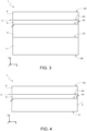
Figures 1-5 show cross-sections of a work body in subsequent manufacturing steps, according to the present manufacturing process; and -
Figure 6 shows a cross-section of the present HEMT device. -
Figure 1 shows awork body 1 comprising awafer 2 having afront surface 2A and aback surface 2B, in a Cartesian reference system XYZ comprising a first axis X, a second axis Y and a third axis Z. Thefront surface 2A and theback surface 2B of thewafer 2 respectively form a front surface and a back surface of thework body 1. - The
wafer 2 is of silicon carbide (SiC) in one of its polytypes, for example 3C, 4H, 6H, here of the polytype 4H. - The
wafer 2 is a SiC wafer of conductive type, for example having a conductivity of n-type or p-type, here of n-type. In detail, thewafer 2 has a resistivity lower than 0.1 Ω·cm, for example comprised between 0.005 Ω·cm and 0.05 Ω·cm. - For example, the
wafer 2 may have a concentration of n-type doping atoms comprised between 1.1017 atoms/cm3 and 1-1019 atoms/cm3. - In this embodiment, the
wafer 2 has a cut angle such that thefront surface 2A of thewafer 2 is tilted by a non-zero angle with respect to a C-type plane or face of the crystallographic structure of the silicon carbide. - In detail, the
front surface 2A of thewafer 2 is tilted by the cut angle with respect to the face (000-1) of the 4H-SiC, wherein the values 0, 0, 0, -1 respectively indicate the indices h, k, i, 1 of Bravais-Miller. - In practice, the
surface 2A of thewafer 2 is an off-axis face of thewafer 2, in particular having a cut angle lower than 4°. - However, the
surface 2A of thewafer 2 may have a different cut angle, for example equal to zero; that is, thesurface 2A of thewafer 2 may be parallel to the face (000-1) of the 4H-SiC. - The
wafer 2 has a thickness TW along the third axis Z comprised for example between 100 µm and 500 µm, in particular comprised between 250 µm and 350 µm. - The
wafer 2 may have a width or diameter D, parallel to the first axis X, that is high, for example comprised between 50 mm and 200 mm. - The following
Figures 2-5 show, for simplicity, only a reduced portion, along the first axis X, of thewafer 2. - In
Figure 2 , anepitaxial layer 4 of silicon carbide is grown on thefront surface 2A of thewafer 2. Theepitaxial layer 4 has asurface 4A and a thickness TE, along the third axis Z, comprised for example between 60 µm and 100 µm. Thesurface 4A of theepitaxial layer 4 thus forms a new front surface of thework body 1. - The
epitaxial layer 4 is formed by highly resistive silicon carbide, for example having a resistivity greater than 1·104 Ω·cm. - In practice, the
epitaxial layer 4 has a greater resistivity than thewafer 2. - In detail, the
epitaxial layer 4 is grown so as to have a low concentration of doping atoms. - The
epitaxial layer 4 may have a concentration of doping atoms, for example of n-type such as nitrogen atoms, lower than 5.1014 atoms/cm3, in particular comprised between 5·1011 and 5·1013 atoms/cm3. - The
epitaxial layer 4 may maintain the crystallographic orientation of thefront surface 2A of thewafer 2. Consequently, in this embodiment, thesurface 4A of theepitaxial layer 4 may maintain the same cut angle as thefront surface 2A of thewafer 2. - In practice, the crystalline structure of the
epitaxial layer 4 changes as a function of the cut angle of thefront surface 2A of thewafer 2. - For example, the fact that the
epitaxial layer 4 grows epitaxially on the off-axis face of thewafer 2 may cause a step-flow growth of theepitaxial layer 4. Theepitaxial layer 4 may thus have a terrace structure indicating said epitaxial off-axis growth. - Said terraces may be observed through superficial morphological analysis of the
epitaxial layer 4. - Then,
Figure 3 , aheterostructure 5 is grown on thesurface 4A of theepitaxial layer 4. Theheterostructure 5 has asurface 5A which forms a new front surface of thework body 1. - The
heterostructure 5 comprises compound semiconductor materials including elements of the group III-V. - In detail, the
heterostructure 5 is formed by achannel layer 6 of a first semiconductor material, for example gallium nitride (GaN) or an alloy comprising gallium nitride such as InGaN, here of intrinsic gallium nitride (GaN), extending on theepitaxial layer 4, and by abarrier layer 8 of a second semiconductor material, for example a compound based on a ternary or quaternary alloy of gallium nitride, such as AlxGa1-xN, AlInGaN, InxGa1-xN, AlxIn1-xAl, AlScN, here of intrinsic aluminum gallium nitride (AlGaN), extending on thechannel layer 6. - In detail, the
channel layer 6 extends on thesurface 4A of theepitaxial layer 4, in direct contact therewith. - The
barrier layer 8 extends on thechannel layer 6, in direct contact therewith; theheterostructure 5 therefore comprises aninterface 6A between thechannel layer 6 and thebarrier layer 8. - Subsequently,
Figure 4 , thewafer 2 is removed. For example, thewafer 2 may be removed through a thinning process such as mechanical grinding, chemical mechanical polishing (CMP) or slicing through a laser process. - To verify the complete removal of the
wafer 2, the state of removal of thewafer 2 may be controlled through an electrical measurement, for example through a mercury probe C-V measurement, or through an optical measurement. - In practice, the
epitaxial layer 4 now forms the back surface, here indicated by 11, of thework body 1. - Subsequently,
Figure 5 , asource region 13, adrain region 15, an insulation orpassivation layer 16 and agate region 17 are formed in a per se known manner and not further described herein. - The
source region 13 and thedrain region 15 are of conductive material and extend in direct electrical contact with theheterostructure 5, in particular in ohmic contact with thechannel layer 6. - In this embodiment, the
source region 13 and thedrain region 15 extend in depth into theheterostructure 5, up to theinterface 6A. However, thesource region 13 and thedrain region 15 may extend into theheterostructure 5 up to a different depth, depending on the specific application. - The
insulation layer 16 is of dielectric material, for example silicon nitride or silicon oxide and extends on thesurface 5A of theheterostructure 5. - The
gate region 17 comprises conductive material and extends through theinsulation layer 16, between thesource region 13 and thedrain region 15, in direct electrical contact with theheterostructure 5. - For example, the
gate region 17 may be formed by a single conductive layer or by a stack of conductive layers, comprising for example gold, nickel, titanium, etc., depending on the specific application. - According to an embodiment, the
gate region 17 may be formed by an insulating layer, in direct contact with theheterostructure 5, and one or more conductive layers extending on the insulating layer, so that the one or more conductive layers are not in direct electrical contact with theheterostructure 5. - According to an embodiment, the
gate region 17 may also partially extend within theheterostructure 5, depending on the specific application. - The
work body 1 is then subject to final manufacturing steps such as dicing and electrical connection, of a per se known type, thus forming a HEMT device 50 (Figure 6 ). - The
HEMT device 50 is particularly suitable for being used in RF applications, such as for example 4G and 5G base stations, including technology evolutions and variants, mobile phones, RF heat treatment devices, drying and heating devices, devices and systems for avionics, L- and S-band radar, and the like. - The
HEMT device 50 is formed in a body or die 55 having aback surface 57 and comprises an epitaxial substrate 4 (corresponding to theepitaxial layer 4 and therefore indicated by the same reference number) and theheterostructure 5 extending in direct contact on theepitaxial substrate 4. - The
epitaxial substrate 4 has a thickness along the third axis Z comprised, for example, between 60 µm and 100 µm, and forms theback surface 57 of thebody 55. - In practice, the
back surface 57 is an external surface of thebody 55, delimiting thebody 55 at the back. - The
source region 13, thedrain region 15 and thegate region 17 respectively form a source electrode S, a drain electrode D and a gate electrode G of theHEMT device 50. - The
body 55 accommodates anactive region 60, indicated by a dashed line inFigure 6 , which accommodates, in use, a conductive channel of theHEMT device 50. - In use, the fact that the
epitaxial substrate 4 has a low concentration of impurities and therefore a high resistivity, causes theHEMT device 50 to have low conductive losses through theepitaxial substrate 4, especially in radiofrequency applications. - In fact, in radiofrequency applications, the
back surface 57 of theHEMT device 50 may be used, for example, as the RF reference (ground) terminal of theHEMT device 50. In this case, the high resistivity of theepitaxial substrate 4 allows to reduce the conductive losses between thegate region 17 and theback surface 57 and thus improve the RF performances of theHEMT device 50. - Furthermore, the fact that the manufacturing of the
HEMT device 50 starts from thewafer 2, which is of conductive type, allows the use of SiC wafers having a large diameter and at the same time having a low cost, for example the diameter D of thewafer 2 may be up to 200 mm, or even greater. - The possibility of using SiC wafers having large dimension and a low cost allows the manufacturing costs of the
HEMT device 50 to be further reduced. - Finally, it is clear that modifications and variations may be made to the
HEMT device 50 and to the manufacturing process thereof described and illustrated herein without thereby departing from the scope of the present invention, as defined in the attached claims. - For example, the
channel layer 6 and thebarrier layer 8 may each be formed by a plurality of layers superimposed on each other, for example one or more layers of GaN, or GaN-based alloys, suitably doped or of intrinsic type, depending on the specific application. - For example, the
HEMT device 50 may be of normally-off or normally-on type. - For example, the
source region 13, thedrain region 15 and thegate region 17 may have shapes other than what has been shown, depending on the specific application and on the specific design requirements. - The
source region 13, thedrain region 15 and thegate region 17 may extend along the second axis Y according to different shapes and configurations, depending on the specific application, in a manner known per se and therefore not discussed in detail. For example, in a top-plan view, here not shown, thesource region 13, thedrain region 15 and thegate region 17 may have a shape of elongated strips along the second axis Y, or may have a circular shape or any other shape, regular or non-regular. - For example, the
source region 13, thedrain region 15 and thegate region 17 may each form a portion of a respective region having a more complex shape and electrically connected to other portions through specific electrical connections. - The manufacturing steps shown in
Figures 1-5 may be performed in a different order from that shown. For example, thesource region 13, thedrain region 15 and thegate region 17 may be formed before thewafer 2 is removed. Otherwise, thewafer 2 may be removed before theheterostructure 5 is grown.
Claims (15)
- A manufacturing process of a HEMT device (50) comprising, from a wafer (2) of silicon carbide having a surface (2A):forming an epitaxial layer (4) of silicon carbide on the surface (2A) of the wafer (2);forming a semiconductive heterostructure (62) on the epitaxial layer; andremoving the wafer of silicon carbide.
- The manufacturing process according to the preceding claim, removing the wafer of silicon carbide is performed after forming a semiconductive heterostructure.
- The manufacturing process according to claim 1 or 2, wherein the wafer of silicon carbide has a first resistivity and the epitaxial layer has a second resistivity greater than the first resistivity.
- The manufacturing process according to the preceding claim, wherein the first resistivity is lower than 0.1 Ω·cm.
- The manufacturing process according to claim 3 or 4, wherein the second resistivity is greater than 1·104 Ω·cm.
- The manufacturing process according to any of claims 1-5, wherein the epitaxial layer has a concentration of doping atoms lower than 5.1014 atoms/cm3, for example comprised between 5·1011 and 5·1013 atoms/cm3.
- The manufacturing process according to any of the preceding claims, wherein the surface (2A) of the wafer of silicon carbide has a non-zero cut angle with respect to a C-type plane of the wafer (2).
- The manufacturing process according to the preceding claim, wherein the cut angle is lower than 4°.
- The manufacturing process according to any of the preceding claims, wherein the epitaxial layer (4) has a thickness comprised between 60 µm and 100 µm.
- The manufacturing process according to any of the preceding claims, wherein the wafer (2) of silicon carbide is removed through a thinning process comprising mechanical grinding, chemical-mechanical polishing or laser slicing.
- A HEMT device (50) formed in a semiconductor body (55) having an external surface (57), the HEMT device comprising:a substrate (4) of silicon carbide forming the external surface of the semiconductor body; anda semiconductive heterostructure (5) extending on the substrate,wherein the substrate (4) is of epitaxial type.
- The HEMT device according to the preceding claim, wherein the substrate has a concentration of doping atoms lower than 5.1014 atoms/cm3, for example comprised between 5·1011 and 5·1013 atoms/cm3.
- The HEMT device according to claim 11 or 12, wherein the substrate (4) has a surface (4A) that is off-axis with respect to a C-type plane of the silicon carbide, the semiconductive heterostructure (5) extending in direct contact on the surface (4A) of the substrate.
- The HEMT device according to any of claims 11-13, wherein the substrate (4) has a resistivity greater than 1·104 Ω·cm.
- The HEMT device according to any of claims 11-14, wherein the substrate has a thickness comprised between 60 µm and 100 µm.
Applications Claiming Priority (1)
| Application Number | Priority Date | Filing Date | Title |
|---|---|---|---|
| IT102022000002846A IT202200002846A1 (en) | 2022-02-16 | 2022-02-16 | HEMT DEVICE HAVING LOW CONDUCTION LOSSES AND RELATED MANUFACTURING PROCEDURE |
Publications (1)
| Publication Number | Publication Date |
|---|---|
| EP4231360A1 true EP4231360A1 (en) | 2023-08-23 |
Family
ID=81392580
Family Applications (1)
| Application Number | Title | Priority Date | Filing Date |
|---|---|---|---|
| EP23156230.7A Pending EP4231360A1 (en) | 2022-02-16 | 2023-02-13 | Hemt device having low conduction losses and manufacturing process thereof |
Country Status (4)
| Country | Link |
|---|---|
| US (2) | US12520517B2 (en) |
| EP (1) | EP4231360A1 (en) |
| CN (2) | CN116613064A (en) |
| IT (1) | IT202200002846A1 (en) |
Citations (1)
| Publication number | Priority date | Publication date | Assignee | Title |
|---|---|---|---|---|
| JP5212202B2 (en) * | 2009-03-19 | 2013-06-19 | 富士通株式会社 | Method for manufacturing compound semiconductor device |
Family Cites Families (5)
| Publication number | Priority date | Publication date | Assignee | Title |
|---|---|---|---|---|
| ITMI20061809A1 (en) | 2006-09-25 | 2008-03-26 | E T C Srl | PROCESS FOR REALIZING A SILICON CARBIDE SUSTRATE FOR MICROELECTRONIC APPLICATIONS |
| JP5803786B2 (en) * | 2012-04-02 | 2015-11-04 | 住友電気工業株式会社 | Silicon carbide substrate, semiconductor device and manufacturing method thereof |
| SE1430022A1 (en) * | 2013-07-01 | 2015-01-02 | Cheap semi-insulating SiC substrates | |
| CN106981423B (en) | 2017-04-12 | 2019-08-02 | 成都海威华芯科技有限公司 | Process method of epitaxial SiC-based GaN HEMT based on Si substrate |
| US10847647B2 (en) * | 2019-03-14 | 2020-11-24 | Cree, Inc. | Power semiconductor devices having top-side metallization structures that include buried grain stop layers |
-
2022
- 2022-02-16 IT IT102022000002846A patent/IT202200002846A1/en unknown
-
2023
- 2023-02-10 US US18/167,623 patent/US12520517B2/en active Active
- 2023-02-13 EP EP23156230.7A patent/EP4231360A1/en active Pending
- 2023-02-15 CN CN202310117565.7A patent/CN116613064A/en active Pending
- 2023-02-15 CN CN202320221405.2U patent/CN220121844U/en active Active
-
2025
- 2025-12-09 US US19/413,745 patent/US20260096130A1/en active Pending
Patent Citations (1)
| Publication number | Priority date | Publication date | Assignee | Title |
|---|---|---|---|---|
| JP5212202B2 (en) * | 2009-03-19 | 2013-06-19 | 富士通株式会社 | Method for manufacturing compound semiconductor device |
Non-Patent Citations (3)
| Title |
|---|
| HOKE W ET AL: "Reaction of molecular beam epitaxial grown AlN nucleation layers with SiC substrates", JOURNAL OF VACUUM SCIENCE AND TECHNOLOGY: PART B, AVS / AIP, MELVILLE, NEW YORK, NY, US, vol. 24, no. 3, 30 May 2006 (2006-05-30), pages 1500 - 1504, XP012091520, ISSN: 1071-1023, DOI: 10.1116/1.2192539 * |
| ISHIJI KOTARO ET AL: "Characterization of Defect Structure in Epilayer Grown on On-Axis SiC by Synchrotron X-ray Topography", JOURNAL OF ELECTRONIC MATERIALS, SPRINGER US, NEW YORK, vol. 51, no. 4, 16 January 2022 (2022-01-16), pages 1541 - 1547, XP037709359, ISSN: 0361-5235, [retrieved on 20220116], DOI: 10.1007/S11664-021-09423-4 * |
| RAJENDRA DAHAL ET AL: "Fabrication of Thick Free-Standing Lightly-Doped n-Type 4H-SiC Wafers", MATERIALS SCIENCE FORUM, vol. 897, 15 May 2017 (2017-05-15), pages 379 - 382, XP055500219, DOI: 10.4028/www.scientific.net/MSF.897.379 * |
Also Published As
| Publication number | Publication date |
|---|---|
| CN220121844U (en) | 2023-12-01 |
| IT202200002846A1 (en) | 2023-08-16 |
| US20230261100A1 (en) | 2023-08-17 |
| US12520517B2 (en) | 2026-01-06 |
| US20260096130A1 (en) | 2026-04-02 |
| CN116613064A (en) | 2023-08-18 |
Similar Documents
| Publication | Publication Date | Title |
|---|---|---|
| US20250098200A1 (en) | Gallium nitride enhancement mode device | |
| JP6554530B2 (en) | Group III nitride transistor using regrowth structure | |
| US10923585B2 (en) | High electron mobility transistors having improved contact spacing and/or improved contact vias | |
| TWI520331B (en) | Thick semi-insulating or insulating epitaxial gallium nitride layer and device incorporating the same | |
| KR102626266B1 (en) | Group iii-nitride high-electron mobility transistors with buried p-type layers and process for making the same | |
| EP2428996A2 (en) | Gallium Nitride Based Semiconductor Devices and Methods of Manufacturing the Same | |
| JP2013089970A (en) | Group iii metal nitride-insulator semiconductor heterostructure field effect transistor | |
| US9136397B2 (en) | Field-effect semiconductor device | |
| WO2005119787A1 (en) | Methods of fabricating nitride-based transistors having regrown ohmic contact regions and nitride-based transistors having regrown ohmic contact regions | |
| US11961888B2 (en) | Extrinsic field termination structures for improving reliability of high-voltage, high-power active devices | |
| US20160372609A1 (en) | Schottky barrier diode | |
| WO2014025722A2 (en) | Method and system for gallium nitride electronic devices using engineered substrates | |
| US9029210B2 (en) | GaN vertical superjunction device structures and fabrication methods | |
| US8350295B1 (en) | Device structure including high-thermal-conductivity substrate | |
| US20230170408A1 (en) | Semiconductor structures and manufacturing methods thereof | |
| CN108352408B (en) | Semiconductor device, electronic component, electronic apparatus, and method for manufacturing semiconductor device | |
| US20210359118A1 (en) | Group III-Nitride High-Electron Mobility Transistors Configured with Recessed Source and/or Drain Contacts for Reduced On State Resistance and Process for Implementing the Same | |
| EP4498422A1 (en) | Semiconductor electronic device comprising an electronic component based on heterostructure and manufacturing process | |
| US20250037998A1 (en) | Manufacturing process of a semiconductor electronic device integrating different electronic components and semiconductor electronic device | |
| JP2016533028A (en) | Electronic device using group III nitride semiconductor, manufacturing method thereof, and epitaxial multilayer wafer for manufacturing the electronic device | |
| US12520517B2 (en) | HEMT device having low conduction losses and manufacturing process thereof | |
| CN114335172A (en) | Semiconductor structure | |
| CN107958931A (en) | One kind nitridation Gallium base heterojunctions field-effect transistor structure of resistance to breakdown | |
| US20250040163A1 (en) | Manufacturing process of a semiconductor electronic device integrating different electronic components and semiconductor electronic device | |
| US11552188B2 (en) | High-voltage semiconductor structure |
Legal Events
| Date | Code | Title | Description |
|---|---|---|---|
| PUAI | Public reference made under article 153(3) epc to a published international application that has entered the european phase |
Free format text: ORIGINAL CODE: 0009012 |
|
| STAA | Information on the status of an ep patent application or granted ep patent |
Free format text: STATUS: THE APPLICATION HAS BEEN PUBLISHED |
|
| AK | Designated contracting states |
Kind code of ref document: A1 Designated state(s): AL AT BE BG CH CY CZ DE DK EE ES FI FR GB GR HR HU IE IS IT LI LT LU LV MC ME MK MT NL NO PL PT RO RS SE SI SK SM TR |
|
| STAA | Information on the status of an ep patent application or granted ep patent |
Free format text: STATUS: REQUEST FOR EXAMINATION WAS MADE |
|
| 17P | Request for examination filed |
Effective date: 20240222 |
|
| RBV | Designated contracting states (corrected) |
Designated state(s): AL AT BE BG CH CY CZ DE DK EE ES FI FR GB GR HR HU IE IS IT LI LT LU LV MC ME MK MT NL NO PL PT RO RS SE SI SK SM TR |
|
| STAA | Information on the status of an ep patent application or granted ep patent |
Free format text: STATUS: EXAMINATION IS IN PROGRESS |
|
| 17Q | First examination report despatched |
Effective date: 20250725 |