EP4227987A1 - Semiconductor module - Google Patents
Semiconductor module Download PDFInfo
- Publication number
- EP4227987A1 EP4227987A1 EP20957588.5A EP20957588A EP4227987A1 EP 4227987 A1 EP4227987 A1 EP 4227987A1 EP 20957588 A EP20957588 A EP 20957588A EP 4227987 A1 EP4227987 A1 EP 4227987A1
- Authority
- EP
- European Patent Office
- Prior art keywords
- base plate
- semiconductor module
- terminal
- hole
- extension part
- Prior art date
- Legal status (The legal status is an assumption and is not a legal conclusion. Google has not performed a legal analysis and makes no representation as to the accuracy of the status listed.)
- Pending
Links
Images




Classifications
-
- H—ELECTRICITY
- H10—SEMICONDUCTOR DEVICES; ELECTRIC SOLID-STATE DEVICES NOT OTHERWISE PROVIDED FOR
- H10W—GENERIC PACKAGES, INTERCONNECTIONS, CONNECTORS OR OTHER CONSTRUCTIONAL DETAILS OF DEVICES COVERED BY CLASS H10
- H10W70/00—Package substrates; Interposers; Redistribution layers [RDL]
- H10W70/40—Leadframes
- H10W70/421—Shapes or dispositions
- H10W70/424—Cross-sectional shapes
-
- H—ELECTRICITY
- H10—SEMICONDUCTOR DEVICES; ELECTRIC SOLID-STATE DEVICES NOT OTHERWISE PROVIDED FOR
- H10W—GENERIC PACKAGES, INTERCONNECTIONS, CONNECTORS OR OTHER CONSTRUCTIONAL DETAILS OF DEVICES COVERED BY CLASS H10
- H10W70/00—Package substrates; Interposers; Redistribution layers [RDL]
- H10W70/40—Leadframes
- H10W70/421—Shapes or dispositions
-
- H—ELECTRICITY
- H10—SEMICONDUCTOR DEVICES; ELECTRIC SOLID-STATE DEVICES NOT OTHERWISE PROVIDED FOR
- H10W—GENERIC PACKAGES, INTERCONNECTIONS, CONNECTORS OR OTHER CONSTRUCTIONAL DETAILS OF DEVICES COVERED BY CLASS H10
- H10W70/00—Package substrates; Interposers; Redistribution layers [RDL]
- H10W70/40—Leadframes
- H10W70/464—Additional interconnections in combination with leadframes
- H10W70/466—Tape carriers or flat leads
-
- H—ELECTRICITY
- H10—SEMICONDUCTOR DEVICES; ELECTRIC SOLID-STATE DEVICES NOT OTHERWISE PROVIDED FOR
- H10W—GENERIC PACKAGES, INTERCONNECTIONS, CONNECTORS OR OTHER CONSTRUCTIONAL DETAILS OF DEVICES COVERED BY CLASS H10
- H10W70/00—Package substrates; Interposers; Redistribution layers [RDL]
- H10W70/40—Leadframes
- H10W70/481—Leadframes for devices being provided for in groups H10D8/00 - H10D48/00
-
- H—ELECTRICITY
- H10—SEMICONDUCTOR DEVICES; ELECTRIC SOLID-STATE DEVICES NOT OTHERWISE PROVIDED FOR
- H10W—GENERIC PACKAGES, INTERCONNECTIONS, CONNECTORS OR OTHER CONSTRUCTIONAL DETAILS OF DEVICES COVERED BY CLASS H10
- H10W90/00—Package configurations
-
- H—ELECTRICITY
- H10—SEMICONDUCTOR DEVICES; ELECTRIC SOLID-STATE DEVICES NOT OTHERWISE PROVIDED FOR
- H10W—GENERIC PACKAGES, INTERCONNECTIONS, CONNECTORS OR OTHER CONSTRUCTIONAL DETAILS OF DEVICES COVERED BY CLASS H10
- H10W90/00—Package configurations
- H10W90/811—Multiple chips on leadframes
-
- H—ELECTRICITY
- H10—SEMICONDUCTOR DEVICES; ELECTRIC SOLID-STATE DEVICES NOT OTHERWISE PROVIDED FOR
- H10W—GENERIC PACKAGES, INTERCONNECTIONS, CONNECTORS OR OTHER CONSTRUCTIONAL DETAILS OF DEVICES COVERED BY CLASS H10
- H10W72/00—Interconnections or connectors in packages
- H10W72/071—Connecting or disconnecting
- H10W72/075—Connecting or disconnecting of bond wires
- H10W72/07551—Connecting or disconnecting of bond wires characterised by changes in properties of the bond wires during the connecting
- H10W72/07554—Connecting or disconnecting of bond wires characterised by changes in properties of the bond wires during the connecting changes in dispositions
-
- H—ELECTRICITY
- H10—SEMICONDUCTOR DEVICES; ELECTRIC SOLID-STATE DEVICES NOT OTHERWISE PROVIDED FOR
- H10W—GENERIC PACKAGES, INTERCONNECTIONS, CONNECTORS OR OTHER CONSTRUCTIONAL DETAILS OF DEVICES COVERED BY CLASS H10
- H10W72/00—Interconnections or connectors in packages
- H10W72/071—Connecting or disconnecting
- H10W72/076—Connecting or disconnecting of strap connectors
-
- H—ELECTRICITY
- H10—SEMICONDUCTOR DEVICES; ELECTRIC SOLID-STATE DEVICES NOT OTHERWISE PROVIDED FOR
- H10W—GENERIC PACKAGES, INTERCONNECTIONS, CONNECTORS OR OTHER CONSTRUCTIONAL DETAILS OF DEVICES COVERED BY CLASS H10
- H10W72/00—Interconnections or connectors in packages
- H10W72/50—Bond wires
-
- H—ELECTRICITY
- H10—SEMICONDUCTOR DEVICES; ELECTRIC SOLID-STATE DEVICES NOT OTHERWISE PROVIDED FOR
- H10W—GENERIC PACKAGES, INTERCONNECTIONS, CONNECTORS OR OTHER CONSTRUCTIONAL DETAILS OF DEVICES COVERED BY CLASS H10
- H10W72/00—Interconnections or connectors in packages
- H10W72/60—Strap connectors, e.g. thick copper clips for grounding of power devices
-
- H—ELECTRICITY
- H10—SEMICONDUCTOR DEVICES; ELECTRIC SOLID-STATE DEVICES NOT OTHERWISE PROVIDED FOR
- H10W—GENERIC PACKAGES, INTERCONNECTIONS, CONNECTORS OR OTHER CONSTRUCTIONAL DETAILS OF DEVICES COVERED BY CLASS H10
- H10W72/00—Interconnections or connectors in packages
- H10W72/851—Dispositions of multiple connectors or interconnections
- H10W72/853—On the same surface
- H10W72/871—Bond wires and strap connectors
-
- H—ELECTRICITY
- H10—SEMICONDUCTOR DEVICES; ELECTRIC SOLID-STATE DEVICES NOT OTHERWISE PROVIDED FOR
- H10W—GENERIC PACKAGES, INTERCONNECTIONS, CONNECTORS OR OTHER CONSTRUCTIONAL DETAILS OF DEVICES COVERED BY CLASS H10
- H10W72/00—Interconnections or connectors in packages
- H10W72/90—Bond pads, in general
- H10W72/921—Structures or relative sizes of bond pads
- H10W72/926—Multiple bond pads having different sizes
-
- H—ELECTRICITY
- H10—SEMICONDUCTOR DEVICES; ELECTRIC SOLID-STATE DEVICES NOT OTHERWISE PROVIDED FOR
- H10W—GENERIC PACKAGES, INTERCONNECTIONS, CONNECTORS OR OTHER CONSTRUCTIONAL DETAILS OF DEVICES COVERED BY CLASS H10
- H10W74/00—Encapsulations, e.g. protective coatings
-
- H—ELECTRICITY
- H10—SEMICONDUCTOR DEVICES; ELECTRIC SOLID-STATE DEVICES NOT OTHERWISE PROVIDED FOR
- H10W—GENERIC PACKAGES, INTERCONNECTIONS, CONNECTORS OR OTHER CONSTRUCTIONAL DETAILS OF DEVICES COVERED BY CLASS H10
- H10W74/00—Encapsulations, e.g. protective coatings
- H10W74/10—Encapsulations, e.g. protective coatings characterised by their shape or disposition
- H10W74/111—Encapsulations, e.g. protective coatings characterised by their shape or disposition the semiconductor body being completely enclosed
-
- H—ELECTRICITY
- H10—SEMICONDUCTOR DEVICES; ELECTRIC SOLID-STATE DEVICES NOT OTHERWISE PROVIDED FOR
- H10W—GENERIC PACKAGES, INTERCONNECTIONS, CONNECTORS OR OTHER CONSTRUCTIONAL DETAILS OF DEVICES COVERED BY CLASS H10
- H10W74/00—Encapsulations, e.g. protective coatings
- H10W74/10—Encapsulations, e.g. protective coatings characterised by their shape or disposition
- H10W74/111—Encapsulations, e.g. protective coatings characterised by their shape or disposition the semiconductor body being completely enclosed
- H10W74/127—Encapsulations, e.g. protective coatings characterised by their shape or disposition the semiconductor body being completely enclosed characterised by arrangements for sealing or adhesion
-
- H—ELECTRICITY
- H10—SEMICONDUCTOR DEVICES; ELECTRIC SOLID-STATE DEVICES NOT OTHERWISE PROVIDED FOR
- H10W—GENERIC PACKAGES, INTERCONNECTIONS, CONNECTORS OR OTHER CONSTRUCTIONAL DETAILS OF DEVICES COVERED BY CLASS H10
- H10W90/00—Package configurations
- H10W90/701—Package configurations characterised by the relative positions of pads or connectors relative to package parts
- H10W90/751—Package configurations characterised by the relative positions of pads or connectors relative to package parts of bond wires
- H10W90/755—Package configurations characterised by the relative positions of pads or connectors relative to package parts of bond wires between a chip and a laterally-adjacent insulating package substrate, interpose or RDL
-
- H—ELECTRICITY
- H10—SEMICONDUCTOR DEVICES; ELECTRIC SOLID-STATE DEVICES NOT OTHERWISE PROVIDED FOR
- H10W—GENERIC PACKAGES, INTERCONNECTIONS, CONNECTORS OR OTHER CONSTRUCTIONAL DETAILS OF DEVICES COVERED BY CLASS H10
- H10W90/00—Package configurations
- H10W90/701—Package configurations characterised by the relative positions of pads or connectors relative to package parts
- H10W90/751—Package configurations characterised by the relative positions of pads or connectors relative to package parts of bond wires
- H10W90/756—Package configurations characterised by the relative positions of pads or connectors relative to package parts of bond wires between a chip and a stacked lead frame, conducting package substrate or heat sink
-
- H—ELECTRICITY
- H10—SEMICONDUCTOR DEVICES; ELECTRIC SOLID-STATE DEVICES NOT OTHERWISE PROVIDED FOR
- H10W—GENERIC PACKAGES, INTERCONNECTIONS, CONNECTORS OR OTHER CONSTRUCTIONAL DETAILS OF DEVICES COVERED BY CLASS H10
- H10W90/00—Package configurations
- H10W90/701—Package configurations characterised by the relative positions of pads or connectors relative to package parts
- H10W90/761—Package configurations characterised by the relative positions of pads or connectors relative to package parts of strap connectors
- H10W90/763—Package configurations characterised by the relative positions of pads or connectors relative to package parts of strap connectors between laterally-adjacent chips
-
- H—ELECTRICITY
- H10—SEMICONDUCTOR DEVICES; ELECTRIC SOLID-STATE DEVICES NOT OTHERWISE PROVIDED FOR
- H10W—GENERIC PACKAGES, INTERCONNECTIONS, CONNECTORS OR OTHER CONSTRUCTIONAL DETAILS OF DEVICES COVERED BY CLASS H10
- H10W90/00—Package configurations
- H10W90/701—Package configurations characterised by the relative positions of pads or connectors relative to package parts
- H10W90/761—Package configurations characterised by the relative positions of pads or connectors relative to package parts of strap connectors
- H10W90/766—Package configurations characterised by the relative positions of pads or connectors relative to package parts of strap connectors between a chip and a stacked lead frame, conducting package substrate or heat sink
-
- H—ELECTRICITY
- H10—SEMICONDUCTOR DEVICES; ELECTRIC SOLID-STATE DEVICES NOT OTHERWISE PROVIDED FOR
- H10W—GENERIC PACKAGES, INTERCONNECTIONS, CONNECTORS OR OTHER CONSTRUCTIONAL DETAILS OF DEVICES COVERED BY CLASS H10
- H10W90/00—Package configurations
- H10W90/701—Package configurations characterised by the relative positions of pads or connectors relative to package parts
- H10W90/761—Package configurations characterised by the relative positions of pads or connectors relative to package parts of strap connectors
- H10W90/767—Package configurations characterised by the relative positions of pads or connectors relative to package parts of strap connectors between a chip and a laterally-adjacent lead frame, conducting package substrate or heat sink
Definitions
- the present disclosure relates to a semiconductor module.
- a semiconductor module having therein an electronic component such as a semiconductor switching element is used.
- the semiconductor module is formed such that a semiconductor switching element is provided on a base plate which is a conductive member, electrode pads provided on upper surfaces of a plurality of semiconductor switching elements are connected by jumper wires or bonding wires, and then these are sealed with mold resin.
- a plurality of terminal portions such as positive and negative power supply terminals, an output terminal to a load, and a control terminal for controlling the semiconductor switching elements are arranged.
- a shunt resistor for current detection, and the like are also provided in addition to the plurality of semiconductor switching elements.
- a terminal structure exposed to outside from the mold resin of the semiconductor module disclosed is a structure in which a part of a base plate on which a semiconductor switching element is provided is led to outside so as to be directly used as a terminal portion (see, for example, Patent Document 1).
- an object of the present disclosure is to obtain a semiconductor module in which heat conduction from a terminal portion to a body portion of a base plate to which an electronic component is joined is suppressed.
- a semiconductor module includes: a base plate formed in a plate shape; a terminal member; an electronic component joined to one surface of the base plate; and mold resin sealing the base plate, the terminal member, and the electronic component.
- the base plate and the terminal member are conductive members and are arranged with an interval therebetween on the same plane.
- Each of the base plate and the terminal member has a body portion and a terminal portion exposed to outside from the mold resin.
- the base plate has a through hole at an extension part which is a part extending toward the terminal portion and connected to the terminal portion, in the body portion.
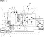
- FIG. 1 shows a circuit configuration of the entire system of an electric power steering device 200 including a semiconductor module according to embodiment 1
- FIG. 2 is a plan view showing the internal structure of a semiconductor module 100
- FIG. 3 is a side view of the semiconductor module 100
- FIG. 4 is a plan view of another semiconductor module 100 according to embodiment 1
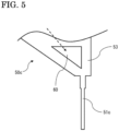
- FIG. 5 is a major part plan view of another semiconductor module 100 according to embodiment 1.
- FIG. 2 shows a state in which mold resin 70 is removed, and a two-dot dashed line indicates the outer shape of the mold resin 70.
- an outer frame 90 provided in manufacturing of the semiconductor module 100 is indicated by broken lines.
- FIG. 3 is a side view of the semiconductor module 100 as seen in the direction of arrow A shown in FIG. 2 .
- the semiconductor module 100 is used for a device that performs power conversion, and the like, and is a module having therein a plurality of semiconductor switching elements 41, 42, 44 for performing power conversion.
- the control unit 1 is composed of the control circuit 3 including a CPU 30, an inverter circuit 4 for supplying current to the windings of the motor 2, a power supply relay 5, and other electric components.
- the control unit 1 is connected to the battery 9 and the ignition switch 10, and power is supplied to the control unit 1 via the battery 9 and the ignition switch 10.
- the control unit 1 is connected to the rotation sensor 6 and the sensor 8, and electric signals outputted from these sensors are inputted to the control circuit 3 provided to the control unit 1.
- the control circuit 3 is composed of the CPU 30, a driving circuit 31, an input circuit 32, and a power supply circuit 33 connected to these circuits.
- the input circuit 32 receives output signals from the rotation sensor 6 and the sensor 8, and outputs data such as rotation angle information of the motor 2 obtained from these output signals, to the CPU 30.
- the CPU 30 calculates a current value for rotating the motor 2 from the inputted data.
- the CPU 30 outputs a control signal corresponding to a calculation result to the inverter circuit 4 via the driving circuit 31.
- the CPU 30 receives a current detection signal detected in the inverter circuit 4 via the input circuit 32, and the CPU 30 performs feedback control for the inverter circuit 4 on the basis of the current detection signal.
- a shunt resistor 43 for detecting current is connected downstream of the semiconductor switching element 42 on the low-potential side.
- the potential difference between both ends of the shunt resistor 43 is detected and converted to a current value.
- the inverter circuit 4 is provided with terminals 48 at both ends of the shunt resistor 43. Monitored signals for various points in the inverter circuit 4 are inputted to the CPU 30 via the input circuit 32.
- Driving of the semiconductor switching elements 41, 42, 44 is controlled on the basis of a signal outputted from the driving circuit 31 in accordance with a command from the CPU 30.
- the power supply relay 5 is provided upstream of the inverter circuit 4.
- the power supply relay 5 includes two semiconductor switching elements 5a, 5b connected in series.
- the power supply relay 5 has a relay function capable of supply/interruption of power to the inverter circuit 4.
- Capacitors 7 for smoothing are connected in parallel between the ground and the power supply to the inverter circuit 4.
- the semiconductor module 100 includes a base plate 50 formed in a plate shape, a terminal member 80, an electronic component joined to one surface of the base plate 50, and mold resin 70 sealing the base plate 50, the terminal member 80, and the electronic component.
- the base plate 50 and the terminal member 80 are conductive members made of the same material such as copper or a copper alloy.
- the base plate 50 and the terminal member 80 are arranged with an interval therebetween on the same plane.
- five base plates 50 and four terminal members 80 are provided.
- the electronic components in the semiconductor module 100 are semiconductor switching elements 41, 42, 44 and the shunt resistor 43.
- the semiconductor switching elements 41, 42, 44 are field effect transistors (FET).
- FET field effect transistors
- the semiconductor switching element 41 on the high-potential side is joined to one surface of a base plate 50a at a drain portion of the semiconductor switching element 41.
- the semiconductor switching element 42 on the low-potential side is joined to one surface of a base plate 50c at a drain portion of the semiconductor switching element 42.
- the semiconductor switching element 44 is joined to one surface of a base plate 50b at a drain portion of the semiconductor switching element 44.
- the shunt resistor 43 is joined so as to straddle one surface of the base plate 50d and one surface of the base plate 50e.
- the semiconductor switching elements 41, 42, 44 and the base plates 50 are connected by jumper wires 45 having a bridge shape and formed of a copper plate, for example.
- a jumper wire 45a connects a source portion of the semiconductor switching element 41, a source portion of the semiconductor switching element 44, and the base plate 50c.
- a jumper wire 45b connects a source portion of the semiconductor switching element 42 and the base plate 50d.
- the terminal portions 51a, 51b, 51e are large-current power terminals for which the current amount is large.
- the terminal portion 51a and the terminal portion 51e are located so as to be arranged on the right side of the semiconductor module 100.
- the terminal portion 51b is provided so as to extend in the upward direction of the semiconductor module 100.
- a terminal extending to outside from a side surface of the mold resin 70 on the side opposite to a side surface of the mold resin 70 from which the terminal portion 51b extends, is a control terminal.
- the direction in which the control terminal is exposed is a direction parallel to the same plane on which the base plates 50 are provided.
- the base plate 50d and the base plate 50e have a terminal portion 51d and a terminal portion 51e1 for detecting voltage between both ends of the shunt resistor 43.
- the terminal portion 51e and the terminal portion 51e1 are at the ground potential.
- the base plate 50c has a terminal portion 51c connected to the connection point between the semiconductor switching elements 41, 42, 44.
- the terminal portion 51c is a terminal for monitoring the potential at the connection point between the semiconductor switching elements 41, 42, 44.
- the wire bonding is performed using the gate portion of each semiconductor switching element 41, 42, 44 as a start point and the terminal member 80 side as a finish point. Therefore, in the wire bonding process, the bonding wire 46 can be cut without damaging each semiconductor switching element 41, 42, 44.
- a body portion 82d of a terminal member 80d and a body portion 52b of the base plate 50b are connected by the bonding wire 47.
- the terminal member 80d is a terminal for monitoring the potential of the terminal portion 51b to be outputted to the motor 2.
- the mold resin 70 seals the base plates 50, the terminal members 80, the semiconductor switching elements 41, 42, 44 and the shunt resistor 43 which are electronic components, the jumper wires 45, and the bonding wires 46, 47.
- the outer shape of the mold resin 70 is formed to be a rectangular plate shape having a plate surface parallel to the same plane on which the base plates 50 are provided.
- the outer shape of the mold resin 70 is not limited to a rectangular plate shape, and for example, may be a shape corresponding to the shape of a part where the semiconductor module 100 is mounted.
- the other surface of the base plate 50 may be exposed from the mold resin 70 so that the base plate 50 is readily cooled.
- a manufacturing method for the semiconductor module 100 includes a step of cutting out a plate-shaped conductive member to form a member in which the base plates 50 and the terminal members 80 are connected to the outer frame 90, a step of joining the semiconductor switching elements 41, 42, 44 and the shunt resistor 43 which are electronic components to the base plates 50, a step of connecting the semiconductor switching elements 41, 42, 44 and the base plates 50 by the jumper wires 45, a step of connecting the terminal members 80, and the semiconductor switching elements 41, 42, 44 and the base plate 50b, by the bonding wires 46, 47, a step of sealing the base plates 50, the terminal members 80, the semiconductor switching elements 41, 42, 44, the shunt resistor 43, the jumper wires 45, and the bonding wires 46, 47 with the mold resin 70, and a step of separating the outer frame 90 and the terminal portions 51, 81 from each other.
- the semiconductor module 100 is completed. Since the base plates 50 and the terminal members 80 respectively have the terminal portions 51, 81 exposed to outside from the side surface of the mold resin 70, it is possible to stabilize placement of the base plates 50 and the terminal members 80 in manufacturing of the semiconductor module 100, without using another fixation member such as a jig. Since placement of the base plates 50 and the terminal members 80 is stable, productivity of the semiconductor module 100 can be improved.
- the base plate 50c has the through hole 60 formed in a rectangular shape, at an extension part 53 which is a part extending toward the terminal portion 51c and connected to the terminal portion 51c, in the body portion 52c.
- the extension part 53 of the body portion 52c of the base plate 50c extends in the direction in which the terminal portion 51c extends, and is connected to the terminal portion 51c.
- the reason for providing the through hole 60 will be described.
- the terminal portion provided to the semiconductor module at the time of preheating the tip of the terminal portion in a post-process of mounting the semiconductor module to a device, there is a case where heat is transferred from the terminal portion to the base plate side where the semiconductor switching element is provided, thus deteriorating soldering performance for the terminal portion. Since the current amount in the control terminal is small, the tip part thereof is formed to be thin and also a part of the control terminal led out from the mold resin need not be as thick as the power terminal. Therefore, such a structure that the thinned control terminal extends from the base plate so as to hamper flow of heat can be adopted in terms of the layout of the semiconductor module.
- the thinned control terminal extends from the base plate, rigidity of the control terminal is reduced.
- the thinned control terminal extends from the outer frame to the base plate so as to form a cantilever shape, and thus the control terminal becomes more deflectable.
- the control terminal When the control terminal deflects, a part of the base plate where the control terminal extends is also deformed accordingly. If the base plate is deformed, a level difference arises between the base plate and another base plate provided adjacently. The outer shape of the semiconductor module is deformed due to the level difference, so that the semiconductor module becomes a defective product.
- the control terminal is provided with the extension part 53 extending toward the terminal portion 51c, so as to suppress deflection and ensure rigidity of the control terminal. Further, in order to suppress heat conduction from the terminal portion 51c to the body portion 52c of the base plate 50c, the through hole 60 formed in a rectangular shape and for reducing the sectional area of the base plate 50c is provided at the extension part 53.
- the through hole 60 is formed in an area, inside the mold resin 70, of the extension part 53 of the body portion 52c of the base plate 50c. Since the through hole 60 is provided inside the mold resin 70, the adhesion area between the base plate 50c and the mold resin 70 can be increased. Since the adhesion area between the base plate 50c and the mold resin 70 is increased, separation between the base plate 50c and the mold resin 70 can be suppressed as compared to a case of not having the through hole 60.
- the outer frame 90 to be cut in the post-process can be cut into an area between the tip part of the terminal portion 51c and the extension part 53 (area enclosed by a dotted-dashed line in FIG. 2 ), and thus the terminal portion 51c can be thinned without directly extending from the extension part 53, whereby heat conduction can be efficiently hampered.
- the long-side lines of the through hole 60 are parallel to the direction in which the terminal portion 51c and the extension part 53 of the body portion 52c of the base plate 50c extend.
- the through hole 60 is formed in a thin elongated shape along the extension part 53, whereby the widths of the through hole 60 and the extension part 53 can be reduced.
- the semiconductor module 100 can be downsized.
- the respective widths on both sides of the long-side lines of the through hole 60 in the extension part 53 of the body portion 52c of the base plate 50c is not less than the width of the tip part of the terminal portion 51c.
- the respective widths on both sides of the long-side lines of the through hole 60 in the extension part 53 of the body portion 52c of the base plate 50c are equal to each other. With this structure, heat conduction in the extension part 53 on both sides of the long-side lines of the through hole 60 is uniformed, whereby heat conduction from the terminal portion 51c to the body portion 52c of the base plate 50c can be efficiently suppressed.
- the through hole 60 formed at the extension part 53 of the base plate 50c extends in not only the extension part 53 but also a part where the semiconductor switching element 42 is not joined in the body portion 52c of the base plate 50c, as shown in FIG. 2 .
- Providing the through hole 60 so as to thus extend can further suppress heat conduction from the terminal portion 51c to the body portion 52c of the base plate 50c.
- the part where the through hole 60 is provided is not limited thereto, and as shown in FIG. 4 , the through hole 60 may be provided only at the extension part 53 of the base plate 50c.
- the extension part 53 of the base plate 50c extends in the direction in which the terminal portion 51c extends, and is connected to the terminal portion 51c, as shown in FIG. 2 .
- formation of the extension part 53 is not limited thereto.
- the extension part 53 may extend in a direction (direction of a broken-line arrow shown in FIG. 5 ) different from the direction in which the terminal portion 51c extends, and may be connected to the terminal portion 51c.
- the shape of the through hole 60 is not limited to a rectangular shape. In such a case where the extension part 53 extends in a direction different from the direction in which the terminal portion 51c extends, the shape of the through hole 60 may be a triangular shape as shown in FIG.
- extension part 53 and the through hole 60 are provided at a part connected to the control terminal in the body portion 52.
- the extension part 53 and the through hole 60 may be provided at a part connected to the power terminal in the body portion 52.
- the base plate 50c to which the semiconductor switching element 42 is joined has the body portion 52c and the terminal portion 51c exposed to outside from the mold resin 70, and the base plate 50c has the through hole 60 at the extension part 53 which is a part extending toward the terminal portion 51c and connected to the terminal portion 51c, in the body portion 52c.
- the sectional area of the base plate 50c is reduced at the extension part 53, whereby heat conduction from the terminal portion 51c to the body portion 52c of the base plate 50c can be suppressed.
- the adhesion area between the base plate 50c and the mold resin 70 can be increased, whereby separation between the base plate 50c and the mold resin 70 can be suppressed as compared to a case of not having the through hole 60.
- the width of the extension part 53 can be reduced, whereby the semiconductor module 100 can be downsized.
- the through hole 60 is formed in a thin elongated shape along the extension part 53, whereby the widths of the through hole 60 and the extension part 53 can be reduced.
- the semiconductor module 100 can be downsized since the widths of the through hole 60 and the extension part 53 are reduced.
- FIG. 6 is a plan view of the semiconductor module 100 according to embodiment 2
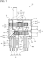
- FIG. 7 is a plan view of another semiconductor module 100 according to embodiment 2.
- FIG. 6 shows a state in which the mold resin 70 is removed, and a two-dot dashed line indicates the outer shape of the mold resin 70.
- location of the through hole 60 is different from that in embodiment 1.
- the through hole 60 is formed in an area, exposed from the mold resin 70, of the extension part 53 of the body portion 52c of the base plate 50c.
- the extension part 53 of the body portion 52c of the base plate 50c extends in the direction in which the terminal portion 51c extends, and is connected to the terminal portion 51c. Since the through hole 60 is located so as to be exposed from the mold resin 70, the part where heat conduction from the terminal portion 51c to the body portion 52c of the base plate 50c is suppressed and heat is readily generated can be located away from the semiconductor switching elements 41, 42, 44 and the shunt resistor 43.
- the through hole 60 is located only in an area, exposed from the mold resin 70, of the extension part 53 of the base plate 50c.
- location of the through hole 60 is not limited thereto.
- a part of the through hole 60 may be additionally provided also inside the mold resin 70, as shown in FIG. 7 .
- Providing the through hole 60 inside the mold resin 70 can suppress separation between the base plate 50c and the mold resin 70.
- the width of the through hole 60 provided inside the mold resin 70 is reduced.
- parts of the through hole 60 provided both inside and outside the mold resin 70 are integrated as one through hole 60.
- the through holes 60 may be provided separately both inside and outside the mold resin 70.
- the through hole 60 is formed in an area, exposed from the mold resin 70, of the extension part 53 of the body portion 52c of the base plate 50c.
- the part where heat conduction from the terminal portion 51c to the body portion 52c of the base plate 50c is suppressed and heat is readily generated can be located away from the semiconductor switching elements 41, 42, 44 and the shunt resistor 43, whereby hampering of heat dissipation from the semiconductor switching elements 41, 42, 44 and the shunt resistor 43 which are heat generating bodies can be suppressed.
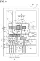
- FIG. 8 is a plan view of the semiconductor module 100 according to embodiment 3, and FIG. 9 is a major part plan view of the semiconductor module 100.
- FIG. 8 shows a state in which the mold resin 70 is removed, and a two-dot dashed line indicates the outer shape of the mold resin 70.
- location of the through hole 60 is different from that in embodiment 1.
- the extension part 53 of the body portion 52c of the base plate 50c extends in the direction in which the terminal portion 51c extends, and is connected to the terminal portion 51c.
- the long-side lines of the through hole 60 formed in a rectangular shape are parallel to the direction in which the terminal portion 51c and the extension part 53 of the body portion 52c of the base plate 50c extend.
- the respective widths on both sides of the long-side lines of the through hole 60 in the extension part 53 of the body portion 52c of the base plate 50c are different from each other, and the sum of the respective widths on both sides of the long-side lines of the through hole 60 is not less than the width of the tip part of the terminal portion 51c.
- FIG. 9 is an enlarged view of the extension part 53 and the terminal portion 51c. In FIG.
- the respective widths on both sides of the long-side lines of the through hole 60 are defined as D1 and D2.
- the width of the tip part of the terminal portion 51c is defined as D3.
- the through hole 60 is located at the extension part 53 such that the relationship of these widths satisfies (D1 + D2) ⁇ D3.
- the extension part 53 whose width is locally narrowed can be provided, whereby it is possible to provide a part where heat conduction from the terminal portion 51c to the body portion 52c of the base plate 50c is locally suppressed.
- the width D1 of the extension part 53 at a position near the semiconductor switching element 42 is greater than the width D2 of the extension part 53 at a position away from the semiconductor switching element 42.
- the respective widths on both sides of the long-side lines of the through hole 60 in the extension part 53 of the base plate 50c are different from each other, and the sum of the respective widths on both sides of the long-side lines of the through hole 60 is not less than the width of the tip part of the terminal portion 51c.
- current flowing to the tip part of the terminal portion 51c is not hampered by the extension part 53 on both sides of the long-side lines of the through hole 60, whereby heat generation in the extension part 53 due to the current can be suppressed.
Landscapes
- Structures Or Materials For Encapsulating Or Coating Semiconductor Devices Or Solid State Devices (AREA)
- Physics & Mathematics (AREA)
- Geometry (AREA)
- Inverter Devices (AREA)
Abstract
Description
- The present disclosure relates to a semiconductor module.
- For a device that performs power conversion, and the like, a semiconductor module having therein an electronic component such as a semiconductor switching element is used. The semiconductor module is formed such that a semiconductor switching element is provided on a base plate which is a conductive member, electrode pads provided on upper surfaces of a plurality of semiconductor switching elements are connected by jumper wires or bonding wires, and then these are sealed with mold resin. On an outer peripheral side surface of the mold resin, a plurality of terminal portions such as positive and negative power supply terminals, an output terminal to a load, and a control terminal for controlling the semiconductor switching elements are arranged. Inside the semiconductor module, a shunt resistor for current detection, and the like, are also provided in addition to the plurality of semiconductor switching elements.
- As a terminal structure exposed to outside from the mold resin of the semiconductor module, disclosed is a structure in which a part of a base plate on which a semiconductor switching element is provided is led to outside so as to be directly used as a terminal portion (see, for example, Patent Document 1).
- Patent Document 1:
Japanese Laid-Open Patent Publication No. 2003-324176 - In the terminal structure of the semiconductor module in Patent Document 1, at the time of preheating the tip of the terminal portion in a post-process of mounting the semiconductor module to a device, heat is transferred from the terminal portion to the base plate side where the semiconductor switching element is provided, thus causing a problem that soldering performance for the terminal portion is deteriorated.
- Accordingly, an object of the present disclosure is to obtain a semiconductor module in which heat conduction from a terminal portion to a body portion of a base plate to which an electronic component is joined is suppressed.
- A semiconductor module according to the present disclosure includes: a base plate formed in a plate shape; a terminal member; an electronic component joined to one surface of the base plate; and mold resin sealing the base plate, the terminal member, and the electronic component. The base plate and the terminal member are conductive members and are arranged with an interval therebetween on the same plane. Each of the base plate and the terminal member has a body portion and a terminal portion exposed to outside from the mold resin. The base plate has a through hole at an extension part which is a part extending toward the terminal portion and connected to the terminal portion, in the body portion.
- In the semiconductor module according to the present disclosure, the base plate to which the electronic component is joined has the body portion and the terminal portion exposed to outside from the mold resin, and the base plate has the through hole at the extension part which is the part extending toward the terminal portion and connected to the terminal portion, in the body portion. Thus, the sectional area of the base plate is reduced at the extension part, whereby the semiconductor module in which heat conduction from the terminal portion to the body portion of the base plate is suppressed can be obtained.
-
- [
FIG. 1] FIG. 1 shows a circuit configuration of a device including a semiconductor module according to embodiment 1. - [
FIG. 2] FIG. 2 is a plan view of the semiconductor module according to embodiment 1. - [
FIG. 3] FIG. 3 is a side view of the semiconductor module according to embodiment 1. - [
FIG. 4] FIG. 4 is a plan view of another semiconductor module according to embodiment 1. - [
FIG. 5] FIG. 5 is a major part plan view of another semiconductor module according to embodiment 1. - [
FIG. 6] FIG. 6 is a plan view of a semiconductor module according toembodiment 2. - [
FIG. 7] FIG. 7 is a plan view of another semiconductor module according toembodiment 2. - [
FIG. 8] FIG. 8 is a plan view of a semiconductor module according toembodiment 3. - [
FIG. 9] FIG. 9 is a major part plan view of the semiconductor module according toembodiment 3. - Hereinafter, a semiconductor module according to embodiments of the present disclosure will be described with reference to the drawings. In the drawings, the same or corresponding members and parts are denoted by the same reference characters, to give description.
-
FIG. 1 shows a circuit configuration of the entire system of an electricpower steering device 200 including a semiconductor module according to embodiment 1,FIG. 2 is a plan view showing the internal structure of asemiconductor module 100,FIG. 3 is a side view of thesemiconductor module 100,FIG. 4 is a plan view of anothersemiconductor module 100 according to embodiment 1, andFIG. 5 is a major part plan view of anothersemiconductor module 100 according to embodiment 1.FIG. 2 shows a state in whichmold resin 70 is removed, and a two-dot dashed line indicates the outer shape of themold resin 70. InFIG. 2 andFIG. 4 , anouter frame 90 provided in manufacturing of thesemiconductor module 100 is indicated by broken lines.FIG. 3 is a side view of thesemiconductor module 100 as seen in the direction of arrow A shown inFIG. 2 . Thesemiconductor module 100 is used for a device that performs power conversion, and the like, and is a module having therein a plurality ofsemiconductor switching elements - As an example of the device including the semiconductor module, the electric
power steering device 200 will be described. The electricpower steering device 200 is a device that converts power supplied from a battery 9 and outputs the converted power to amotor 2. As shown inFIG. 1 , the electricpower steering device 200 is composed of a control unit 1, themotor 2, the battery 9, anignition switch 10, and sensors such as arotation sensor 6. Themotor 2 is a brushless motor having windings for three phases (U phase, V phase, W phase). Therotation sensor 6 is provided near themotor 2, to detect the rotation angle of themotor 2, and outputs the detected rotation angle to acontrol circuit 3 provided to the control unit 1. Asensor 8 includes a torque sensor for detecting a steering wheel operation force, a vehicle speed sensor, and the like, and an electric signal corresponding to a physical quantity detected by each sensor is outputted to thecontrol circuit 3. - The control unit 1 is composed of the
control circuit 3 including aCPU 30, an inverter circuit 4 for supplying current to the windings of themotor 2, apower supply relay 5, and other electric components. The control unit 1 is connected to the battery 9 and theignition switch 10, and power is supplied to the control unit 1 via the battery 9 and theignition switch 10. The control unit 1 is connected to therotation sensor 6 and thesensor 8, and electric signals outputted from these sensors are inputted to thecontrol circuit 3 provided to the control unit 1. - The
control circuit 3 is composed of theCPU 30, adriving circuit 31, aninput circuit 32, and apower supply circuit 33 connected to these circuits. Theinput circuit 32 receives output signals from therotation sensor 6 and thesensor 8, and outputs data such as rotation angle information of themotor 2 obtained from these output signals, to theCPU 30. TheCPU 30 calculates a current value for rotating themotor 2 from the inputted data. TheCPU 30 outputs a control signal corresponding to a calculation result to the inverter circuit 4 via thedriving circuit 31. In addition, theCPU 30 receives a current detection signal detected in the inverter circuit 4 via theinput circuit 32, and theCPU 30 performs feedback control for the inverter circuit 4 on the basis of the current detection signal. - The inverter circuit 4 is formed by bridge circuits respectively corresponding to the windings for three phases, i.e., U phase, V phase, and W phase of the
motor 2. All the bridge circuits corresponding to the respective phases are the same circuit, and therefore abridge circuit 4a for one phase (U phase) will be described. Thebridge circuit 4a includes threesemiconductor switching elements semiconductor switching element 41 on the high-potential side and thesemiconductor switching element 42 on the low potential side are connected in series to each other. One side of thesemiconductor switching element 44 is connected to an intermediate connection part between thesemiconductor switching element 41 and thesemiconductor switching element 42, and the other side of thesemiconductor switching element 44 is connected to the coil for U phase of themotor 2. Thesemiconductor switching element 44 has a relay function capable of connection/interruption between the coil for U phase and the inverter circuit 4. - A
shunt resistor 43 for detecting current is connected downstream of thesemiconductor switching element 42 on the low-potential side. The potential difference between both ends of theshunt resistor 43 is detected and converted to a current value. For detecting the potential difference between both ends of theshunt resistor 43, the inverter circuit 4 is provided withterminals 48 at both ends of theshunt resistor 43. Monitored signals for various points in the inverter circuit 4 are inputted to theCPU 30 via theinput circuit 32. Driving of thesemiconductor switching elements circuit 31 in accordance with a command from theCPU 30. - The
power supply relay 5 is provided upstream of the inverter circuit 4. Thepower supply relay 5 includes twosemiconductor switching elements power supply relay 5 has a relay function capable of supply/interruption of power to the inverter circuit 4.Capacitors 7 for smoothing are connected in parallel between the ground and the power supply to the inverter circuit 4. - Various types are conceivable for implementing the control unit 1 using a semiconductor module having therein a plurality of semiconductor switching elements. Examples include a semiconductor module having therein the bridge circuits forming the inverter circuit 4, a semiconductor module having therein the
power supply relay 5, and a semiconductor module having therein a circuit in which some of the shunt resistors and the semiconductor switching elements are omitted. - A case where the
bridge circuit 4a for one phase is formed as thesemiconductor module 100 will be described. As shown inFIG. 2 , thesemiconductor module 100 includes abase plate 50 formed in a plate shape, aterminal member 80, an electronic component joined to one surface of thebase plate 50, andmold resin 70 sealing thebase plate 50, theterminal member 80, and the electronic component. Thebase plate 50 and theterminal member 80 are conductive members made of the same material such as copper or a copper alloy. Thebase plate 50 and theterminal member 80 are arranged with an interval therebetween on the same plane. Here, fivebase plates 50 and fourterminal members 80 are provided. The electronic components in thesemiconductor module 100 aresemiconductor switching elements shunt resistor 43. Here, thesemiconductor switching elements base plates 50 are not limited thereto. - The
semiconductor switching element 41 on the high-potential side is joined to one surface of abase plate 50a at a drain portion of thesemiconductor switching element 41. Thesemiconductor switching element 42 on the low-potential side is joined to one surface of abase plate 50c at a drain portion of thesemiconductor switching element 42. Thesemiconductor switching element 44 is joined to one surface of abase plate 50b at a drain portion of thesemiconductor switching element 44. Theshunt resistor 43 is joined so as to straddle one surface of thebase plate 50d and one surface of thebase plate 50e. Thesemiconductor switching elements base plates 50 are connected byjumper wires 45 having a bridge shape and formed of a copper plate, for example. Ajumper wire 45a connects a source portion of thesemiconductor switching element 41, a source portion of thesemiconductor switching element 44, and thebase plate 50c. Ajumper wire 45b connects a source portion of thesemiconductor switching element 42 and thebase plate 50d. - Each of the
base plates 50 has abody portion 52 to which the electronic component is joined, and aterminal portion 51 exposed to outside from a side surface of themold resin 70. The direction in which theterminal portion 51 is exposed is a direction parallel to the same plane on which thebase plates 50 are provided. Theterminal portion 51 extends from the side surface of themold resin 70. Aterminal portion 51a of thebase plate 50a is connected to the battery 9 which is the power supply. Aterminal portion 51e of thebase plate 50e is connected to the ground. Aterminal portion 51b of thebase plate 50b is connected to U phase of themotor 2 which is a load, and converted power is outputted from theterminal portion 51b to U phase of themotor 2. Theterminal portions FIG. 2 , theterminal portion 51a and theterminal portion 51e are located so as to be arranged on the right side of thesemiconductor module 100. InFIG. 2 , theterminal portion 51b is provided so as to extend in the upward direction of thesemiconductor module 100. - A terminal extending to outside from a side surface of the
mold resin 70 on the side opposite to a side surface of themold resin 70 from which theterminal portion 51b extends, is a control terminal. The direction in which the control terminal is exposed is a direction parallel to the same plane on which thebase plates 50 are provided. Thebase plate 50d and thebase plate 50e have aterminal portion 51d and a terminal portion 51e1 for detecting voltage between both ends of theshunt resistor 43. Theterminal portion 51e and the terminal portion 51e1 are at the ground potential. Thebase plate 50c has aterminal portion 51c connected to the connection point between thesemiconductor switching elements terminal portion 51c is a terminal for monitoring the potential at the connection point between thesemiconductor switching elements - Each of the
terminal members 80 formed in a plate shape has abody portion 82 to which abonding wire 46 or abonding wire 47 is connected, and aterminal portion 81 exposed to outside from the side surface of themold resin 70. Theterminal member 80 is a terminal for which the current amount is comparatively small and which is used for control of thesemiconductor module 100. InFIG. 2 , theterminal members 80 are located so as to be arranged on the lower side of thesemiconductor module 100.Terminal members semiconductor switching elements terminal members wires 46 provided through a wire bonding process. - The wire bonding is performed using the gate portion of each
semiconductor switching element terminal member 80 side as a finish point. Therefore, in the wire bonding process, thebonding wire 46 can be cut without damaging eachsemiconductor switching element body portion 82d of aterminal member 80d and abody portion 52b of thebase plate 50b are connected by thebonding wire 47. Theterminal member 80d is a terminal for monitoring the potential of theterminal portion 51b to be outputted to themotor 2. - The
mold resin 70 seals thebase plates 50, theterminal members 80, thesemiconductor switching elements shunt resistor 43 which are electronic components, thejumper wires 45, and thebonding wires mold resin 70 is formed to be a rectangular plate shape having a plate surface parallel to the same plane on which thebase plates 50 are provided. The outer shape of themold resin 70 is not limited to a rectangular plate shape, and for example, may be a shape corresponding to the shape of a part where thesemiconductor module 100 is mounted. The other surface of thebase plate 50 may be exposed from themold resin 70 so that thebase plate 50 is readily cooled. - Manufacturing of the
semiconductor module 100 is performed in a state in which thebase plates 50 and theterminal members 80 are connected to theouter frame 90. A manufacturing method for thesemiconductor module 100 includes a step of cutting out a plate-shaped conductive member to form a member in which thebase plates 50 and theterminal members 80 are connected to theouter frame 90, a step of joining thesemiconductor switching elements shunt resistor 43 which are electronic components to thebase plates 50, a step of connecting thesemiconductor switching elements base plates 50 by thejumper wires 45, a step of connecting theterminal members 80, and thesemiconductor switching elements base plate 50b, by thebonding wires base plates 50, theterminal members 80, thesemiconductor switching elements shunt resistor 43, thejumper wires 45, and thebonding wires mold resin 70, and a step of separating theouter frame 90 and theterminal portions - When the
outer frame 90 and theterminal portions semiconductor module 100 is completed. Since thebase plates 50 and theterminal members 80 respectively have theterminal portions mold resin 70, it is possible to stabilize placement of thebase plates 50 and theterminal members 80 in manufacturing of thesemiconductor module 100, without using another fixation member such as a jig. Since placement of thebase plates 50 and theterminal members 80 is stable, productivity of thesemiconductor module 100 can be improved. - A through
hole 60 which is a major part of the present disclosure will be described. Thebase plate 50c has the throughhole 60 formed in a rectangular shape, at anextension part 53 which is a part extending toward theterminal portion 51c and connected to theterminal portion 51c, in thebody portion 52c. Theextension part 53 of thebody portion 52c of thebase plate 50c extends in the direction in which theterminal portion 51c extends, and is connected to theterminal portion 51c. - The reason for providing the through
hole 60 will be described. Regarding the terminal portion provided to the semiconductor module, at the time of preheating the tip of the terminal portion in a post-process of mounting the semiconductor module to a device, there is a case where heat is transferred from the terminal portion to the base plate side where the semiconductor switching element is provided, thus deteriorating soldering performance for the terminal portion. Since the current amount in the control terminal is small, the tip part thereof is formed to be thin and also a part of the control terminal led out from the mold resin need not be as thick as the power terminal. Therefore, such a structure that the thinned control terminal extends from the base plate so as to hamper flow of heat can be adopted in terms of the layout of the semiconductor module. However, if the thinned control terminal extends from the base plate, rigidity of the control terminal is reduced. In addition, the thinned control terminal extends from the outer frame to the base plate so as to form a cantilever shape, and thus the control terminal becomes more deflectable. - When the control terminal deflects, a part of the base plate where the control terminal extends is also deformed accordingly. If the base plate is deformed, a level difference arises between the base plate and another base plate provided adjacently. The outer shape of the semiconductor module is deformed due to the level difference, so that the semiconductor module becomes a defective product. Considering this, the control terminal is provided with the
extension part 53 extending toward theterminal portion 51c, so as to suppress deflection and ensure rigidity of the control terminal. Further, in order to suppress heat conduction from theterminal portion 51c to thebody portion 52c of thebase plate 50c, the throughhole 60 formed in a rectangular shape and for reducing the sectional area of thebase plate 50c is provided at theextension part 53. - The through
hole 60 is formed in an area, inside themold resin 70, of theextension part 53 of thebody portion 52c of thebase plate 50c. Since the throughhole 60 is provided inside themold resin 70, the adhesion area between thebase plate 50c and themold resin 70 can be increased. Since the adhesion area between thebase plate 50c and themold resin 70 is increased, separation between thebase plate 50c and themold resin 70 can be suppressed as compared to a case of not having the throughhole 60. In addition, theouter frame 90 to be cut in the post-process can be cut into an area between the tip part of theterminal portion 51c and the extension part 53 (area enclosed by a dotted-dashed line inFIG. 2 ), and thus theterminal portion 51c can be thinned without directly extending from theextension part 53, whereby heat conduction can be efficiently hampered. - The long-side lines of the through
hole 60 are parallel to the direction in which theterminal portion 51c and theextension part 53 of thebody portion 52c of thebase plate 50c extend. With this structure, the throughhole 60 is formed in a thin elongated shape along theextension part 53, whereby the widths of the throughhole 60 and theextension part 53 can be reduced. In addition, since the widths of the throughhole 60 and theextension part 53 are reduced, thesemiconductor module 100 can be downsized. - The respective widths on both sides of the long-side lines of the through
hole 60 in theextension part 53 of thebody portion 52c of thebase plate 50c is not less than the width of the tip part of theterminal portion 51c. With this structure, since the respective widths of theextension part 53 on both sides of the long-side lines of the throughhole 60 are ensured to be not less than the width of the tip part of theterminal portion 51c, current flowing to the tip part of theterminal portion 51c is not hampered by theextension part 53 on both sides of the long-side lines of the throughhole 60. - The respective widths on both sides of the long-side lines of the through
hole 60 in theextension part 53 of thebody portion 52c of thebase plate 50c are equal to each other. With this structure, heat conduction in theextension part 53 on both sides of the long-side lines of the throughhole 60 is uniformed, whereby heat conduction from theterminal portion 51c to thebody portion 52c of thebase plate 50c can be efficiently suppressed. - In the present embodiment, the through
hole 60 formed at theextension part 53 of thebase plate 50c extends in not only theextension part 53 but also a part where thesemiconductor switching element 42 is not joined in thebody portion 52c of thebase plate 50c, as shown inFIG. 2 . Providing the throughhole 60 so as to thus extend can further suppress heat conduction from theterminal portion 51c to thebody portion 52c of thebase plate 50c. The part where the throughhole 60 is provided is not limited thereto, and as shown inFIG. 4 , the throughhole 60 may be provided only at theextension part 53 of thebase plate 50c. - In the present embodiment, the
extension part 53 of thebase plate 50c extends in the direction in which theterminal portion 51c extends, and is connected to theterminal portion 51c, as shown inFIG. 2 . However, formation of theextension part 53 is not limited thereto. As shown inFIG. 5 , theextension part 53 may extend in a direction (direction of a broken-line arrow shown inFIG. 5 ) different from the direction in which theterminal portion 51c extends, and may be connected to theterminal portion 51c. In addition, the shape of the throughhole 60 is not limited to a rectangular shape. In such a case where theextension part 53 extends in a direction different from the direction in which theterminal portion 51c extends, the shape of the throughhole 60 may be a triangular shape as shown inFIG. 5 , a trapezoidal shape, or the like. In the present embodiment, the example in which theextension part 53 and the throughhole 60 are provided at a part connected to the control terminal in thebody portion 52, has been shown. However, without limitation thereto, theextension part 53 and the throughhole 60 may be provided at a part connected to the power terminal in thebody portion 52. - As described above, in the
semiconductor module 100 according to embodiment 1, thebase plate 50c to which thesemiconductor switching element 42 is joined has thebody portion 52c and theterminal portion 51c exposed to outside from themold resin 70, and thebase plate 50c has the throughhole 60 at theextension part 53 which is a part extending toward theterminal portion 51c and connected to theterminal portion 51c, in thebody portion 52c. Thus, the sectional area of thebase plate 50c is reduced at theextension part 53, whereby heat conduction from theterminal portion 51c to thebody portion 52c of thebase plate 50c can be suppressed. In the case where the throughhole 60 is formed in an area, inside themold resin 70, of theextension part 53 of thebody portion 52c of thebase plate 50c, the adhesion area between thebase plate 50c and themold resin 70 can be increased, whereby separation between thebase plate 50c and themold resin 70 can be suppressed as compared to a case of not having the throughhole 60. - In the case where the
extension part 53 of thebody portion 52c of thebase plate 50c extends in the direction in which theterminal portion 51c extends, and is connected to theterminal portion 51c, the width of theextension part 53 can be reduced, whereby thesemiconductor module 100 can be downsized. In the case where the long-side lines of the throughhole 60 formed in a rectangular shape are parallel to the direction in which theterminal portion 51c and theextension part 53 of thebase plate 50c extend, the throughhole 60 is formed in a thin elongated shape along theextension part 53, whereby the widths of the throughhole 60 and theextension part 53 can be reduced. In addition, since the widths of the throughhole 60 and theextension part 53 are reduced, thesemiconductor module 100 can be downsized. - In the case where the respective widths on both sides of the long-side lines of the through
hole 60 in theextension part 53 of thebase plate 50c are not less than the width of the tip part of theterminal portion 51c, current flowing to the tip part of theterminal portion 51c is not hampered by theextension part 53 on both sides of the long-side lines of the throughhole 60, whereby heat generation in theextension part 53 due to the current can be suppressed. In the case where the respective widths on both sides of the long-side lines of the throughhole 60 in theextension part 53 of thebase plate 50c are equal to each other, heat conduction in theextension part 53 on both sides of the long-side lines of the throughhole 60 is uniformed, whereby heat conduction from theterminal portion 51c to thebody portion 52c of thebase plate 50c can be efficiently suppressed. - A
semiconductor module 100 according toembodiment 2 will be described.FIG. 6 is a plan view of thesemiconductor module 100 according toembodiment 2, andFIG. 7 is a plan view of anothersemiconductor module 100 according toembodiment 2.FIG. 6 shows a state in which themold resin 70 is removed, and a two-dot dashed line indicates the outer shape of themold resin 70. In thesemiconductor module 100 according toembodiment 2, location of the throughhole 60 is different from that in embodiment 1. - The through
hole 60 is formed in an area, exposed from themold resin 70, of theextension part 53 of thebody portion 52c of thebase plate 50c. Theextension part 53 of thebody portion 52c of thebase plate 50c extends in the direction in which theterminal portion 51c extends, and is connected to theterminal portion 51c. Since the throughhole 60 is located so as to be exposed from themold resin 70, the part where heat conduction from theterminal portion 51c to thebody portion 52c of thebase plate 50c is suppressed and heat is readily generated can be located away from thesemiconductor switching elements shunt resistor 43. Since the part where heat is readily generated can be located away from thesemiconductor switching elements shunt resistor 43, hampering of heat dissipation from thesemiconductor switching elements shunt resistor 43 which are heat generating bodies can be suppressed. - In the present embodiment, the through
hole 60 is located only in an area, exposed from themold resin 70, of theextension part 53 of thebase plate 50c. Therefore, thesemiconductor switching element 42 joined to thebase plate 50c can be located on the center side of thesemiconductor module 100. Since thesemiconductor switching element 42 is located on the center side of thesemiconductor module 100, heat dissipation from thesemiconductor switching element 42 is improved. In addition, ease of layout of the electronic components on thesemiconductor module 100 can be improved. In addition, thesemiconductor module 100 can be downsized. - In the present embodiment, the through
hole 60 is located only in an area, exposed from themold resin 70, of theextension part 53 of thebase plate 50c. However, location of the throughhole 60 is not limited thereto. A part of the throughhole 60 may be additionally provided also inside themold resin 70, as shown inFIG. 7 . Providing the throughhole 60 inside themold resin 70 can suppress separation between thebase plate 50c and themold resin 70. Here, for suppressing heat generation of theextension part 53 on both sides of the throughhole 60, the width of the throughhole 60 provided inside themold resin 70 is reduced. InFIG. 7 , parts of the throughhole 60 provided both inside and outside themold resin 70 are integrated as one throughhole 60. However, the throughholes 60 may be provided separately both inside and outside themold resin 70. - As described above, in the
semiconductor module 100 according toembodiment 2, the throughhole 60 is formed in an area, exposed from themold resin 70, of theextension part 53 of thebody portion 52c of thebase plate 50c. Thus, the part where heat conduction from theterminal portion 51c to thebody portion 52c of thebase plate 50c is suppressed and heat is readily generated can be located away from thesemiconductor switching elements shunt resistor 43, whereby hampering of heat dissipation from thesemiconductor switching elements shunt resistor 43 which are heat generating bodies can be suppressed. - A
semiconductor module 100 according toembodiment 3 will be described.FIG. 8 is a plan view of thesemiconductor module 100 according toembodiment 3, andFIG. 9 is a major part plan view of thesemiconductor module 100.FIG. 8 shows a state in which themold resin 70 is removed, and a two-dot dashed line indicates the outer shape of themold resin 70. In thesemiconductor module 100 according toembodiment 3, location of the throughhole 60 is different from that in embodiment 1. - The
extension part 53 of thebody portion 52c of thebase plate 50c extends in the direction in which theterminal portion 51c extends, and is connected to theterminal portion 51c. The long-side lines of the throughhole 60 formed in a rectangular shape are parallel to the direction in which theterminal portion 51c and theextension part 53 of thebody portion 52c of thebase plate 50c extend. The respective widths on both sides of the long-side lines of the throughhole 60 in theextension part 53 of thebody portion 52c of thebase plate 50c are different from each other, and the sum of the respective widths on both sides of the long-side lines of the throughhole 60 is not less than the width of the tip part of theterminal portion 51c.FIG. 9 is an enlarged view of theextension part 53 and theterminal portion 51c. InFIG. 9 , the respective widths on both sides of the long-side lines of the throughhole 60 are defined as D1 and D2. The width of the tip part of theterminal portion 51c is defined as D3. The throughhole 60 is located at theextension part 53 such that the relationship of these widths satisfies (D1 + D2) ≥ D3. With this structure, since the sum of the respective widths of theextension part 53 on both sides of the long-side lines of the throughhole 60 is ensured to be not less than the width of the tip part of theterminal portion 51c, current flowing to the tip part of theterminal portion 51c is not hampered by theextension part 53 on both sides of the long-side lines of the throughhole 60. - Since the respective widths of the
extension part 53 on both sides of the long-side lines of the throughhole 60 are different from each other, theextension part 53 whose width is locally narrowed can be provided, whereby it is possible to provide a part where heat conduction from theterminal portion 51c to thebody portion 52c of thebase plate 50c is locally suppressed. In addition, the width D1 of theextension part 53 at a position near thesemiconductor switching element 42 is greater than the width D2 of theextension part 53 at a position away from thesemiconductor switching element 42. Thus, the part where heat conduction from theterminal portion 51c to thebody portion 52c of thebase plate 50c is suppressed and heat is readily generated can be located away from thesemiconductor switching element 42, whereby hampering of heat dissipation from thesemiconductor switching element 42 which is a heat generating body can be suppressed. - As described above, in the
semiconductor module 100 according toembodiment 2, the respective widths on both sides of the long-side lines of the throughhole 60 in theextension part 53 of thebase plate 50c are different from each other, and the sum of the respective widths on both sides of the long-side lines of the throughhole 60 is not less than the width of the tip part of theterminal portion 51c. Thus, current flowing to the tip part of theterminal portion 51c is not hampered by theextension part 53 on both sides of the long-side lines of the throughhole 60, whereby heat generation in theextension part 53 due to the current can be suppressed. - Although the disclosure is described above in terms of various exemplary embodiments and implementations, it should be understood that the various features, aspects, and functionality described in one or more of the individual embodiments are not limited in their applicability to the particular embodiment with which they are described, but instead can be applied, alone or in various combinations to one or more of the embodiments of the disclosure.
- It is therefore understood that numerous modifications which have not been exemplified can be devised without departing from the scope of the present disclosure. For example, at least one of the constituent components may be modified, added, or eliminated. At least one of the constituent components mentioned in at least one of the preferred embodiments may be selected and combined with the constituent components mentioned in another preferred embodiment.
-
- 1
- control unit
- 2
- motor
- 3
- control circuit
- 4
- inverter circuit
- 4a
- bridge circuit
- 5
- power supply relay
- 5a
- semiconductor switching element
- 5b
- semiconductor switching element
- 6
- rotation sensor
- 7
- capacitor
- 8
- sensor
- 9
- battery
- 10
- ignition switch
- 30
- CPU
- 31
- driving circuit
- 32
- input circuit
- 33
- power supply circuit
- 41
- semiconductor switching element
- 42
- semiconductor switching element
- 43
- shunt resistor
- 44
- semiconductor switching element
- 45
- jumper wire
- 46
- bonding wire
- 47
- bonding wire
- 48
- terminal
- 50
- base plate
- 51
- terminal portion
- 52
- body portion
- 53
- extension part
- 60
- through hole
- 70
- mold resin
- 80
- terminal member
- 81
- terminal portion
- 82
- body portion
- 90
- outer frame
- 100
- semiconductor module
- 200
- electric power steering device
Claims (8)
- A semiconductor module comprising:a base plate formed in a plate shape;a terminal member;an electronic component joined to one surface of the base plate; andmold resin sealing the base plate, the terminal member, and the electronic component, whereinthe base plate and the terminal member are conductive members and are arranged with an interval therebetween on the same plane,each of the base plate and the terminal member has a body portion and a terminal portion exposed to outside from the mold resin, andthe base plate has a through hole at an extension part which is a part extending toward the terminal portion and connected to the terminal portion, in the body portion.
- The semiconductor module according to claim 1, wherein
the through hole is formed in an area, inside the mold resin, of the extension part of the body portion of the base plate. - The semiconductor module according to claim 1, wherein
the through hole is formed in an area, exposed from the mold resin, of the extension part of the body portion of the base plate. - The semiconductor module according to any one of claims 1 to 3, wherein
the extension part of the body portion of the base plate extends in a direction in which the terminal portion extends, and is connected to the terminal portion. - The semiconductor module according to claim 4, wherein
long-side lines of the through hole formed in a rectangular shape are parallel to a direction in which the terminal portion and the extension part of the body portion of the base plate extend. - The semiconductor module according to claim 5, wherein
respective widths on both sides of the long-side lines of the through hole in the extension part of the body portion of the base plate are not less than a width of a tip part of the terminal portion. - The semiconductor module according to claim 6, wherein
the respective widths on both sides of the long-side lines of the through hole in the extension part of the body portion of the base plate are equal to each other. - The semiconductor module according to claim 5, whereinrespective widths on both sides of the long-side lines of the through hole in the extension part of the body portion of the base plate are different from each other, anda sum of the respective widths on both sides of the long-side lines of the through hole is not less than the width of a tip part of the terminal portion.
Applications Claiming Priority (1)
| Application Number | Priority Date | Filing Date | Title |
|---|---|---|---|
| PCT/JP2020/038472 WO2022079759A1 (en) | 2020-10-12 | 2020-10-12 | Semiconductor module |
Publications (2)
| Publication Number | Publication Date |
|---|---|
| EP4227987A1 true EP4227987A1 (en) | 2023-08-16 |
| EP4227987A4 EP4227987A4 (en) | 2023-11-22 |
Family
ID=81207771
Family Applications (1)
| Application Number | Title | Priority Date | Filing Date |
|---|---|---|---|
| EP20957588.5A Pending EP4227987A4 (en) | 2020-10-12 | 2020-10-12 | Semiconductor module |
Country Status (5)
| Country | Link |
|---|---|
| US (1) | US20230238310A1 (en) |
| EP (1) | EP4227987A4 (en) |
| JP (1) | JP7395010B2 (en) |
| CN (1) | CN116325130B (en) |
| WO (1) | WO2022079759A1 (en) |
Family Cites Families (16)
| Publication number | Priority date | Publication date | Assignee | Title |
|---|---|---|---|---|
| JP3973340B2 (en) * | 1999-10-05 | 2007-09-12 | Necエレクトロニクス株式会社 | Semiconductor device, wiring board, and manufacturing method thereof |
| JP4110513B2 (en) | 2002-05-01 | 2008-07-02 | 富士電機ホールディングス株式会社 | Manufacturing method of semiconductor power module |
| JP3975181B2 (en) * | 2003-06-11 | 2007-09-12 | 三菱電機株式会社 | Power semiconductor device |
| JP4515810B2 (en) * | 2004-04-26 | 2010-08-04 | 三菱電機株式会社 | Semiconductor device and manufacturing method thereof |
| JP4255934B2 (en) * | 2005-08-26 | 2009-04-22 | シャープ株式会社 | Semiconductor device and electronic device using the semiconductor device |
| JP2006253734A (en) | 2006-06-27 | 2006-09-21 | Renesas Technology Corp | Semiconductor device |
| CN101681905B (en) * | 2007-05-18 | 2012-06-13 | 株式会社三社电机制作所 | Arc discharge device |
| JP2009038138A (en) * | 2007-07-31 | 2009-02-19 | Panasonic Corp | Resin-sealed semiconductor device and circuit module using the same |
| JP2010040656A (en) * | 2008-08-01 | 2010-02-18 | Yamaha Corp | Semiconductor package, semiconductor device and method of manufacturing the same, and microphone package |
| CN202423603U (en) * | 2011-12-09 | 2012-09-05 | 凡甲电子(苏州)有限公司 | Electric connector |
| JP2013171999A (en) * | 2012-02-21 | 2013-09-02 | Mitsubishi Chemicals Corp | Light-emitting device, lighting fixture and method for manufacturing light-emitting device |
| DE112013007214B4 (en) * | 2013-07-04 | 2026-04-23 | Mitsubishi Electric Corporation | Semiconductor device manufacturing process and semiconductor device |
| WO2017154198A1 (en) * | 2016-03-11 | 2017-09-14 | 新電元工業株式会社 | Semiconductor device, method for producing same, and lead frame |
| JP6485398B2 (en) * | 2016-04-13 | 2019-03-20 | 株式会社デンソー | Electronic device and manufacturing method thereof |
| WO2019216159A1 (en) | 2018-05-09 | 2019-11-14 | 三菱電機株式会社 | Power semiconductor module and electric power converter |
| CN110828413B (en) * | 2018-08-07 | 2022-03-18 | 株洲中车时代半导体有限公司 | Lead frame and method for manufacturing rotary die power module by using lead frame |
-
2020
- 2020-10-12 EP EP20957588.5A patent/EP4227987A4/en active Pending
- 2020-10-12 JP JP2022557232A patent/JP7395010B2/en active Active
- 2020-10-12 WO PCT/JP2020/038472 patent/WO2022079759A1/en not_active Ceased
- 2020-10-12 US US18/011,384 patent/US20230238310A1/en active Pending
- 2020-10-12 CN CN202080105748.1A patent/CN116325130B/en active Active
Also Published As
| Publication number | Publication date |
|---|---|
| EP4227987A4 (en) | 2023-11-22 |
| JP7395010B2 (en) | 2023-12-08 |
| CN116325130B (en) | 2025-05-09 |
| WO2022079759A1 (en) | 2022-04-21 |
| CN116325130A (en) | 2023-06-23 |
| JPWO2022079759A1 (en) | 2022-04-21 |
| US20230238310A1 (en) | 2023-07-27 |
Similar Documents
| Publication | Publication Date | Title |
|---|---|---|
| US8564996B2 (en) | Semiconductor module and driving apparatus including semiconductor module | |
| KR101756578B1 (en) | Power supply device | |
| US11394311B2 (en) | Power conversion apparatus | |
| US12599005B2 (en) | Power electronics module | |
| EP4156252B1 (en) | Semiconductor module and method of manufacturing semiconductor module | |
| EP4227987A1 (en) | Semiconductor module | |
| EP3125287A1 (en) | Semiconductor module and drive unit equipped with semiconductor module | |
| EP4415040A1 (en) | Semiconductor module and method for manufacturing same | |
| JP6794841B2 (en) | Power converter and its manufacturing method | |
| US11626347B2 (en) | Shared base plate and semiconductor module provided with same | |
| US12316212B2 (en) | Power electronics system having a differential hall sensor, method of fabricating the power electronics system, and method of operating a power semiconductor module of the power electronics system | |
| CN109149958B (en) | Semiconductor device | |
| JP2013140889A (en) | Power module | |
| EP4312267A2 (en) | Switching element | |
| JP2016197985A (en) | Power module | |
| JP6417756B2 (en) | Current detector | |
| US12564074B2 (en) | Power electronics module | |
| WO2025249279A1 (en) | Semiconductor device | |
| JP2023094166A (en) | Output voltage detector for switching element |
Legal Events
| Date | Code | Title | Description |
|---|---|---|---|
| STAA | Information on the status of an ep patent application or granted ep patent |
Free format text: STATUS: THE INTERNATIONAL PUBLICATION HAS BEEN MADE |
|
| PUAI | Public reference made under article 153(3) epc to a published international application that has entered the european phase |
Free format text: ORIGINAL CODE: 0009012 |
|
| STAA | Information on the status of an ep patent application or granted ep patent |
Free format text: STATUS: REQUEST FOR EXAMINATION WAS MADE |
|
| 17P | Request for examination filed |
Effective date: 20230112 |
|
| AK | Designated contracting states |
Kind code of ref document: A1 Designated state(s): AL AT BE BG CH CY CZ DE DK EE ES FI FR GB GR HR HU IE IS IT LI LT LU LV MC MK MT NL NO PL PT RO RS SE SI SK SM TR |
|
| A4 | Supplementary search report drawn up and despatched |
Effective date: 20231024 |
|
| RIC1 | Information provided on ipc code assigned before grant |
Ipc: H01L 25/16 20230101ALI20231018BHEP Ipc: H01L 23/00 20060101ALI20231018BHEP Ipc: H01L 23/495 20060101ALI20231018BHEP Ipc: H01L 25/18 20230101ALI20231018BHEP Ipc: H01L 25/07 20060101ALI20231018BHEP Ipc: H01L 23/48 20060101ALI20231018BHEP Ipc: H01L 23/29 20060101AFI20231018BHEP |
|
| DAV | Request for validation of the european patent (deleted) | ||
| DAX | Request for extension of the european patent (deleted) | ||
| REG | Reference to a national code |
Ref country code: DE Ref legal event code: R079 Free format text: PREVIOUS MAIN CLASS: H01L0023290000 Ipc: H10W0070400000 |
|
| RIC1 | Information provided on ipc code assigned before grant |
Ipc: H10W 70/40 20260101AFI20260129BHEP Ipc: H10W 72/00 20260101ALI20260129BHEP Ipc: H10W 72/50 20260101ALI20260129BHEP Ipc: H10W 72/60 20260101ALI20260129BHEP Ipc: H10W 72/90 20260101ALI20260129BHEP Ipc: H10W 74/00 20260101ALI20260129BHEP Ipc: H10W 74/10 20260101ALI20260129BHEP Ipc: H10W 90/00 20260101ALI20260129BHEP |
|
| GRAP | Despatch of communication of intention to grant a patent |
Free format text: ORIGINAL CODE: EPIDOSNIGR1 |
|
| STAA | Information on the status of an ep patent application or granted ep patent |
Free format text: STATUS: GRANT OF PATENT IS INTENDED |
|
| INTG | Intention to grant announced |
Effective date: 20260312 |